WO2012169214A1 - Dispositif semi-conducteur, substrat semi-conducteur, procédé de production de substrat semi-conducteur, et procédé de production de dispositif semi-conducteur - Google Patents
Dispositif semi-conducteur, substrat semi-conducteur, procédé de production de substrat semi-conducteur, et procédé de production de dispositif semi-conducteur Download PDFInfo
- Publication number
- WO2012169214A1 WO2012169214A1 PCT/JP2012/003789 JP2012003789W WO2012169214A1 WO 2012169214 A1 WO2012169214 A1 WO 2012169214A1 JP 2012003789 W JP2012003789 W JP 2012003789W WO 2012169214 A1 WO2012169214 A1 WO 2012169214A1
- Authority
- WO
- WIPO (PCT)
- Prior art keywords
- semiconductor crystal
- crystal layer
- layer
- semiconductor
- base substrate
- Prior art date
- Legal status (The legal status is an assumption and is not a legal conclusion. Google has not performed a legal analysis and makes no representation as to the accuracy of the status listed.)
- Ceased
Links
Images






Classifications
-
- H—ELECTRICITY
- H10—SEMICONDUCTOR DEVICES; ELECTRIC SOLID-STATE DEVICES NOT OTHERWISE PROVIDED FOR
- H10D—INORGANIC ELECTRIC SEMICONDUCTOR DEVICES
- H10D87/00—Integrated devices comprising both bulk components and either SOI or SOS components on the same substrate
-
- H—ELECTRICITY
- H10—SEMICONDUCTOR DEVICES; ELECTRIC SOLID-STATE DEVICES NOT OTHERWISE PROVIDED FOR
- H10D—INORGANIC ELECTRIC SEMICONDUCTOR DEVICES
- H10D84/00—Integrated devices formed in or on semiconductor substrates that comprise only semiconducting layers, e.g. on Si wafers or on GaAs-on-Si wafers
- H10D84/01—Manufacture or treatment
- H10D84/0123—Integrating together multiple components covered by H10D12/00 or H10D30/00, e.g. integrating multiple IGBTs
- H10D84/0126—Integrating together multiple components covered by H10D12/00 or H10D30/00, e.g. integrating multiple IGBTs the components including insulated gates, e.g. IGFETs
- H10D84/0128—Manufacturing their channels
-
- H—ELECTRICITY
- H10—SEMICONDUCTOR DEVICES; ELECTRIC SOLID-STATE DEVICES NOT OTHERWISE PROVIDED FOR
- H10D—INORGANIC ELECTRIC SEMICONDUCTOR DEVICES
- H10D84/00—Integrated devices formed in or on semiconductor substrates that comprise only semiconducting layers, e.g. on Si wafers or on GaAs-on-Si wafers
- H10D84/01—Manufacture or treatment
- H10D84/0123—Integrating together multiple components covered by H10D12/00 or H10D30/00, e.g. integrating multiple IGBTs
- H10D84/0126—Integrating together multiple components covered by H10D12/00 or H10D30/00, e.g. integrating multiple IGBTs the components including insulated gates, e.g. IGFETs
- H10D84/013—Manufacturing their source or drain regions, e.g. silicided source or drain regions
-
- H—ELECTRICITY
- H10—SEMICONDUCTOR DEVICES; ELECTRIC SOLID-STATE DEVICES NOT OTHERWISE PROVIDED FOR
- H10D—INORGANIC ELECTRIC SEMICONDUCTOR DEVICES
- H10D84/00—Integrated devices formed in or on semiconductor substrates that comprise only semiconducting layers, e.g. on Si wafers or on GaAs-on-Si wafers
- H10D84/01—Manufacture or treatment
- H10D84/02—Manufacture or treatment characterised by using material-based technologies
- H10D84/08—Manufacture or treatment characterised by using material-based technologies using combinations of technologies, e.g. using both Si and SiC technologies or using both Si and Group III-V technologies
-
- H—ELECTRICITY
- H10—SEMICONDUCTOR DEVICES; ELECTRIC SOLID-STATE DEVICES NOT OTHERWISE PROVIDED FOR
- H10D—INORGANIC ELECTRIC SEMICONDUCTOR DEVICES
- H10D86/00—Integrated devices formed in or on insulating or conducting substrates, e.g. formed in silicon-on-insulator [SOI] substrates or on stainless steel or glass substrates
- H10D86/01—Manufacture or treatment
-
- H—ELECTRICITY
- H10—SEMICONDUCTOR DEVICES; ELECTRIC SOLID-STATE DEVICES NOT OTHERWISE PROVIDED FOR
- H10D—INORGANIC ELECTRIC SEMICONDUCTOR DEVICES
- H10D86/00—Integrated devices formed in or on insulating or conducting substrates, e.g. formed in silicon-on-insulator [SOI] substrates or on stainless steel or glass substrates
- H10D86/201—Integrated devices formed in or on insulating or conducting substrates, e.g. formed in silicon-on-insulator [SOI] substrates or on stainless steel or glass substrates the substrates comprising an insulating layer on a semiconductor body, e.g. SOI
-
- H—ELECTRICITY
- H10—SEMICONDUCTOR DEVICES; ELECTRIC SOLID-STATE DEVICES NOT OTHERWISE PROVIDED FOR
- H10P—GENERIC PROCESSES OR APPARATUS FOR THE MANUFACTURE OR TREATMENT OF DEVICES COVERED BY CLASS H10
- H10P90/00—Preparation of wafers not covered by a single main group of this subclass, e.g. wafer reinforcement
- H10P90/19—Preparing inhomogeneous wafers
- H10P90/1904—Preparing vertically inhomogeneous wafers
- H10P90/1906—Preparing SOI wafers
- H10P90/1914—Preparing SOI wafers using bonding
-
- H—ELECTRICITY
- H10—SEMICONDUCTOR DEVICES; ELECTRIC SOLID-STATE DEVICES NOT OTHERWISE PROVIDED FOR
- H10W—GENERIC PACKAGES, INTERCONNECTIONS, CONNECTORS OR OTHER CONSTRUCTIONAL DETAILS OF DEVICES COVERED BY CLASS H10
- H10W10/00—Isolation regions in semiconductor bodies between components of integrated devices
- H10W10/10—Isolation regions comprising dielectric materials
- H10W10/181—Semiconductor-on-insulator [SOI] isolation regions, e.g. buried oxide regions of SOI wafers
Definitions
- the present invention relates to a semiconductor device, a semiconductor substrate, a semiconductor substrate manufacturing method, and a semiconductor device manufacturing method.
- this application is a research project commissioned by the New Energy and Industrial Technology Development Organization, “Development of New Nanoelectronic Semiconductor Materials and New Structure Nanoelectronic Device Technology-Research and Development of III-V Group Semiconductor Channel Transistor Technology on Silicon Platform” "It is a patent application subject to Article 19 of the Industrial Technology Strengthening Act.
- Non-Patent Document 1 discloses a CMOSFET structure in which an N-channel MOSFET having a III-V group compound semiconductor channel and a P-channel MOSFET having Ge channel are formed on a single substrate.
- Non-Patent Document 1 S. Takagi, et al., SSE, vol. 51, pp. 526-536, 2007.
- nMISFET Metal-Insulator-Semiconductor-Field-Effect-Transistor
- n-MISFET P-channel MISFET
- CMOS complementary Metal-Insulator-Semiconductor Field-Effect Transistor
- a manufacturing process in which nMISFET and pMISFET are formed at the same time is adopted. Is preferred.
- the process can be simplified, and the device can be easily reduced in size and miniaturized.
- the source / drain formation region of the nMISFET and the source / drain formation region of the pMISFET are formed as a thin film of a material to be the source and drain, and further patterned by photolithography or the like, thereby forming the source / drain of the nMISFET
- the source and drain of the pMISFET can be formed simultaneously.
- the III-V compound semiconductor crystal layer in which the nMISFET is formed and the IV group semiconductor crystal layer in which the pMISFET is formed are different in material.
- the resistance of one or both of the source / drain regions of the nMISFET or pMISFET increases, or the contact resistance between the source / drain regions of one or both of the nMISFET or pMISFET and the source / drain electrodes increases. Therefore, it is difficult to reduce the resistance of the source / drain regions of both nMISFET and pMISFET or the contact resistance with the source / drain electrodes.
- An object of the present invention is to form a CMISFET composed of an nMISFET whose channel is a III-V group compound semiconductor and a pMISFET whose channel is a group IV semiconductor on one substrate. It is an object of the present invention to provide a semiconductor device and a manufacturing method thereof in which each source and each drain are formed simultaneously and the resistance of the source / drain region or the contact resistance with the source / drain electrode is reduced. Moreover, it is providing the semiconductor substrate suitable for such a technique.
- the base substrate, the first semiconductor crystal layer located above a part of the surface of the base substrate, and a part of the surface of the base substrate are different.
- phi 1 of the first semiconductor crystal layer and the second semiconductor crystal layer, the electron affinity of the crystalline part of which constitutes a semiconductor crystal layer of better functioning as an N-type channel
- phi 2 and E g2 are the Of the first semiconductor crystal layer and the second semiconductor crystal layer, the electron affinity and the forbidden band width of the crystal that constitutes the semiconductor crystal layer in which one part functions as a P-type channel are shown.
- a first separation layer for electrically separating the base substrate and the first semiconductor crystal layer.
- a second separation layer for electrically separating the base substrate and the second semiconductor crystal layer.
- the base substrate and the first semiconductor crystal layer are in contact with each other at the bonding surface, the region of the base substrate in the vicinity of the bonding surface contains impurity atoms exhibiting p-type or n-type conductivity, and the first semiconductor in the vicinity of the bonding surface
- the region of the crystal layer may contain an impurity atom having a conductivity type different from that of the impurity atom contained in the base substrate, and in this case, it is located between the base substrate and the second semiconductor crystal layer.
- the semiconductor device may further include a first separation layer that electrically separates the base substrate and the second semiconductor crystal layer.
- the base substrate may be in contact with the first separation layer.
- the region of the base substrate in contact with the first separation layer is conductive, and the voltage applied to the region of the base substrate in contact with the first separation layer is It may act as a back gate voltage to 1 MISFET.
- the base substrate may be in contact with the second separation layer. In this case, the region in contact with the second separation layer of the base substrate is conductive, and the voltage applied to the region of the base substrate in contact with the second separation layer is It may act as a back gate voltage to the 2MISFET.
- the first MISFET is preferably a P channel type MISFET
- the second MISFET is an N channel type.
- a MISFET is preferable.
- the first MISFET is preferably an N-channel type MISFET
- the second MISFET is a P-channel type.
- a MISFET is preferable.
- Examples of the conductive substance include TiN, TaN, graphene, HfN, and WN.
- a semiconductor substrate used in the semiconductor device of the first aspect a base substrate, a first semiconductor crystal layer located above a part of the base substrate surface, and the base substrate surface.
- the separation layer that is located between the base substrate and the first semiconductor crystal layer or the second semiconductor crystal layer and electrically separates the base substrate from the first semiconductor crystal layer or the second semiconductor crystal layer.
- the separation layer may be made of an amorphous insulator.
- the separation layer includes a semiconductor crystal having a forbidden band width larger than the forbidden band width of the semiconductor crystal constituting the semiconductor crystal layer positioned on the separation layer.
- One semiconductor crystal layer selected from the first semiconductor crystal layer and the second semiconductor crystal layer may be in contact with the base substrate at the bonding surface.
- a p-type or containing impurity atoms exhibiting n-type conductivity, and containing impurity atoms exhibiting a conductivity type different from the conductivity type indicated by the impurity atoms contained in the base substrate in the region of the semiconductor crystal layer in the vicinity of the junction surface Also good.
- each of the plurality of first semiconductor crystal layers is regularly arranged in a plane parallel to the upper surface of the base substrate.
- the plurality of second semiconductor crystal layers may be arranged regularly in a plane parallel to the upper surface of the base substrate.
- a method of manufacturing a semiconductor substrate according to the second aspect wherein the first semiconductor crystal layer forming step forms the first semiconductor crystal layer above a part of the surface of the base substrate.
- a second semiconductor crystal layer forming step for forming a second semiconductor crystal layer above another portion different from a part of the surface of the base substrate, and the second semiconductor crystal layer forming step is a semiconductor crystal layer forming substrate.
- a second separation layer that electrically separates the second semiconductor crystal layer from the second semiconductor crystal layer, and the second semiconductor crystal layer on the base substrate so that the second separation layer on the base substrate and the second semiconductor crystal layer are joined to each other.
- the base substrate and the semiconductor crystal layer so that the second isolation layer and the base substrate are bonded, or so that the second isolation layer on the base substrate and the second isolation layer on the second semiconductor crystal layer are bonded.
- the first semiconductor crystal layer forming step includes an epitaxial growth step of forming the first semiconductor crystal layer on the semiconductor crystal layer formation substrate by an epitaxial crystal growth method, and the base substrate, the first semiconductor crystal layer, or the base substrate. Forming a first separation layer for electrically separating the base substrate and the first semiconductor crystal layer on both the first semiconductor crystal layer and the first semiconductor crystal layer; and the first separation layer and the first semiconductor crystal on the base substrate.
- the first separation layer on the first semiconductor crystal layer and the base substrate are joined so that the layers are joined, or the first separation layer on the base substrate and the first separation on the first semiconductor crystal layer are joined
- a bonding step of bonding the base substrate and the semiconductor crystal layer forming substrate may be provided so that the layers are bonded to each other.
- the first separation layer made of an insulator is formed on the base substrate before the first semiconductor crystal layer formation step.
- the first semiconductor crystal layer is made of a group IV semiconductor crystal and the second semiconductor crystal layer is made of a group III-V compound semiconductor crystal
- the first layer made of an insulator is formed on the surface of the semiconductor layer material substrate made of the group IV semiconductor crystal. Forming a separation layer; implanting cations through the first separation layer to a predetermined depth of separation of the semiconductor layer material substrate; and joining the surface of the first separation layer and the surface of the base substrate.
- Bonding the semiconductor layer material substrate and the base substrate, heating the semiconductor layer material substrate and the base substrate, and reacting the cations implanted to the predetermined separation depth with the group IV atoms constituting the semiconductor layer material substrate By modifying the group IV semiconductor crystal located at the expected separation depth, and separating the semiconductor layer material substrate and the base substrate to modify the I A step of peeling the group IV semiconductor crystal located on the base substrate side from the modified region of the group semiconductor crystal from the semiconductor layer material substrate, and the surface of the base substrate surface of the semiconductor crystal layer made of the group IV semiconductor crystal remaining on the base substrate. Etching a region located above the other portion.
- a first separation layer made of a semiconductor crystal having a forbidden band width larger than the forbidden band width of the semiconductor crystal constituting the first semiconductor crystal layer is selectively formed only above a part of the surface of the base substrate by a selective epitaxial growth method.
- a step of selectively forming the first semiconductor crystal layer only on the first separation layer by a selective epitaxial growth method can be mentioned. .
- the method may further include the step of forming a first separation layer made of a semiconductor crystal having a forbidden band width larger than the forbidden band width of the semiconductor crystal constituting the first semiconductor crystal layer, by epitaxial growth over the surface of the base substrate.
- the step of forming the first semiconductor crystal layer includes the step of forming the first semiconductor crystal layer on the first separation layer by an epitaxial growth method, the first semiconductor crystal layer above the other part of the surface of the base substrate, and Etching the first separation layer.
- the first semiconductor crystal layer forming step may be a step of selectively forming the first semiconductor crystal layer only above a part of the surface of the base substrate by a selective epitaxial growth method.
- the first semiconductor crystal layer forming step includes: forming a first semiconductor crystal layer above the base substrate surface by an epitaxial growth method; and etching the first semiconductor crystal layer above the other part of the base substrate surface. May be included.
- impurity atoms having p-type or n-type conductivity may be contained in the vicinity of the surface of the base substrate, and the impurities contained in the base substrate in the step of forming the first semiconductor crystal layer by the epitaxial growth method.
- the first semiconductor crystal layer may be doped with impurity atoms having a conductivity type different from the conductivity type indicated by the atoms.
- a step of manufacturing a semiconductor substrate having a first semiconductor crystal layer and a second semiconductor crystal layer using the method for manufacturing a semiconductor substrate of the third aspect, and the first semiconductor crystal layer Forming a conductive material having a work function ⁇ M satisfying at least one of the relations of Formula 1 and Formula 2 on each of the second semiconductor crystal layers, and a conductive material in a region where the gate electrode is formed Removing the conductive material, forming a gate insulating layer and a gate electrode in the region where the conductive material has been removed, patterning and heating the conductive material, and forming a first on both sides of the gate electrode on the first semiconductor crystal.
- phi 1 of the first semiconductor crystal layer and the second semiconductor crystal layer, the electron affinity of the crystalline part of which constitutes a semiconductor crystal layer of better functioning as an N-type channel
- phi 2 and E g2 are the Of the first semiconductor crystal layer and the second semiconductor crystal layer, the electron affinity and the forbidden band width of the crystal that constitutes the semiconductor crystal layer in which one part functions as a P-type channel are shown.
- FIG. 1 shows a cross section of a semiconductor device 100.
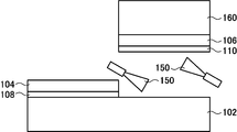
- 2 shows a cross section of the semiconductor device 100 in the manufacturing process.
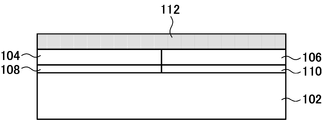
- 2 shows a cross section of the semiconductor device 100 in the manufacturing process.
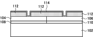
- 2 shows a cross section of the semiconductor device 100 in the manufacturing process.
- 2 shows a cross section of the semiconductor device 100 in the manufacturing process.
- 2 shows a cross section of the semiconductor device 100 in the manufacturing process.
- 2 shows a cross section of the semiconductor device 100 in the manufacturing process.
- FIG. 1 shows a cross section of a semiconductor device 100.
- 2 shows a cross section of the semiconductor device 100 in the manufacturing process.
- 2 shows a cross section of the semiconductor device 100 in the manufacturing process.
- 2 shows a cross section of the semiconductor device 100 in the manufacturing process.
- the cross section in the manufacture process of another semiconductor device is shown.
- the cross section in the manufacture process of another semiconductor device is shown.
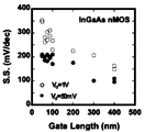
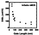
- a cross section of a semiconductor device 200 is shown. 2 shows a cross section of the semiconductor device 200 in the manufacturing process. It is the SEM photograph which observed nMOSFET from the upper part. It is the TEM photograph which observed the cross section of the gate part of nMOSFET. It is a graph which shows a gate voltage versus source current characteristic. It is a graph which shows a gate voltage versus source current characteristic. It is a graph which shows a gate voltage versus source current characteristic. It is the graph which showed SS value with respect to gate length. It is the graph which showed the value of DIBL with respect to gate length.
- FIG. 1 shows a cross section of the semiconductor device 100.
- the semiconductor device 100 includes a base substrate 102, a first semiconductor crystal layer 104, and a second semiconductor crystal layer 106.
- the semiconductor device 100 of this example includes a first separation layer 108 between the base substrate 102 and the first semiconductor crystal layer 104, and a second separation layer 110 between the base substrate 102 and the second semiconductor crystal layer 106.
- a first MISFET 120 is formed on the first semiconductor crystal layer 104
- a second MISFET 130 is formed on the second semiconductor crystal layer 106.
- Examples of the base substrate 102 include a substrate whose surface is a silicon crystal.
- Examples of the substrate whose surface is a silicon crystal include a silicon substrate and an SOI (Silicon-on-Insulator) substrate, and a silicon substrate is preferable.
- SOI Silicon-on-Insulator
- the base substrate 102 is not limited to a substrate whose surface is a silicon crystal, and may be an insulator substrate such as glass, ceramics, and plastic, a conductor substrate such as metal, or a semiconductor substrate such as silicon carbide.
- the first semiconductor crystal layer 104 is located above a part of the surface of the base substrate 102. That is, the first semiconductor crystal layer 104 is located above a partial region in the base substrate 102.
- the first semiconductor crystal layer 104 is made of a group IV semiconductor crystal or a group III-V compound semiconductor crystal.
- the thickness of the first semiconductor crystal layer 104 is preferably 20 nm or less. By setting the thickness of the first semiconductor crystal layer 104 to 20 nm or less, the first MISFET 120 having an extremely thin film body can be configured. By making the body of the first MISFET 120 an extremely thin film, the short channel effect can be suppressed and the leakage current of the first MISFET 120 can be reduced.
- the second semiconductor crystal layer 106 is located above another part different from the part of the surface of the base substrate 102. That is, the second semiconductor crystal layer 106 is located above the region of the base substrate 102 where the first semiconductor crystal layer 104 is not located above.
- the second semiconductor crystal layer 106 is made of a group III-V compound semiconductor crystal or a group IV semiconductor crystal.
- the thickness of the second semiconductor crystal layer 106 is preferably 20 nm or less. By setting the thickness of the second semiconductor crystal layer 106 to 20 nm or less, the second MISFET 130 having an extremely thin film body can be configured. By making the body of the second MISFET 130 an extremely thin film, the short channel effect can be suppressed and the leakage current of the second MISFET 130 can be reduced.
- the group III-V compound semiconductor crystal has a high electron mobility and the group IV semiconductor crystal, particularly Ge, has a high hole mobility, it is preferable to form an N-channel MISFET in the group III-V compound semiconductor crystal layer.
- a P-channel MISFET is preferably formed in the group IV semiconductor crystal layer. That is, when the first semiconductor crystal layer 104 is made of a group IV semiconductor crystal and the second semiconductor crystal layer 106 is made of a group III-V compound semiconductor crystal, the first MISFET 120 is a P-channel type MISFET and the second MISFET 130 is an N-channel type. A MISFET is preferable.
- the first MISFET 120 is an N-channel MISFET and the second MISFET 130 is a P-channel.
- a type MISFET is preferable.
- Examples of the group IV semiconductor crystal include a Ge crystal or a Si x Ge 1-x (0 ⁇ x ⁇ 1) crystal. When the group IV semiconductor crystal is a Si x Ge 1-x crystal, x is preferably 0.10 or less.
- Examples of the III-V compound semiconductor crystal include In x Ga 1-x As (0 ⁇ x ⁇ 1) crystal, InAs crystal, GaAs crystal, and InP crystal. Examples of the III-V compound semiconductor crystal include a mixed crystal of a III-V compound semiconductor that lattice matches or pseudo-lattice matches with GaAs or InP.
- examples of the III-V compound semiconductor crystal include a stacked body of the mixed crystal and In x Ga 1-x As (0 ⁇ x ⁇ 1) crystal, InAs crystal, GaAs crystal, or InP crystal.
- As the III-V compound semiconductor crystal an In x Ga 1-x As (0 ⁇ x ⁇ 1) crystal and an InAs crystal are preferable, and an InAs crystal is more preferable.
- the first separation layer 108 is located between the base substrate 102 and the first semiconductor crystal layer 104.
- the first separation layer 108 electrically separates the base substrate 102 and the first semiconductor crystal layer 104.
- the first separation layer 108 may be made of an amorphous insulator.
- the first separation layer 108 is made of an amorphous insulator.
- the first separation layer 108 may be made of a semiconductor crystal having a forbidden band width larger than the forbidden band width of the semiconductor crystal constituting the first semiconductor crystal layer 104.
- a semiconductor crystal can be formed by an epitaxial crystal growth method.
- the semiconductor crystal constituting the first separation layer 108 include an AlGaAs crystal, an AlInGaP crystal, an AlGaInAs crystal, and an InP crystal.
- the semiconductor crystal constituting the first separation layer 108 includes a SiGe crystal, a Si crystal, a SiC crystal, or a C crystal.
- the second separation layer 110 is located between the base substrate 102 and the second semiconductor crystal layer 106.
- the second separation layer 110 electrically separates the base substrate 102 and the second semiconductor crystal layer 106.
- the second separation layer 110 may be made of an amorphous insulator.
- the second separation layer 110 becomes an amorphous insulator.
- the second separation layer 110 made of an amorphous insulator Al 2 O 3 , AlN, Ta 2 O 5 , ZrO 2 , HfO 2 , La 2 O 3 , SiO x (for example, SiO 2 ), SiN x (for example, Si) 3 N 4 ) and SiO x N y , or a laminate of at least two layers selected from these layers.
- the second isolation layer 110 may be made of a semiconductor crystal having a forbidden band width larger than the forbidden band width of the semiconductor crystal constituting the second semiconductor crystal layer 106. Such a semiconductor crystal can be formed by an epitaxial crystal growth method.
- the semiconductor crystal layer 106 is an InGaAs crystal layer or a GaAs crystal layer
- examples of the semiconductor crystal constituting the second separation layer 110 include an AlGaAs crystal, an AlInGaP crystal, an AlGaInAs crystal, and an InP crystal.
- examples of the semiconductor crystal constituting the second separation layer 110 include SiGe crystal, Si crystal, SiC crystal, and C crystal.
- the first MISFET 120 is formed in the first semiconductor crystal layer 104 and has a first gate 122, a first source 124 and a first drain 126.
- a first gate metal 123 is formed on the first gate 122, and a first source electrode 125 and a first drain electrode 127 are formed on the first source 124 and the first drain 126, respectively.
- Examples of the material constituting the first gate metal 123, the first source electrode 125, and the first drain electrode 127 include Ti, Ta, W, Al, Cu, Au, and a stacked body thereof.
- the first source 124 and the first drain 126 are made of a conductive material formed on the first semiconductor crystal layer 104, and form a raised source / drain.
- the conductive material include TiN, TaN, graphene, HfN, and WN.
- a first gate 122 is formed between the first source 124 and the first drain 126.
- the first gate 122 is insulated from the first source 124, the first drain 126, and the first semiconductor crystal layer 104 by the insulating layer 114.
- Examples of the material constituting the first gate 122 include TiN, TaN, graphene, HfN, and WN.
- the insulating layer 114 Al 2 O 3 , AlN, Ta 2 O 5 , ZrO 2 , HfO 2 , La 2 O 3 , SiO x (for example, SiO 2 ), SiN x (for example, Si 3 N 4 ), and SiO x N y Among them, a layer composed of at least one of them, or a laminate of at least two layers selected from these.
- a part 114 a of the insulating layer 114 is formed in a region sandwiched between the part 104 a of the first semiconductor crystal layer 104 and the first gate 122, which is the channel region.
- the portion 114a may function as a gate insulating layer.
- the second MISFET 130 is formed in the second semiconductor crystal layer 106 and has a second gate 132, a second source 134, and a second drain 136.
- a second gate metal 133 is formed on the second gate 132, and a second source electrode 135 and a second drain electrode 137 are formed on the second source 134 and the second drain 136, respectively.
- Examples of the material constituting the second gate metal 133, the second source electrode 135, and the second drain electrode 137 include Ti, Ta, W, Al, Cu, Au, or a laminate thereof.
- the second source 134 and the second drain 136 are made of a conductive material formed on the second semiconductor crystal layer 106, and constitute a raised source / drain.
- the conductive material include TiN, TaN, graphene, HfN, and WN.
- a second gate 132 is formed between the second source 134 and the second drain 136.
- the second gate 132 is insulated from the second source 134, the second drain 136, and the second semiconductor crystal layer 106 by the insulating layer 114 similar to the first MISFET 120.
- Examples of the material constituting the second gate 132 include TiN, TaN, graphene, HfN, and WN.
- a part 114 a of the insulating layer 114 is formed in a region sandwiched between the part 106 a of the second semiconductor crystal layer 106 and the second gate 132 which is the channel region.
- the portion 114a may function as a gate insulating layer.
- the first source 124, the first drain 126, the second source 134, and the second drain 136 are made of the same conductive material, and the work function ⁇ M of the conductive material satisfies the relationship of Equation 1 or Equation 2.
- Equation 1 ⁇ 1 ⁇ M ⁇ 2 + E g2
- phi 1 shows the electron affinity of the crystalline part of which constitutes a semiconductor crystal layer of better functioning as an N-type channel.
- ⁇ 2 and E g2 indicate the electron affinity and the forbidden band width of the crystal that constitutes the semiconductor crystal layer of which part of the first semiconductor crystal layer 104 and the second semiconductor crystal layer 106 functions as a P-type channel.
- the work function ⁇ M of the conductive material may satisfy both of the relations of Formula 1 and Formula 2.
- the source / drain (first source 124 and first drain 126) of the first MISFET 120 and the source / drain (second source 134 and second drain 136) of the second MISFET 130 are made of the same conductive material. This is a configuration that enables the manufacture of the part using the same material film, and means that the manufacturing process can be simplified.
- the gate width can be easily controlled by the space between the source and the drain (etching groove interval). As a result, miniaturization becomes easy.
- the source / drain The contact resistance between the region and the semiconductor crystal layer can be reduced.
- the work function ⁇ M of the conductive material satisfies the relationship of Equation 1
- the difference between ⁇ M and ⁇ 1 and the difference between ⁇ M and ⁇ 2 + E g2 are ⁇ 1 and ⁇ 2 at the maximum. It becomes smaller than the difference from + Eg2 .
- the contact resistance between each source / drain region and the semiconductor crystal layer can be reduced.
- the work function ⁇ M of the conductive material satisfies the relationship of Equation 2 , the difference between ⁇ M and ⁇ 1 and the difference between ⁇ M and ⁇ 2 + E g2 can be suppressed to 0.1 eV or less. . For this reason, the contact resistance between each source / drain region and the semiconductor crystal layer can be reduced. As a result, the manufacturing process for manufacturing the CMISFET can be simplified, the miniaturization can be facilitated, and the performance of each FET can be enhanced.
- FIG. 2 to 8 show cross sections in the manufacturing process of the semiconductor device 100.
- the base substrate 102 and the semiconductor crystal layer formation substrate 140 are prepared, and the first semiconductor crystal layer 104 is formed on the semiconductor crystal layer formation substrate 140 by an epitaxial crystal growth method. Thereafter, a first separation layer 108 is formed on the first semiconductor crystal layer 104.
- the first separation layer 108 is formed by a thin film formation method such as an ALD (Atomic Layer Deposition) method, a thermal oxidation method, a vapor deposition method, a CVD (Chemical Layer Vapor Deposition) method, or a sputtering method.
- the semiconductor crystal layer formation substrate 140 When the first semiconductor crystal layer 104 is made of a III-V group compound semiconductor crystal, an InP substrate or a GaAs substrate can be selected as the semiconductor crystal layer formation substrate 140. When the first semiconductor crystal layer 104 is made of a group IV semiconductor crystal, a Ge substrate, Si substrate, SiC substrate, or GaAs substrate can be selected as the semiconductor crystal layer formation substrate 140.
- An MOCVD (Metal Organic Chemical Vapor Deposition) method can be used for epitaxial crystal growth of the first semiconductor crystal layer 104.
- TMIn trimethylindium
- TMGa trimethylgallium
- AsH 3 arsine
- P source is used.
- PH 3 phosphine
- Hydrogen can be used as the carrier gas.
- the reaction temperature can be appropriately selected in the range of 300 ° C. to 900 ° C., preferably in the range of 450 to 750 ° C.
- GeH 4 germane
- SiH 4 silane
- Si 2 H 6 diisilane
- a compound in which a part of the plurality of hydrogen atom groups is substituted with a chlorine atom or a hydrocarbon group can also be used.
- Hydrogen can be used as the carrier gas.
- the reaction temperature can be appropriately selected in the range of 300 ° C. to 900 ° C., preferably in the range of 450 to 750 ° C.
- the thickness of the epitaxial growth layer can be controlled by appropriately selecting the source gas supply amount and the reaction time.
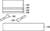
- the surface of the first separation layer 108 and the surface of the base substrate 102 are activated with an argon beam 150. Thereafter, as shown in FIG. 3, the surface of the first separation layer 108 activated by the argon beam 150 is bonded and bonded to a part of the surface of the base substrate 102. Bonding can be performed at room temperature. The activation does not need to be performed by the argon beam 150, but may be a beam of other rare gas or the like. Thereafter, the semiconductor crystal layer forming substrate 140 is etched and removed. As a result, the first separation layer 108 and the first semiconductor crystal layer 104 are formed on part of the surface of the base substrate 102. Note that a sulfur termination treatment for terminating the surface of the first semiconductor crystal layer 104 with sulfur atoms may be performed between the formation of the first semiconductor crystal layer 104 and the formation of the first separation layer 108.
- the first separation layer 108 is formed only on the first semiconductor crystal layer 104 and the surface of the first separation layer 108 and the surface of the base substrate 102 are bonded to each other.
- the first separation layer 108 is also formed on the base substrate 102, and the surface of the first separation layer 108 on the first semiconductor crystal layer 104 and the surface of the first separation layer 108 on the base substrate 102 are bonded together. May be.
- the surface of the first separation layer 108 to be bonded is subjected to a hydrophilic treatment. When the hydrophilic treatment is performed, it is preferable that the first separation layers 108 are heated and bonded together.
- the first separation layer 108 may be formed only on the base substrate 102, and the surface of the first semiconductor crystal layer 104 and the surface of the first separation layer 108 on the base substrate 102 may be bonded to each other.
- the first separation layer 108 and the first semiconductor crystal layer 104 are bonded to the semiconductor crystal layer formation substrate.
- the first separation layer 108 and the first semiconductor crystal layer 104 are separated from the base substrate 102. You may stick together.
- the first separation layer 108 and the first semiconductor crystal layer 104 are separated from the semiconductor crystal layer formation substrate 140 and before being bonded to the base substrate 102, the first separation layer 108 and the first separation layer 108 are formed on an appropriate transfer substrate. It is preferable to hold one semiconductor crystal layer 104.
- a semiconductor crystal layer forming substrate 160 is prepared, and the second semiconductor crystal layer 106 is formed on the semiconductor crystal layer forming substrate 160 by an epitaxial crystal growth method. Thereafter, the second separation layer 110 is formed on the second semiconductor crystal layer 106.
- the second separation layer 110 is formed by a thin film forming method such as an ALD method, a thermal oxidation method, a vapor deposition method, a CVD method, or a sputtering method. Note that a sulfur termination treatment for terminating the surface of the second semiconductor crystal layer 106 with sulfur atoms may be performed before the formation of the second separation layer 110.
- the semiconductor crystal layer 106 is made of a III-V group compound semiconductor crystal
- an InP substrate or a GaAs substrate can be selected as the semiconductor crystal layer forming substrate 160.
- the second semiconductor crystal layer 106 is made of a group IV semiconductor crystal
- a Ge substrate, Si substrate, SiC substrate, or GaAs substrate can be selected as the semiconductor crystal layer forming substrate 160.
- the MOCVD method can be used for epitaxial crystal growth of the second semiconductor crystal layer 106.
- Gas used in the MOCVD method, reaction temperature conditions, and the like are the same as those for the first semiconductor crystal layer 104.
- the surface of the base substrate 102 and the surface of the second separation layer 110 in the region where the first separation layer 108 and the first semiconductor crystal layer 104 are not formed are activated with an argon beam 150.
- the surface of the second separation layer 110 is bonded and bonded to the surface of the base substrate 102 in a region where the first separation layer 108 and the first semiconductor crystal layer 104 are not formed. Bonding can be performed at room temperature. The activation does not need to be performed by the argon beam 150 but may be a beam of other rare gas or the like.
- the semiconductor crystal layer forming substrate 160 is removed by etching with an HCl solution or the like.
- the second separation layer 110 and the second semiconductor crystal layer 106 are formed on the base substrate 102 in a region where the first separation layer 108 and the first semiconductor crystal layer 104 are not formed.
- the semiconductor crystal layer forming substrate 140 and the semiconductor crystal layer forming substrate 160 may be removed at the same time. That is, after the second separation layer 110 in both the semiconductor crystal layer formation substrate 140 and the semiconductor crystal layer formation substrate 160 is bonded to the base substrate 102, the semiconductor crystal layer formation substrate 140 and the semiconductor crystal layer formation substrate 160 are removed. Good.
- the second separation layer 110 is formed only on the second semiconductor crystal layer 106 and the surface of the second separation layer 110 and the surface of the base substrate 102 are bonded to each other.
- the second separation layer 110 may also be formed over the substrate 102, and the surface of the second separation layer 110 over the second semiconductor crystal layer 106 and the surface of the second separation layer 110 over the base substrate 102 may be bonded together. .
- the second separation layer 110 may be formed only on the base substrate 102 and the surface of the base substrate 102 and the surface of the second separation layer 110 on the second semiconductor crystal layer 106 may be bonded to each other.
- the second semiconductor crystal layer 106 and the second separation layer 110 are bonded to the base substrate 102 and then the second semiconductor crystal layer 106 is separated from the semiconductor crystal layer formation substrate 160 has been described.
- the second semiconductor crystal layer 106 may be bonded to the base substrate 102.
- the second semiconductor crystal layer 106 and the second separation layer 110 are separated from the semiconductor crystal layer formation substrate 160 and before being bonded to the base substrate 102, the second semiconductor crystal layer 106 and the second semiconductor crystal layer 106 and It is preferable to hold the second separation layer 110.
- a conductive material layer 112 is formed on the first semiconductor crystal layer 104 and the second semiconductor crystal layer 106.
- the conductive material layer 112 becomes the first source 124, the first drain 126, the second source 134, and the second drain 136 later.
- the conductive material layer 112 is formed by a thin film formation method such as a vapor deposition method, a CVD method, or a sputtering method.
- the conductive material layer 112 in the region where the first gate 122 and the second gate 132 are formed is removed by etching to form an insulating layer 114.
- the insulating layer 114 is formed by a thin film forming method such as an ALD method, a thermal oxidation method, a vapor deposition method, a CVD method, or a sputtering method.
- a conductive thin film is formed on the insulating layer 114, and the conductive thin films other than the regions to be the first gate 122 and the second gate 132 are removed, so that the first gate 122 and the second gate A gate 132 is formed.
- the conductive material layer 112 separated by the first gate 122 or the second gate 132 becomes the first source 124, the first drain 126, the second source 134, and the second drain 136.
- An opening is formed in the insulating layer 114 so that the conductive material layer 112 to be the first source 124, the first drain 126, the second source 134, and the second drain 136 is exposed, and the first thin film is formed and patterned to form the first.
- the semiconductor device 100 shown in FIG. 1 can be manufactured.
- a metal film is formed as the conductive thin film, it is preferable to perform post metal annealing treatment.
- the post metal annealing treatment is preferably carried out by an RTA (rapid thermal annealing) method.
- the first source 124, the first drain 126, the second source 134, and the second drain 136 are simultaneously formed in the same process, so that the manufacturing process can be simplified. .
- manufacturing costs are reduced and miniaturization is facilitated.
- the work functions of the conductive materials constituting the first source 124, the first drain 126, the second source 134, and the second drain 136 satisfy the relationship represented by Equation 1 or Equation 2. Therefore, the contact between the first source 124 and the first drain 126 and the first semiconductor crystal layer 104 is an ohmic contact, and the contact between the second source 134 and the second drain 136 and the second semiconductor crystal layer 106 is an ohmic contact.
- each on-current of the first MISFET 120 and the second MISFET 130 can be increased. Further, since the resistance between each source and drain is reduced, it is not necessary to reduce the channel resistance of each MISFET, and the concentration of doping impurity atoms in the channel layer can be reduced. As a result, carrier mobility in the channel layer can be increased.
- the first separation of the base substrate 102 is performed.
- a voltage can be applied to a region in contact with the layer 108 and the voltage can act as a back gate voltage to the first MISFET 120.
- the base substrate 102 and the second separation layer 110 are in contact with each other, if the region of the base substrate 102 in contact with the second separation layer 110 is conductive, A voltage can be applied to a region in contact with the two isolation layers 110, and the voltage can act as a back gate voltage to the second MISFET 130. The action of these back gate voltages can increase the on-current of the first MISFET 120 and the second MISFET 130 and reduce the off-current.
- the semiconductor device 100 described above may include a plurality of first semiconductor crystal layers 104, and each of the plurality of first semiconductor crystal layers 104 may be regularly arranged in a plane parallel to the upper surface of the base substrate 102. Regular means that the same arrangement pattern is repeated, for example.
- the semiconductor device 100 may include a plurality of second semiconductor crystal layers 106, and each of the plurality of second semiconductor crystal layers 106 may be regularly arranged in a plane parallel to the upper surface of the base substrate 102.
- the semiconductor device 100 may regularly include a plurality of both the first semiconductor crystal layer 104 and the second semiconductor crystal layer 106. Thus, by regularly arranging the first semiconductor crystal layer 104 and the second semiconductor crystal layer 106, the productivity of the semiconductor substrate used for the semiconductor device 100 can be increased.
- the regular arrangement of the second semiconductor crystal layer 106 or the first semiconductor crystal layer 104 is such that the second semiconductor crystal layer 106 or the first semiconductor crystal layer is grown after the second semiconductor crystal layer 106 or the first semiconductor crystal layer 104 is epitaxially grown.
- the first semiconductor crystal layer 104 and the first isolation layer 108 are formed on the semiconductor crystal layer formation substrate 140, and the first isolation layer 108 and the base substrate 102 are bonded together, and then the semiconductor crystal layer formation is performed.
- the semiconductor crystal layer formation substrate 160 By removing the substrate 140, the first semiconductor crystal layer 104 and the first separation layer 108 are formed on the base substrate 102, and the second semiconductor crystal layer 106 and the second separation layer 110 are formed on the semiconductor crystal layer formation substrate 160.
- the second semiconductor crystal layer 106 and the second separation layer 110 are formed on the base substrate 102 by removing the semiconductor crystal layer formation substrate 160 after forming and bonding the second separation layer 110 and the base substrate 102 together. I explained that.
- the semiconductor crystal layer and the separation layer made of SiGe are It can also be formed by an oxidation concentration method.
- the first semiconductor crystal layer 104 is made of SiGe. That is, before forming the first semiconductor crystal layer 104, the first separation layer 108 made of an insulator is formed on the base substrate 102, and the first semiconductor crystal layer 104 starts on the first separation layer 108. A SiGe layer as a material is formed. The SiGe layer is heated in an oxidizing atmosphere to oxidize the surface.
- the concentration of Ge atoms in the SiGe layer can be increased, and the first semiconductor crystal layer 104 having a high Ge concentration can be obtained. Thereafter, the SiGe layer in the region where the second semiconductor crystal layer 106 is formed is removed by etching to form the first semiconductor crystal layer 104.
- the semiconductor crystal made of the group IV semiconductor crystal can be formed by a smart cut method.
- the first semiconductor crystal layer 104 is made of a group IV semiconductor crystal. That is, a first separation layer 108 made of an insulator is formed on the surface of a semiconductor layer material substrate made of a group IV semiconductor crystal, and cations are implanted through the first separation layer 108 to a predetermined separation depth of the semiconductor layer material substrate. To do.
- the semiconductor layer material substrate and the base substrate 102 are attached to each other so that the surface of the first separation layer 108 and the surface of the base substrate 102 are bonded, and the semiconductor layer material substrate and the base substrate 102 are heated. By this heating, the cations implanted at the planned separation depth react with the group IV atoms constituting the semiconductor layer material substrate, and the group IV semiconductor crystal located at the planned separation depth is denatured. If the semiconductor layer material substrate and the base substrate 102 are separated in this state, the group IV semiconductor crystal located on the base substrate 102 side from the modified group of the group IV semiconductor crystal is separated from the semiconductor layer material substrate.
- One semiconductor crystal layer 104 can be formed.
- any one of the first separation layer 108 and the second separation layer 110 is a semiconductor crystal having a forbidden band width larger than the forbidden band width of the semiconductor crystal layer located thereon, the separation is performed.
- the layer can be formed continuously up to the semiconductor crystal layer using an epitaxial growth method.
- the first separation layer 108 is made of a semiconductor crystal will be described.
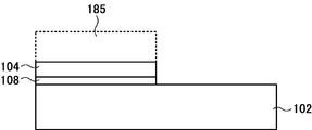
- a first separation layer 108 is formed on the base substrate 102 by an epitaxial growth method, and a first semiconductor crystal layer 104 is formed on the first separation layer 108 by an epitaxial growth method. After the epitaxial growth, as shown in FIG.
- the first semiconductor crystal layer 104 and the first separation layer 108 in the region where the second semiconductor crystal layer 106 is formed are removed by etching.
- a semiconductor substrate similar to that shown in FIG. 3 can be obtained.
- the first separation layer 108 and the first semiconductor crystal layer 104 can be formed continuously, or the second separation layer 110 and the second semiconductor crystal layer 106 can be formed continuously by the epitaxial growth method, so that the manufacturing process is simple. become.
- the first layer is formed using the selective epitaxial growth method.
- the separation layer 108 and the first semiconductor crystal layer 104 or the second separation layer 110 and the second semiconductor crystal layer 106 can be formed.
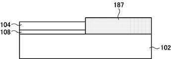
- the region where the second isolation layer 110 and the second semiconductor crystal layer 106 are formed on the surface of the base substrate 102 is covered with a growth inhibition layer 187 such as SiO 2 and epitaxial growth is performed.
- the first semiconductor crystal layer 104 and the first separation layer 108 are selectively epitaxially grown on the base substrate 102 in a region where the growth inhibition layer 187 does not exist. Thereafter, the growth inhibition layer 187 is removed, and a semiconductor substrate similar to that shown in FIG. 3 can be obtained.
- the first separation layer 108 or the second separation layer 110 may be oxidized to be converted into an amorphous insulator layer.
- the first separation layer 108 or the second separation layer 110 is AlAs or AlInP
- the first separation layer 108 or the second separation layer 110 can be made into an insulating oxide by a selective oxidation technique.
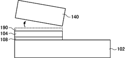
- the substrate can also be removed. That is, before forming the first semiconductor crystal layer 104 on the semiconductor crystal layer formation substrate 140, the crystalline sacrificial layer 190 is formed on the surface of the semiconductor crystal layer formation substrate 140 by an epitaxial crystal growth method. Thereafter, the first semiconductor crystal layer 104 and the first separation layer 108 are formed on the surface of the crystalline sacrificial layer 190 by an epitaxial growth method, and the surface of the first separation layer 108 and the surface of the base substrate 102 are activated by the argon beam 150. .
- the semiconductor crystal layer forming substrate can be reused, and the manufacturing cost can be reduced.
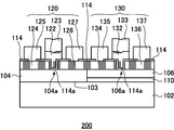
- FIG. 13 shows a cross section of the semiconductor device 200.
- the semiconductor device 200 does not have the first separation layer 108 in the semiconductor device 100, and the first semiconductor crystal layer 104 is disposed in contact with the base substrate 102.
- the first separation layer 108 since it has the same structure as the semiconductor device 100 except that the first separation layer 108 is not provided, description of common members and the like is omitted.
- the base substrate 102 and the first semiconductor crystal layer 104 are in contact with each other at the bonding surface 103, and contain impurity atoms having p-type or n-type conductivity in the vicinity of the bonding surface 103 of the base substrate 102.
- impurity atoms having a conductivity type different from the conductivity type indicated by the impurity atoms contained in the base substrate 102 are contained. That is, the semiconductor device 200 has a pn junction in the vicinity of the bonding surface 103.
- the base substrate 102 and the first semiconductor crystal layer 104 can be electrically separated by a pn junction formed in the vicinity of the bonding surface 103.
- the first MISFET 120 formed in the semiconductor crystal layer 104 can be electrically isolated from the base substrate 102.
- the semiconductor device 200 can be manufactured as follows. As shown in FIG. 14, a first semiconductor crystal layer 104 is formed on the entire surface of the base substrate 102 by an epitaxial growth method. Then, the first semiconductor crystal layer 104 in the region where the second semiconductor crystal layer 106 is formed is removed by etching. The second isolation layer 110 and the second semiconductor crystal layer 106 are formed on the base substrate 102 in the region where the first semiconductor crystal layer 104 has been removed, by the same process as that described with reference to FIGS. Subsequent steps are the same as those of the semiconductor device 100.
- the base substrate 102 is formed in a step in which impurity atoms having p-type or n-type conductivity are contained in the vicinity of the surface of the base substrate 102 and the first semiconductor crystal layer 104 is formed by the epitaxial growth method.
- the first semiconductor crystal layer 104 can be doped with an impurity atom having a conductivity type different from that of the impurity atom contained in the first semiconductor crystal layer 104.
- the pn junction as the isolation structure is not essential when the need for element isolation is low. That is, the semiconductor device 200 does not contain an impurity atom having p-type or n-type conductivity in the vicinity of the bonding surface 103 of the base substrate 102, and is p-type or in the vicinity of the bonding surface 103 of the first semiconductor crystal layer 104. A structure not containing an impurity atom exhibiting n-type conductivity may be used.
- the epitaxial growth method is a method in which the first semiconductor crystal layer 104 is uniformly grown on the entire surface of the base substrate 102, or the surface of the base substrate 102 is divided finely by a growth inhibition layer such as SiO 2 and selectively. Any epitaxial growth method may be used.
- a Ge crystal layer was formed on a part of the surface of the base substrate, and an InGaAs crystal layer was formed on the other part of the surface of the base substrate, that is, on the base substrate in a region where the Ge crystal layer was not formed.
- a TaN layer having a thickness of 30 nm was deposited on the InGaAs crystal layer and the Ge crystal layer, and the TaN layer was patterned. By the patterning, a source and a drain were formed on each of the InGaAs crystal layer and the Ge crystal layer.
- An Al 2 O 3 / TaN laminated film was deposited in the order of Al 2 O 3 and TaN so as to fill the trench between the source and the drain, and the deposited layer was patterned to form a gate insulating film and a gate.
- Four types of devices having a source-drain groove width that is, a gate length of 50 nm, 75 nm, 100 nm, and 100 ⁇ m were formed.
- the nMOSFET was formed on the InGaAs crystal layer
- the pMOSFET was formed on the Ge crystal layer
- the source and drain were simultaneously formed.
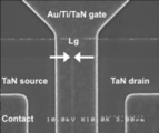
- FIG. 15 is a SEM photograph of the nMOSFET observed from above.
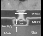
- FIG. 16 is a TEM photograph observing a cross section of the gate portion of the nMOSFET. Even when the gate length Lg is 50 nm, it can be confirmed that the trench between the source and the drain is securely buried.
- the source / drain made of TaN formed as described above has a work function of about 4.6 eV.
- the electron affinity of InGaAs is 4.5 eV
- the electron affinity of Ge is 4.0 eV
- the band gap of Ge is 0.67 eV. Therefore, the work function ⁇ M of the source / drain is such that the electron affinity ⁇ 1 of InGaAs which is an nMOSFET material and the sum of electron affinity and band gap ⁇ 2 + E g2 of Ge which is a pMOSFET material are ⁇ 1 ⁇ M ⁇ The relationship of 2 + E g2 is satisfied.
- between the work function ⁇ M of the source / drain and the electron affinity ⁇ 1 of InGaAs is 0.1 eV or less, and the work function ⁇ M of the source / drain and the electron affinity of Ge and The sum of the band gap ⁇ 2 + E g2 and the difference
- are also 0.1 eV or less.
- the barrier between TaN and InGaAs when conducting n-type conduction is small, and the barrier between TaN and Ge when conducting p-type conduction is also small. That is, the contact resistance of the source / drain can be reduced by adopting TaN using the source / drain of the nMOSFET on the InGaAs crystal layer and the pMOSFET on the Ge crystal layer as a common electrode material.
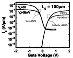
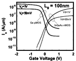
- FIG. 17 and 18 are graphs showing gate voltage versus source current characteristics in the pMOSFET and nMOSFET included in the device of Example 1.
- FIG. 17 shows a case where the gate length Lg is 100 ⁇ m, and FIG. The case of 100 nm is shown.
- Each figure shows two types of data when the drain voltage Vd is 1V and when it is 50 mV.
- Lg was 100 ⁇ m
- a 4-digit on / off ratio was observed in the pMOSFET on the Ge crystal layer
- a 6-digit on / off ratio was observed in the nMOSFE on the InGaAs crystal layer.
- FIG. 19 is a graph showing the gate voltage vs. source current characteristics, and shows the data for the nMOSFE on the InGaAs crystal layer when the gate length Lg is made smaller than that shown in FIG. Although the off-current increases due to the short channel effect and the subthreshold characteristic (SS value) deteriorates, switching characteristics were observed even when the gate length was 50 nm.
- SS value subthreshold characteristic
- FIG. 20 is a graph showing the SS value with respect to the gate length
- FIG. 21 is a graph showing a DIBL (drain-induced barrier lowering) value with respect to the gate length.
- 100 semiconductor device 102 base substrate, 103 bonding surface, 104 first semiconductor crystal layer, 104a part of first semiconductor crystal layer, 106 second semiconductor crystal layer, 106a part of second semiconductor crystal layer, 108 first separation 110, second isolation layer, 112 conductive material layer, 114 insulating layer, 114a, part of insulating layer, 120 first MISFET, 122 first gate, 123 first gate metal, 124 first source, 125 first source electrode , 126 1st drain, 127 1st drain electrode, 130 2nd MISFET, 132 2nd gate, 133 2nd gate metal, 134 2nd source, 135 2nd source electrode, 136 2nd drain, 137 2nd drain electrode, 140 Semiconductor crystal layer forming substrate, 150 argon beam, 1 0 semiconductor crystal layer forming the substrate, 185 a mask, 187 growth inhibition layer, 190 crystalline sacrificial layer, 200 a semiconductor device
Landscapes
- Metal-Oxide And Bipolar Metal-Oxide Semiconductor Integrated Circuits (AREA)
- Thin Film Transistor (AREA)
- Electrodes Of Semiconductors (AREA)
Abstract
Une première source et un premier drain pour un premier MISFET de premier type de canal formé sur une première couche de cristal semi-conducteur et une seconde source et un second drain pour un second MISFET d'un second type de canal formé sur une seconde couche de cristal semi-conducteur comprennent le même matériau conducteur et le travail d'extraction (ΦM) pour ledit matériau conducteur respecte au moins la formule 1 ou la formule 2. (Formule 1) φ1<ΦM<φ2+Eg2 (Formule 2) |ΦM-φ1|≦0,1 eV et |(φ2+Eg2)-ΦM|≦0,1 eV. φ1
est l'affinité électronique pour une couche de cristal semi-conducteur de type n, et φ2
et Eg2
sont l'affinité électronique et la largeur de bande interdite pour une couche de cristal semi-conducteur de type p.
Applications Claiming Priority (2)
| Application Number | Priority Date | Filing Date | Title |
|---|---|---|---|
| JP2011130730 | 2011-06-10 | ||
| JP2011-130730 | 2011-06-10 |
Publications (1)
| Publication Number | Publication Date |
|---|---|
| WO2012169214A1 true WO2012169214A1 (fr) | 2012-12-13 |
Family
ID=47295797
Family Applications (1)
| Application Number | Title | Priority Date | Filing Date |
|---|---|---|---|
| PCT/JP2012/003789 Ceased WO2012169214A1 (fr) | 2011-06-10 | 2012-06-11 | Dispositif semi-conducteur, substrat semi-conducteur, procédé de production de substrat semi-conducteur, et procédé de production de dispositif semi-conducteur |
Country Status (3)
| Country | Link |
|---|---|
| JP (1) | JP2013016792A (fr) |
| TW (1) | TW201306236A (fr) |
| WO (1) | WO2012169214A1 (fr) |
Families Citing this family (2)
| Publication number | Priority date | Publication date | Assignee | Title |
|---|---|---|---|---|
| JP2014187238A (ja) * | 2013-03-25 | 2014-10-02 | Toyoda Gosei Co Ltd | Mis型半導体装置の製造方法 |
| KR102104062B1 (ko) * | 2013-10-31 | 2020-04-23 | 삼성전자 주식회사 | 기판 구조체, 이를 포함한 cmos 소자 및 cmos 소자 제조 방법 |
Citations (8)
| Publication number | Priority date | Publication date | Assignee | Title |
|---|---|---|---|---|
| JPS59198750A (ja) * | 1983-04-25 | 1984-11-10 | Seiko Epson Corp | 半導体装置 |
| JPS63311768A (ja) * | 1987-06-13 | 1988-12-20 | Fujitsu Ltd | 相補型半導体装置の製造方法 |
| JPH0384960A (ja) * | 1989-08-28 | 1991-04-10 | Nec Corp | 半導体装置 |
| JPH03109740A (ja) * | 1989-09-25 | 1991-05-09 | Hitachi Ltd | 半導体装置 |
| JPH0969611A (ja) * | 1995-09-01 | 1997-03-11 | Hitachi Ltd | 半導体装置およびその製造方法 |
| JP2001093987A (ja) * | 1999-07-29 | 2001-04-06 | Stmicroelectronics Inc | Si基板上のGaAs/Geの新規なCMOS回路 |
| JP2007013025A (ja) * | 2005-07-04 | 2007-01-18 | Matsushita Electric Ind Co Ltd | 電界効果型トランジスタおよびその製造方法 |
| JP2009503871A (ja) * | 2005-07-26 | 2009-01-29 | アンバーウェーブ システムズ コーポレイション | 代替活性エリア材料の集積回路への組み込みのための解決策 |
-
2012
- 2012-06-08 TW TW101120841A patent/TW201306236A/zh unknown
- 2012-06-11 WO PCT/JP2012/003789 patent/WO2012169214A1/fr not_active Ceased
- 2012-06-11 JP JP2012131891A patent/JP2013016792A/ja active Pending
Patent Citations (8)
| Publication number | Priority date | Publication date | Assignee | Title |
|---|---|---|---|---|
| JPS59198750A (ja) * | 1983-04-25 | 1984-11-10 | Seiko Epson Corp | 半導体装置 |
| JPS63311768A (ja) * | 1987-06-13 | 1988-12-20 | Fujitsu Ltd | 相補型半導体装置の製造方法 |
| JPH0384960A (ja) * | 1989-08-28 | 1991-04-10 | Nec Corp | 半導体装置 |
| JPH03109740A (ja) * | 1989-09-25 | 1991-05-09 | Hitachi Ltd | 半導体装置 |
| JPH0969611A (ja) * | 1995-09-01 | 1997-03-11 | Hitachi Ltd | 半導体装置およびその製造方法 |
| JP2001093987A (ja) * | 1999-07-29 | 2001-04-06 | Stmicroelectronics Inc | Si基板上のGaAs/Geの新規なCMOS回路 |
| JP2007013025A (ja) * | 2005-07-04 | 2007-01-18 | Matsushita Electric Ind Co Ltd | 電界効果型トランジスタおよびその製造方法 |
| JP2009503871A (ja) * | 2005-07-26 | 2009-01-29 | アンバーウェーブ システムズ コーポレイション | 代替活性エリア材料の集積回路への組み込みのための解決策 |
Also Published As
| Publication number | Publication date |
|---|---|
| JP2013016792A (ja) | 2013-01-24 |
| TW201306236A (zh) | 2013-02-01 |
Similar Documents
| Publication | Publication Date | Title |
|---|---|---|
| CN103548133B (zh) | 半导体器件、半导体基板、半导体基板的制造方法及半导体器件的制造方法 | |
| CN105762080B (zh) | 具有替代通道材料的电性绝缘鳍片结构及其制法 | |
| US20140091398A1 (en) | Semiconductor device, semiconductor wafer, method for producing semiconductor wafer, and method for producing semiconductor device | |
| US8653599B1 (en) | Strained SiGe nanowire having (111)-oriented sidewalls | |
| JP5678485B2 (ja) | 半導体装置 | |
| TWI690975B (zh) | 應力堆疊奈米片鰭狀電晶體及/或量子井堆疊奈米片 | |
| JP6560117B2 (ja) | 半導体装置の製造方法 | |
| CN103563068B (zh) | 半导体器件、半导体基板、半导体基板的制造方法及半导体器件的制造方法 | |
| WO2012169214A1 (fr) | Dispositif semi-conducteur, substrat semi-conducteur, procédé de production de substrat semi-conducteur, et procédé de production de dispositif semi-conducteur | |
| US9818761B2 (en) | Selective oxidation for making relaxed silicon germanium on insulator structures | |
| JP2004055943A (ja) | 半導体装置とその製造方法 | |
| WO2012169210A1 (fr) | Dispositif à semi-conducteurs, substrat semi-conducteur, et procédé de fabrication de ceux-ci | |
| JP6083707B2 (ja) | 半導体装置およびその製造方法 | |
| JP7444285B2 (ja) | 半導体構造および電界効果トランジスタの作製方法 | |
| CN106611793A (zh) | 应变堆叠的纳米片fet和/或量子阱堆叠的纳米片 | |
| Hartmann | Si, SiGe, and Si (1− y) Cy on Si: Epitaxy of Group-IV Semiconductors for Nanoelectronics |
Legal Events
| Date | Code | Title | Description |
|---|---|---|---|
| 121 | Ep: the epo has been informed by wipo that ep was designated in this application |
Ref document number: 12796189 Country of ref document: EP Kind code of ref document: A1 |
|
| NENP | Non-entry into the national phase |
Ref country code: DE |
|
| 122 | Ep: pct application non-entry in european phase |
Ref document number: 12796189 Country of ref document: EP Kind code of ref document: A1 |