WO2012169408A1 - 回路基板およびこれを備える電子装置 - Google Patents
回路基板およびこれを備える電子装置 Download PDFInfo
- Publication number
- WO2012169408A1 WO2012169408A1 PCT/JP2012/063946 JP2012063946W WO2012169408A1 WO 2012169408 A1 WO2012169408 A1 WO 2012169408A1 JP 2012063946 W JP2012063946 W JP 2012063946W WO 2012169408 A1 WO2012169408 A1 WO 2012169408A1
- Authority
- WO
- WIPO (PCT)
- Prior art keywords
- region
- conductor
- hole
- circuit board
- crystal grain
- Prior art date
- Legal status (The legal status is an assumption and is not a legal conclusion. Google has not performed a legal analysis and makes no representation as to the accuracy of the status listed.)
- Ceased
Links
Images


Classifications
-
- H—ELECTRICITY
- H05—ELECTRIC TECHNIQUES NOT OTHERWISE PROVIDED FOR
- H05K—PRINTED CIRCUITS; CASINGS OR CONSTRUCTIONAL DETAILS OF ELECTRIC APPARATUS; MANUFACTURE OF ASSEMBLAGES OF ELECTRICAL COMPONENTS
- H05K1/00—Printed circuits
- H05K1/02—Details
- H05K1/09—Use of materials for the conductive, e.g. metallic pattern
-
- H—ELECTRICITY
- H05—ELECTRIC TECHNIQUES NOT OTHERWISE PROVIDED FOR
- H05K—PRINTED CIRCUITS; CASINGS OR CONSTRUCTIONAL DETAILS OF ELECTRIC APPARATUS; MANUFACTURE OF ASSEMBLAGES OF ELECTRICAL COMPONENTS
- H05K1/00—Printed circuits
- H05K1/02—Details
- H05K1/0201—Thermal arrangements, e.g. for cooling, heating or preventing overheating
- H05K1/0203—Cooling of mounted components
- H05K1/0204—Cooling of mounted components using means for thermal conduction connection in the thickness direction of the substrate
- H05K1/0206—Cooling of mounted components using means for thermal conduction connection in the thickness direction of the substrate by printed thermal vias
-
- H—ELECTRICITY
- H05—ELECTRIC TECHNIQUES NOT OTHERWISE PROVIDED FOR
- H05K—PRINTED CIRCUITS; CASINGS OR CONSTRUCTIONAL DETAILS OF ELECTRIC APPARATUS; MANUFACTURE OF ASSEMBLAGES OF ELECTRICAL COMPONENTS
- H05K1/00—Printed circuits
- H05K1/02—Details
- H05K1/03—Use of materials for the substrate
- H05K1/0306—Inorganic insulating substrates, e.g. ceramic, glass
-
- H—ELECTRICITY
- H05—ELECTRIC TECHNIQUES NOT OTHERWISE PROVIDED FOR
- H05K—PRINTED CIRCUITS; CASINGS OR CONSTRUCTIONAL DETAILS OF ELECTRIC APPARATUS; MANUFACTURE OF ASSEMBLAGES OF ELECTRICAL COMPONENTS
- H05K1/00—Printed circuits
- H05K1/02—Details
- H05K1/11—Printed elements for providing electric connections to or between printed circuits
- H05K1/115—Via connections; Lands around holes or via connections
-
- H—ELECTRICITY
- H10—SEMICONDUCTOR DEVICES; ELECTRIC SOLID-STATE DEVICES NOT OTHERWISE PROVIDED FOR
- H10W—GENERIC PACKAGES, INTERCONNECTIONS, CONNECTORS OR OTHER CONSTRUCTIONAL DETAILS OF DEVICES COVERED BY CLASS H10
- H10W40/00—Arrangements for thermal protection or thermal control
- H10W40/20—Arrangements for cooling
- H10W40/22—Arrangements for cooling characterised by their shape, e.g. having conical or cylindrical projections
- H10W40/226—Arrangements for cooling characterised by their shape, e.g. having conical or cylindrical projections characterised by projecting parts, e.g. fins to increase surface area
- H10W40/228—Arrangements for cooling characterised by their shape, e.g. having conical or cylindrical projections characterised by projecting parts, e.g. fins to increase surface area the projecting parts being wire-shaped or pin-shaped
-
- H—ELECTRICITY
- H10—SEMICONDUCTOR DEVICES; ELECTRIC SOLID-STATE DEVICES NOT OTHERWISE PROVIDED FOR
- H10W—GENERIC PACKAGES, INTERCONNECTIONS, CONNECTORS OR OTHER CONSTRUCTIONAL DETAILS OF DEVICES COVERED BY CLASS H10
- H10W70/00—Package substrates; Interposers; Redistribution layers [RDL]
- H10W70/60—Insulating or insulated package substrates; Interposers; Redistribution layers
- H10W70/62—Insulating or insulated package substrates; Interposers; Redistribution layers characterised by their interconnections
- H10W70/63—Vias, e.g. via plugs
- H10W70/635—Through-vias
-
- H—ELECTRICITY
- H10—SEMICONDUCTOR DEVICES; ELECTRIC SOLID-STATE DEVICES NOT OTHERWISE PROVIDED FOR
- H10W—GENERIC PACKAGES, INTERCONNECTIONS, CONNECTORS OR OTHER CONSTRUCTIONAL DETAILS OF DEVICES COVERED BY CLASS H10
- H10W70/00—Package substrates; Interposers; Redistribution layers [RDL]
- H10W70/60—Insulating or insulated package substrates; Interposers; Redistribution layers
- H10W70/67—Insulating or insulated package substrates; Interposers; Redistribution layers characterised by their insulating layers or insulating parts
- H10W70/69—Insulating materials thereof
- H10W70/692—Ceramics or glasses
-
- H—ELECTRICITY
- H05—ELECTRIC TECHNIQUES NOT OTHERWISE PROVIDED FOR
- H05K—PRINTED CIRCUITS; CASINGS OR CONSTRUCTIONAL DETAILS OF ELECTRIC APPARATUS; MANUFACTURE OF ASSEMBLAGES OF ELECTRICAL COMPONENTS
- H05K2201/00—Indexing scheme relating to printed circuits covered by H05K1/00
- H05K2201/02—Fillers; Particles; Fibers; Reinforcement materials
- H05K2201/0203—Fillers and particles
- H05K2201/0263—Details about a collection of particles
- H05K2201/0266—Size distribution
-
- H—ELECTRICITY
- H05—ELECTRIC TECHNIQUES NOT OTHERWISE PROVIDED FOR
- H05K—PRINTED CIRCUITS; CASINGS OR CONSTRUCTIONAL DETAILS OF ELECTRIC APPARATUS; MANUFACTURE OF ASSEMBLAGES OF ELECTRICAL COMPONENTS
- H05K2201/00—Indexing scheme relating to printed circuits covered by H05K1/00
- H05K2201/03—Conductive materials
- H05K2201/032—Materials
- H05K2201/0326—Inorganic, non-metallic conductor, e.g. indium-tin oxide [ITO]
-
- H—ELECTRICITY
- H05—ELECTRIC TECHNIQUES NOT OTHERWISE PROVIDED FOR
- H05K—PRINTED CIRCUITS; CASINGS OR CONSTRUCTIONAL DETAILS OF ELECTRIC APPARATUS; MANUFACTURE OF ASSEMBLAGES OF ELECTRICAL COMPONENTS
- H05K2203/00—Indexing scheme relating to apparatus or processes for manufacturing printed circuits covered by H05K3/00
- H05K2203/04—Soldering or other types of metallurgic bonding
- H05K2203/049—Wire bonding
-
- H—ELECTRICITY
- H05—ELECTRIC TECHNIQUES NOT OTHERWISE PROVIDED FOR
- H05K—PRINTED CIRCUITS; CASINGS OR CONSTRUCTIONAL DETAILS OF ELECTRIC APPARATUS; MANUFACTURE OF ASSEMBLAGES OF ELECTRICAL COMPONENTS
- H05K3/00—Apparatus or processes for manufacturing printed circuits
- H05K3/40—Forming printed elements for providing electric connections to or between printed circuits
- H05K3/4038—Through-connections; Vertical interconnect access [VIA] connections
- H05K3/4053—Through-connections; Vertical interconnect access [VIA] connections by thick-film techniques
- H05K3/4061—Through-connections; Vertical interconnect access [VIA] connections by thick-film techniques for via connections in inorganic insulating substrates
-
- H—ELECTRICITY
- H10—SEMICONDUCTOR DEVICES; ELECTRIC SOLID-STATE DEVICES NOT OTHERWISE PROVIDED FOR
- H10W—GENERIC PACKAGES, INTERCONNECTIONS, CONNECTORS OR OTHER CONSTRUCTIONAL DETAILS OF DEVICES COVERED BY CLASS H10
- H10W72/00—Interconnections or connectors in packages
- H10W72/851—Dispositions of multiple connectors or interconnections
- H10W72/874—On different surfaces
- H10W72/884—Die-attach connectors and bond wires
-
- H—ELECTRICITY
- H10—SEMICONDUCTOR DEVICES; ELECTRIC SOLID-STATE DEVICES NOT OTHERWISE PROVIDED FOR
- H10W—GENERIC PACKAGES, INTERCONNECTIONS, CONNECTORS OR OTHER CONSTRUCTIONAL DETAILS OF DEVICES COVERED BY CLASS H10
- H10W90/00—Package configurations
- H10W90/701—Package configurations characterised by the relative positions of pads or connectors relative to package parts
- H10W90/731—Package configurations characterised by the relative positions of pads or connectors relative to package parts of die-attach connectors
- H10W90/734—Package configurations characterised by the relative positions of pads or connectors relative to package parts of die-attach connectors between a chip and a stacked insulating package substrate, interposer or RDL
-
- H—ELECTRICITY
- H10—SEMICONDUCTOR DEVICES; ELECTRIC SOLID-STATE DEVICES NOT OTHERWISE PROVIDED FOR
- H10W—GENERIC PACKAGES, INTERCONNECTIONS, CONNECTORS OR OTHER CONSTRUCTIONAL DETAILS OF DEVICES COVERED BY CLASS H10
- H10W90/00—Package configurations
- H10W90/701—Package configurations characterised by the relative positions of pads or connectors relative to package parts
- H10W90/751—Package configurations characterised by the relative positions of pads or connectors relative to package parts of bond wires
- H10W90/754—Package configurations characterised by the relative positions of pads or connectors relative to package parts of bond wires between a chip and a stacked insulating package substrate, interposer or RDL
Definitions
- the present invention relates to a circuit board and an electronic device in which electronic components are mounted on the circuit board.
- An electronic device in which various electronic parts such as a semiconductor element, a heating element, and a Peltier element are mounted via a metal wiring layer bonded on a circuit board is used. These electronic components generate heat during operation, and the amount of heat applied per volume of the circuit board is increasing due to the recent high integration of electronic components and the miniaturization and thinning of electronic devices. In addition to the fact that bonding is not peeled off, a circuit board having high heat dissipation characteristics is required.
- a through hole is formed in a portion immediately below the electronic component, and the heat radiation characteristics are improved by using a conductor (hereinafter referred to as a through conductor) provided in the through hole.
- a conductor hereinafter referred to as a through conductor
- the metal plating grows from the inner wall of the through hole, so that a depression is generated at the center of the surface of the through conductor.
- the metal paste is filled, a depression is generated in the center of the surface of the through conductor due to shrinkage during firing.
- the metal wiring layer formed to cover the surface of the through conductor has a surface property that follows the surface property of the through conductor.
- Patent Document 1 discloses a conductive paste for filling a through hole formed in a ceramic substrate and then firing the conductive paste, the conductive powder having a metal powder as a main component. And a non-shrinkable through-hole filling conductor paste containing a swelling agent and a color developing agent.
- the present invention provides a highly reliable circuit board that can be used for a long period of time by reducing the dent of the metal wiring layer formed on the through conductor while having high bonding strength and excellent heat dissipation characteristics, and this circuit An electronic device in which electronic components are mounted on a substrate is provided.
- the circuit board of the present invention includes a through conductor made of metal in a through hole penetrating in the thickness direction of the ceramic sintered body, and covers and connects the surface of the through conductor on at least one main surface side of the ceramic sintered body.
- the through-conductor is provided on the inner wall side of the through-hole along the thickness direction of the ceramic sintered body from one end to the other end of the through-hole. 1 region and a second region adjacent to the first region, wherein the average crystal grain size in the second region is larger than the average crystal grain size in the first region It is what.
- the electronic device of the present invention is characterized in that an electronic component is mounted on the metal wiring layer of the circuit board of the present invention having the above-described configuration.
- the shrinkage of the metal paste during firing on the center side of the diameter of the through hole is small.
- the depression of the through conductor can be reduced.
- the second region having a large average crystal grain size on the center side of the diameter of the through hole heat generated during operation of the electronic component transmitted to one end side of the through hole can be quickly transferred to the other end side. Therefore, the heat dissipation characteristics can be improved.
- the first region having a small average crystal grain size is located from one end of the through hole to the other end along the thickness direction of the ceramic sintered body on the inner wall side of the through hole, the bonding strength of the through conductor is increased. Can be expensive.
- the electronic device of the present invention it is possible to obtain a highly reliable electronic device by mounting electronic components on the metal wiring layer of the circuit board of the present invention.
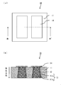
- FIG. 1A is an excerpt of a circuit board in the electronic device shown in FIG. 1
- FIG. 1B is a cross-sectional view taken along line A-A ′ in FIG.
- the other example of the circuit board of this embodiment is shown, (a) is a plan view, (b) is a cross-sectional view taken along line B-B 'of (a).
- FIG. 1 is a cross-sectional view showing an example of an electronic device including the circuit board of the present embodiment.
- the electronic device 1 of the present embodiment includes a through conductor 13 made of metal in the thickness direction of the ceramic sintered body 11 (the through hole 12 penetrating in the drawing and the through conductor 13 on the one main surface side of the ceramic sintered body 11.
- the circuit board 10 is provided with a metal wiring layer 14 connected so as to cover the surface of the substrate 10. On the metal wiring layer 14 constituting the circuit board 10, for example, electrode pads 16 are provided.
- the electronic component 15 is mounted on the electrode pad 16 and is electrically joined by the bonding wire 17 to obtain the electronic device 1 of the present embodiment.
- examples of the electronic component 15 include an insulated gate bipolar transistor (IGBT) element, an intelligent power module (IPM) element, a metal oxide film field effect transistor (MOSFET) element, and a light emitting diode (LED) element.
- IGBT insulated gate bipolar transistor
- IPM intelligent power module
- MOSFET metal oxide film field effect transistor
- LED light emitting diode
- Semiconductor elements such as freewheeling diode (FWD) element, giant transistor (GTR) element, Schottky barrier diode (SBD), heating element for sublimation type thermal printer head or thermal inkjet printer head, Peltier element, etc. Can be used.
- FIG. 2A and 2B show an excerpt of the circuit board 10 in the electronic device shown in FIG. 1, wherein FIG. 2A is a plan view and FIG. 2B is a cross-sectional view taken along line A-A ′ of FIG.
- FIG. 2A is a plan view
- FIG. 2B is a cross-sectional view taken along line A-A ′ of FIG.
- the circuit board 10 of the present embodiment includes a through conductor 13 made of metal in a through hole 12 that penetrates in the thickness direction of the ceramic sintered body 11, and includes at least the ceramic sintered body 11.
- a metal wiring layer 14 is provided so as to cover the surface of the through conductor 13 on the main surface side, and the through conductor 13 is formed on the inner wall side of the through hole 12 along the thickness direction of the ceramic sintered body 11. Having a first region 13a located from one end to the other end and a second region 13b adjacent to the first region 13a, the average crystal grain size in the second region 13b being the first region 13a. It is characterized by being larger than the average crystal grain size.
- the diameter of the through hole 12 is increased. Since the metal paste having a large crystal grain size is present on the center side of the through hole 12, the shrinkage of the metal paste during firing on the center side of the diameter of the through hole 12 is small, so that the depression of the through conductor 13 can be reduced. it can.
- the depression of the metal wiring layer 14 connected to cover the surface of the through conductor 13 can be reduced, and when an electronic component (not shown) is mounted on the metal wiring layer 14 via the electrode pad, It is possible to reduce the occurrence of problems such as the contact area being reduced and the heat dissipation characteristics being lowered, or the electrode pad being detached and not functioning as an electronic device. Further, since the second region 13b having a large average crystal grain size is provided on the center side of the diameter of the through hole 12, it is generated when an electronic component (not shown) transmitted to one end side of the through hole 12 is operated. Heat can be transferred to the other end side quickly, so that the heat dissipation characteristics can be improved.
- the first region 13a having a small average crystal grain size is provided on the inner wall side of the through hole 12, whereby the through conductor 13 in the through hole 12 is provided.
- the bonding strength of can be made high.
- the first region 13a and the second region 13b are, for example, the center of the diameter of the through hole 12 in the cross-sectional view shown in FIG. From the center to the inner wall of the through-hole 12, the portion corresponding to 4/5 of the radius from the center is the second region 13b, and the portion corresponding to the inner wall side other than the second region 13b is the first region 13a.
- the diameter (diameter) of the through hole 12 is 130 ⁇ m (65 ⁇ m in radius)
- a portion corresponding to a circle having a radius of 52 ⁇ m from the center of the diameter of the through hole 12 toward the inner wall is the second region 13b.
- the portion corresponding to the inner wall side other than the second region 13b is the first region 13a.
- the through conductor 13 is cut in the thickness direction of the ceramic sintered body 11, and the ceramic firing is performed using a cross section polisher (CP). What is necessary is just to confirm the surface grind
- any five points of the first region 13a and the second region 13b are selected.
- the crystal grain size may be obtained for each observation image using image analysis software, and the average crystal grain size may be calculated from the value of each crystal grain size.
- the depression of the metal wiring layer 14 connected to cover the surface of the through conductor 13 can be measured by using a surface roughness meter or a laser displacement meter.
- a surface roughness meter or a laser displacement meter For example, when measuring with a laser displacement meter, the surface of the metal wiring layer 14 located where the surface of the through conductor 13 is not covered and the metal wiring layer 14 located where the surface of the through conductor 13 is covered It is only necessary to measure several points on the surface and set the difference between the maximum value and the minimum value of the measured value as the value of the depression.
- the circuit board 10 of the present embodiment it is preferable that particles having a crystal grain size of 4% or more and 10% or less of the minimum diameter of the through hole 12 are present in the second region 13b by 50 area% or more.
- particles having a crystal grain size of 4% or more and 10% or less of the minimum diameter of the through hole 12 are present in the second region 13b by 50 area% or more.
- the dent can be reduced and the through hole can be reduced. Heat generated during operation of the electronic component transmitted to one end side of 12 can be transferred to the other end side more quickly, and heat dissipation characteristics can be improved.
- the area occupancy of the particles having a crystal grain size of 4% or more and 10% or less of the minimum diameter of the through-hole 12 is, for example, the same as in the calculation of the average crystal grain size. What is necessary is just to calculate the area occupation rate of the crystal grain diameter of 4% or more and 10% or less of the minimum diameter of the through hole 12 in the second region 13b by using image analysis software.
- the average crystal grain size in the second region 13b is preferably 3.1% to 5.8% of the minimum diameter of the through hole 12.
- the through conductor constituting the circuit board 10 of the present embodiment in the 13th second region 13b, voids having an average diameter of 1% or more and 4% or less of the minimum diameter of the through hole 12 are present in a range of 3% by area or more and 5% by area or less.
- the voids present in the second region 13b contribute to reducing the depression of the through conductor 13 without reducing the thermal conductivity.
- the binarization process is performed on the observed image using image analysis software, as in the calculation of the average crystal grain size.
- the voids may be extracted by calculating the average void diameter and void ratio.
- the average crystal grain size in the first region 13a is preferably 1.5% or more and less than 4% of the minimum diameter of the through hole 12.
- the bonding strength of the through conductor 13 in the through hole 12 can be increased, Also in the first region 13b, heat generated during operation of the electronic component transmitted to one end side of the through hole 12 can be quickly transferred to the other end side.
- the average crystal grain size in the second region 13b is larger than the average crystal grain size in the metal wiring layer 14.
- the heat flow generated during the operation of the electronic component 15 causes the second flow of the through conductor 13 from the metal wiring layer 14. Therefore, the heat dissipation characteristics can be improved.
- the metal wiring layer 14 is cut in the thickness direction of the ceramic sintered body 11, and polished by using a cross section polisher (CP). Next, confirm using SEM at a magnification of 5000 times, select and observe any five points, determine the crystal grain size using image analysis software for each observation image, and average from the value of each crystal grain size What is necessary is just to calculate a crystal grain size.
- the through conductor 13 contains glass, and the glass content in the second region 13b is larger than the glass content in the first region 13a.
- the thermal expansion of the second region 13b having a high occupied volume ratio of the through conductor 13 can be reduced. Therefore, the shape change of the through conductor 13 during the cooling cycle when the electronic component 15 is repeatedly activated and stopped is reduced, and it is possible to make it difficult for the through hole 12 and the through conductor 13 to be peeled off.
- the glass content in the first region 13a and the second region 13b is measured by, for example, cutting the through conductor 13 in the thickness direction of the ceramic sintered body 11 and using a cross section polisher (CP).
- the polished surface is taken as the measurement surface.
- the boundary between the first region 13a and the second region 13b is confirmed by the method described above, and each of the first region 13a and the second region 13b is subjected to EDS (energy dispersive X-type) attached to the SEM.
- EDS energy dispersive X-type
- the through conductor 13 contains glass containing Bi.
- the through conductor 13 contains Bi-containing glass, the wettability with the ceramic sintered body 11 is good, so that the bonding strength of the through conductor 13 in the through hole 12 can be made higher. This is based on the fact that a large amount of Bi is present at the interface with the inner wall of the through hole 12 when the bonding strength of the through conductor 13 in the through hole 12 is high.
- the glass containing Bi include SiO 2 —B 2 O 3 —Bi 2 O 3 glass and R 2 O—SiO 2 —B 2 O 3 —Bi 2 O 3 glass (R: alkali metal).
- the Bi may be confirmed using, for example, a TEM (transmission electron microscope) or an EDS attached to the SEM.
- the thickness of the glass is, for example, not less than 0.5 ⁇ m and not more than 5.0 ⁇ m.
- FIG. 3A and 3B show another example of the circuit board of the present embodiment, in which FIG. 3A is a plan view and FIG. 3B is a cross-sectional view taken along line B-B ′ in FIG.
- the circuit board 10 in FIG. 3 is open on the other main surface rather than the opening area of the through hole 12 opened on one main surface (surface on which electronic components are mounted) of the ceramic sintered body 11.
- the opening area of the through hole 12 is large, an example in which the diameter of the through hole 12 increases from one main surface to the other main surface is shown.
- the opening area of the through-hole 12 that opens to the other main surface is larger than the opening area of the through-hole 12 that opens to one main surface of the ceramic sintered body 11, one end of the through-hole 12 Since heat generated during operation of an electronic component (not shown) transmitted to the side can be efficiently dissipated on the other end side, heat dissipation characteristics can be further enhanced.
- the ceramic sintered body 11 constituting the circuit board 10 of the present embodiment includes an aluminum oxide sintered body, a zirconium oxide sintered body, a silicon nitride sintered body, an aluminum nitride sintered body, or a mullite quality.
- One kind selected from the sintered bodies or a mixed sintered body can be used.
- the main component of the through conductor 13 is copper
- the ceramic sintered body 11 is an aluminum oxide sintered body or an aluminum nitride sintered body, the interface between the inner wall of the through hole 12 and the through conductor 13 is used.
- the ceramic sintered body 11 is preferably made of an aluminum oxide sintered body.
- the through conductor 13 constituting the circuit board 10 of the present embodiment is preferably composed mainly of copper, silver or aluminum, and particularly preferably composed mainly of copper.
- the through conductor 13 is mainly composed of copper, the heat dissipation characteristics can be enhanced because copper has high thermal conductivity.
- the metal paste used as the through conductor 13 is composed mainly of copper and contains a glass having a softening point of 600 ° C. or higher and 700 ° C. or lower, by firing at a temperature near the melting point of copper, high bonding can be achieved. Strength can be obtained.
- the main component of the through conductor 13 refers to a component exceeding 50 mass% of the components constituting the through conductor 13.
- the metal wiring layer 14 constituting the circuit board 10 of the present embodiment is preferably composed mainly of copper, silver or aluminum, and more preferably composed mainly of copper, like the through conductor 13.
- the metal wiring layer 14 may be subjected to a plating process on the exposed surface of the metal wiring layer 14 partially or entirely.
- the type of plating may be any known plating, and examples thereof include gold plating, silver plating, nickel-gold plating, and the like.
- the through hole 12 is formed by micro drilling, sand blasting, micro blasting, laser processing, or the like.
- a method for forming the through hole 12 there is little generation of burrs and chips, and it is possible to freely change the shape of the through hole 12 in the thickness direction of the ceramic sintered body 11 by changing the oscillation output. Therefore, it is preferable to carry out by laser processing.
- a metal paste to be the through conductor 13 is prepared.
- This metal paste contains metal powder, glass powder, and an organic vehicle. Moreover, you may add a metal oxide as needed.
- the metal powder for example, a metal powder having an average particle size of less than 1 ⁇ m, a metal powder of 1 to 3 ⁇ m, and a metal powder of 3 to 10 ⁇ m are used.
- the sinterability of the through conductors 13 can be improved due to the presence of metal powders having a small average particle diameter and less than 1 ⁇ m.
- the thermal conductivity can be enhanced by the presence of a metal powder having a large average particle diameter of 3 ⁇ m or more and less than 10 ⁇ m.
- a compounding ratio of the first metal powder contained in the metal paste to be the first region 13a for example, metal powder having an average particle diameter of less than 1 ⁇ m out of a total of 100 mass% of the first metal powder. Is 40 mass% or more and 65 mass% or less, and the metal powder of 1 ⁇ m or more and less than 3 ⁇ m is 20 mass% or more and 45 mass% or less, and the metal powder of 3 ⁇ m or more and less than 10 ⁇ m is 10 mass% or more and 35 mass% or less.
- the metal powder whose average particle diameter is less than 1 micrometer among total 100 mass% of 2nd metal powder for example.
- the glass powder is not particularly limited, but it is preferable to use a glass powder having a softening point of 400 ° C. or higher and 700 ° C. or lower.
- the softening point is 600 ° C. or more and 700 ° C. or less, crystal grain growth can be prevented when the metal powder is sintered in firing, the crystal grain size can be reduced, and the penetration in the through hole 12 The bonding strength of the conductor 13 can be improved.
- the glass examples include SiO 2 type, R 2 O—SiO 2 type (R: alkali metal element), SiO 2 —B 2 O 3 type, R 2 O—SiO 2 —B 2 O 3 type, Examples thereof include SiO 2 —B 2 O 3 —Bi 2 O 3 system, R 2 O—SiO 2 —B 2 O 3 —Bi 2 O 3 system, and the like.
- glass containing Bi is preferably used in terms of improving the bonding strength between the inner wall of the through hole 12 and the through conductor 13.
- the organic vehicle is obtained by dissolving an organic binder in an organic solvent.
- the ratio of the organic binder to the organic solvent is 2 to 6 with respect to the organic binder 1.
- the organic binder include acrylics such as polybutyl methacrylate and polymethyl methacrylate, celluloses such as nitrocellulose, ethyl cellulose, cellulose acetate, and butyl cellulose, polyethers such as polyoxymethylene, polybutadiene, and polyisoprene. 1 type or 2 types or more selected from these polyvinyls can be used.
- the organic solvent is selected from, for example, carbitol, carbitol acetate, terpineol, metacresol, dimethylimidazole, dimethylimidazolidinone, dimethylformamide, diacetone alcohol, triethylene glycol, paraxylene, ethyl lactate, and isophorone. 1 type or 2 types or more can be mixed and used.
- the compounding ratio of the metal powder, glass powder, and organic vehicle used as the metal paste is 77.0% by mass to 87.0% by mass of the metal powder and 0.5% by mass to 5% by mass of the glass powder out of 100% by mass of the metal paste. %, And the organic vehicle is preferably in the range of 10% by mass to 20% by mass.
- the viscosity is preferably 0.8 Pa ⁇ s or more and 1.3 Pa ⁇ s or less.
- the ceramic sintered body 11 is an aluminum oxide sintered body or an aluminum nitride sintered body, it is preferably copper oxide (CuO or Cu 2 O). .
- copper oxide which is a metal oxide
- copper aluminate CuAl 2 O 4 or CuAlO 2
- the bonding strength can be further increased.
- the ceramic sintered body 11 is an aluminum oxide sintered body
- the metal oxide contained in the metal paste is aluminum oxide (Al 2 O 3 )
- the through conductor 13 formed by firing the metal paste if the metal oxide contained in the metal paste is aluminum oxide (Al 2 O 3 ), the through conductor 13 formed by firing the metal paste.
- the thermal expansion coefficient of the aluminum oxide sintered body can be made closer to that of the aluminum oxide sintered body, and problems such as peeling of the joint due to the difference in thermal expansion coefficient between the ceramic sintered body 11 and the through conductor 13 can be reduced. Can do.
- the first metal paste, the second metal powder, the glass powder, and the organic vehicle that become the first region 13a are used to form the second region.
- a second metal paste to be the region 13b is produced.
- the inside of the through hole 12 is filled into the through hole 12 using a nozzle capable of simultaneously filling the first metal paste on the inner wall side of the through hole 12 and the second metal paste on the center side of the diameter of the through hole 12.
- the abundance of the glass in the first region 13a and the second region 13b can be adjusted by changing the compounding ratio of the glass powder in the first metal paste and the second metal paste.
- the metal paste filled in the through holes 12 is dried at 80 ° C. or higher and 150 ° C. or lower. If it is this temperature range, the void which contributes to reducing a hollow can be formed, without the organic component in a metal paste volatilizing abundantly, without reducing a thermal radiation characteristic.
- the metal powder constituting the metal paste is copper
- the maximum temperature is 850 ° C. or more and 1050 ° C. or less
- the maximum temperature is 800 ° C. or more and 1000 ° C. or less
- the maximum temperature is 500 ° C. or more and 600 ° C.
- the following firing is performed with a holding time of 0.5 hours or more and 3 hours or less. Note that the firing atmosphere is performed in a non-oxidizing atmosphere to suppress oxidation of the metal paste.
- the metal wiring layer 14 is formed on the surface of the through conductor 13 on the one main surface side of the ceramic sintered body 11.
- the metal paste used to form the metal wiring layer 14 may be one having excellent conductivity and thermal conductivity, but if the same metal paste as any of the metal pastes used as the through conductors 13 is used, the manufacturing process will be In addition to simplification, since there is no difference in thermal expansion coefficient between the through conductor 13 and the metal wiring layer 14, cracks and the like are less likely to occur during sintering.
- the metal wiring layer 14 can be produced by printing a metal paste using a known screen printing method, and then drying and firing.
- the thickness of the metal wiring layer 14 is preferably 40 ⁇ m or more. If the thickness of the metal wiring layer 14 is 40 ⁇ m or more, excellent heat dissipation characteristics can be exhibited while having conductivity. Further, the metal wiring layer 14 may be repeatedly formed until it has a desired thickness by performing printing, drying, and baking in several times. Needless to say, the metal wiring layer 14 may be formed on the surface of the through conductor 13 on the other main surface side of the ceramic sintered body 11 to further improve the heat dissipation characteristics.
- the metal wiring layer 14 after printing and drying and baking a metal paste to a portion outside the necessary area of the metal wiring layer 14, a resist film is formed in the necessary area of the metal wiring layer 14, and chlorinated. Etching with an etching solution made of ferric, cupric chloride or alkali, etc., and then removing the resist film with an aqueous sodium hydroxide solution, etc., to produce the metal wiring layer 14 in the necessary region Also good.
- the thickness is preferably 100 ⁇ m or less.
- the through-hole 12 penetrating in the thickness direction of the ceramic sintered body 11 is provided with the through-conductor 13 made of metal, and the surface of the through-conductor 13 on at least one main surface side of the ceramic sintered body 11 is covered.
- a circuit board 10 having a metal wiring layer 14 connected thereto, the through conductor 13 extending from one end of the through hole 12 to the other end along the thickness direction of the ceramic sintered body 11 on the inner wall side of the through hole 12
- the first region 13a is positioned and the second region 13b is adjacent to the first region 13a, and the average crystal grain size in the second region is larger than the average crystal grain size in the first region.
- the circuit board 10 can be obtained.
- the manufacturing method of the circuit board 10 of the present embodiment is not limited to the manufacturing method described above.
- the circuit board 10 can be efficiently manufactured by forming a large number of the circuit boards 10 according to the present embodiment by the above-described method using the ceramic sintered body 11 in which the division grooves are formed, and then dividing the circuit board 10. .
- the electronic device 1 of this embodiment can be obtained.
- the electronic device 1 of the present embodiment can be a highly reliable electronic device 1 that can be used for a long period of time by mounting the electronic component 15 on the circuit board 10 of the present embodiment.
- the electronic component 15 is provided on the surface of the through conductor 13 on the one main surface side of the ceramic sintered body 11 via the metal wiring layer 14 or the like. Preferably it is located.
- Samples with different average crystal grain sizes in the first region 13a and the second region 13b were prepared, and tests on the depression of the through conductor 13, heat dissipation characteristics, and reliability were performed.
- an aluminum oxide sintered body having an aluminum oxide content of 96% by mass was prepared using silicon oxide and magnesium oxide as sintering aids.
- the ceramic sintered body 11 was grooved so that a large number of samples could be taken.
- the ceramic sintered body 11 was subjected to laser processing to form a through hole 12 having a diameter of 130 ⁇ m from one end to the other end.
- the metal paste used for the preparation of each sample is made of copper, and the average crystal grain size shown in Table 2 is obtained by changing the mixing ratio of metal powders having average grain sizes of 0.5 ⁇ m, 2 ⁇ m, and 6 ⁇ m. 86% by mass of the mixed metal powder, 3% by mass of R 2 O—SiO 2 —B 2 O 3 glass powder, and 11% by mass as an organic vehicle (organic binder: 2.5% by mass of acrylic resin) Organic solvent: ⁇ -terpineol was 8.5% by mass, and the ratio of ⁇ -terpineol to acrylic resin was 3.4).
- the first metal paste and the second metal paste were prepared.
- the viscosity of each metal paste was in the range of 0.8 Pa ⁇ s to 1.3 Pa ⁇ s.
- sample No. 1 was formed so as to be the metal wiring layer 14 covering the surface of the through conductor 13 on one main surface of the ceramic sintered body 11 and contacting the through conductor 13. Screen printing was performed using the same metal paste as the second metal paste of No. 2.
- the metal wiring layer 14 was formed to have a thickness of 40 ⁇ m. Then, after drying at 100 ° C. in an air atmosphere, the through conductor 13 and the metal wiring layer 14 were fired at a firing temperature of 900 ° C. and a firing time of 1 hour in a nitrogen atmosphere in which the oxygen concentration was adjusted to 5 ppm. And sample no. 1-18 were obtained.
- a part of each sample is cut and polished using a cross section polisher (CP) so that the cut line of the diameter of the through hole 12 opened in the ceramic sintered body 11 becomes a cross section, and then known.
- the cross section of the through conductor 13 was etched using an etching solution.
- SEM scanning electron microscope
- an arbitrary five points of each of the first region 13a and the second region 13b are selected and observed at a magnification of 5000 times, and image analysis software is used for each observation image.
- the crystal grain size was determined by using it, and the average crystal grain size was calculated from the value of each crystal grain size. Further, the ratio of the average crystal grain size with respect to the minimum diameter of 130 ⁇ m of the through hole 12 was calculated. Further, the area occupancy of the crystal grain size of 4% to 10% of the minimum diameter of the through hole 12 in the second region 13b of the through conductor 13 was calculated for the observed image using image analysis software.
- thermography manufactured by JEOL Ltd., model number: JTG-7200
- the average crystal grain size in the first region 13a is larger than the average crystal grain size in the second region 13b, or the average crystal grain size in the first region 13a and the average in the second region 13b.
- Sample No. with the same crystal grain size. 17 and 18 had a depression of 14.7 ⁇ m or more, a surface temperature of 78.2 ° C. or more, and a cycle number of 2050 or less.
- the sample No. 1 in which the average crystal grain size in the second region 13b is larger than the average crystal grain size in the first region 13a is larger than the average crystal grain size in the first region 13a.
- the indentation was 12 ⁇ m or less
- the surface temperature was 72 ° C. or less
- the number of cycles was 2200 or more, indicating that the circuit board was excellent in heat dissipation characteristics and reliability.
- a sample No. 4 in which particles having a crystal grain size of 4% or more and 10% or less of the minimum diameter of the through-hole 12 exist in an amount of 50 area% or more.
- Nos. 6 to 16 were found to be excellent circuit boards, with the results that the depression was 9.2 ⁇ m or less, the surface temperature was 67.4 ° C. or less, and the number of cycles was 2500 or more.
- Sample No. whose average crystal grain size in the first region 13a is 1.5% or more and less than 4% of the minimum diameter of the through hole 12 is obtained.
- the pits were 8.4 ⁇ m or less, the surface temperature was 64.4 ° C. or less, and the number of cycles was 2750 or more, indicating that they were further excellent circuit boards.
- sample No. 1 in Example 1 was used.
- the metal wiring layer 14 was formed by using the metal paste used for forming the second region 13b in 4, 8, and 14.
- the structure of the metal wiring layer 14 is the same as that of the sample No. 1 of Example 1.
- 4 is the same as the second region 13b of Sample 4.
- sample No. 14 is the same as Sample No. 14.
- Sample No. 8 is the same as Sample No. 8. 21.
- Sample No. 19 is Sample No.
- the number of cycles exceeds 20 and 21, and the average crystal grain size in the second region 13b is made larger than the average crystal grain size in the metal wiring layer 14, so that the operation of the electronic component 15 is achieved. It was found that the heat flow sometimes generated smoothly flows from the metal wiring layer 14 to the second region 13b of the through conductor 13, thereby improving the heat dissipation characteristics.
- samples in which the glass content in the first region 13a and the glass content in the second region 13b were made different were prepared, and tests on heat dissipation characteristics and reliability were performed.
- the mixing ratio of the second metal paste was changed, and sample No. No. 22 is 2.0% by weight of glass powder, sample no. No. 23 is 3.0% by mass of glass powder, sample no. 24 changed the glass powder to 4.0% by mass.
- the amount of organic vehicle added was increased or decreased while the ratio of terpineol to acrylic resin was fixed at 3.4 by the amount of increase or decrease in glass powder.
- Example 1 The glass content in the first region 13a and the second region 13b is measured by first cutting the through conductor 13 in the thickness direction of the ceramic sintered body 11 and using a cross section polisher (CP). The polished surface was used as the measurement surface. Next, the first region 13a and the second region 13b were confirmed at a magnification of 2000 using an EDS attached to the SEM, and arbitrary five points were selected and observed. Then, the glass content of each observation image was calculated using image analysis software, and the average value was calculated as the glass content in the first region 13a and the second region 13b. The results are shown in Table 3.
- Sample No. 24 is Sample No.
- the number of cycles exceeded that of 22 and 23, and the glass content in the second region 13b was made higher than the glass content in the first region 13a. Since the thermal expansion of the second region 13b having a high occupied volume ratio can be mitigated, it is possible to reduce the shape change of the through conductor 13 during the cooling cycle when the electronic component 15 is repeatedly activated and stopped. It has been found that the peeling between the through hole 12 and the through conductor 13 can be made difficult to occur.
- a sample prepared using a metal paste to which glass containing Bi was added (hereinafter referred to as a sample with Bi) and a sample prepared using a metal paste to which glass not containing Bi was added (hereinafter referred to as Bi-free sample).
- a heat cycle test was conducted.
- the manufacturing method and the test method were carried out except that R 2 O—SiO 2 —B 2 O 3 system or R 2 O—SiO 2 —B 2 O 3 —Bi 2 O 3 system was used as the glass powder.
- the interface between the inner wall of the through-hole 12 and the through-conductor 13 was observed with a TEM, and the presence of Bi was confirmed for a sample manufactured using a metal paste to which glass containing Bi was added.
- the sample with Bi shows an improvement of 10% in terms of the number of cycles compared to the sample without Bi, and because it contains glass containing Bi, the inner wall of the through hole 12 and the through conductor 13 It has been found that the bonding strength can be increased, and a highly reliable circuit board can be obtained in which the through conductor 13 is hardly peeled off due to repeated heat.
- Sample No. Sample no. 26 and 27 have an opening area of the through hole 12 opened on the other main surface, rather than an opening area of the through hole 12 opened on the one main surface of the ceramic sintered body 11 on which the electronic component 15 is mounted. Since it is large, it was found that the circuit board can be further improved in heat dissipation characteristics and heat dissipation characteristics.
- Circuit board 11 Ceramic sintered body 12: Through hole 13: Through conductor 13a: First region 13b: Second region 14: Metal wiring layer 15: Electronic component 16: Electrode pad
Landscapes
- Engineering & Computer Science (AREA)
- Microelectronics & Electronic Packaging (AREA)
- Chemical & Material Sciences (AREA)
- Ceramic Engineering (AREA)
- Inorganic Chemistry (AREA)
- Printing Elements For Providing Electric Connections Between Printed Circuits (AREA)
- Parts Printed On Printed Circuit Boards (AREA)
- Structure Of Printed Boards (AREA)
Abstract
【課題】 接合強度が高く、放熱特性に優れているとともに、貫通導体上に形成される金属配線層の窪みを小さくすることによって、長期間にわたって使用可能な信頼性の高い回路基板およびこの回路基板に電子部品を搭載してなる電子装置を提供する。 【解決手段】 セラミック焼結体11の厚み方向に貫通する貫通孔12に金属からなる貫通導体13を備えるとともに、セラミック焼結体11の少なくとも一方主面側の貫通導体13の表面を覆って接続されている金属配線層14を備えた回路基板10であって、貫通導体13は、貫通孔12の内壁側にセラミック焼結体11の厚み方向に沿って貫通孔12の一端から他端にかけて位置する第1の領域13aと、第1の領域13aに隣接する第2の領域13bとを有し、第2の領域13bにおける平均結晶粒径が、第1の領域13aにおける平均結晶粒径よりも大きい回路基板10である。
Description
本発明は、回路基板およびこの回路基板に電子部品を搭載してなる電子装置に関するものである。
回路基板上に接合された金属配線層等を介して、半導体素子、発熱素子、ペルチェ素子等の各種電子部品が搭載された電子装置が用いられている。そして、これらの電子部品は作動時に熱を生じるものであり、近年の電子部品の高集積化、電子装置の小型化や薄型化によって、回路基板の体積当たりに加わる熱量は大きくなっていることから、接合が剥がれないことに加えて、放熱特性の高い回路基板が求められている。
そのため、回路基板を構成する支持基板において、電子部品の直下にあたる部位に貫通孔を形成し、この貫通孔内に設けた導体(以降、貫通導体と記載する。)を利用して放熱特性を向上させることが行なわれている。しかし、貫通導体の形成を、金属めっきで埋める場合には、貫通孔の内壁から金属めっきが成長することから、貫通導体の表面中央に窪みが生じる。また、金属ペーストを充填する場合にも、焼成する際の収縮によって貫通導体の表面中央に窪みが生じる。そして、この貫通導体の表面を覆って形成される金属配線層は、貫通導体の表面性状に倣った表面性状となることから、金属配線層の表面にも窪みを生じることとなり、金属配線層上に電極パッド等を介して電子部品を搭載したとき、各部材間において接合不良が生じたり、接合面積が少なく放熱特性が低下したりするという問題があった。
このような、問題を解決すべく、例えば、特許文献1には、セラミック基板に形成されたスルーホールに充填した後、焼成するための導体ペーストであって、金属粉末を主成分とする導電粉末と、膨張剤と、展色剤と、を含む無収縮性スルーホール充填用導体ペーストが提案されている。
しかしながら、特許文献1に記載された無収縮性スルーホール充填用導体ペーストを使用して作製された回路基板の場合、貫通導体の焼成時の収縮性は改善できるものの、膨張剤の熱伝導性は低いものであるため、放熱特性の高い回路基板とすることはできなかった。
本発明は、接合強度が高く、放熱特性に優れているとともに、貫通導体上に形成される金属配線層の窪みを小さくすることによって、長期間にわたって使用可能な信頼性の高い回路基板およびこの回路基板に電子部品を搭載してなる電子装置を提供するものである。
本発明の回路基板は、セラミック焼結体の厚み方向に貫通する貫通孔に金属からなる貫通導体を備えるとともに、前記セラミック焼結体の少なくとも一方主面側の前記貫通導体の表面を覆って接続されている金属配線層を備えた回路基板であって、前記貫通導体は、前記貫通孔の内壁側に前記セラミック焼結体の厚み方向に沿って前記貫通孔の一端から他端にかけて位置する第1の領域と、該第1の領域に隣接する第2の領域とを有し、該第2の領域における平均結晶粒径が、前記第1の領域における平均結晶粒径よりも大きいことを特徴とするものである。
また、本発明の電子装置は、上記構成の本発明の回路基板の金属配線層上に電子部品を搭載してなることを特徴とするものである。
本発明の回路基板は、貫通孔の径の中心側に、大きい結晶粒径の金属粒子が存在していることにより、貫通孔の径の中心側の焼成時の金属ペーストの収縮が小さいので、貫通導体の窪みを小さくすることができる。また、平均結晶粒径の大きい第2の領域を貫通孔の径の中心側に有していることにより、貫通孔の一端側に伝わった電子部品の作動時に生じた熱を、素早く他端側に伝えることができるので放熱特性を高めることができる。さらに、貫通孔の内壁側にセラミック焼結体の厚み方向に沿って貫通孔の一端から他端にかけて平均結晶粒径の小さい第1の領域が位置していることから、貫通導体の接合強度を高いものとすることができる。
また、本発明の電子装置によれば、本発明の回路基板の金属配線層上に電子部品を搭載してなることにより、信頼性の高い電子装置とすることができる。
以下、本実施形態の一例について図面を参照しながら説明する。
図1は、本実施形態の回路基板を備える電子装置の一例を示す断面図である。本実施形態の電子装置1は、セラミック焼結体11の厚み方向(図に貫通する貫通孔12に金属からなる貫通導体13を備えるとともに、セラミック焼結体11の一方主面側の貫通導体13の表面を覆って接続されている金属配線層14を備えた回路基板10を備えているものである。そして、この回路基板10を構成する金属配線層14上に、例えば、電極パッド16を設け、この電極パッド16上に電子部品15を実装し、ボンディングワイヤ17によって電気的に接合することにより、本実施形態の電子装置1となる。
ここで、電子部品15としては、例えば、絶縁ゲート・バイポーラ・トランジスタ(IGBT)素子、インテリジェント・パワー・モジュール(IPM)素子、金属酸化膜型電界効果トランジスタ(MOSFET)素子、発光ダイオード(LED)素子、フリーホイーリングダイオード(FWD)素子、ジャイアント・トランジスタ(GTR)素子、ショットキー・バリア・ダイオード(SBD)等の半導体素子、昇華型サーマルプリンタヘッドまたはサーマルインクジェットプリンタヘッド用の発熱素子、ペルチェ素子等を用いることができる。
次に、本実施形態の回路基板10について図面を用いて説明する。図2は、図1に示す電子装置における回路基板10を抜粋して示す、(a)は平面図であり、(b)は(a)のA-A’線における断面図である。なお、以降の図において、同一の部材については図1と同一の符号を用いて説明するものとする。
本実施形態の回路基板10は、図2に示す例のように、セラミック焼結体11の厚み方向に貫通する貫通孔12に金属からなる貫通導体13を備えるとともに、セラミック焼結体11の少なくとも一方主面側の貫通導体13の表面を覆って接続されている金属配線層14を備え、貫通導体13は、貫通孔12の内壁側にセラミック焼結体11の厚み方向に沿って貫通孔12の一端から他端にかけて位置する第1の領域13aと、第1の領域13aに隣接する第2の領域13bとを有し、第2の領域13bにおける平均結晶粒径が、第1の領域13aにおける平均結晶粒径よりも大きいことを特徴としている。
このように、貫通孔12の径の中心側に、平均結晶粒径の大きい第2の領域13bを有している、すなわち、金属ペーストを焼成させてなる貫通導体13において、貫通孔12の径の中心側に、大きい結晶粒径の金属粒子が存在していることにより、貫通孔12の径の中心側の焼成時の金属ペーストの収縮が小さいので、貫通導体13の窪みを小さくすることができる。そのため、貫通導体13の表面を覆って接続されている金属配線層14の窪みも小さくすることができ、金属配線層14上に電極パッドを介して電子部品(図示せず)を搭載したとき、接触面積が少なくなって放熱特性が低下したり、電極パッドが外れて電子装置としての機能を果たさない等の不具合が起きることを少なくすることができる。さらに、平均結晶粒径の大きい第2の領域13bを貫通孔12の径の中心側に有していることにより、貫通孔12の一端側に伝わった電子部品(図示せず)の作動時に生じた熱を、素早く他端側に伝えることができるので放熱特性を高めることができる。
また、第1の領域13aと第2の領域13bとにおいて、平均結晶粒径の小さい第1の領域13aを貫通孔12の内壁側に有していることにより、貫通孔12内における貫通導体13の接合強度を高いものとすることができる。
なお、図2に示す例の回路基板10における貫通導体13において、第1の領域13aおよび第2の領域13bとは、例えば、図2(b)に示す断面図の貫通孔12の径の中心から貫通孔12の内壁までの半径において、中心から半径の4/5に当たる部分が第2の領域13bであり、第2の領域13b以外の内壁側に当たる部分が第1の領域13aである。例えば、貫通孔12の径の大きさ(直径)が130μm(半径で65μm)であるとき、貫通孔12の径の中心から内壁に向けて半径52μmの円に相当する部分が第2の領域13bであり、第2の領域13b以外の内壁側に当たる部分が第1の領域13aである。
そして、第1の領域13aおよび第2の領域13bを確認するためには、例えば、貫通導体13をセラミック焼結体11の厚み方向に切断し、クロスセクションポリッシャー(CP)を用いて、セラミック焼結体11に開口する貫通孔12の直径が断面となるように研磨した面を、SEM(走査型電子顕微鏡)を用いて5000倍の倍率で確認すればよい。また、貫通導体13の第1の領域13aおよび第2の領域13bの平均結晶粒径を確認するためには、それぞれの第1の領域13aおよび第2の領域13bの任意の5点を選択して観察し、各観察画像について画像解析ソフトを用いて結晶粒径を求め、各結晶粒径の値から平均結晶粒径を算出すればよい。
また、貫通導体13の表面を覆って接続されている金属配線層14の窪みは、表面粗さ計やレーザー変位計を用いることで測定することができる。例えば、レーザー変位計で測定するときには、貫通導体13の表面を覆っていないところに位置する金属配線層14の表面と、貫通導体13の表面を覆っているところ位置している金属配線層14の表面について数カ所測定し、測定値の最大値と最小値との差を窪みの値とすればよい。
また、本実施形態の回路基板10において、第2の領域13bに、貫通孔12の最小径の4%以上10%以下の結晶粒径の粒子が50面積%以上存在していることが好ましい。なお、貫通孔12の最小径とは、前述した平均結晶粒径の算出時と同様の研磨した面を、SEMを用いて2000倍の倍率で確認すればよい。そして、第2の領域13bに、貫通孔12の最小径の4%以上10%以下の結晶粒径の粒子が50面積%以上存在しているときには、窪みを小さくすることができるとともに、貫通孔12の一端側に伝わった電子部品の作動時に生じた熱を、より素早く他端側に伝えることができ、放熱特性を高めることができる。
なお、第2の領域13bにおいて、貫通孔12の最小径の4%以上10%以下の結晶粒径の粒子の面積占有率は、例えば、平均結晶粒径の算出時と同様に、観察画像について画像解析ソフトを用いて第2の領域13bにおける貫通孔12の最小径の4%以上10%以下の結晶粒径の面積占有率を算出すればよい。また、第2の領域13bにおける平均結晶粒径は、貫通孔12の最小径の3.1%以上5.8%以下であることが好ましい。
また、第2の領域13bに、貫通孔12の最小径の4%以上10%以下の結晶粒径の粒子が50面積%以上存在しているとき、本実施形態の回路基板10構成する貫通導体13の第2の領域13bには、貫通孔12の最小径の1%以上4%以下の平均径を有するボイドが3面積%以上5面積%以下の範囲で存在する。この第2の領域13bに存在するボイドは、熱伝導性を低下させることなく、貫通導体13の窪みを小さくすることに寄与するものである。
なお、第2の領域13bにおける平均ボイド径およびボイド率を確認するためには、例えば、平均結晶粒径の算出時と同様に、観察画像について画像解析ソフトを用いて2値化処理を行なうことによってボイドを抽出し、平均ボイド径およびボイド率を算出すればよい。
また、本実施形態の回路基板10において、第1の領域13aにおける平均結晶粒径が、貫通孔12の最小径の1.5%以上4%未満であることが好ましい。第1の領域13aにおける平均結晶粒径が、貫通孔12の最小径の1.5%以上4%未満であるときには、貫通孔12内における貫通導体13の接合強度を高いものとすることができるとともに、第1の領域13bにおいても、貫通孔12の一端側に伝わった電子部品の作動時に生じた熱を、素早く他端側に伝えることができる。
また、本実施形態の回路基板10において、第2の領域13bにおける平均結晶粒径が、金属配線層14における平均結晶粒径よりも大きいことが好ましい。第2の領域13bにおける平均結晶粒径が、金属配線層14における平均結晶粒径よりも大きいときには、電子部品15の作動時に生じた熱の流れが、金属配線層14から貫通導体13の第2の領域13bへとスムーズに流れるため、放熱特性を向上させることができる。ここで、金属配線層14の平均結晶粒径を確認するためには、まず、金属配線層14をセラミック焼結体11の厚み方向に切断し、クロスセクションポリッシャー(CP)を用いて研磨する。次に、SEMを用いて5000倍の倍率で確認し、任意の5点を選択して観察し、各観察画像について画像解析ソフトを用いて結晶粒径を求め、各結晶粒径の値から平均結晶粒径を算出すればよい。
なお、セラミック焼結体11の厚み方向に切断した断面において、セラミック焼結体11の表面の延線であり、貫通孔12の開口部を結ぶ線を、貫通導体13と金属配線層14との境界とする。
また、本実施形態の回路基板10において、貫通導体13がガラスを含有しており、第2の領域13bにおけるガラスの含有量が、第1の領域13aにおけるガラスの含有量よりも多いことが好ましい。第2の領域13bにおけるガラスの含有量が、第1の領域13aにおけるガラスの含有量よりも多いときには、貫通導体13の占有体積率の高い第2の領域13bの熱膨張を緩和することができるため、電子部品15の作動と停止を繰り返したときの冷熱サイクルの際の貫通導体13の形状変化が小さくなり、貫通孔12と貫通導体13との接合の剥がれを生じにくくすることができる。
なお、第1の領域13aおよび第2の領域13bにおけるガラスの含有量の測定方法は、例えば、貫通導体13をセラミック焼結体11の厚み方向に切断し、クロスセクションポリッシャー(CP)を用いて研磨した面を測定面とする。次に、上述した方法により、第1の領域13aおよび第2の領域13bの境界を確認し、第1の領域13aおよび第2の領域13bのそれぞれについて、SEMに付設のEDS(エネルギー分散型X線分析装置)を用いて2000倍の倍率で確認し、任意の5点を選択して観察する。そして、各観察画像について画像解析ソフトを用いてガラスの含有量を求め、それぞれ平均値を算出したものを第1の領域13aおよび第2の領域13bにおけるガラスの含有量とすればよい。
また、本実施形態の回路基板10において、貫通導体13が、Biを含むガラスを含有していることが好ましい。貫通導体13が、Biを含むガラスを含有しているときには、セラミック焼結体11との濡れ性が良いので、貫通孔12内における貫通導体13の接合強度をより高いものとすることができる。これは、貫通孔12内における貫通導体13の接合強度が高いものであるとき、Biは、貫通孔12の内壁との界面に多く存在していることに基づく。そして、Biを含むガラスとしては、例えば、SiO2-B2O3-Bi2O3系ガラスやR2O-SiO2-B2O3-Bi2O3系ガラス(R:アルカリ金属)等があり、Biの確認については、例えば、TEM(透過型電子顕微鏡)やSEMに付設のEDSを用いて確認すればよい。ここで、ガラスの厚みは、例えば0.5μm以上5.0μm以下である。
図3は、本実施形態の回路基板の他の例を示す、(a)は平面図であり、(b)は(a)のB-B’線における断面図である。
図3の回路基板10は、セラミック焼結体11の一方主面(電子部品が搭載される側の面)に開口している貫通孔12の開口面積よりも、他方主面に開口している貫通孔12の開口面積が大きい例として、一方主面から他方主面に向かって貫通孔12の径が大きくなっている例を示している。このように、セラミック焼結体11の一方主面に開口している貫通孔12の開口面積よりも、他方主面に開口している貫通孔12の開口面積が大きいときには、貫通孔12の一端側に伝わった電子部品(図示せず)の作動時に生じた熱を他端側で効率よく放熱することができるので、放熱特性をより高めることができる。
また、本実施形態の回路基板10を構成するセラミック焼結体11は、酸化アルミニウム質焼結体、酸化ジルコニウム質焼結体、窒化珪素質焼結体、窒化アルミニウム質焼結体、またはムライト質焼結体から選択される1種もしくは混合焼結体を用いることができる。また、貫通導体13の主成分が銅であるときは、セラミック焼結体11が酸化アルミニウム質焼結体または窒化アルミニウム質焼結体であれば、貫通孔12の内壁と貫通導体13との界面でアルミン酸銅(CuAl2O4またはCuAlO2)が生成されることで、貫通孔12と貫通導体13との接合強度を高くすることができる。なお、貫通孔12の形成など加工性の観点から、セラミック焼結体11が酸化アルミニウム質焼結体からなることが好ましい。
また、本実施形態の回路基板10を構成する貫通導体13は、銅、銀またはアルミニウムを主成分とすることが好ましく、特には銅を主成分とすることが好ましい。貫通導体13が銅を主成分とするときには、銅は熱伝導性が高いため放熱特性を高めることができる。また、貫通導体13となる金属ペーストが、銅を主成分とし、軟化点が600℃以上700℃以下のガラスを含有するものであるとき、銅の融点近傍の温度で焼成することにより、高い接合強度を得ることができる。また、副成分として、ジルコニウム、チタン、モリブデン、スズまたは亜鉛のうち少なくとも1種を含有してもよい。なお、貫通導体13の主成分とは、貫通導体13を構成する成分のうち、50質量%を超える成分のことをいう。
また、本実施形態の回路基板10を構成する金属配線層14は、貫通導体13と同じく、銅、銀またはアルミニウムを主成分とすることが好ましく、特には銅を主成分とすることが好ましい。なお、金属配線層14は、金属配線層14の露出した表面上に部分的もしくは全面にめっき処理を行なってもよい。このように、めっき処理を行なうことによって、電極パッドやボンディングワイヤなどの接合処理がしやすくなり、さらに金属配線層14が酸化腐蝕するのを抑制することができる。めっきの種類としては公知のめっきであればよく、例えば、金めっき、銀めっきまたはニッケル-金めっきなどが挙げられる。
以下、本実施形態の回路基板の製造方法について説明する。
まず、主成分として、酸化アルミニウム(Al2O3)、焼結助剤として、酸化珪素(SiO2)、酸化マグネシウム(MgO)、酸化カルシウム(CaO)等の粉末を用いて公知の方法により酸化アルミニウム質焼結体を作製する。次に、マイクロドリル、サンドブラスト、マイクロブラストおよびレーザー加工などにより、貫通孔12の形成を行なう。なお、貫通孔12の形成方法としては、バリやカケの発生が少なく、発振出力を変えることによりセラミック焼結体11の厚み方向における貫通孔12の形状を自由に変更することが可能であることから、レーザー加工で行なうことが好ましい。
次に、貫通導体13となる金属ペーストを準備する。この金属ペーストは、金属粉末、ガラス粉末、有機ビヒクルを含有する。また、必要に応じて金属酸化物を加えても良い。そして、金属粉末としては、例えば、平均粒径が1μm未満の金属粉末と、1μm以上3μm未満の金属粉末と、3μm以上10μm未満の金属粉末とを用いる。このように、粒径を異ならせた金属粉末を用いれば、平均粒径の小さい1μm未満の金属粉末の存在によって、貫通導体13の焼結性を向上させることができる。また、平均粒径の大きい3μm以上10μm未満の金属粉末の存在によって、熱伝導性を高めることができる。
ここで、第1の領域13aとなる金属ペーストに含有する第1の金属粉末の配合比としては、第1の金属粉末の合計100質量%のうち、例えば、平均粒径が1μm未満の金属粉末が40質量%以上65質量%以下、1μm以上3μm未満の金属粉末が20質量%以上45質量%以下、3μm以上10μm未満の金属粉末が10質量%以上35質量%以下である。
また、第2の領域13bとなる金属ペーストに含有する第2の金属粉末の配合比としては、第2の金属粉末の合計100質量%のうち、例えば、平均粒径が1μm未満の金属粉末が15質量%以上35質量%以下、1μm以上3μm未満の金属粉末が20質量%以上45質量%以下、3μm以上10μm未満の金属粉末が40質量%以上65質量%以下である。
また、ガラス粉末は、特に限定されるものではないが、軟化点が400℃以上700℃以下のものを用いることが好ましい。特に、軟化点が600℃以上700℃以下ならば、焼成において金属粉末が焼結する際に結晶の粒成長を妨げることができ、結晶粒径を小さくすることができ、貫通孔12内における貫通導体13の接合強度を向上させることができる。このガラスの種類としては、例えば、SiO2系、R2O-SiO2系(R:アルカリ金属元素)、SiO2-B2O3系、R2O-SiO2-B2O3系、SiO2-B2O3-Bi2O3系、R2O-SiO2-B2O3-Bi2O3系などが挙げられる。中でも、Biを含むガラスを用いることが貫通孔12の内壁と貫通導体13との接合強度を向上させる点で好ましい。
また、有機ビヒクルは、有機バインダを有機溶剤に溶解したものであり、例えば、有機バインダと有機溶剤との比率は、有機バインダ1に対し、有機溶剤2~6である。そして、有機バインダとしては、例えば、ポリブチルメタクリレート、ポリメチルメタクリレート等のアクリル類、ニトロセルロース、エチルセルロース、酢酸セルロース、ブチルセルロース等のセルロース類、ポリオキシメチレン等のポリエーテル類、ポリブタジエン、ポリイソプレン等のポリビニル類から選択される1種もしくは2種以上を混合して用いることができる。
また、有機溶剤としては、例えば、カルビトール、カルビトールアセテート、テルピネオール、メタクレゾール、ジメチルイミダゾール、ジメチルイミダゾリジノン、ジメチルホルムアミド、ジアセトンアルコール、トリエチレングリコール、パラキシレン、乳酸エチル、イソホロンから選択される1種もしくは2種以上を混合して用いることができる。
そして、金属ペーストとなる、金属粉末、ガラス粉末、有機ビヒクルの配合比としては、金属ペースト100質量%のうち、金属粉末を77.0質量%以上87.0質量%以下、ガラス粉末を0.5質量%以上5質量%以下、有機ビヒクルを10質量%以上20質量%以下の範囲とすることが好ましい。また、貫通孔12へスムーズに金属ペーストを充填するには、粘度が、0.8Pa・s以上1.3Pa・s以下であることが好ましい。
また、金属ペーストに金属酸化物を含有させるときには、セラミック焼結体11が酸化アルミニウム質焼結体または窒化アルミニウム質焼結体であれば、酸化銅(CuOまたはCu2O)であることが好ましい。このように、金属ペーストに金属酸化物である酸化銅を含有しているときには、アルミン酸銅(CuAl2O4またはCuAlO2)が生成されやすくなり、貫通孔12の内壁と貫通導体13との接合強度をさらに高くすることができる。
また、セラミック焼結体11が酸化アルミニウム質焼結体であるとき、金属ペーストに含有される金属酸化物が酸化アルミニウム(Al2O3)であれば、金属ペーストを焼成してなる貫通導体13の熱膨張係数を酸化アルミニウム質焼結体の熱膨張係数に近づけることができ、セラミック焼結体11と貫通導体13との熱膨張係数差によって、接合の剥がれが生じる等の不具合を少なくすることができる。
そして、上述した第1の金属粉末、ガラス粉末、有機ビヒクルを用いて、第1の領域13aとなる第1の金属ペースト、第2の金属粉末、ガラス粉末、有機ビヒクルを用いて、第2の領域13bとなる第2の金属ペーストを作製する。そして、貫通孔12の内壁側に第1の金属ペースト、貫通孔12の径の中心側に第2の金属ペーストを同時に充填可能なノズルを用いて、貫通孔12内に充填する。
なお、第1の金属ペーストおよび第2の金属ペーストにおけるガラス粉末の配合比を異ならせることによって、第1の領域13aと第2の領域13bのガラスの存在量を調整することができる。
次に、貫通孔12に充填した金属ペーストを80℃以上150℃以下で乾燥する。この温度範囲ならば、金属ペースト中の有機成分が多量に揮発することなく、放熱特性を低下させることなく、窪みを少なくすることに寄与するボイドを形成することができる。その後、金属ペーストを構成する金属粉末が銅であるときには、最高温度850℃以上1050℃以下、銀であるときには、最高温度800℃以上1000℃以下、アルミニウムであるときには、最高温度500℃以上600℃以下とし、保持時間0.5時間以上3時間以下で焼成する。なお、この焼成時の雰囲気は、金属ペーストの酸化を抑制すべく非酸化雰囲気で焼成する。
次に、金属配線層14をセラミック焼結体11の一方主面側の貫通導体13の表面に形成する。金属配線層14を形成するために用いる金属ペーストは導電性および熱伝導性に優れたものを用いれば良いが、貫通導体13となるいずれかの金属ペーストと同じ金属ペーストを用いれば、製造工程が簡略化されるとともに、貫通導体13と金属配線層14との熱膨張係数差がないので、焼結の際にクラックなどが起こりにくくなり好ましい。
金属配線層14は、公知のスクリーン印刷法を用いて金属ペーストを印刷した後、乾燥して焼成することによって作製することができる。また、金属配線層14の厚みは40μm以上であることが好ましく、金属配線層14の厚みが40μm以上であれば、導電性を有しつつ優れた放熱特性を示すことができる。また、金属配線層14は、数回に分けて印刷、乾燥、焼成を行なって所望の厚みになるまで繰り返して形成しても良い。また、金属配線層14は、セラミック焼結体11の他方主面側の貫通導体13の表面に形成して放熱特性をさらに向上させてもよいことはいうまでもない。
また、金属配線層14の作製において、金属配線層14の必要領域外となる部分にまで金属ペーストを印刷して乾燥し焼成した後、金属配線層14の必要領域にレジスト膜を形成し、塩化第二鉄、塩化第二銅またはアルカリからなるエッチング液等を用いてエッチングし、その後、水酸化ナトリウム水溶液等を用いてレジスト膜を除去することで、必要領域に金属配線層14を作製してもよい。このように、エッチングにより金属配線層14を作製するときには、厚みは100μm以下であることが好ましい。
以上の手順により、セラミック焼結体11の厚み方向に貫通する貫通孔12に金属からなる貫通導体13を備えるとともに、セラミック焼結体11の少なくとも一方主面側の貫通導体13の表面を覆って接続されている金属配線層14を備えた回路基板10であって、貫通導体13は、貫通孔12の内壁側にセラミック焼結体11の厚み方向に沿って貫通孔12の一端から他端にかけて位置する第1の領域13aと、第1の領域13aに隣接する第2の領域13bとを有し、第2の領域における平均結晶粒径が、第1の領域における平均結晶粒径よりも大きい回路基板10を得ることができる。
また、本実施形態の回路基板10の製造方法は上述した製造方法に限るものではない。なお、回路基板10は、分割溝が形成されたセラミック焼結体11を用いて、上述した方法で本実施形態の回路基板10を多数個形成し、その後分割すれば、効率よく作製可能である。
そして、金属配線層14上に、例えば、電極パッド16を設け、この電極パッド16上に電子部品15を実装することにより、本実施形態の電子装置1とすることができる。この本実施形態の電子装置1は、本実施形態の回路基板10に電子部品15を搭載してなることにより、長期間にわたって使用可能な信頼性の高い電子装置1とすることができる。なお、より放熱特性に優れた電子装置1とするには、セラミック焼結体11の一方主面側の貫通導体13の表面上となる部分に、金属配線層14等を介して電子部品15が位置していることが好ましい。
以下、本発明の実施例を具体的に説明するが、本発明は以下の実施例に限定されるものではない。
第1の領域13aと第2の領域13bとにおける平均結晶粒径を異ならせた試料を作製し、貫通導体13の窪み、放熱特性および信頼性に関する試験を行なった。
まず、酸化珪素および酸化マグネシウムを焼結助剤とし、酸化アルミニウムの含有量が96質量%の酸化アルミニウム質焼結体を作製した。なお、セラミック焼結体11には、試料を多数個取りできるように、溝加工を施した。
そして、セラミック焼結体11に、レーザー加工を施して、一端から他端にかけて直径が130μmの貫通孔12を形成した。次いで、各試料の作製のために使用する金属ペーストについては、銅からなり、平均粒径が0.5μm,2μm,6μmの金属粉末の混合比率を異ならせて表2に示す平均結晶粒径となるように調整した金属混合粉末を86質量%と、R2O-SiO2-B2O3系のガラス粉末を3質量%と、有機ビヒクルとして11質量%(有機バインダ:アクリル樹脂を2.5質量%、有機溶剤:α―テルピネオールを8.5質量%、アクリル樹脂に対するα-テルピネオールの比率3.4)とし、第1の金属ペーストおよび第2の金属ペーストを調合した。各金属ペーストの粘度は、0.8Pa・s以上1.3Pa・s以下の範囲内であった。
次いで、貫通孔12の内壁側に第1の金属ペースト、貫通孔12の径の中心側に第2の金属ペーストを同時に充填可能なノズルを用いて、貫通孔12内に充填した。次いで、セラミック焼結体11の一方主面の貫通導体13の表面を覆って貫通導体13と接する金属配線層14となるように、試料No.2の第2の金属ペーストと同じ金属ペーストを用いてスクリーン印刷を行なった。なお、金属配線層14の厚みは40μmとなるように形成した。そして、大気雰囲気で100℃にて乾燥させた後、酸素濃度を5ppmに調整した窒素雰囲気の中で、焼成温度を900℃、焼成時間を1時間で焼成して貫通導体13および金属配線層14を形成し、試料No.1~18を得た。
次に、各試料の一部を切断し、クロスセクションポリッシャー(CP)を用いて、セラミック焼結体11に開口する貫通孔12の直径の切断線が断面となるように研磨した後、公知のエッチング溶液を用いてこの貫通導体13の断面をエッチングした。その後、SEM(走査型電子顕微鏡)を用いて5000倍の倍率でそれぞれの第1の領域13aおよび第2の領域13bの任意の5点を選択して観察し、各観察画像について画像解析ソフトを用いて結晶粒径を求め、各結晶粒径の値から平均結晶粒径を算出した。また、貫通孔12の最小径130μmに対する平均結晶粒径の比率を算出した。また、観察した画像について画像解析ソフトを用いて、貫通導体13の第2の領域13bにおける貫通孔12の最小径の4%以上10%以下の結晶粒径の面積占有率を算出した。
次に、レーザー変位計を用いて、貫通導体13上に位置していない金属配線層14の表面と、貫通導体13上に位置している金属配線層14の表面について数カ所測定し、測定値の最大値と最小値との差を窪みの値とした。
次に、放熱特性試験として、各試料に電子部品15を搭載し、30Aの電流を流した。そして、電流を流してから5分間放置後に電子部品15の表面温度をサーモグラフィー(日本電子株式会社製、型番:JTG-7200)で測定した。なお、測定距離は20cmとした。
次に、ヒートサイクル試験として、冷熱衝撃試験装置を用いて各試料の環境温度を、室温から-45℃に降温して15分保持してから、昇温して125℃で15分保持した後、室温まで降温するというサイクルを1サイクルとしたヒートサイクル試験を行なった。なお、各試料の試料数は20個とし、2000サイクル~3000サイクルの間で50サイクル毎に各試料につき一つずつ取出し、貫通孔12の内壁と貫通導体13との界面の観察を行ない、剥離が確認されたときのサイクル回数を表1に示した。剥離の確認は、SEMを用いて1000倍の倍率で観察して行なった。以上の算出値、測定値等の結果を表1に示す。
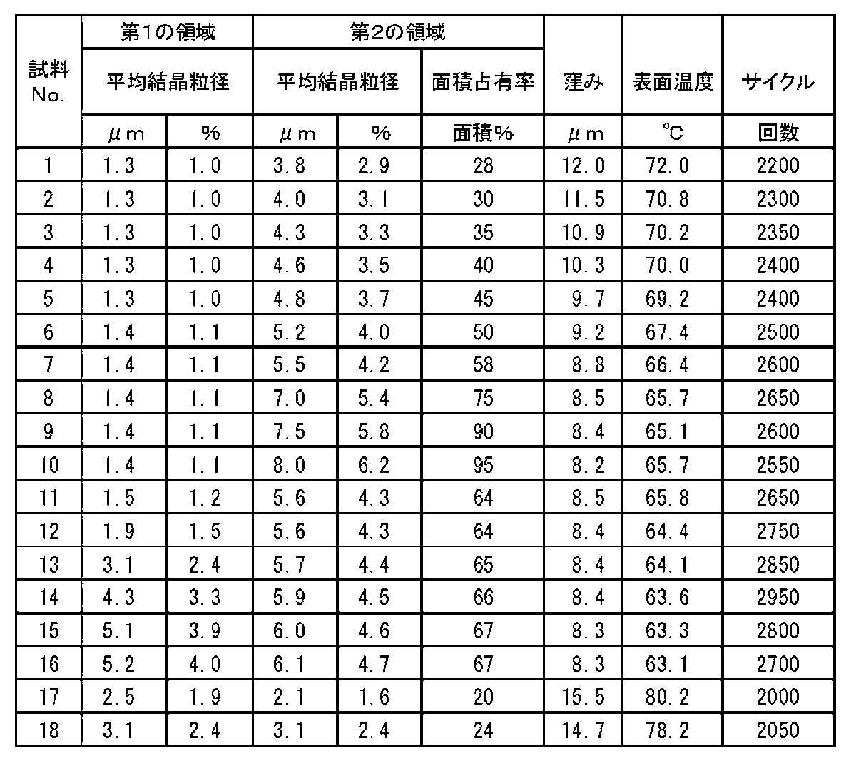
表1から、第1の領域13aにおける平均結晶粒径が、第2の領域13bにおける平均結晶粒径よりも大きい、または、第1の領域13aにおける平均結晶粒径と第2の領域13bにおける平均結晶粒径とが同じである試料No.17および18は、窪みが14.7μm以上、表面温度が78.2℃以上、サイクル数が2050以下であった。
これに対し、第2の領域13bにおける平均結晶粒径が、第1の領域13aにおける平均結晶粒径よりも大きい試料No.1~16は、窪みが12μm以下、表面温度が72℃以下、サイクル数が2200以上の結果が得られており、放熱特性および信頼性に優れた回路基板であることがわかった。
また、第2の領域13bに、貫通孔12の最小径の4%以上10%以下の結晶粒径の粒子が50面積%以上存在している試料No.6~16は、窪みが9.2μm以下、表面温度が67.4℃以下、サイクル数が2500以上の結果が得られており、より優れた回路基板であることがわかった。
さらに、第1の領域13aにおける平均結晶粒径が、貫通孔12の最小径の1.5%以上4%未満である試料No.12~15は、窪みが8.4μm以下、表面温度が64.4℃以下、サイクル数が2750以上の結果が得られており、さらに優れた回路基板であることがわかった。
次に、貫通導体13における第2の領域13bおよび金属配線層14の平均結晶粒径を異ならせた試料を作製し、放熱特性および信頼性に関する試験を行なった。製造方法としては、実施例1の試料No.14と同じ構成の貫通導体13上に、金属配線層14の平均結晶粒径を異ならせるべく、実施例1の試料No.4,8,14で第2の領域13bの形成に用いた金属ペーストを用いて金属配線層14を形成した。なお、金属配線層14の構成が実施例1の試料No.4の第2の領域13bと同じであるのが試料No.19であり、同様に試料No.14と同じであるのが試料No.20であり、試料No.8と同じであるのが試料No.21である。また、使用した金属ペーストを変更したこと以外は、実施例1と同様の方法で行なった。
そして、実施例1と同様の方法で、放熱特性試験およびヒートサイクル試験を行なった。結果を表2に示す。

表2から、試料No.19は、試料No.20,21よりもサイクル数が上回った結果が得られており、第2の領域13bにおける平均結晶粒径を、金属配線層14における平均結晶粒径よりも大きくすることによって、電子部品15の作動時に生じた熱の流れが、金属配線層14から貫通導体13の第2の領域13bへとスムーズに流れ、放熱特性の向上が図れることがわかった。
次に、第1の領域13aにおけるガラスの含有量と、第2の領域13bにおけるガラスの含有量を異ならせた試料を作製し、放熱特性および信頼性に関する試験を行なった。製造方法としては、第2の金属ペーストの配合比を変更し、試料No.22はガラス粉末を2.0質量%、試料No.23はガラス粉末を3.0質量%、試料No.24はガラス粉末を4.0質量%として変更した。なお、ガラス粉末を増減した量の分だけ、アクリル樹脂に対するテルピネオールの比率を3.4に固定しつつ、有機ビヒクルの添加量を増減した。また、使用した第2の金属ペーストを変更したこと以外は、実施例1と実施例2と同様の方法で行なった。
そして、実施例1と同様の方法で、放熱特性試験およびヒートサイクル試験を行なった。また、第1の領域13aおよび第2の領域13bにおけるガラスの含有量の測定方法は、まず、貫通導体13をセラミック焼結体11の厚み方向に切断し、クロスセクションポリッシャー(CP)を用いて研磨した面を測定面とした。次に、第1の領域13aおよび第2の領域13bについて、SEMに付設のEDSを用いて2000倍の倍率で確認し、任意の5点を選択して観察した。そして、各観察画像を画像解析ソフトを用いてガラスの含有量を求めて、それぞれ平均値を算出したものを第1の領域13aおよび第2の領域13bにおけるガラスの含有量とした。結果を表3に示す。

表3から、試料No.24は、試料No.22,23よりもサイクル数が上回った結果が得られており、第2の領域13bにおけるガラスの含有量を、第1の領域13aにおけるガラスの含有量よりも多くすることによって、貫通導体13の占有体積率の高い第2の領域13bの熱膨張を緩和することができるため、電子部品15の作動と停止を繰り返したときの冷熱サイクルの際の貫通導体13の形状変化を小さくすることができ、貫通孔12と貫通導体13との接合の剥がれを生じにくくできることがわかった。
次に、Biを含むガラスを添加した金属ペーストを用いて作製した試料(以下、Bi有り試料と)およびBiを含まないガラスを添加した金属ペーストを用いて作製した試料(以下、Bi無し試料)について、ヒートサイクル試験を行なった。なお、ガラス粉末として、R2O-SiO2-B2O3系またはR2O-SiO2-B2O3-Bi2O3系を用いたこと以外は、製造方法、試験方法ともに実施例1と同様の方法で行なった。なお、貫通孔12の内壁と貫通導体13との界面をTEMにて観察し、Biを含むガラスを添加した金属ペーストを用いて作製した試料については、Biの存在が確認された。
ヒートサイクル試験の結果、Bi無し試料に対し、Bi有り試料はサイクル数で10%の向上が見られ、Biを含むガラスを含有していることにより、貫通孔12の内壁と貫通導体13との接合強度を高めることができ、繰り返し掛かる熱によって貫通導体13が剥離することが少ない信頼性の高い回路基板とできることがわかった。
次に、セラミック焼結体11の両主面における貫通孔12の開口径を異ならせた試料を作製し、放熱特性および信頼性に関する試験を行なった。なお、製造方法としては、レーザー加工の発振出力の調整によって、表2に示すように、セラミック焼結体11の一方主面側および他方主面側の貫通孔12の径を異ならせたこと以外は実施例1と同様の方法で行なった。なお、貫通導体13および金属配線層14となる金属ペーストの構成は、実施例1の試料No.14と同じとした。
そして、実施例1と同様の方法で、放熱特性試験およびヒートサイクル試験を行なった。結果を表4に示す。
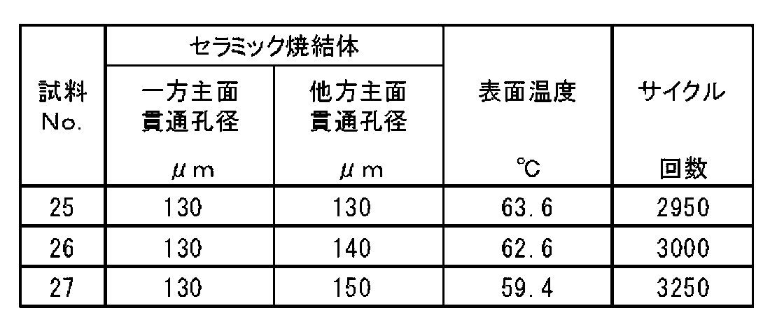
表2から、試料No.25に比べて試料No.26,27は、電子部品15が搭載されるセラミック焼結体11の一方主面に開口している貫通孔12の開口面積よりも、他方主面に開口している貫通孔12の開口面積が大きいので、放熱特性放熱性および信頼性がさらに優れた回路基板とできることがわかった。
1:電子装置
10:回路基板
11:セラミック焼結体
12:貫通孔
13:貫通導体
13a:第1の領域
13b:第2の領域
14:金属配線層
15:電子部品
16:電極パッド
10:回路基板
11:セラミック焼結体
12:貫通孔
13:貫通導体
13a:第1の領域
13b:第2の領域
14:金属配線層
15:電子部品
16:電極パッド
Claims (8)
- セラミック焼結体の厚み方向に貫通する貫通孔に金属からなる貫通導体を備えるとともに、前記セラミック焼結体の少なくとも一方主面側の前記貫通導体の表面を覆って接続されている金属配線層を備えた回路基板であって、前記貫通導体は、前記貫通孔の内壁側に前記セラミック焼結体の厚み方向に沿って前記貫通孔の一端から他端にかけて位置する第1の領域と、該第1の領域に隣接する第2の領域とを有し、該第2の領域における平均結晶粒径が、前記第1の領域における平均結晶粒径よりも大きいことを特徴とする回路基板。
- 前記第2の領域に、前記貫通孔の最小径の4%以上10%以下の結晶粒径の粒子が50面積%以上存在していることを特徴とする請求項1に記載の回路基板。
- 前記第1の領域における平均結晶粒径が、前記貫通孔の最小径の1.5%以上4%未満であることを特徴とする請求項1または請求項2に記載の回路基板。
- 前記第2の領域における平均結晶粒径が、前記金属配線層における平均結晶粒径よりも大きいことを特徴とする請求項1乃至請求項3のいずれかに記載の回路基板。
- 前記貫通導体がガラスを含有しており、前記第2の領域におけるガラスの含有量が、前記第1の領域におけるガラスの含有量より多いことを特徴とする請求項1乃至請求項4のいずれかに記載の回路基板。
- 前記貫通導体に含有されるガラスが、Biを含んでいることを特徴とする請求項1乃至請求項5のいずれかに記載の回路基板。
- 前記セラミック焼結体の一方主面に開口している前記貫通孔の開口面積よりも、他方主面に開口している前記貫通孔の開口面積が大きいことを特徴とする請求項1乃至請求項6のいずれかに記載の回路基板。
- 請求項1乃至請求項7のいずれかに記載の回路基板の前記金属配線層上に電子部品を搭載してなることを特徴とする電子装置。
Priority Applications (4)
| Application Number | Priority Date | Filing Date | Title |
|---|---|---|---|
| CN201280026481.2A CN103583087B (zh) | 2011-06-08 | 2012-05-30 | 电路基板以及具备该电路基板的电子装置 |
| EP12797274.3A EP2720520B1 (en) | 2011-06-08 | 2012-05-30 | Circuit board and electronic device provided with same |
| JP2013519455A JP5349714B2 (ja) | 2011-06-08 | 2012-05-30 | 回路基板およびこれを備える電子装置 |
| US14/124,227 US9820379B2 (en) | 2011-06-08 | 2012-05-30 | Circuit board and electronic device including same |
Applications Claiming Priority (2)
| Application Number | Priority Date | Filing Date | Title |
|---|---|---|---|
| JP2011128404 | 2011-06-08 | ||
| JP2011-128404 | 2011-06-08 |
Publications (1)
| Publication Number | Publication Date |
|---|---|
| WO2012169408A1 true WO2012169408A1 (ja) | 2012-12-13 |
Family
ID=47295974
Family Applications (1)
| Application Number | Title | Priority Date | Filing Date |
|---|---|---|---|
| PCT/JP2012/063946 Ceased WO2012169408A1 (ja) | 2011-06-08 | 2012-05-30 | 回路基板およびこれを備える電子装置 |
Country Status (5)
| Country | Link |
|---|---|
| US (1) | US9820379B2 (ja) |
| EP (1) | EP2720520B1 (ja) |
| JP (1) | JP5349714B2 (ja) |
| CN (1) | CN103583087B (ja) |
| WO (1) | WO2012169408A1 (ja) |
Cited By (10)
| Publication number | Priority date | Publication date | Assignee | Title |
|---|---|---|---|---|
| JP2015067492A (ja) * | 2013-09-30 | 2015-04-13 | 京セラ株式会社 | 金属層付きセラミック体、および金属層付きセラミック体の製造方法 |
| JP2015119165A (ja) * | 2013-11-12 | 2015-06-25 | セイコーエプソン株式会社 | 配線基板の製造方法、配線基板、素子収納用パッケージ、電子デバイス、電子機器および移動体 |
| JP2015224151A (ja) * | 2014-05-27 | 2015-12-14 | Ngkエレクトロデバイス株式会社 | Cu/セラミック基板 |
| JP2017139345A (ja) * | 2016-02-04 | 2017-08-10 | 株式会社日立製作所 | 半導体装置、並びに半導体装置の製造方法 |
| JP2019073437A (ja) * | 2018-12-11 | 2019-05-16 | Ngkエレクトロデバイス株式会社 | Cu/セラミック基板 |
| JP2019110223A (ja) * | 2017-12-19 | 2019-07-04 | 三菱マテリアル株式会社 | パワーモジュール用基板及びその製造方法 |
| JP2019165155A (ja) * | 2018-03-20 | 2019-09-26 | 東洋アルミニウム株式会社 | 窒化アルミニウム回路基板及びその製造方法 |
| JP2019220525A (ja) * | 2018-06-18 | 2019-12-26 | 大日本印刷株式会社 | 配線基板および配線基板の製造方法 |
| CN110800118A (zh) * | 2017-06-29 | 2020-02-14 | 京瓷株式会社 | 电路基板以及具备该电路基板的发光装置 |
| WO2025143007A1 (ja) * | 2023-12-27 | 2025-07-03 | 京セラ株式会社 | 多層基板 |
Families Citing this family (11)
| Publication number | Priority date | Publication date | Assignee | Title |
|---|---|---|---|---|
| WO2016119807A1 (de) * | 2015-01-28 | 2016-08-04 | Sew-Eurodrive Gmbh & Co. Kg | Elektrogerät |
| US9706639B2 (en) * | 2015-06-18 | 2017-07-11 | Samsung Electro-Mechanics Co., Ltd. | Circuit board and method of manufacturing the same |
| DE112017002999B4 (de) * | 2016-06-16 | 2022-03-24 | Mitsubishi Electric Corporation | Halbleiter-montage-wärmeabführungs-basisplatte und herstellungsverfahren für dieselbe |
| JP6970738B2 (ja) * | 2017-03-30 | 2021-11-24 | 株式会社東芝 | セラミックス銅回路基板およびそれを用いた半導体装置 |
| CN111052879B (zh) * | 2017-08-29 | 2023-03-31 | 京瓷株式会社 | 电路基板及具备该电路基板的电子装置 |
| JP7124633B2 (ja) * | 2017-10-27 | 2022-08-24 | 三菱マテリアル株式会社 | 接合体、及び、絶縁回路基板 |
| JP6605164B1 (ja) * | 2018-12-27 | 2019-11-13 | 日本碍子株式会社 | 燃料電池のセルスタック |
| JP7332128B2 (ja) * | 2019-01-10 | 2023-08-23 | 株式会社マテリアル・コンセプト | 電子部品及びその製造方法 |
| CN112117204B (zh) * | 2020-09-10 | 2022-10-14 | 安徽龙芯微科技有限公司 | 一种封装结构的制作方法 |
| CN115966472B (zh) * | 2022-12-21 | 2025-12-23 | 福建闽航电子有限公司 | 一种陶瓷外壳封装体的制造方法及陶瓷外壳封装体 |
| CN119785673B (zh) * | 2025-02-19 | 2025-12-05 | 深圳市艾比森光电股份有限公司 | Led显示屏、led显示模组及其制备方法 |
Citations (6)
| Publication number | Priority date | Publication date | Assignee | Title |
|---|---|---|---|---|
| JPH0946013A (ja) | 1995-05-19 | 1997-02-14 | Nikko Co | スルーホール充填用導体ペースト及びセラミック回路基板 |
| JPH11251700A (ja) * | 1998-02-26 | 1999-09-17 | Kyocera Corp | 銅メタライズ組成物及びそれを用いたガラスセラミック配線基板 |
| JP2003110241A (ja) * | 2001-09-28 | 2003-04-11 | Kyocera Corp | 配線基板およびこれを用いた電子装置 |
| JP2004134467A (ja) * | 2002-10-08 | 2004-04-30 | Fujikura Ltd | 多層配線基板、多層配線基板用基材およびその製造方法 |
| WO2005027606A1 (ja) * | 2003-09-09 | 2005-03-24 | Hoya Corporation | 両面配線ガラス基板の製造方法 |
| JP2009054773A (ja) * | 2007-08-27 | 2009-03-12 | Fujikura Ltd | 多層配線板及びその製造方法 |
Family Cites Families (13)
| Publication number | Priority date | Publication date | Assignee | Title |
|---|---|---|---|---|
| JPH05259529A (ja) * | 1992-03-11 | 1993-10-08 | Sankyo Seiki Mfg Co Ltd | 絶縁基板及びその製造方法 |
| JP3785032B2 (ja) * | 2000-08-22 | 2006-06-14 | 日本特殊陶業株式会社 | プリント配線基板におけるスルーホール構造及びその製造方法 |
| JP4576728B2 (ja) * | 2001-03-06 | 2010-11-10 | ソニー株式会社 | 導電性ぺースト、プリント配線基板とその製造方法および半導体装置とその製造方法 |
| JP2004055593A (ja) * | 2002-07-16 | 2004-02-19 | Hoya Corp | 配線基板およびその製造方法 |
| JP2004140005A (ja) * | 2002-08-23 | 2004-05-13 | Kyocera Corp | 配線基板 |
| US7233073B2 (en) * | 2003-07-31 | 2007-06-19 | Matsushita Electric Industrial Co., Ltd. | Semiconductor device and method for fabricating the same |
| JP2007273648A (ja) * | 2006-03-30 | 2007-10-18 | Furukawa Electric Co Ltd:The | プリント配線板及びその製造方法 |
| US20100103634A1 (en) * | 2007-03-30 | 2010-04-29 | Takuo Funaya | Functional-device-embedded circuit board, method for manufacturing the same, and electronic equipment |
| US7741226B2 (en) * | 2008-05-06 | 2010-06-22 | International Business Machines Corporation | Optimal tungsten through wafer via and process of fabricating same |
| CN101752299B (zh) | 2008-12-09 | 2012-05-16 | 中芯国际集成电路制造(上海)有限公司 | 插塞结构的制作方法和插塞结构 |
| EP2483941B1 (en) * | 2009-09-30 | 2015-03-25 | Canon Kabushiki Kaisha | Piezolectric material comprising tungsten bronze structure metal oxide |
| US8617982B2 (en) * | 2010-10-05 | 2013-12-31 | Novellus Systems, Inc. | Subtractive patterning to define circuit components |
| JP5857032B2 (ja) * | 2011-03-02 | 2016-02-10 | 日立オートモティブシステムズ株式会社 | 熱式流量計 |
-
2012
- 2012-05-30 WO PCT/JP2012/063946 patent/WO2012169408A1/ja not_active Ceased
- 2012-05-30 CN CN201280026481.2A patent/CN103583087B/zh not_active Expired - Fee Related
- 2012-05-30 US US14/124,227 patent/US9820379B2/en not_active Expired - Fee Related
- 2012-05-30 EP EP12797274.3A patent/EP2720520B1/en not_active Not-in-force
- 2012-05-30 JP JP2013519455A patent/JP5349714B2/ja not_active Expired - Fee Related
Patent Citations (6)
| Publication number | Priority date | Publication date | Assignee | Title |
|---|---|---|---|---|
| JPH0946013A (ja) | 1995-05-19 | 1997-02-14 | Nikko Co | スルーホール充填用導体ペースト及びセラミック回路基板 |
| JPH11251700A (ja) * | 1998-02-26 | 1999-09-17 | Kyocera Corp | 銅メタライズ組成物及びそれを用いたガラスセラミック配線基板 |
| JP2003110241A (ja) * | 2001-09-28 | 2003-04-11 | Kyocera Corp | 配線基板およびこれを用いた電子装置 |
| JP2004134467A (ja) * | 2002-10-08 | 2004-04-30 | Fujikura Ltd | 多層配線基板、多層配線基板用基材およびその製造方法 |
| WO2005027606A1 (ja) * | 2003-09-09 | 2005-03-24 | Hoya Corporation | 両面配線ガラス基板の製造方法 |
| JP2009054773A (ja) * | 2007-08-27 | 2009-03-12 | Fujikura Ltd | 多層配線板及びその製造方法 |
Cited By (13)
| Publication number | Priority date | Publication date | Assignee | Title |
|---|---|---|---|---|
| JP2015067492A (ja) * | 2013-09-30 | 2015-04-13 | 京セラ株式会社 | 金属層付きセラミック体、および金属層付きセラミック体の製造方法 |
| JP2015119165A (ja) * | 2013-11-12 | 2015-06-25 | セイコーエプソン株式会社 | 配線基板の製造方法、配線基板、素子収納用パッケージ、電子デバイス、電子機器および移動体 |
| JP2015224151A (ja) * | 2014-05-27 | 2015-12-14 | Ngkエレクトロデバイス株式会社 | Cu/セラミック基板 |
| JP2017139345A (ja) * | 2016-02-04 | 2017-08-10 | 株式会社日立製作所 | 半導体装置、並びに半導体装置の製造方法 |
| CN110800118A (zh) * | 2017-06-29 | 2020-02-14 | 京瓷株式会社 | 电路基板以及具备该电路基板的发光装置 |
| CN110800118B (zh) * | 2017-06-29 | 2022-10-28 | 京瓷株式会社 | 电路基板以及具备该电路基板的发光装置 |
| JP7008236B2 (ja) | 2017-12-19 | 2022-01-25 | 三菱マテリアル株式会社 | パワーモジュール用基板及びその製造方法 |
| JP2019110223A (ja) * | 2017-12-19 | 2019-07-04 | 三菱マテリアル株式会社 | パワーモジュール用基板及びその製造方法 |
| JP2019165155A (ja) * | 2018-03-20 | 2019-09-26 | 東洋アルミニウム株式会社 | 窒化アルミニウム回路基板及びその製造方法 |
| JP2019220525A (ja) * | 2018-06-18 | 2019-12-26 | 大日本印刷株式会社 | 配線基板および配線基板の製造方法 |
| JP7119620B2 (ja) | 2018-06-18 | 2022-08-17 | 大日本印刷株式会社 | 配線基板および配線基板の製造方法 |
| JP2019073437A (ja) * | 2018-12-11 | 2019-05-16 | Ngkエレクトロデバイス株式会社 | Cu/セラミック基板 |
| WO2025143007A1 (ja) * | 2023-12-27 | 2025-07-03 | 京セラ株式会社 | 多層基板 |
Also Published As
| Publication number | Publication date |
|---|---|
| EP2720520A4 (en) | 2015-05-27 |
| JPWO2012169408A1 (ja) | 2015-02-23 |
| JP5349714B2 (ja) | 2013-11-20 |
| EP2720520B1 (en) | 2019-01-02 |
| US20140268589A1 (en) | 2014-09-18 |
| US9820379B2 (en) | 2017-11-14 |
| EP2720520A1 (en) | 2014-04-16 |
| CN103583087A (zh) | 2014-02-12 |
| CN103583087B (zh) | 2017-05-24 |
Similar Documents
| Publication | Publication Date | Title |
|---|---|---|
| JP5349714B2 (ja) | 回路基板およびこれを備える電子装置 | |
| JP5677585B2 (ja) | 回路基板およびこれを備える電子装置 | |
| JP5905962B2 (ja) | 回路基板およびこれを備える電子装置 | |
| JP5806030B2 (ja) | 回路基板およびこれを備える電子装置 | |
| CN107535048B (zh) | 电路基板以及具备该电路基板的电子装置 | |
| JP6114001B2 (ja) | 導電性ペーストおよび回路基板ならびに電子装置 | |
| JP6298174B2 (ja) | 回路基板およびこれを備える電子装置 | |
| JP6430886B2 (ja) | 回路基板およびこれを備える電子装置 | |
| JP5840945B2 (ja) | 回路基板およびこれを備える電子装置 | |
| JP5743916B2 (ja) | 回路基板およびこれを備える電子装置 | |
| JP2013051253A (ja) | 回路基板およびこれを備える電子装置 | |
| JP6608562B2 (ja) | 回路基板およびこれを備える電子装置 | |
| JP2014168053A (ja) | 回路基板およびこれを備える電子装置 | |
| JP2002128581A (ja) | 銅メタライズ組成物ならびにそれを用いたセラミック配線基板およびその製造方法 | |
| TW202231398A (zh) | 氧化銅糊料及電子零件之製造方法 | |
| JP2018170506A (ja) | 回路基板およびこれを備える電子装置 | |
| JP2006080363A (ja) | 導電性ペースト | |
| JP2011154807A (ja) | 銅メタライズ組成物およびそれを用いたガラスセラミック配線基板 |
Legal Events
| Date | Code | Title | Description |
|---|---|---|---|
| 121 | Ep: the epo has been informed by wipo that ep was designated in this application |
Ref document number: 12797274 Country of ref document: EP Kind code of ref document: A1 |
|
| ENP | Entry into the national phase |
Ref document number: 2013519455 Country of ref document: JP Kind code of ref document: A |
|
| NENP | Non-entry into the national phase |
Ref country code: DE |
|
| WWE | Wipo information: entry into national phase |
Ref document number: 14124227 Country of ref document: US |