WO2012169408A1 - Circuit imprimé et dispositif électrique équipé de celui-ci - Google Patents
Circuit imprimé et dispositif électrique équipé de celui-ci Download PDFInfo
- Publication number
- WO2012169408A1 WO2012169408A1 PCT/JP2012/063946 JP2012063946W WO2012169408A1 WO 2012169408 A1 WO2012169408 A1 WO 2012169408A1 JP 2012063946 W JP2012063946 W JP 2012063946W WO 2012169408 A1 WO2012169408 A1 WO 2012169408A1
- Authority
- WO
- WIPO (PCT)
- Prior art keywords
- region
- conductor
- hole
- circuit board
- crystal grain
- Prior art date
- Legal status (The legal status is an assumption and is not a legal conclusion. Google has not performed a legal analysis and makes no representation as to the accuracy of the status listed.)
- Ceased
Links
Images


Classifications
-
- H—ELECTRICITY
- H05—ELECTRIC TECHNIQUES NOT OTHERWISE PROVIDED FOR
- H05K—PRINTED CIRCUITS; CASINGS OR CONSTRUCTIONAL DETAILS OF ELECTRIC APPARATUS; MANUFACTURE OF ASSEMBLAGES OF ELECTRICAL COMPONENTS
- H05K1/00—Printed circuits
- H05K1/02—Details
- H05K1/09—Use of materials for the conductive, e.g. metallic pattern
-
- H—ELECTRICITY
- H05—ELECTRIC TECHNIQUES NOT OTHERWISE PROVIDED FOR
- H05K—PRINTED CIRCUITS; CASINGS OR CONSTRUCTIONAL DETAILS OF ELECTRIC APPARATUS; MANUFACTURE OF ASSEMBLAGES OF ELECTRICAL COMPONENTS
- H05K1/00—Printed circuits
- H05K1/02—Details
- H05K1/0201—Thermal arrangements, e.g. for cooling, heating or preventing overheating
- H05K1/0203—Cooling of mounted components
- H05K1/0204—Cooling of mounted components using means for thermal conduction connection in the thickness direction of the substrate
- H05K1/0206—Cooling of mounted components using means for thermal conduction connection in the thickness direction of the substrate by printed thermal vias
-
- H—ELECTRICITY
- H05—ELECTRIC TECHNIQUES NOT OTHERWISE PROVIDED FOR
- H05K—PRINTED CIRCUITS; CASINGS OR CONSTRUCTIONAL DETAILS OF ELECTRIC APPARATUS; MANUFACTURE OF ASSEMBLAGES OF ELECTRICAL COMPONENTS
- H05K1/00—Printed circuits
- H05K1/02—Details
- H05K1/03—Use of materials for the substrate
- H05K1/0306—Inorganic insulating substrates, e.g. ceramic, glass
-
- H—ELECTRICITY
- H05—ELECTRIC TECHNIQUES NOT OTHERWISE PROVIDED FOR
- H05K—PRINTED CIRCUITS; CASINGS OR CONSTRUCTIONAL DETAILS OF ELECTRIC APPARATUS; MANUFACTURE OF ASSEMBLAGES OF ELECTRICAL COMPONENTS
- H05K1/00—Printed circuits
- H05K1/02—Details
- H05K1/11—Printed elements for providing electric connections to or between printed circuits
- H05K1/115—Via connections; Lands around holes or via connections
-
- H—ELECTRICITY
- H10—SEMICONDUCTOR DEVICES; ELECTRIC SOLID-STATE DEVICES NOT OTHERWISE PROVIDED FOR
- H10W—GENERIC PACKAGES, INTERCONNECTIONS, CONNECTORS OR OTHER CONSTRUCTIONAL DETAILS OF DEVICES COVERED BY CLASS H10
- H10W40/00—Arrangements for thermal protection or thermal control
- H10W40/20—Arrangements for cooling
- H10W40/22—Arrangements for cooling characterised by their shape, e.g. having conical or cylindrical projections
- H10W40/226—Arrangements for cooling characterised by their shape, e.g. having conical or cylindrical projections characterised by projecting parts, e.g. fins to increase surface area
- H10W40/228—Arrangements for cooling characterised by their shape, e.g. having conical or cylindrical projections characterised by projecting parts, e.g. fins to increase surface area the projecting parts being wire-shaped or pin-shaped
-
- H—ELECTRICITY
- H10—SEMICONDUCTOR DEVICES; ELECTRIC SOLID-STATE DEVICES NOT OTHERWISE PROVIDED FOR
- H10W—GENERIC PACKAGES, INTERCONNECTIONS, CONNECTORS OR OTHER CONSTRUCTIONAL DETAILS OF DEVICES COVERED BY CLASS H10
- H10W70/00—Package substrates; Interposers; Redistribution layers [RDL]
- H10W70/60—Insulating or insulated package substrates; Interposers; Redistribution layers
- H10W70/62—Insulating or insulated package substrates; Interposers; Redistribution layers characterised by their interconnections
- H10W70/63—Vias, e.g. via plugs
- H10W70/635—Through-vias
-
- H—ELECTRICITY
- H10—SEMICONDUCTOR DEVICES; ELECTRIC SOLID-STATE DEVICES NOT OTHERWISE PROVIDED FOR
- H10W—GENERIC PACKAGES, INTERCONNECTIONS, CONNECTORS OR OTHER CONSTRUCTIONAL DETAILS OF DEVICES COVERED BY CLASS H10
- H10W70/00—Package substrates; Interposers; Redistribution layers [RDL]
- H10W70/60—Insulating or insulated package substrates; Interposers; Redistribution layers
- H10W70/67—Insulating or insulated package substrates; Interposers; Redistribution layers characterised by their insulating layers or insulating parts
- H10W70/69—Insulating materials thereof
- H10W70/692—Ceramics or glasses
-
- H—ELECTRICITY
- H05—ELECTRIC TECHNIQUES NOT OTHERWISE PROVIDED FOR
- H05K—PRINTED CIRCUITS; CASINGS OR CONSTRUCTIONAL DETAILS OF ELECTRIC APPARATUS; MANUFACTURE OF ASSEMBLAGES OF ELECTRICAL COMPONENTS
- H05K2201/00—Indexing scheme relating to printed circuits covered by H05K1/00
- H05K2201/02—Fillers; Particles; Fibers; Reinforcement materials
- H05K2201/0203—Fillers and particles
- H05K2201/0263—Details about a collection of particles
- H05K2201/0266—Size distribution
-
- H—ELECTRICITY
- H05—ELECTRIC TECHNIQUES NOT OTHERWISE PROVIDED FOR
- H05K—PRINTED CIRCUITS; CASINGS OR CONSTRUCTIONAL DETAILS OF ELECTRIC APPARATUS; MANUFACTURE OF ASSEMBLAGES OF ELECTRICAL COMPONENTS
- H05K2201/00—Indexing scheme relating to printed circuits covered by H05K1/00
- H05K2201/03—Conductive materials
- H05K2201/032—Materials
- H05K2201/0326—Inorganic, non-metallic conductor, e.g. indium-tin oxide [ITO]
-
- H—ELECTRICITY
- H05—ELECTRIC TECHNIQUES NOT OTHERWISE PROVIDED FOR
- H05K—PRINTED CIRCUITS; CASINGS OR CONSTRUCTIONAL DETAILS OF ELECTRIC APPARATUS; MANUFACTURE OF ASSEMBLAGES OF ELECTRICAL COMPONENTS
- H05K2203/00—Indexing scheme relating to apparatus or processes for manufacturing printed circuits covered by H05K3/00
- H05K2203/04—Soldering or other types of metallurgic bonding
- H05K2203/049—Wire bonding
-
- H—ELECTRICITY
- H05—ELECTRIC TECHNIQUES NOT OTHERWISE PROVIDED FOR
- H05K—PRINTED CIRCUITS; CASINGS OR CONSTRUCTIONAL DETAILS OF ELECTRIC APPARATUS; MANUFACTURE OF ASSEMBLAGES OF ELECTRICAL COMPONENTS
- H05K3/00—Apparatus or processes for manufacturing printed circuits
- H05K3/40—Forming printed elements for providing electric connections to or between printed circuits
- H05K3/4038—Through-connections; Vertical interconnect access [VIA] connections
- H05K3/4053—Through-connections; Vertical interconnect access [VIA] connections by thick-film techniques
- H05K3/4061—Through-connections; Vertical interconnect access [VIA] connections by thick-film techniques for via connections in inorganic insulating substrates
-
- H—ELECTRICITY
- H10—SEMICONDUCTOR DEVICES; ELECTRIC SOLID-STATE DEVICES NOT OTHERWISE PROVIDED FOR
- H10W—GENERIC PACKAGES, INTERCONNECTIONS, CONNECTORS OR OTHER CONSTRUCTIONAL DETAILS OF DEVICES COVERED BY CLASS H10
- H10W72/00—Interconnections or connectors in packages
- H10W72/851—Dispositions of multiple connectors or interconnections
- H10W72/874—On different surfaces
- H10W72/884—Die-attach connectors and bond wires
-
- H—ELECTRICITY
- H10—SEMICONDUCTOR DEVICES; ELECTRIC SOLID-STATE DEVICES NOT OTHERWISE PROVIDED FOR
- H10W—GENERIC PACKAGES, INTERCONNECTIONS, CONNECTORS OR OTHER CONSTRUCTIONAL DETAILS OF DEVICES COVERED BY CLASS H10
- H10W90/00—Package configurations
- H10W90/701—Package configurations characterised by the relative positions of pads or connectors relative to package parts
- H10W90/731—Package configurations characterised by the relative positions of pads or connectors relative to package parts of die-attach connectors
- H10W90/734—Package configurations characterised by the relative positions of pads or connectors relative to package parts of die-attach connectors between a chip and a stacked insulating package substrate, interposer or RDL
-
- H—ELECTRICITY
- H10—SEMICONDUCTOR DEVICES; ELECTRIC SOLID-STATE DEVICES NOT OTHERWISE PROVIDED FOR
- H10W—GENERIC PACKAGES, INTERCONNECTIONS, CONNECTORS OR OTHER CONSTRUCTIONAL DETAILS OF DEVICES COVERED BY CLASS H10
- H10W90/00—Package configurations
- H10W90/701—Package configurations characterised by the relative positions of pads or connectors relative to package parts
- H10W90/751—Package configurations characterised by the relative positions of pads or connectors relative to package parts of bond wires
- H10W90/754—Package configurations characterised by the relative positions of pads or connectors relative to package parts of bond wires between a chip and a stacked insulating package substrate, interposer or RDL
Definitions
- the present invention relates to a circuit board and an electronic device in which electronic components are mounted on the circuit board.
- An electronic device in which various electronic parts such as a semiconductor element, a heating element, and a Peltier element are mounted via a metal wiring layer bonded on a circuit board is used. These electronic components generate heat during operation, and the amount of heat applied per volume of the circuit board is increasing due to the recent high integration of electronic components and the miniaturization and thinning of electronic devices. In addition to the fact that bonding is not peeled off, a circuit board having high heat dissipation characteristics is required.
- a through hole is formed in a portion immediately below the electronic component, and the heat radiation characteristics are improved by using a conductor (hereinafter referred to as a through conductor) provided in the through hole.
- a conductor hereinafter referred to as a through conductor
- the metal plating grows from the inner wall of the through hole, so that a depression is generated at the center of the surface of the through conductor.
- the metal paste is filled, a depression is generated in the center of the surface of the through conductor due to shrinkage during firing.
- the metal wiring layer formed to cover the surface of the through conductor has a surface property that follows the surface property of the through conductor.
- Patent Document 1 discloses a conductive paste for filling a through hole formed in a ceramic substrate and then firing the conductive paste, the conductive powder having a metal powder as a main component. And a non-shrinkable through-hole filling conductor paste containing a swelling agent and a color developing agent.
- the present invention provides a highly reliable circuit board that can be used for a long period of time by reducing the dent of the metal wiring layer formed on the through conductor while having high bonding strength and excellent heat dissipation characteristics, and this circuit An electronic device in which electronic components are mounted on a substrate is provided.
- the circuit board of the present invention includes a through conductor made of metal in a through hole penetrating in the thickness direction of the ceramic sintered body, and covers and connects the surface of the through conductor on at least one main surface side of the ceramic sintered body.
- the through-conductor is provided on the inner wall side of the through-hole along the thickness direction of the ceramic sintered body from one end to the other end of the through-hole. 1 region and a second region adjacent to the first region, wherein the average crystal grain size in the second region is larger than the average crystal grain size in the first region It is what.
- the electronic device of the present invention is characterized in that an electronic component is mounted on the metal wiring layer of the circuit board of the present invention having the above-described configuration.
- the shrinkage of the metal paste during firing on the center side of the diameter of the through hole is small.
- the depression of the through conductor can be reduced.
- the second region having a large average crystal grain size on the center side of the diameter of the through hole heat generated during operation of the electronic component transmitted to one end side of the through hole can be quickly transferred to the other end side. Therefore, the heat dissipation characteristics can be improved.
- the first region having a small average crystal grain size is located from one end of the through hole to the other end along the thickness direction of the ceramic sintered body on the inner wall side of the through hole, the bonding strength of the through conductor is increased. Can be expensive.
- the electronic device of the present invention it is possible to obtain a highly reliable electronic device by mounting electronic components on the metal wiring layer of the circuit board of the present invention.
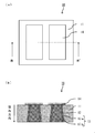
- FIG. 1A is an excerpt of a circuit board in the electronic device shown in FIG. 1
- FIG. 1B is a cross-sectional view taken along line A-A ′ in FIG.
- the other example of the circuit board of this embodiment is shown, (a) is a plan view, (b) is a cross-sectional view taken along line B-B 'of (a).
- FIG. 1 is a cross-sectional view showing an example of an electronic device including the circuit board of the present embodiment.
- the electronic device 1 of the present embodiment includes a through conductor 13 made of metal in the thickness direction of the ceramic sintered body 11 (the through hole 12 penetrating in the drawing and the through conductor 13 on the one main surface side of the ceramic sintered body 11.
- the circuit board 10 is provided with a metal wiring layer 14 connected so as to cover the surface of the substrate 10. On the metal wiring layer 14 constituting the circuit board 10, for example, electrode pads 16 are provided.
- the electronic component 15 is mounted on the electrode pad 16 and is electrically joined by the bonding wire 17 to obtain the electronic device 1 of the present embodiment.
- examples of the electronic component 15 include an insulated gate bipolar transistor (IGBT) element, an intelligent power module (IPM) element, a metal oxide film field effect transistor (MOSFET) element, and a light emitting diode (LED) element.
- IGBT insulated gate bipolar transistor
- IPM intelligent power module
- MOSFET metal oxide film field effect transistor
- LED light emitting diode
- Semiconductor elements such as freewheeling diode (FWD) element, giant transistor (GTR) element, Schottky barrier diode (SBD), heating element for sublimation type thermal printer head or thermal inkjet printer head, Peltier element, etc. Can be used.
- FIG. 2A and 2B show an excerpt of the circuit board 10 in the electronic device shown in FIG. 1, wherein FIG. 2A is a plan view and FIG. 2B is a cross-sectional view taken along line A-A ′ of FIG.
- FIG. 2A is a plan view
- FIG. 2B is a cross-sectional view taken along line A-A ′ of FIG.
- the circuit board 10 of the present embodiment includes a through conductor 13 made of metal in a through hole 12 that penetrates in the thickness direction of the ceramic sintered body 11, and includes at least the ceramic sintered body 11.
- a metal wiring layer 14 is provided so as to cover the surface of the through conductor 13 on the main surface side, and the through conductor 13 is formed on the inner wall side of the through hole 12 along the thickness direction of the ceramic sintered body 11. Having a first region 13a located from one end to the other end and a second region 13b adjacent to the first region 13a, the average crystal grain size in the second region 13b being the first region 13a. It is characterized by being larger than the average crystal grain size.
- the diameter of the through hole 12 is increased. Since the metal paste having a large crystal grain size is present on the center side of the through hole 12, the shrinkage of the metal paste during firing on the center side of the diameter of the through hole 12 is small, so that the depression of the through conductor 13 can be reduced. it can.
- the depression of the metal wiring layer 14 connected to cover the surface of the through conductor 13 can be reduced, and when an electronic component (not shown) is mounted on the metal wiring layer 14 via the electrode pad, It is possible to reduce the occurrence of problems such as the contact area being reduced and the heat dissipation characteristics being lowered, or the electrode pad being detached and not functioning as an electronic device. Further, since the second region 13b having a large average crystal grain size is provided on the center side of the diameter of the through hole 12, it is generated when an electronic component (not shown) transmitted to one end side of the through hole 12 is operated. Heat can be transferred to the other end side quickly, so that the heat dissipation characteristics can be improved.
- the first region 13a having a small average crystal grain size is provided on the inner wall side of the through hole 12, whereby the through conductor 13 in the through hole 12 is provided.
- the bonding strength of can be made high.
- the first region 13a and the second region 13b are, for example, the center of the diameter of the through hole 12 in the cross-sectional view shown in FIG. From the center to the inner wall of the through-hole 12, the portion corresponding to 4/5 of the radius from the center is the second region 13b, and the portion corresponding to the inner wall side other than the second region 13b is the first region 13a.
- the diameter (diameter) of the through hole 12 is 130 ⁇ m (65 ⁇ m in radius)
- a portion corresponding to a circle having a radius of 52 ⁇ m from the center of the diameter of the through hole 12 toward the inner wall is the second region 13b.
- the portion corresponding to the inner wall side other than the second region 13b is the first region 13a.
- the through conductor 13 is cut in the thickness direction of the ceramic sintered body 11, and the ceramic firing is performed using a cross section polisher (CP). What is necessary is just to confirm the surface grind
- any five points of the first region 13a and the second region 13b are selected.
- the crystal grain size may be obtained for each observation image using image analysis software, and the average crystal grain size may be calculated from the value of each crystal grain size.
- the depression of the metal wiring layer 14 connected to cover the surface of the through conductor 13 can be measured by using a surface roughness meter or a laser displacement meter.
- a surface roughness meter or a laser displacement meter For example, when measuring with a laser displacement meter, the surface of the metal wiring layer 14 located where the surface of the through conductor 13 is not covered and the metal wiring layer 14 located where the surface of the through conductor 13 is covered It is only necessary to measure several points on the surface and set the difference between the maximum value and the minimum value of the measured value as the value of the depression.
- the circuit board 10 of the present embodiment it is preferable that particles having a crystal grain size of 4% or more and 10% or less of the minimum diameter of the through hole 12 are present in the second region 13b by 50 area% or more.
- particles having a crystal grain size of 4% or more and 10% or less of the minimum diameter of the through hole 12 are present in the second region 13b by 50 area% or more.
- the dent can be reduced and the through hole can be reduced. Heat generated during operation of the electronic component transmitted to one end side of 12 can be transferred to the other end side more quickly, and heat dissipation characteristics can be improved.
- the area occupancy of the particles having a crystal grain size of 4% or more and 10% or less of the minimum diameter of the through-hole 12 is, for example, the same as in the calculation of the average crystal grain size. What is necessary is just to calculate the area occupation rate of the crystal grain diameter of 4% or more and 10% or less of the minimum diameter of the through hole 12 in the second region 13b by using image analysis software.
- the average crystal grain size in the second region 13b is preferably 3.1% to 5.8% of the minimum diameter of the through hole 12.
- the through conductor constituting the circuit board 10 of the present embodiment in the 13th second region 13b, voids having an average diameter of 1% or more and 4% or less of the minimum diameter of the through hole 12 are present in a range of 3% by area or more and 5% by area or less.
- the voids present in the second region 13b contribute to reducing the depression of the through conductor 13 without reducing the thermal conductivity.
- the binarization process is performed on the observed image using image analysis software, as in the calculation of the average crystal grain size.
- the voids may be extracted by calculating the average void diameter and void ratio.
- the average crystal grain size in the first region 13a is preferably 1.5% or more and less than 4% of the minimum diameter of the through hole 12.
- the bonding strength of the through conductor 13 in the through hole 12 can be increased, Also in the first region 13b, heat generated during operation of the electronic component transmitted to one end side of the through hole 12 can be quickly transferred to the other end side.
- the average crystal grain size in the second region 13b is larger than the average crystal grain size in the metal wiring layer 14.
- the heat flow generated during the operation of the electronic component 15 causes the second flow of the through conductor 13 from the metal wiring layer 14. Therefore, the heat dissipation characteristics can be improved.
- the metal wiring layer 14 is cut in the thickness direction of the ceramic sintered body 11, and polished by using a cross section polisher (CP). Next, confirm using SEM at a magnification of 5000 times, select and observe any five points, determine the crystal grain size using image analysis software for each observation image, and average from the value of each crystal grain size What is necessary is just to calculate a crystal grain size.
- the through conductor 13 contains glass, and the glass content in the second region 13b is larger than the glass content in the first region 13a.
- the thermal expansion of the second region 13b having a high occupied volume ratio of the through conductor 13 can be reduced. Therefore, the shape change of the through conductor 13 during the cooling cycle when the electronic component 15 is repeatedly activated and stopped is reduced, and it is possible to make it difficult for the through hole 12 and the through conductor 13 to be peeled off.
- the glass content in the first region 13a and the second region 13b is measured by, for example, cutting the through conductor 13 in the thickness direction of the ceramic sintered body 11 and using a cross section polisher (CP).
- the polished surface is taken as the measurement surface.
- the boundary between the first region 13a and the second region 13b is confirmed by the method described above, and each of the first region 13a and the second region 13b is subjected to EDS (energy dispersive X-type) attached to the SEM.
- EDS energy dispersive X-type
- the through conductor 13 contains glass containing Bi.
- the through conductor 13 contains Bi-containing glass, the wettability with the ceramic sintered body 11 is good, so that the bonding strength of the through conductor 13 in the through hole 12 can be made higher. This is based on the fact that a large amount of Bi is present at the interface with the inner wall of the through hole 12 when the bonding strength of the through conductor 13 in the through hole 12 is high.
- the glass containing Bi include SiO 2 —B 2 O 3 —Bi 2 O 3 glass and R 2 O—SiO 2 —B 2 O 3 —Bi 2 O 3 glass (R: alkali metal).
- the Bi may be confirmed using, for example, a TEM (transmission electron microscope) or an EDS attached to the SEM.
- the thickness of the glass is, for example, not less than 0.5 ⁇ m and not more than 5.0 ⁇ m.
- FIG. 3A and 3B show another example of the circuit board of the present embodiment, in which FIG. 3A is a plan view and FIG. 3B is a cross-sectional view taken along line B-B ′ in FIG.
- the circuit board 10 in FIG. 3 is open on the other main surface rather than the opening area of the through hole 12 opened on one main surface (surface on which electronic components are mounted) of the ceramic sintered body 11.
- the opening area of the through hole 12 is large, an example in which the diameter of the through hole 12 increases from one main surface to the other main surface is shown.
- the opening area of the through-hole 12 that opens to the other main surface is larger than the opening area of the through-hole 12 that opens to one main surface of the ceramic sintered body 11, one end of the through-hole 12 Since heat generated during operation of an electronic component (not shown) transmitted to the side can be efficiently dissipated on the other end side, heat dissipation characteristics can be further enhanced.
- the ceramic sintered body 11 constituting the circuit board 10 of the present embodiment includes an aluminum oxide sintered body, a zirconium oxide sintered body, a silicon nitride sintered body, an aluminum nitride sintered body, or a mullite quality.
- One kind selected from the sintered bodies or a mixed sintered body can be used.
- the main component of the through conductor 13 is copper
- the ceramic sintered body 11 is an aluminum oxide sintered body or an aluminum nitride sintered body, the interface between the inner wall of the through hole 12 and the through conductor 13 is used.
- the ceramic sintered body 11 is preferably made of an aluminum oxide sintered body.
- the through conductor 13 constituting the circuit board 10 of the present embodiment is preferably composed mainly of copper, silver or aluminum, and particularly preferably composed mainly of copper.
- the through conductor 13 is mainly composed of copper, the heat dissipation characteristics can be enhanced because copper has high thermal conductivity.
- the metal paste used as the through conductor 13 is composed mainly of copper and contains a glass having a softening point of 600 ° C. or higher and 700 ° C. or lower, by firing at a temperature near the melting point of copper, high bonding can be achieved. Strength can be obtained.
- the main component of the through conductor 13 refers to a component exceeding 50 mass% of the components constituting the through conductor 13.
- the metal wiring layer 14 constituting the circuit board 10 of the present embodiment is preferably composed mainly of copper, silver or aluminum, and more preferably composed mainly of copper, like the through conductor 13.
- the metal wiring layer 14 may be subjected to a plating process on the exposed surface of the metal wiring layer 14 partially or entirely.
- the type of plating may be any known plating, and examples thereof include gold plating, silver plating, nickel-gold plating, and the like.
- the through hole 12 is formed by micro drilling, sand blasting, micro blasting, laser processing, or the like.
- a method for forming the through hole 12 there is little generation of burrs and chips, and it is possible to freely change the shape of the through hole 12 in the thickness direction of the ceramic sintered body 11 by changing the oscillation output. Therefore, it is preferable to carry out by laser processing.
- a metal paste to be the through conductor 13 is prepared.
- This metal paste contains metal powder, glass powder, and an organic vehicle. Moreover, you may add a metal oxide as needed.
- the metal powder for example, a metal powder having an average particle size of less than 1 ⁇ m, a metal powder of 1 to 3 ⁇ m, and a metal powder of 3 to 10 ⁇ m are used.
- the sinterability of the through conductors 13 can be improved due to the presence of metal powders having a small average particle diameter and less than 1 ⁇ m.
- the thermal conductivity can be enhanced by the presence of a metal powder having a large average particle diameter of 3 ⁇ m or more and less than 10 ⁇ m.
- a compounding ratio of the first metal powder contained in the metal paste to be the first region 13a for example, metal powder having an average particle diameter of less than 1 ⁇ m out of a total of 100 mass% of the first metal powder. Is 40 mass% or more and 65 mass% or less, and the metal powder of 1 ⁇ m or more and less than 3 ⁇ m is 20 mass% or more and 45 mass% or less, and the metal powder of 3 ⁇ m or more and less than 10 ⁇ m is 10 mass% or more and 35 mass% or less.
- the metal powder whose average particle diameter is less than 1 micrometer among total 100 mass% of 2nd metal powder for example.
- the glass powder is not particularly limited, but it is preferable to use a glass powder having a softening point of 400 ° C. or higher and 700 ° C. or lower.
- the softening point is 600 ° C. or more and 700 ° C. or less, crystal grain growth can be prevented when the metal powder is sintered in firing, the crystal grain size can be reduced, and the penetration in the through hole 12 The bonding strength of the conductor 13 can be improved.
- the glass examples include SiO 2 type, R 2 O—SiO 2 type (R: alkali metal element), SiO 2 —B 2 O 3 type, R 2 O—SiO 2 —B 2 O 3 type, Examples thereof include SiO 2 —B 2 O 3 —Bi 2 O 3 system, R 2 O—SiO 2 —B 2 O 3 —Bi 2 O 3 system, and the like.
- glass containing Bi is preferably used in terms of improving the bonding strength between the inner wall of the through hole 12 and the through conductor 13.
- the organic vehicle is obtained by dissolving an organic binder in an organic solvent.
- the ratio of the organic binder to the organic solvent is 2 to 6 with respect to the organic binder 1.
- the organic binder include acrylics such as polybutyl methacrylate and polymethyl methacrylate, celluloses such as nitrocellulose, ethyl cellulose, cellulose acetate, and butyl cellulose, polyethers such as polyoxymethylene, polybutadiene, and polyisoprene. 1 type or 2 types or more selected from these polyvinyls can be used.
- the organic solvent is selected from, for example, carbitol, carbitol acetate, terpineol, metacresol, dimethylimidazole, dimethylimidazolidinone, dimethylformamide, diacetone alcohol, triethylene glycol, paraxylene, ethyl lactate, and isophorone. 1 type or 2 types or more can be mixed and used.
- the compounding ratio of the metal powder, glass powder, and organic vehicle used as the metal paste is 77.0% by mass to 87.0% by mass of the metal powder and 0.5% by mass to 5% by mass of the glass powder out of 100% by mass of the metal paste. %, And the organic vehicle is preferably in the range of 10% by mass to 20% by mass.
- the viscosity is preferably 0.8 Pa ⁇ s or more and 1.3 Pa ⁇ s or less.
- the ceramic sintered body 11 is an aluminum oxide sintered body or an aluminum nitride sintered body, it is preferably copper oxide (CuO or Cu 2 O). .
- copper oxide which is a metal oxide
- copper aluminate CuAl 2 O 4 or CuAlO 2
- the bonding strength can be further increased.
- the ceramic sintered body 11 is an aluminum oxide sintered body
- the metal oxide contained in the metal paste is aluminum oxide (Al 2 O 3 )
- the through conductor 13 formed by firing the metal paste if the metal oxide contained in the metal paste is aluminum oxide (Al 2 O 3 ), the through conductor 13 formed by firing the metal paste.
- the thermal expansion coefficient of the aluminum oxide sintered body can be made closer to that of the aluminum oxide sintered body, and problems such as peeling of the joint due to the difference in thermal expansion coefficient between the ceramic sintered body 11 and the through conductor 13 can be reduced. Can do.
- the first metal paste, the second metal powder, the glass powder, and the organic vehicle that become the first region 13a are used to form the second region.
- a second metal paste to be the region 13b is produced.
- the inside of the through hole 12 is filled into the through hole 12 using a nozzle capable of simultaneously filling the first metal paste on the inner wall side of the through hole 12 and the second metal paste on the center side of the diameter of the through hole 12.
- the abundance of the glass in the first region 13a and the second region 13b can be adjusted by changing the compounding ratio of the glass powder in the first metal paste and the second metal paste.
- the metal paste filled in the through holes 12 is dried at 80 ° C. or higher and 150 ° C. or lower. If it is this temperature range, the void which contributes to reducing a hollow can be formed, without the organic component in a metal paste volatilizing abundantly, without reducing a thermal radiation characteristic.
- the metal powder constituting the metal paste is copper
- the maximum temperature is 850 ° C. or more and 1050 ° C. or less
- the maximum temperature is 800 ° C. or more and 1000 ° C. or less
- the maximum temperature is 500 ° C. or more and 600 ° C.
- the following firing is performed with a holding time of 0.5 hours or more and 3 hours or less. Note that the firing atmosphere is performed in a non-oxidizing atmosphere to suppress oxidation of the metal paste.
- the metal wiring layer 14 is formed on the surface of the through conductor 13 on the one main surface side of the ceramic sintered body 11.
- the metal paste used to form the metal wiring layer 14 may be one having excellent conductivity and thermal conductivity, but if the same metal paste as any of the metal pastes used as the through conductors 13 is used, the manufacturing process will be In addition to simplification, since there is no difference in thermal expansion coefficient between the through conductor 13 and the metal wiring layer 14, cracks and the like are less likely to occur during sintering.
- the metal wiring layer 14 can be produced by printing a metal paste using a known screen printing method, and then drying and firing.
- the thickness of the metal wiring layer 14 is preferably 40 ⁇ m or more. If the thickness of the metal wiring layer 14 is 40 ⁇ m or more, excellent heat dissipation characteristics can be exhibited while having conductivity. Further, the metal wiring layer 14 may be repeatedly formed until it has a desired thickness by performing printing, drying, and baking in several times. Needless to say, the metal wiring layer 14 may be formed on the surface of the through conductor 13 on the other main surface side of the ceramic sintered body 11 to further improve the heat dissipation characteristics.
- the metal wiring layer 14 after printing and drying and baking a metal paste to a portion outside the necessary area of the metal wiring layer 14, a resist film is formed in the necessary area of the metal wiring layer 14, and chlorinated. Etching with an etching solution made of ferric, cupric chloride or alkali, etc., and then removing the resist film with an aqueous sodium hydroxide solution, etc., to produce the metal wiring layer 14 in the necessary region Also good.
- the thickness is preferably 100 ⁇ m or less.
- the through-hole 12 penetrating in the thickness direction of the ceramic sintered body 11 is provided with the through-conductor 13 made of metal, and the surface of the through-conductor 13 on at least one main surface side of the ceramic sintered body 11 is covered.
- a circuit board 10 having a metal wiring layer 14 connected thereto, the through conductor 13 extending from one end of the through hole 12 to the other end along the thickness direction of the ceramic sintered body 11 on the inner wall side of the through hole 12
- the first region 13a is positioned and the second region 13b is adjacent to the first region 13a, and the average crystal grain size in the second region is larger than the average crystal grain size in the first region.
- the circuit board 10 can be obtained.
- the manufacturing method of the circuit board 10 of the present embodiment is not limited to the manufacturing method described above.
- the circuit board 10 can be efficiently manufactured by forming a large number of the circuit boards 10 according to the present embodiment by the above-described method using the ceramic sintered body 11 in which the division grooves are formed, and then dividing the circuit board 10. .
- the electronic device 1 of this embodiment can be obtained.
- the electronic device 1 of the present embodiment can be a highly reliable electronic device 1 that can be used for a long period of time by mounting the electronic component 15 on the circuit board 10 of the present embodiment.
- the electronic component 15 is provided on the surface of the through conductor 13 on the one main surface side of the ceramic sintered body 11 via the metal wiring layer 14 or the like. Preferably it is located.
- Samples with different average crystal grain sizes in the first region 13a and the second region 13b were prepared, and tests on the depression of the through conductor 13, heat dissipation characteristics, and reliability were performed.
- an aluminum oxide sintered body having an aluminum oxide content of 96% by mass was prepared using silicon oxide and magnesium oxide as sintering aids.
- the ceramic sintered body 11 was grooved so that a large number of samples could be taken.
- the ceramic sintered body 11 was subjected to laser processing to form a through hole 12 having a diameter of 130 ⁇ m from one end to the other end.
- the metal paste used for the preparation of each sample is made of copper, and the average crystal grain size shown in Table 2 is obtained by changing the mixing ratio of metal powders having average grain sizes of 0.5 ⁇ m, 2 ⁇ m, and 6 ⁇ m. 86% by mass of the mixed metal powder, 3% by mass of R 2 O—SiO 2 —B 2 O 3 glass powder, and 11% by mass as an organic vehicle (organic binder: 2.5% by mass of acrylic resin) Organic solvent: ⁇ -terpineol was 8.5% by mass, and the ratio of ⁇ -terpineol to acrylic resin was 3.4).
- the first metal paste and the second metal paste were prepared.
- the viscosity of each metal paste was in the range of 0.8 Pa ⁇ s to 1.3 Pa ⁇ s.
- sample No. 1 was formed so as to be the metal wiring layer 14 covering the surface of the through conductor 13 on one main surface of the ceramic sintered body 11 and contacting the through conductor 13. Screen printing was performed using the same metal paste as the second metal paste of No. 2.
- the metal wiring layer 14 was formed to have a thickness of 40 ⁇ m. Then, after drying at 100 ° C. in an air atmosphere, the through conductor 13 and the metal wiring layer 14 were fired at a firing temperature of 900 ° C. and a firing time of 1 hour in a nitrogen atmosphere in which the oxygen concentration was adjusted to 5 ppm. And sample no. 1-18 were obtained.
- a part of each sample is cut and polished using a cross section polisher (CP) so that the cut line of the diameter of the through hole 12 opened in the ceramic sintered body 11 becomes a cross section, and then known.
- the cross section of the through conductor 13 was etched using an etching solution.
- SEM scanning electron microscope
- an arbitrary five points of each of the first region 13a and the second region 13b are selected and observed at a magnification of 5000 times, and image analysis software is used for each observation image.
- the crystal grain size was determined by using it, and the average crystal grain size was calculated from the value of each crystal grain size. Further, the ratio of the average crystal grain size with respect to the minimum diameter of 130 ⁇ m of the through hole 12 was calculated. Further, the area occupancy of the crystal grain size of 4% to 10% of the minimum diameter of the through hole 12 in the second region 13b of the through conductor 13 was calculated for the observed image using image analysis software.
- thermography manufactured by JEOL Ltd., model number: JTG-7200
- the average crystal grain size in the first region 13a is larger than the average crystal grain size in the second region 13b, or the average crystal grain size in the first region 13a and the average in the second region 13b.
- Sample No. with the same crystal grain size. 17 and 18 had a depression of 14.7 ⁇ m or more, a surface temperature of 78.2 ° C. or more, and a cycle number of 2050 or less.
- the sample No. 1 in which the average crystal grain size in the second region 13b is larger than the average crystal grain size in the first region 13a is larger than the average crystal grain size in the first region 13a.
- the indentation was 12 ⁇ m or less
- the surface temperature was 72 ° C. or less
- the number of cycles was 2200 or more, indicating that the circuit board was excellent in heat dissipation characteristics and reliability.
- a sample No. 4 in which particles having a crystal grain size of 4% or more and 10% or less of the minimum diameter of the through-hole 12 exist in an amount of 50 area% or more.
- Nos. 6 to 16 were found to be excellent circuit boards, with the results that the depression was 9.2 ⁇ m or less, the surface temperature was 67.4 ° C. or less, and the number of cycles was 2500 or more.
- Sample No. whose average crystal grain size in the first region 13a is 1.5% or more and less than 4% of the minimum diameter of the through hole 12 is obtained.
- the pits were 8.4 ⁇ m or less, the surface temperature was 64.4 ° C. or less, and the number of cycles was 2750 or more, indicating that they were further excellent circuit boards.
- sample No. 1 in Example 1 was used.
- the metal wiring layer 14 was formed by using the metal paste used for forming the second region 13b in 4, 8, and 14.
- the structure of the metal wiring layer 14 is the same as that of the sample No. 1 of Example 1.
- 4 is the same as the second region 13b of Sample 4.
- sample No. 14 is the same as Sample No. 14.
- Sample No. 8 is the same as Sample No. 8. 21.
- Sample No. 19 is Sample No.
- the number of cycles exceeds 20 and 21, and the average crystal grain size in the second region 13b is made larger than the average crystal grain size in the metal wiring layer 14, so that the operation of the electronic component 15 is achieved. It was found that the heat flow sometimes generated smoothly flows from the metal wiring layer 14 to the second region 13b of the through conductor 13, thereby improving the heat dissipation characteristics.
- samples in which the glass content in the first region 13a and the glass content in the second region 13b were made different were prepared, and tests on heat dissipation characteristics and reliability were performed.
- the mixing ratio of the second metal paste was changed, and sample No. No. 22 is 2.0% by weight of glass powder, sample no. No. 23 is 3.0% by mass of glass powder, sample no. 24 changed the glass powder to 4.0% by mass.
- the amount of organic vehicle added was increased or decreased while the ratio of terpineol to acrylic resin was fixed at 3.4 by the amount of increase or decrease in glass powder.
- Example 1 The glass content in the first region 13a and the second region 13b is measured by first cutting the through conductor 13 in the thickness direction of the ceramic sintered body 11 and using a cross section polisher (CP). The polished surface was used as the measurement surface. Next, the first region 13a and the second region 13b were confirmed at a magnification of 2000 using an EDS attached to the SEM, and arbitrary five points were selected and observed. Then, the glass content of each observation image was calculated using image analysis software, and the average value was calculated as the glass content in the first region 13a and the second region 13b. The results are shown in Table 3.
- Sample No. 24 is Sample No.
- the number of cycles exceeded that of 22 and 23, and the glass content in the second region 13b was made higher than the glass content in the first region 13a. Since the thermal expansion of the second region 13b having a high occupied volume ratio can be mitigated, it is possible to reduce the shape change of the through conductor 13 during the cooling cycle when the electronic component 15 is repeatedly activated and stopped. It has been found that the peeling between the through hole 12 and the through conductor 13 can be made difficult to occur.
- a sample prepared using a metal paste to which glass containing Bi was added (hereinafter referred to as a sample with Bi) and a sample prepared using a metal paste to which glass not containing Bi was added (hereinafter referred to as Bi-free sample).
- a heat cycle test was conducted.
- the manufacturing method and the test method were carried out except that R 2 O—SiO 2 —B 2 O 3 system or R 2 O—SiO 2 —B 2 O 3 —Bi 2 O 3 system was used as the glass powder.
- the interface between the inner wall of the through-hole 12 and the through-conductor 13 was observed with a TEM, and the presence of Bi was confirmed for a sample manufactured using a metal paste to which glass containing Bi was added.
- the sample with Bi shows an improvement of 10% in terms of the number of cycles compared to the sample without Bi, and because it contains glass containing Bi, the inner wall of the through hole 12 and the through conductor 13 It has been found that the bonding strength can be increased, and a highly reliable circuit board can be obtained in which the through conductor 13 is hardly peeled off due to repeated heat.
- Sample No. Sample no. 26 and 27 have an opening area of the through hole 12 opened on the other main surface, rather than an opening area of the through hole 12 opened on the one main surface of the ceramic sintered body 11 on which the electronic component 15 is mounted. Since it is large, it was found that the circuit board can be further improved in heat dissipation characteristics and heat dissipation characteristics.
- Circuit board 11 Ceramic sintered body 12: Through hole 13: Through conductor 13a: First region 13b: Second region 14: Metal wiring layer 15: Electronic component 16: Electrode pad
Landscapes
- Engineering & Computer Science (AREA)
- Microelectronics & Electronic Packaging (AREA)
- Chemical & Material Sciences (AREA)
- Ceramic Engineering (AREA)
- Inorganic Chemistry (AREA)
- Printing Elements For Providing Electric Connections Between Printed Circuits (AREA)
- Parts Printed On Printed Circuit Boards (AREA)
- Structure Of Printed Boards (AREA)
Abstract
L'invention a pour objet de réaliser un circuit imprimé de haute fiabilité et un dispositif électronique obtenu en montant des composants électroniques sur le circuit imprimé, lesquels possèdent une résistance de liaison élevée ainsi que d'excellentes propriétés de dissipation thermique et peuvent être utilisés sur une longue période du fait de la réduction des cavités dans une couche de câblage métallique formée sur un conducteur traversant. L'invention réalise à cet effet un circuit imprimé (10) muni d'un conducteur traversant (13) comprenant un métal dans un trou traversant (12) qui pénètre dans le sens de l'épaisseur d'un corps fritté en céramique (11), et une couche de câblage métallique (14) qui couvre et est reliée avec la surface du conducteur traversant (13) sur au moins un côté de surface principale du corps fritté en céramique (11). Le conducteur traversant (13) comprend : une première zone (13a) qui est positionnée sur un côté de paroi intérieure du trou traversant (12), d'une extrémité vers l'autre extrémité du trou traversant (12) dans le sens de l'épaisseur du corps fritté en céramique (11) ; et une deuxième zone (13b) qui est contiguë à la première zone (13a). La taille moyenne des grains de cristal dans la deuxième zone (13b) est supérieure à la taille moyenne des grains de cristal dans la première zone (13a).
Priority Applications (4)
| Application Number | Priority Date | Filing Date | Title |
|---|---|---|---|
| CN201280026481.2A CN103583087B (zh) | 2011-06-08 | 2012-05-30 | 电路基板以及具备该电路基板的电子装置 |
| EP12797274.3A EP2720520B1 (fr) | 2011-06-08 | 2012-05-30 | Circuit imprimé et dispositif électrique équipé de celui-ci |
| JP2013519455A JP5349714B2 (ja) | 2011-06-08 | 2012-05-30 | 回路基板およびこれを備える電子装置 |
| US14/124,227 US9820379B2 (en) | 2011-06-08 | 2012-05-30 | Circuit board and electronic device including same |
Applications Claiming Priority (2)
| Application Number | Priority Date | Filing Date | Title |
|---|---|---|---|
| JP2011128404 | 2011-06-08 | ||
| JP2011-128404 | 2011-06-08 |
Publications (1)
| Publication Number | Publication Date |
|---|---|
| WO2012169408A1 true WO2012169408A1 (fr) | 2012-12-13 |
Family
ID=47295974
Family Applications (1)
| Application Number | Title | Priority Date | Filing Date |
|---|---|---|---|
| PCT/JP2012/063946 Ceased WO2012169408A1 (fr) | 2011-06-08 | 2012-05-30 | Circuit imprimé et dispositif électrique équipé de celui-ci |
Country Status (5)
| Country | Link |
|---|---|
| US (1) | US9820379B2 (fr) |
| EP (1) | EP2720520B1 (fr) |
| JP (1) | JP5349714B2 (fr) |
| CN (1) | CN103583087B (fr) |
| WO (1) | WO2012169408A1 (fr) |
Cited By (10)
| Publication number | Priority date | Publication date | Assignee | Title |
|---|---|---|---|---|
| JP2015067492A (ja) * | 2013-09-30 | 2015-04-13 | 京セラ株式会社 | 金属層付きセラミック体、および金属層付きセラミック体の製造方法 |
| JP2015119165A (ja) * | 2013-11-12 | 2015-06-25 | セイコーエプソン株式会社 | 配線基板の製造方法、配線基板、素子収納用パッケージ、電子デバイス、電子機器および移動体 |
| JP2015224151A (ja) * | 2014-05-27 | 2015-12-14 | Ngkエレクトロデバイス株式会社 | Cu/セラミック基板 |
| JP2017139345A (ja) * | 2016-02-04 | 2017-08-10 | 株式会社日立製作所 | 半導体装置、並びに半導体装置の製造方法 |
| JP2019073437A (ja) * | 2018-12-11 | 2019-05-16 | Ngkエレクトロデバイス株式会社 | Cu/セラミック基板 |
| JP2019110223A (ja) * | 2017-12-19 | 2019-07-04 | 三菱マテリアル株式会社 | パワーモジュール用基板及びその製造方法 |
| JP2019165155A (ja) * | 2018-03-20 | 2019-09-26 | 東洋アルミニウム株式会社 | 窒化アルミニウム回路基板及びその製造方法 |
| JP2019220525A (ja) * | 2018-06-18 | 2019-12-26 | 大日本印刷株式会社 | 配線基板および配線基板の製造方法 |
| CN110800118A (zh) * | 2017-06-29 | 2020-02-14 | 京瓷株式会社 | 电路基板以及具备该电路基板的发光装置 |
| WO2025143007A1 (fr) * | 2023-12-27 | 2025-07-03 | 京セラ株式会社 | Substrat multicouche |
Families Citing this family (11)
| Publication number | Priority date | Publication date | Assignee | Title |
|---|---|---|---|---|
| WO2016119807A1 (fr) * | 2015-01-28 | 2016-08-04 | Sew-Eurodrive Gmbh & Co. Kg | Appareil electrique |
| US9706639B2 (en) * | 2015-06-18 | 2017-07-11 | Samsung Electro-Mechanics Co., Ltd. | Circuit board and method of manufacturing the same |
| DE112017002999B4 (de) * | 2016-06-16 | 2022-03-24 | Mitsubishi Electric Corporation | Halbleiter-montage-wärmeabführungs-basisplatte und herstellungsverfahren für dieselbe |
| JP6970738B2 (ja) * | 2017-03-30 | 2021-11-24 | 株式会社東芝 | セラミックス銅回路基板およびそれを用いた半導体装置 |
| CN111052879B (zh) * | 2017-08-29 | 2023-03-31 | 京瓷株式会社 | 电路基板及具备该电路基板的电子装置 |
| JP7124633B2 (ja) * | 2017-10-27 | 2022-08-24 | 三菱マテリアル株式会社 | 接合体、及び、絶縁回路基板 |
| JP6605164B1 (ja) * | 2018-12-27 | 2019-11-13 | 日本碍子株式会社 | 燃料電池のセルスタック |
| JP7332128B2 (ja) * | 2019-01-10 | 2023-08-23 | 株式会社マテリアル・コンセプト | 電子部品及びその製造方法 |
| CN112117204B (zh) * | 2020-09-10 | 2022-10-14 | 安徽龙芯微科技有限公司 | 一种封装结构的制作方法 |
| CN115966472B (zh) * | 2022-12-21 | 2025-12-23 | 福建闽航电子有限公司 | 一种陶瓷外壳封装体的制造方法及陶瓷外壳封装体 |
| CN119785673B (zh) * | 2025-02-19 | 2025-12-05 | 深圳市艾比森光电股份有限公司 | Led显示屏、led显示模组及其制备方法 |
Citations (6)
| Publication number | Priority date | Publication date | Assignee | Title |
|---|---|---|---|---|
| JPH0946013A (ja) | 1995-05-19 | 1997-02-14 | Nikko Co | スルーホール充填用導体ペースト及びセラミック回路基板 |
| JPH11251700A (ja) * | 1998-02-26 | 1999-09-17 | Kyocera Corp | 銅メタライズ組成物及びそれを用いたガラスセラミック配線基板 |
| JP2003110241A (ja) * | 2001-09-28 | 2003-04-11 | Kyocera Corp | 配線基板およびこれを用いた電子装置 |
| JP2004134467A (ja) * | 2002-10-08 | 2004-04-30 | Fujikura Ltd | 多層配線基板、多層配線基板用基材およびその製造方法 |
| WO2005027606A1 (fr) * | 2003-09-09 | 2005-03-24 | Hoya Corporation | Procede de fabrication d'une plaque de verre imprimee des deux cotes |
| JP2009054773A (ja) * | 2007-08-27 | 2009-03-12 | Fujikura Ltd | 多層配線板及びその製造方法 |
Family Cites Families (13)
| Publication number | Priority date | Publication date | Assignee | Title |
|---|---|---|---|---|
| JPH05259529A (ja) * | 1992-03-11 | 1993-10-08 | Sankyo Seiki Mfg Co Ltd | 絶縁基板及びその製造方法 |
| JP3785032B2 (ja) * | 2000-08-22 | 2006-06-14 | 日本特殊陶業株式会社 | プリント配線基板におけるスルーホール構造及びその製造方法 |
| JP4576728B2 (ja) * | 2001-03-06 | 2010-11-10 | ソニー株式会社 | 導電性ぺースト、プリント配線基板とその製造方法および半導体装置とその製造方法 |
| JP2004055593A (ja) * | 2002-07-16 | 2004-02-19 | Hoya Corp | 配線基板およびその製造方法 |
| JP2004140005A (ja) * | 2002-08-23 | 2004-05-13 | Kyocera Corp | 配線基板 |
| US7233073B2 (en) * | 2003-07-31 | 2007-06-19 | Matsushita Electric Industrial Co., Ltd. | Semiconductor device and method for fabricating the same |
| JP2007273648A (ja) * | 2006-03-30 | 2007-10-18 | Furukawa Electric Co Ltd:The | プリント配線板及びその製造方法 |
| US20100103634A1 (en) * | 2007-03-30 | 2010-04-29 | Takuo Funaya | Functional-device-embedded circuit board, method for manufacturing the same, and electronic equipment |
| US7741226B2 (en) * | 2008-05-06 | 2010-06-22 | International Business Machines Corporation | Optimal tungsten through wafer via and process of fabricating same |
| CN101752299B (zh) | 2008-12-09 | 2012-05-16 | 中芯国际集成电路制造(上海)有限公司 | 插塞结构的制作方法和插塞结构 |
| EP2483941B1 (fr) * | 2009-09-30 | 2015-03-25 | Canon Kabushiki Kaisha | Matériau piézoélectrique en oxyde de métaux à structure de bronze de tungstène |
| US8617982B2 (en) * | 2010-10-05 | 2013-12-31 | Novellus Systems, Inc. | Subtractive patterning to define circuit components |
| JP5857032B2 (ja) * | 2011-03-02 | 2016-02-10 | 日立オートモティブシステムズ株式会社 | 熱式流量計 |
-
2012
- 2012-05-30 WO PCT/JP2012/063946 patent/WO2012169408A1/fr not_active Ceased
- 2012-05-30 CN CN201280026481.2A patent/CN103583087B/zh not_active Expired - Fee Related
- 2012-05-30 US US14/124,227 patent/US9820379B2/en not_active Expired - Fee Related
- 2012-05-30 EP EP12797274.3A patent/EP2720520B1/fr not_active Not-in-force
- 2012-05-30 JP JP2013519455A patent/JP5349714B2/ja not_active Expired - Fee Related
Patent Citations (6)
| Publication number | Priority date | Publication date | Assignee | Title |
|---|---|---|---|---|
| JPH0946013A (ja) | 1995-05-19 | 1997-02-14 | Nikko Co | スルーホール充填用導体ペースト及びセラミック回路基板 |
| JPH11251700A (ja) * | 1998-02-26 | 1999-09-17 | Kyocera Corp | 銅メタライズ組成物及びそれを用いたガラスセラミック配線基板 |
| JP2003110241A (ja) * | 2001-09-28 | 2003-04-11 | Kyocera Corp | 配線基板およびこれを用いた電子装置 |
| JP2004134467A (ja) * | 2002-10-08 | 2004-04-30 | Fujikura Ltd | 多層配線基板、多層配線基板用基材およびその製造方法 |
| WO2005027606A1 (fr) * | 2003-09-09 | 2005-03-24 | Hoya Corporation | Procede de fabrication d'une plaque de verre imprimee des deux cotes |
| JP2009054773A (ja) * | 2007-08-27 | 2009-03-12 | Fujikura Ltd | 多層配線板及びその製造方法 |
Cited By (13)
| Publication number | Priority date | Publication date | Assignee | Title |
|---|---|---|---|---|
| JP2015067492A (ja) * | 2013-09-30 | 2015-04-13 | 京セラ株式会社 | 金属層付きセラミック体、および金属層付きセラミック体の製造方法 |
| JP2015119165A (ja) * | 2013-11-12 | 2015-06-25 | セイコーエプソン株式会社 | 配線基板の製造方法、配線基板、素子収納用パッケージ、電子デバイス、電子機器および移動体 |
| JP2015224151A (ja) * | 2014-05-27 | 2015-12-14 | Ngkエレクトロデバイス株式会社 | Cu/セラミック基板 |
| JP2017139345A (ja) * | 2016-02-04 | 2017-08-10 | 株式会社日立製作所 | 半導体装置、並びに半導体装置の製造方法 |
| CN110800118A (zh) * | 2017-06-29 | 2020-02-14 | 京瓷株式会社 | 电路基板以及具备该电路基板的发光装置 |
| CN110800118B (zh) * | 2017-06-29 | 2022-10-28 | 京瓷株式会社 | 电路基板以及具备该电路基板的发光装置 |
| JP7008236B2 (ja) | 2017-12-19 | 2022-01-25 | 三菱マテリアル株式会社 | パワーモジュール用基板及びその製造方法 |
| JP2019110223A (ja) * | 2017-12-19 | 2019-07-04 | 三菱マテリアル株式会社 | パワーモジュール用基板及びその製造方法 |
| JP2019165155A (ja) * | 2018-03-20 | 2019-09-26 | 東洋アルミニウム株式会社 | 窒化アルミニウム回路基板及びその製造方法 |
| JP2019220525A (ja) * | 2018-06-18 | 2019-12-26 | 大日本印刷株式会社 | 配線基板および配線基板の製造方法 |
| JP7119620B2 (ja) | 2018-06-18 | 2022-08-17 | 大日本印刷株式会社 | 配線基板および配線基板の製造方法 |
| JP2019073437A (ja) * | 2018-12-11 | 2019-05-16 | Ngkエレクトロデバイス株式会社 | Cu/セラミック基板 |
| WO2025143007A1 (fr) * | 2023-12-27 | 2025-07-03 | 京セラ株式会社 | Substrat multicouche |
Also Published As
| Publication number | Publication date |
|---|---|
| EP2720520A4 (fr) | 2015-05-27 |
| JPWO2012169408A1 (ja) | 2015-02-23 |
| JP5349714B2 (ja) | 2013-11-20 |
| EP2720520B1 (fr) | 2019-01-02 |
| US20140268589A1 (en) | 2014-09-18 |
| US9820379B2 (en) | 2017-11-14 |
| EP2720520A1 (fr) | 2014-04-16 |
| CN103583087A (zh) | 2014-02-12 |
| CN103583087B (zh) | 2017-05-24 |
Similar Documents
| Publication | Publication Date | Title |
|---|---|---|
| JP5349714B2 (ja) | 回路基板およびこれを備える電子装置 | |
| JP5677585B2 (ja) | 回路基板およびこれを備える電子装置 | |
| JP5905962B2 (ja) | 回路基板およびこれを備える電子装置 | |
| JP5806030B2 (ja) | 回路基板およびこれを備える電子装置 | |
| CN107535048B (zh) | 电路基板以及具备该电路基板的电子装置 | |
| JP6114001B2 (ja) | 導電性ペーストおよび回路基板ならびに電子装置 | |
| JP6298174B2 (ja) | 回路基板およびこれを備える電子装置 | |
| JP6430886B2 (ja) | 回路基板およびこれを備える電子装置 | |
| JP5840945B2 (ja) | 回路基板およびこれを備える電子装置 | |
| JP5743916B2 (ja) | 回路基板およびこれを備える電子装置 | |
| JP2013051253A (ja) | 回路基板およびこれを備える電子装置 | |
| JP6608562B2 (ja) | 回路基板およびこれを備える電子装置 | |
| JP2014168053A (ja) | 回路基板およびこれを備える電子装置 | |
| JP2002128581A (ja) | 銅メタライズ組成物ならびにそれを用いたセラミック配線基板およびその製造方法 | |
| TW202231398A (zh) | 氧化銅糊料及電子零件之製造方法 | |
| JP2018170506A (ja) | 回路基板およびこれを備える電子装置 | |
| JP2006080363A (ja) | 導電性ペースト | |
| JP2011154807A (ja) | 銅メタライズ組成物およびそれを用いたガラスセラミック配線基板 |
Legal Events
| Date | Code | Title | Description |
|---|---|---|---|
| 121 | Ep: the epo has been informed by wipo that ep was designated in this application |
Ref document number: 12797274 Country of ref document: EP Kind code of ref document: A1 |
|
| ENP | Entry into the national phase |
Ref document number: 2013519455 Country of ref document: JP Kind code of ref document: A |
|
| NENP | Non-entry into the national phase |
Ref country code: DE |
|
| WWE | Wipo information: entry into national phase |
Ref document number: 14124227 Country of ref document: US |