WO2012169444A1 - Dispositif d'imagerie - Google Patents
Dispositif d'imagerie Download PDFInfo
- Publication number
- WO2012169444A1 WO2012169444A1 PCT/JP2012/064289 JP2012064289W WO2012169444A1 WO 2012169444 A1 WO2012169444 A1 WO 2012169444A1 JP 2012064289 W JP2012064289 W JP 2012064289W WO 2012169444 A1 WO2012169444 A1 WO 2012169444A1
- Authority
- WO
- WIPO (PCT)
- Prior art keywords
- substrate
- region
- holding frame
- unit
- light receiving
- Prior art date
- Legal status (The legal status is an assumption and is not a legal conclusion. Google has not performed a legal analysis and makes no representation as to the accuracy of the status listed.)
- Ceased
Links
Images


Classifications
-
- A—HUMAN NECESSITIES
- A61—MEDICAL OR VETERINARY SCIENCE; HYGIENE
- A61B—DIAGNOSIS; SURGERY; IDENTIFICATION
- A61B1/00—Instruments for performing medical examinations of the interior of cavities or tubes of the body by visual or photographical inspection, e.g. endoscopes; Illuminating arrangements therefor
- A61B1/00163—Optical arrangements
-
- A—HUMAN NECESSITIES
- A61—MEDICAL OR VETERINARY SCIENCE; HYGIENE
- A61B—DIAGNOSIS; SURGERY; IDENTIFICATION
- A61B1/00—Instruments for performing medical examinations of the interior of cavities or tubes of the body by visual or photographical inspection, e.g. endoscopes; Illuminating arrangements therefor
- A61B1/04—Instruments for performing medical examinations of the interior of cavities or tubes of the body by visual or photographical inspection, e.g. endoscopes; Illuminating arrangements therefor combined with photographic or television appliances
- A61B1/05—Instruments for performing medical examinations of the interior of cavities or tubes of the body by visual or photographical inspection, e.g. endoscopes; Illuminating arrangements therefor combined with photographic or television appliances characterised by the image sensor, e.g. camera, being in the distal end portion
- A61B1/051—Details of CCD assembly
Definitions
- the present invention relates to an imaging device used for an optical device.
- An endoscope which is one of optical devices, has an imaging device mounted at the distal end of the insertion portion.
- the imaging device is desired to be downsized for the purpose of reducing the diameter of the distal end portion of the insertion portion.
- Japanese Unexamined Patent Application Publication No. 2009-288682 discloses an ultra-small endoscope objective optical system having an imaging surface parallel arrangement structure.
- FIG. 1A of Patent Document 1 there is an image pickup apparatus in which the optical axis of the objective optical system is bent at a right angle by a prism and the optical axis is guided to a solid-state image pickup device provided in parallel with the longitudinal axis direction of the insertion portion. It is shown.
- the thickness of the solid-state imaging element constituting the imaging apparatus is reduced for the purpose of reducing the diameter of the endoscope insertion portion.
- the mechanical strength of the solid-state image sensor decreases.
- a prism is fixed on a solid-state imaging device having a reduced thickness as shown in FIG. 1C
- the mechanical strength of the region where the prism is arranged on the solid-state imaging device and the prism are arranged.
- cracks or cracks are likely to occur in a low mechanical strength region where no prism is disposed.
- the present invention has been made in view of the above circumstances, and provides an imaging apparatus that can reduce the thickness of a solid-state imaging device and reduce the diameter of an endoscope insertion portion and is easy to handle. Is aimed at.
- An imaging apparatus includes a light receiving unit region provided with a light receiving unit that generates an imaging signal of an optical image of a subject imaged on one surface of a substrate, signal processing of an imaging signal generated by the light receiving unit, and Divided into a circuit section area provided with a circuit section for generating a drive signal for driving the light receiving section and a terminal section area provided with a plurality of terminals used when signals are input / output between the circuit section and an external device.
- An objective lens unit comprising a solid-state imaging device, a unit main body including an objective lens group for forming an optical image of a subject, a holding frame on which the unit main body is fixed, and the unit main body
- An objective optical unit having a prism that guides an optical image passing through the objective lens unit to the light receiving unit of the solid-state imaging device, and the prism of the objective optical unit is received by the light receiving unit on the substrate.
- a holding frame constituting the objective lens unit of the objective optical unit are disposed on the circuit portion on the region.
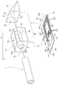
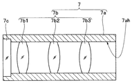
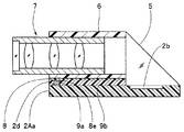
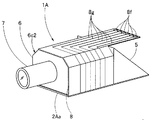
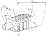
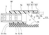
- the figure which shows the imaging device of 1st Embodiment. 1 is an exploded perspective view illustrating a configuration of an imaging apparatus according to a first embodiment. Longitudinal sectional view of the unit body of FIG. Exploded perspective view for explaining the configuration of the imaging apparatus of the second embodiment.
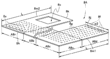
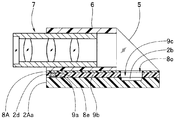
- the figure which shows the imaging device of 2nd Embodiment The figure explaining the other structural example of a flexible substrate The figure explaining the relationship between a prism and a light-receiving part in the state which mounted the flexible substrate, holding frame, and prism of FIG. 8 on the surface of the solid-state image sensor.
- Exploded perspective view for explaining the configuration of the imaging apparatus of the third embodiment The figure explaining the connection state of the electrode pad and pad connection electrode in the state which mounted the holding frame and the prism on the surface of the board
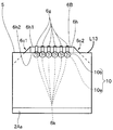
- 12 is an explanatory diagram when the imaging device of FIG. 12 is viewed from the arrow 13 side.
- the imaging device 1 of the present embodiment includes a solid-state imaging device 2 and an objective optical unit 3.
- the objective optical unit 3 is integrally fixed to a surface that is one surface side of a substrate 2a (described later) constituting the solid-state imaging device 2.
- one surface represents the front surface and the other surface represents the back surface.
- the solid-state imaging device 2 is configured by providing a light receiving portion 2b, a circuit portion 2c, and a plurality of electrode pads 2d on the surface of a substantially rectangular substrate 2a.
- the substrate 2a is made of, for example, silicon.
- the surface of the substrate 2a is divided into a circuit portion region A2c, a light receiving portion region A2b, and a terminal portion region A2d in order from the first short side 2S1 that is the distal end side of the substrate 2a toward the base end. Yes.
- the circuit portion 2c is provided at a predetermined position in the circuit portion region A2c
- the light receiving portion 2b is provided at a predetermined position in the light receiving portion region A2b
- a plurality of positions are provided at predetermined positions in the terminal portion region A2d.
- An electrode pad 2d is provided as a terminal.
- the plurality of electrode pads 2d are made of, for example, aluminum, and are arranged in the vicinity of the second short side 2S2 along the second short side 2S2 which is the base end side of the substrate 2a.
- the electrode pad 2d is used to input and output signals between the circuit unit 2c and a camera control unit (not shown) that is an external device.
- the light receiving unit 2b captures an optical image of the subject and generates an imaging signal.
- the light receiving unit 2b is configured in a predetermined size and shape with a plurality of photodiodes.
- the light receiving unit 2b includes a color filter (not shown) formed on the photodiode and a micro lens (not shown) formed on the color filter.
- the circuit unit 2c includes a driving / signal processing circuit that performs signal processing of the imaging signal generated by the light receiving unit 2b and generation of a driving signal that drives the light receiving unit 2b.
- This circuit includes, for example, a shift register, an output amplifier, an A / D converter, and a memory circuit.
- the light receiving portion 2b and the circuit portion 2c are electrically connected by a plurality of first wirings 2e1, and the circuit portion 2c and each electrode pad 2d are electrically connected by a second wiring 2e2.
- the plurality of first wirings 2e1 are wirings parallel to the long sides 2L1, 2L2 of the substrate 2a.
- the plurality of first wirings 2e1 are formed so as to fit between the first side 2b1 and the second side 2b2 of the light receiving portion 2b parallel to the long sides 2L1, 2L2 of the substrate 2a, and are parallel to the long sides 2L1, 2L2. It is formed so as to fit between the first side 2c1 and the second side 2c2 of the circuit portion 2c.
- the second wiring 2e2 is divided into two parts, a wiring arranged on the long side 2L1 side and a wiring arranged on the long side 2L2 side.
- One of the two divided second wirings 2e2 is formed so as to pass through between the long side 2L1 and the first side 2b1 of the light receiving portion 2b and then be connected to the corresponding electrode pad 2d.
- the other is formed so as to be connected to the corresponding electrode pad 2d after passing between the long side 2L2 and the second side 2b2 of the light receiving portion 2b.
- the objective optical unit 3 includes an objective lens unit 4 and a prism 5.
- the objective lens unit 4 includes a holding frame 6 and a unit main body 7.
- the unit body 7 includes a lens frame 7a and an objective lens group 7b.
- the lens frame 7a is, for example, a pipe shape and has an axial through hole 7ah.
- a plurality of optical lenses 7b1, 7b2, and 7b3 constituting the objective lens group 7b for forming an optical image of the subject are fixed at predetermined positions by, for example, bonding. ing.
- the number of optical lenses constituting the objective lens group 7b is not limited to three, and may be more or less.
- Reference numeral 7c denotes a lens cover.
- the holding frame 6 has a rectangular parallelepiped shape as shown in FIG. 2, for example, and is made of a light shielding material.
- the light shielding material is made of, for example, a metal or a resin containing a light shielding material such as carbon particles or a pigment.
- the holding frame 6 has an installation surface 6a disposed on the circuit part region A2c on the surface of the substrate 2a.
- the holding frame 6 is formed with a through hole 6b having a central axis parallel to the longitudinal axis direction into which the lens frame 7a is inserted.
- Reference numeral 6d is a side surface
- reference numeral 6e is a top surface.
- the width dimension of the installation surface 6a is the same as the short sides 2S1 and 2S2 of the substrate 2a.
- the length dimension of the holding frame 6 is such that the base end side 6r of the installation surface 6a is a predetermined position on the substrate 2a in a state where the front end side 6f of the installation surface 6a coincides with the first short side 2S1 of the substrate 2a. Specifically, it is set so as to cross, for example, an intermediate portion of the plurality of first wirings 2e1.
- Numerals 6c1 and 6c2 are chamfered portions and constitute a part of the side surface 6d.
- the chamfered portions 6c1 and 6c2 are so-called C-planes formed by planes.
- the chamfered portions 6c1 and 6c2 are not limited to the C surface, and may be so-called R surfaces configured by curved surfaces.
- the holding frame 6 may be configured without providing the chamfered portions 6c1 and 6c2.
- the prism 5 is made of glass, for example, and includes an entrance surface 5a, an exit surface 5b, and a reflection surface 5c as shown in FIG.
- the incident surface 5 a is disposed on the base end surface of the holding frame 6.
- the emission surface 5b is arranged in the light receiving part region A2b on the surface of the substrate 2a and covers the light receiving part 2b.
- the prism 5 bends an optical image that has passed through the objective lens unit 4 and is incident from the incident surface 5 a at a right angle, and guides the optical image to the light receiving unit 2 b of the solid-state imaging device 2.
- the width dimension of the prism 5 is the same as that of the short sides 2S1 and 2S2 of the substrate 2a, similarly to the width dimension of the installation surface 6a of the holding frame 6.
- the length dimension of the prism 5 is such that the base end side 5r constituting the exit surface 5b and the reflection surface 5c is at a predetermined position on the substrate 2a in a state where the incident surface 5a is disposed on the base end surface of the holding frame 6. It is set to be placed. As a result, the electrode pad 2d is exposed to the outside in a predetermined state.
- the installation surface 6a of the holding frame 6 is disposed on the circuit part region A2c on the surface of the substrate 2a, and is integrally bonded and fixed to the substrate 2a with, for example, a thermosetting adhesive.
- the circuit area A2c of the substrate 2a is supported by the holding frame 6.
- the emission surface 5b of the prism 5 is disposed on the light receiving area A2b on the surface of the substrate 2a, and is integrally bonded and fixed to the substrate 2a with, for example, an ultraviolet curable adhesive.
- the light receiving area A2b of the substrate 2a is supported by the prism 5.
- the adhesive that bonds the prism 5 and the substrate 2a desirably has a transmittance of 90% or more in the wavelength region of the light to be imaged.
- corresponding signal lines are electrically connected to the electrode pads 2d provided on the surface of the substrate 2a and exposed to the outside. Yes.
- the operator prepares the solid-state imaging device 2, the prism 5, the holding frame 6, the unit main body 7, and the like when assembling the imaging device 1. Next, the operator adheres and fixes the installation surface 6a of the holding frame 6 to, for example, the circuit area A2c on the substrate 2a of the solid-state imaging device 2.
- the operator places the incident surface of the prism 5 on the base end surface of the holding frame 6, and adheres and fixes the emission surface 5 b of the prism 5 to the heavy region A ⁇ b> 2 c on the substrate 2 a of the solid-state imaging device 2. As a result, the electrode pad 2d on the substrate 2a is exposed.
- the worker electrically connects a signal line (not shown) to the plurality of electrode pads 2d.
- the operator inserts the unit body 7 into the through hole 6 b of the holding frame 6.
- the operator then moves the unit body 7 back and forth in the longitudinal direction of the holding frame 6 to adjust the focus.
- the operator fixes the unit body 7 to the holding frame 6 by bonding or the like.
- the imaging device 1 shown in FIG. 1 is configured.
- the assembly procedure is not limited to the above-described order, and can be appropriately changed in consideration of workability.
- the holding frame 6 and the prism 5 are fixed at predetermined positions on the substrate 2a constituting the solid-state imaging device 2, and the plurality of electrode pads 2d arranged in the terminal portion region A2d are exposed to image.
- the apparatus 1 is configured. According to this configuration, the other region is supported by the holding frame 6 and the prism 5 while leaving the terminal region A2d of the substrate 2a constituting the solid-state imaging device 2. Accordingly, it is possible to greatly reduce the problem that cracks and cracks occur in the solid-state imaging device 2. As a result, it is possible to reduce the thickness of the solid-state imaging device 2 and reduce the size of the imaging device 1. In addition, since the small imaging device 1 can be easily handled, workability and yield can be improved.
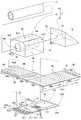
- FIG. 4 is an exploded perspective view illustrating the configuration of the imaging apparatus according to the second embodiment.
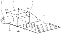
- FIG. 5 is a diagram illustrating the imaging apparatus according to the second embodiment.
- a flexible substrate, a holding frame, and a prism are provided on the surface of the substrate constituting the solid-state imaging device.
- FIG. 6 is a diagram illustrating a mounted state.
- FIG. 6 illustrates an electrode pad and a pad connection electrode in a state where a flexible substrate, a holding frame, and a prism are mounted on the surface of a substrate constituting a solid-state imaging device in the imaging device of the second embodiment.
- FIG. 7 is a diagram illustrating an image pickup apparatus according to the second embodiment, FIG.
- FIG. 8 is a diagram illustrating another example of the configuration of the flexible substrate
- FIG. 9 is a diagram of FIG. It is a figure explaining the relationship between a prism and the light-receiving part in the state which mounted the board
- the imaging apparatus 1A of the present embodiment includes a solid-state imaging device 2A, an objective optical unit 3, and a flexible substrate 8 as shown in FIG. As shown in FIG. 5, at least a part of the flexible substrate 8 is disposed between the surface of the substrate 2 ⁇ / b> Aa and the installation surface 6 a ⁇ b> 1 of the holding frame 6.
- the solid-state imaging device 2A of the present embodiment is provided with a light receiving unit 2b, a circuit unit 2c, and a plurality of electrode pads 2d on the surface of a substantially rectangular substrate 2Aa as in the first embodiment.
- the arrangement order of the respective regions from the first short side 2S1 side which is the front end side of the substrate 2Aa is different. That is, in the present embodiment, a terminal area A2d, a circuit area A2c, and a light receiving area A2b are provided in order from the first short side 2S1 side.
- the plurality of electrode pads 2d are arranged in the vicinity of the first short side 2S1 along the first short side 2S1 of the substrate 2Aa.
- each electrode pad 2d and the circuit portion 2c are electrically connected by a plurality of third wirings 2e3 parallel to the long sides 2L1, 2L2 of the substrate 2Aa, like the first wiring 2e1.
- the third wiring 2e3 is formed so as to fit between the first side 2c1 and the second side 2c2 of the circuit unit 2c parallel to the long sides 2L1, 2L2 of the substrate 2Aa.
- the flexible substrate 8 is made of polyimide, for example, and has an L shape.
- the surface which is one surface of the flexible substrate 8 is divided into an installation surface region A8a, a side surface region A8b, a top surface region A8c, and a connection region A8d.
- the installation surface 6a1 of the holding frame 6 is arranged and fixed in the installation surface area A8a.
- the side surface region A8b is disposed and fixed to the side surface 6d and the chamfered portion 6c1 of the holding frame 6.
- the top surface area A8c is arranged and fixed on the top surface 6e of the holding frame 6.
- the connection area A8d is disposed so as to protrude further from the base end side 6er of the holding frame 6 to the base end side.
- a plurality of pad connection electrodes 8e, a plurality of signal line connection electrodes 8f, and a plurality of wirings 8g are provided at predetermined positions on the back surface, which is the other surface of the flexible substrate 8.
- the plurality of pad connection electrodes 8e are first electrodes that are electrically connected to the plurality of electrode pads 2d arranged in the terminal area A2d of the substrate 2Aa.
- the plurality of pad connection electrodes 8e are arranged on the back surface of the installation surface area A8a in the vicinity of the front end side 8h along the front end side 8h constituting the installation surface area A8a.
- the plurality of signal line connection electrodes 8f are second electrodes to which corresponding signal lines (not shown) are electrically connected.
- the plurality of signal line connection electrodes 8f are arranged on the back surface of the connection region A8d near the base end side 8j along the base end side 8j constituting the connection region A8d.
- the plurality of pad connection electrodes 8e and the plurality of signal line connection electrodes 8f are electrically connected by a plurality of wirings 8g, respectively.
- the plurality of wirings 8g are provided at predetermined positions on the back surface of the installation surface region A8a, the back surface of the side surface region A8b, the back surface of the top surface region A8c, and the back surface of the connection region A8d.
- the first width dimension w1 of the flexible substrate 8 is such that the opposite side 8k facing the front end side 8h is formed on the substrate 2Aa in a state where the front end side 8h of the flexible substrate 8 coincides with the first short side 2S1 of the substrate 2Aa. It is set so as to cross an intermediate portion of the plurality of first wirings 2e1.
- the width dimension (second width dimension) w2 of the base end side 8j facing the front end side 8h of the flexible substrate 8 is set to the same size as the base end side 6er of the top surface 6e.
- the length dimension of the first side 8m1 of the flexible substrate 8 is set to a dimension L that is substantially the same as the length dimension of the substrate 2Aa.
- the imaging apparatus 1A of the present embodiment is assembled in the following procedure.
- the operator prepares the solid-state imaging device 2A, the prism 5, the holding frame 6, the unit body 7, the flexible substrate 8, and the like.
- the operator places the installation surface 6a1 of the holding frame 6 on the installation surface area A8a of the flexible substrate 8. At this time, the operator matches the front end side 6f of the holding frame 6 with the front end side 8h of the flexible substrate 8 and matches the long side 6L2 of the holding frame 6 with the second side side 8m2 of the flexible substrate 8. Thereafter, the operator integrally fixes the flexible substrate 8 and the holding frame 6 with, for example, a thermosetting adhesive.
- the operator places the back surface of the flexible substrate 8 integrated with the holding frame 6 on the terminal area A2d and the circuit area A2c of the substrate 2Aa of the solid-state imaging device 2A.
- the installation surface area A8a portion which is a part of the flexible substrate 8 is arranged between the surface of the substrate 2Aa and the installation surface 6a1 of the holding frame 6A.
- the installation surface 6a1 is disposed on the terminal part region A2d and the circuit part region A2c on the surface of the substrate 2Aa via the flexible substrate 8.
- the operator matches the tip side 8h of the flexible substrate 8 with the first short side 2S1 of the substrate 2Aa, and matches the second side 8m2 of the flexible substrate 8 with the long side 2L2 of the substrate 2Aa.
- the worker sets the plurality of electrode pads 2d and the plurality of pad connection electrodes 8e to face each other and connects the electrode pads 2d and the plurality of pad connection electrodes 8e electrically.
- Gold bumps 9a as members are arranged in a predetermined state.
- the operator integrally fixes the substrate 2Aa and the flexible substrate 8 with an adhesive.
- the electrode pad 2d and the plurality of pad connection electrodes 8e are electrically connected through the gold bumps 9a.
- Reference numeral 9b denotes an adhesive layer.
- the above-described adhesive is, for example, a thermosetting adhesive.
- the connecting member is not limited to the gold bump 9a, and may be a solder bump or the like.
- the operator places the incident surface of the prism 5 on the base end surface of the holding frame 6 as shown in FIG. 5, and places the emission surface 5 b of the prism 5 on the light receiving part region A ⁇ b> 2 b of the substrate 2 ⁇ / b> Aa of the solid-state imaging device 2 ⁇ / b> A, for example. Integrate with UV curable adhesive.
- the entire surface of the substrate 2Aa is supported by the holding frame 6 and the prism 5 of the objective lens unit 4 constituting the objective optical unit 3.
- the operator bends the flexible substrate 8 extending from the substrate 2Aa, arranges the side surface region A8b of the flexible substrate 8 on the side surface 6d and the chamfered portion 6c1 of the holding frame 6, and The surface area A8c is arranged on the top surface 6e of the holding frame 6.
- the worker integrally fixes the side surface region A8b to the side surface 6d and the chamfered portion 6c1, and fixes the top surface region A8c to the top surface 6e, for example, with a thermosetting adhesive, as shown in FIG.
- the operator inserts the unit main body 7 into the through hole 6b of the holding frame 6.
- the operator then moves the unit body 7 back and forth in the longitudinal direction of the holding frame 6 to adjust the focus.
- the operator integrally fixes the unit body 7 to the holding frame 6 by bonding or the like.
- an imaging apparatus 1A in which the connection area A8d of the flexible substrate 8 protrudes toward the proximal end side of the holding frame 6 as shown in FIG.
- the signal line is each electrically connected to the some signal line connection electrode 8f.
- the assembly procedure is not limited to the above-described order, and can be appropriately changed in consideration of workability.
- the holding frame 6 and the prism 5 of the objective lens unit 4 constituting the objective optical unit 3 are fixed to the entire surface of the substrate 2Aa constituting the solid-state image pickup device 2 via the flexible substrate 8, and the imaging device 1A is fixed. Constitute. According to this configuration, since the entire region of the substrate 2Aa is supported by the holding frame 6 and the prism 5, it is possible to solve the problem that the solid-state imaging device 2 is cracked and broken. As a result, the workability of the small-sized imaging device 1 can be greatly improved and the yield can be greatly improved.
- the flexible substrate 8 extending from the holding frame 6 is integrally fixed to the side surface 6d, the chamfered portion 6c1, and the top surface 6e of the holding frame 6 to reliably prevent the imaging device 1A from becoming large. it can.
- the long side 2L1 and the first side 2b1 of the light receiving unit 2b, and the long side 2L2 and the light receiving unit like the substrate 2a of the first embodiment.
- the image pickup apparatus can be further downsized.
- an electrode for mounting components may be provided between the wirings of the flexible substrate 8 and an electronic component such as a chip capacitor may be mounted on the electrodes.
- the flexible substrate 8 is not limited to the embodiment described above, and may be a flexible substrate 8A shown in FIG.
- the flexible substrate 8A shown in FIG. 8 is divided on the surface into an objective optical part region A8n, a side surface region A8b, a top surface region A8c, and a connection region A8d.
- the installation surface 6a1 of the holding frame 6 is arranged and fixed in the objective optical part region A8n, and the emission surface 5b of the prism 5 is arranged and fixed.
- the length dimension of the objective optical part region A8n is set to a dimension L that is substantially the same as the length dimension of the substrate 2Aa. That is, the objective optical part region A8n is arranged on the entire surface of the substrate 2Aa. Therefore, an opening 8o for opening the light receiving part 2b provided on the substrate 2Aa is formed at a predetermined position of the objective optical part area A8n.
- the installation surface area A8a of the holding frame 6 and the emission surface 5b of the prism 5 are arranged on the surface of the objective optical part area A8n, and are fixed integrally with an adhesive.
- Reference numeral 9c denotes a gap, which is formed on the adhesive layer 9b.
- the entire surface area of the substrate 2Aa is supported by the holding frame 6 and the prism 5 via the flexible substrate 8A as shown in FIG. Can be eliminated.
- FIG. 10 is a diagram illustrating an imaging apparatus according to the third embodiment
- FIG. 11 is an exploded perspective view illustrating the configuration of the imaging apparatus according to the third embodiment
- FIG. 12 is a holding frame on the surface of the substrate that configures the solid-state imaging device
- FIG. 13 is a diagram for explaining the connection relationship between the electrode pad and the pad connection electrode and the connection state between the second contact and the signal line in a state where the prism is mounted.
- FIG. 13 is a diagram when the imaging device of FIG. 12 is viewed from the arrow 13 side.
- FIG. In the following description of the third embodiment the same components as those in the above-described embodiment are denoted by the same reference numerals and description thereof is omitted.
- the imaging apparatus 1B of the present embodiment includes a solid-state imaging device 2A and an objective optical unit 3B.
- the objective optical unit 3B includes an objective lens unit 4B and a prism 5.
- the objective lens unit 4B includes a holding frame 6B and a unit main body 7.
- Reference numeral 6g is a three-dimensional wiring.
- the holding frame 6B has a substantially rectangular parallelepiped shape and has a flange portion 6h.
- the flange portion 6h is a convex portion that protrudes a predetermined distance in the longitudinal axis direction from the base end side 6er of the top surface 6e of the holding frame 6B.
- the first surface 6h1 and the top surface 6e of the flange 6h are the same plane.
- the holding frame 6B has an installation surface 6a1 disposed on the terminal part region A2d and the circuit part region A2c on the surface of the substrate 2Aa.
- a through hole 6b is formed in the holding frame 6B.
- the holding frame 6B is made of, for example, a resin having a light shielding property and an insulating property.
- Reference numerals 6c1 and 6c2 are chamfered portions, and reference numeral 6d1 is a first side surface.
- a plurality of first contacts 6j are arranged on the installation surface 6a1 of the holding frame 6B along the front end side 6f and arranged in the vicinity of the front end side 6f.
- the first contact 6j is electrically connected to a plurality of electrode pads 2d provided in the terminal area A2d of the substrate 2Aa.
- a plurality of second contacts 6k are provided on the second surface 6h2 of the flange 6h of the holding frame 6B.
- the second contact 6k is used when signals are input / output between the circuit unit 2c of the substrate 2Aa and the external device via the first contact 6j.
- the second surface 6h2 is a surface facing the first surface 6h1, in other words, the back surface of the first surface 6h1.
- the plurality of second contacts 6k are arranged in the vicinity of the base end side 6hr along the base end side 6hr of the flange portion 6h.
- the three-dimensional wiring 6g is provided on the installation surface 6a1, the first side surface 6d1, the first chamfered portion 6c1, the top surface 6e, the first surface 6h1 of the flange portion 6h, the base end surface 6h3, and the second surface 6h2 of the flange portion 6h. Is provided.
- the three-dimensional wiring 6g electrically connects the plurality of first contacts 6j and the plurality of second contacts 6k, respectively.
- the imaging device 1B of the present embodiment is assembled by the following procedure.
- the operator prepares the solid-state imaging device 2A, the prism 5, the holding frame 6B, the unit main body 7, and the like when assembling the imaging device 1B.
- the operator places the installation surface 6a1 of the holding frame 6B on the terminal area A2d and the circuit area A2c of the substrate 2Aa of the solid-state imaging device 2A.
- the operator sets the plurality of electrode pads 2d and the plurality of first contacts 6j to face each other and connects the electrode pads 2d and the plurality of first contacts 6j electrically.
- Gold bumps 9a as members are arranged in a predetermined state.
- the operator integrally fixes the substrate 2Aa and the holding frame 6B with an adhesive.
- the electrode pad 2d and the plurality of first contacts 6j are electrically connected via the gold bump 9a.
- Reference numeral 9b denotes an adhesive layer.
- the adhesive an insulating thermosetting adhesive is used.
- the operator arranges the incident surface of the prism 5 on the base end surface of the holding frame 6, and places the emission surface 5 b of the prism 5 on the light receiving part region A ⁇ b> 2 b of the substrate 2 ⁇ / b> Aa of the solid-state imaging device 2 ⁇ / b> A with, for example, an ultraviolet curable adhesive. Fix together.
- the entire surface of the substrate 2Aa is supported by the holding frame 6B and the prism 5 of the objective lens unit 4 constituting the objective optical unit 3.
- the worker connects the core wires 10a of the plurality of signal lines 10 to the second contacts 6k, respectively.
- the operator inserts the unit main body 7 into the through-hole 6b of the holding frame 6, adjusts the focus, and adheres and fixes to the holding frame 6.
- the imaging apparatus 1B shown in FIG. 10 is configured.
- the imaging device 1B is configured by fixing the holding frame 6B and the prism 5 of the objective lens unit 4 constituting the objective optical unit 3 to the entire surface of the substrate 2Aa constituting the solid-state imaging device 2A.
- the problem that cracks and cracks occur in the image sensor 2 can be solved.
- the first contact 6j, the second contact 6k, and the three-dimensional wiring 6g for connecting the first contact 6j and the second contact 6k are provided on the holding frame 6B, thereby eliminating the need for the flexible substrate 8 and reducing the number of components. In addition, the number of assembly steps can be reduced.
- the outer sheath 10b of the signal line 10 having the core wire 10a connected to the second contact 6k as shown in FIG. Is within the side surface outline indicated by the very thick line L13 of the imaging device 1B.
- an electronic component such as a chip capacitor may be mounted on the second surface 6h2 of the flange 6h.
- the holding frame 6 is provided with a flange, the connection region A8d of the flexible substrate 8 is bent on the second surface of the flange, and the signal line connection electrode 8f is formed on the second surface. It may be arranged. According to this configuration, by connecting the signal line to the signal line connection electrode 8f that is bent and disposed on the second surface of the collar portion, the signal line is disposed outside the side surface outline of the imaging device 1A. An increase in the outer shape of 1A is prevented.
Landscapes
- Health & Medical Sciences (AREA)
- Life Sciences & Earth Sciences (AREA)
- Surgery (AREA)
- Biomedical Technology (AREA)
- Medical Informatics (AREA)
- Optics & Photonics (AREA)
- Pathology (AREA)
- Radiology & Medical Imaging (AREA)
- Biophysics (AREA)
- Engineering & Computer Science (AREA)
- Physics & Mathematics (AREA)
- Heart & Thoracic Surgery (AREA)
- Nuclear Medicine, Radiotherapy & Molecular Imaging (AREA)
- Molecular Biology (AREA)
- Animal Behavior & Ethology (AREA)
- General Health & Medical Sciences (AREA)
- Public Health (AREA)
- Veterinary Medicine (AREA)
- Endoscopes (AREA)
- Studio Devices (AREA)
- Instruments For Viewing The Inside Of Hollow Bodies (AREA)
- Transforming Light Signals Into Electric Signals (AREA)
Abstract
L'invention concerne un dispositif d'imagerie qui comprend un dispositif d'imagerie à semi-conducteurs et une unité optique d'objectifs. Le dispositif d'imagerie à semi-conducteurs comprend un substrat, dont une surface est découpée en : une région d'unité de réception de lumière dans laquelle une unité de réception de lumière est disposée, laquelle génère un signal d'imagerie d'une image optique capturée d'un sujet ; une région d'unité de circuit dans laquelle une unité de circuit est disposée, laquelle réalise un traitement de signal du signal d'imagerie généré dans l'unité de réception de lumière et génère un signal de commande pour commander l'unité de réception de lumière ; et une région d'unité de terminal dans laquelle une pluralité de terminaux sont disposés, lesquels sont utilisés lorsque des signaux sont échangés entre l'unité de circuit et un dispositif externe. L'unité optique d'objectifs comprend : une unité d'objectifs comprenant un corps principal unitaire équipé d'un groupe d'objectifs pour former une image optique du sujet et un cadre de maintien sur lequel le corps principal unitaire est maintenu de manière fixe ; et un prisme pour courber l'axe optique du corps principal unitaire et guider l'image optique passant à travers l'unité d'objectifs dans l'unité de réception de lumière du dispositif d'imagerie à semi-conducteurs. Le prisme de l'unité optique d'objectifs est disposé sur la région d'unité de réception de lumière du substrat, et le cadre de maintien constituant l'unité d'objectifs de l'unité optique d'objectifs est disposé sur la région d'unité de circuit.
Priority Applications (2)
| Application Number | Priority Date | Filing Date | Title |
|---|---|---|---|
| EP12797267.7A EP2719319A4 (fr) | 2011-06-08 | 2012-06-01 | Dispositif d'imagerie |
| US14/088,800 US9967486B2 (en) | 2011-06-08 | 2013-11-25 | Image pickup apparatus |
Applications Claiming Priority (2)
| Application Number | Priority Date | Filing Date | Title |
|---|---|---|---|
| JP2011-128619 | 2011-06-08 | ||
| JP2011128619A JP6210656B2 (ja) | 2011-06-08 | 2011-06-08 | 撮像装置 |
Related Child Applications (1)
| Application Number | Title | Priority Date | Filing Date |
|---|---|---|---|
| US14/088,800 Continuation US9967486B2 (en) | 2011-06-08 | 2013-11-25 | Image pickup apparatus |
Publications (1)
| Publication Number | Publication Date |
|---|---|
| WO2012169444A1 true WO2012169444A1 (fr) | 2012-12-13 |
Family
ID=47296010
Family Applications (1)
| Application Number | Title | Priority Date | Filing Date |
|---|---|---|---|
| PCT/JP2012/064289 Ceased WO2012169444A1 (fr) | 2011-06-08 | 2012-06-01 | Dispositif d'imagerie |
Country Status (4)
| Country | Link |
|---|---|
| US (1) | US9967486B2 (fr) |
| EP (1) | EP2719319A4 (fr) |
| JP (1) | JP6210656B2 (fr) |
| WO (1) | WO2012169444A1 (fr) |
Cited By (4)
| Publication number | Priority date | Publication date | Assignee | Title |
|---|---|---|---|---|
| CN106061360A (zh) * | 2014-03-03 | 2016-10-26 | 奥林巴斯株式会社 | 摄像装置和内窥镜装置 |
| US9706903B2 (en) | 2009-06-18 | 2017-07-18 | Endochoice, Inc. | Multiple viewing elements endoscope system with modular imaging units |
| EP3013209A4 (fr) * | 2013-06-28 | 2017-08-02 | EndoChoice, Inc. | Système endoscope à plusieurs éléments de visualisation doté d'unités d'imagerie modulaires |
| US10571680B2 (en) | 2015-01-23 | 2020-02-25 | Olympus Corporation | Image pickup apparatus and endoscope |
Families Citing this family (14)
| Publication number | Priority date | Publication date | Assignee | Title |
|---|---|---|---|---|
| DE112014000800T5 (de) | 2013-02-13 | 2015-10-29 | Fujikura Ltd. | Bildgebungsmodul, isolierrohrbefestigtes Bildgebungsmodul, linsenbefestigtes Bildgebungsmodul und Endoskop |
| JP5722513B1 (ja) * | 2013-09-25 | 2015-05-20 | オリンパスメディカルシステムズ株式会社 | 電気ユニット、及びこれを搭載した内視鏡 |
| JP6329394B2 (ja) * | 2014-03-03 | 2018-05-23 | オリンパス株式会社 | 撮像装置、および内視鏡装置 |
| CN106102552A (zh) * | 2014-03-28 | 2016-11-09 | 富士胶片株式会社 | 内窥镜用摄像装置 |
| JP2016177195A (ja) * | 2015-03-20 | 2016-10-06 | 株式会社リコー | マイクロレンズ基板及び撮像装置 |
| CN107529964A (zh) * | 2015-05-28 | 2018-01-02 | 奥林巴斯株式会社 | 摄像装置和内窥镜系统 |
| EP3369359A4 (fr) * | 2015-10-27 | 2019-06-05 | Olympus Corporation | Dispositif d'imagerie et endoscope |
| US10524643B2 (en) * | 2017-11-06 | 2020-01-07 | Karl Storz Endovision, Inc. | Image sensor module with turning prism |
| JP7132007B2 (ja) * | 2018-07-18 | 2022-09-06 | i-PRO株式会社 | 内視鏡用撮像ユニットおよび内視鏡 |
| DE102018126795A1 (de) * | 2018-10-26 | 2020-04-30 | Hoya Corporation | Endoskop mit Platine |
| CN115804093A (zh) * | 2020-06-03 | 2023-03-14 | 诺基亚技术有限公司 | 用于视频编码和视频解码的方法、装置和计算机程序产品 |
| US12013521B2 (en) * | 2020-06-29 | 2024-06-18 | Mgi Tech Co., Ltd. | Systems and methods for optical scanning and imaging through a fluid medium for nucleic acid sequencing |
| US11759095B2 (en) * | 2021-08-29 | 2023-09-19 | Altek Biotechnology Corporation | Image capturing assembly and related endoscope |
| US12560480B2 (en) | 2022-11-08 | 2026-02-24 | Mgi Tech Co., Ltd. | Immersion imaging systems and methods for flowcells |
Citations (10)
| Publication number | Priority date | Publication date | Assignee | Title |
|---|---|---|---|---|
| JPS6235314U (fr) * | 1985-08-16 | 1987-03-02 | ||
| JPS63177106A (ja) * | 1986-09-01 | 1988-07-21 | Olympus Optical Co Ltd | 内視鏡 |
| JPH1033474A (ja) * | 1996-07-23 | 1998-02-10 | Olympus Optical Co Ltd | 電子内視鏡 |
| JP2000019427A (ja) * | 1998-07-06 | 2000-01-21 | Fuji Photo Optical Co Ltd | 内視鏡用撮像素子組付けユニット |
| JP2002136474A (ja) * | 2000-11-02 | 2002-05-14 | Olympus Optical Co Ltd | 内視鏡 |
| JP2006141884A (ja) * | 2004-11-24 | 2006-06-08 | Fujinon Corp | 電子内視鏡用撮像装置 |
| JP2008118568A (ja) * | 2006-11-07 | 2008-05-22 | Olympus Medical Systems Corp | 撮像装置 |
| JP2009268639A (ja) * | 2008-05-02 | 2009-11-19 | Olympus Corp | カプセル型内視鏡 |
| JP2009288682A (ja) | 2008-05-30 | 2009-12-10 | Olympus Medical Systems Corp | 内視鏡対物光学系 |
| JP2010069186A (ja) * | 2008-09-22 | 2010-04-02 | Fujifilm Corp | 撮像装置及び内視鏡 |
Family Cites Families (10)
| Publication number | Priority date | Publication date | Assignee | Title |
|---|---|---|---|---|
| US3499107A (en) * | 1954-03-11 | 1970-03-03 | Sheldon Edward E | Light transfer devices using light conducting members of multilayered construction and photoelectric means |
| US4622954A (en) * | 1984-05-15 | 1986-11-18 | Fuji Photo Optical Co., Ltd. | Endoscope having a plate-like image sensor for forming images |
| US4646721A (en) * | 1984-06-26 | 1987-03-03 | Fuji Photo Optical Co., Ltd. | Light shielding construction for the forward end of an endoscope |
| US4832003A (en) * | 1986-09-12 | 1989-05-23 | Olympus Optical Co., Ltd. | Electronic endoscope tip |
| AU2003299805A1 (en) * | 2002-12-20 | 2004-07-22 | Itac Systems, Inc. | Cursor control device |
| US7300397B2 (en) * | 2004-07-29 | 2007-11-27 | C2C Cure, Inc. | Endoscope electronics assembly |
| US8179428B2 (en) | 2004-11-24 | 2012-05-15 | Fujinon Corporation | Imaging apparatus for electronic endoscope and electronic endoscope |
| JP4917060B2 (ja) * | 2007-02-26 | 2012-04-18 | Hoya株式会社 | 撮像ユニット及び携帯用電子機器 |
| JP2010051538A (ja) * | 2008-08-28 | 2010-03-11 | Panasonic Corp | 撮像装置 |
| US20130317529A1 (en) * | 2010-12-03 | 2013-11-28 | Steven S. Golden | Methods and devices for metabolic surgery |
-
2011
- 2011-06-08 JP JP2011128619A patent/JP6210656B2/ja active Active
-
2012
- 2012-06-01 EP EP12797267.7A patent/EP2719319A4/fr not_active Withdrawn
- 2012-06-01 WO PCT/JP2012/064289 patent/WO2012169444A1/fr not_active Ceased
-
2013
- 2013-11-25 US US14/088,800 patent/US9967486B2/en not_active Expired - Fee Related
Patent Citations (10)
| Publication number | Priority date | Publication date | Assignee | Title |
|---|---|---|---|---|
| JPS6235314U (fr) * | 1985-08-16 | 1987-03-02 | ||
| JPS63177106A (ja) * | 1986-09-01 | 1988-07-21 | Olympus Optical Co Ltd | 内視鏡 |
| JPH1033474A (ja) * | 1996-07-23 | 1998-02-10 | Olympus Optical Co Ltd | 電子内視鏡 |
| JP2000019427A (ja) * | 1998-07-06 | 2000-01-21 | Fuji Photo Optical Co Ltd | 内視鏡用撮像素子組付けユニット |
| JP2002136474A (ja) * | 2000-11-02 | 2002-05-14 | Olympus Optical Co Ltd | 内視鏡 |
| JP2006141884A (ja) * | 2004-11-24 | 2006-06-08 | Fujinon Corp | 電子内視鏡用撮像装置 |
| JP2008118568A (ja) * | 2006-11-07 | 2008-05-22 | Olympus Medical Systems Corp | 撮像装置 |
| JP2009268639A (ja) * | 2008-05-02 | 2009-11-19 | Olympus Corp | カプセル型内視鏡 |
| JP2009288682A (ja) | 2008-05-30 | 2009-12-10 | Olympus Medical Systems Corp | 内視鏡対物光学系 |
| JP2010069186A (ja) * | 2008-09-22 | 2010-04-02 | Fujifilm Corp | 撮像装置及び内視鏡 |
Non-Patent Citations (1)
| Title |
|---|
| See also references of EP2719319A4 |
Cited By (7)
| Publication number | Priority date | Publication date | Assignee | Title |
|---|---|---|---|---|
| US9706903B2 (en) | 2009-06-18 | 2017-07-18 | Endochoice, Inc. | Multiple viewing elements endoscope system with modular imaging units |
| US10092167B2 (en) | 2009-06-18 | 2018-10-09 | Endochoice, Inc. | Multiple viewing elements endoscope system with modular imaging units |
| US10791910B2 (en) | 2009-06-18 | 2020-10-06 | Endochoice, Inc. | Multiple viewing elements endoscope system with modular imaging units |
| EP3013209A4 (fr) * | 2013-06-28 | 2017-08-02 | EndoChoice, Inc. | Système endoscope à plusieurs éléments de visualisation doté d'unités d'imagerie modulaires |
| CN106061360A (zh) * | 2014-03-03 | 2016-10-26 | 奥林巴斯株式会社 | 摄像装置和内窥镜装置 |
| US10416438B2 (en) | 2014-03-03 | 2019-09-17 | Olympus Corporation | Imaging device for imaging inside of subject and endoscope device using the same |
| US10571680B2 (en) | 2015-01-23 | 2020-02-25 | Olympus Corporation | Image pickup apparatus and endoscope |
Also Published As
| Publication number | Publication date |
|---|---|
| US9967486B2 (en) | 2018-05-08 |
| JP2012254176A (ja) | 2012-12-27 |
| JP6210656B2 (ja) | 2017-10-11 |
| US20140078280A1 (en) | 2014-03-20 |
| EP2719319A4 (fr) | 2015-03-11 |
| EP2719319A1 (fr) | 2014-04-16 |
Similar Documents
| Publication | Publication Date | Title |
|---|---|---|
| JP6210656B2 (ja) | 撮像装置 | |
| JP5839811B2 (ja) | 撮像ユニット及び内視鏡 | |
| JP5767414B2 (ja) | 内視鏡用撮像ユニット | |
| US11000184B2 (en) | Image pickup module, fabrication method for image pickup module, and endoscope | |
| US11435570B2 (en) | Image pickup apparatus for endoscope, endoscope, and manufacturing method of image pickup apparatus for endoscope | |
| WO2018173323A1 (fr) | Endoscope | |
| JP5722512B1 (ja) | 内視鏡用撮像ユニット | |
| JP5425353B1 (ja) | 内視鏡用撮像ユニット及び内視鏡 | |
| JP5715024B2 (ja) | 撮像ユニット、内視鏡及び撮像ユニットの製造方法 | |
| US9629524B2 (en) | Image pickup unit for endoscope having first and second leads with differing distances to image pickup device | |
| US11179025B2 (en) | Image pickup apparatus and endoscope | |
| JP2008528094A (ja) | 狭い組立て外形を持つセンサ | |
| JP4709661B2 (ja) | 撮像装置 | |
| JPH1176156A (ja) | 撮像装置 | |
| JP7702341B2 (ja) | 内視鏡撮像装置及び内視鏡 | |
| JPH09307087A (ja) | 固体撮像装置 | |
| WO2015145859A1 (fr) | Dispositif d'imagerie endoscopique | |
| JPH10146312A (ja) | 撮像装置 | |
| US12309479B2 (en) | Image pickup module and endoscope | |
| JP7592553B2 (ja) | 内視鏡撮像装置および内視鏡 | |
| JP4699741B2 (ja) | 内視鏡用撮像装置 | |
| JP2013000241A (ja) | 撮像装置 | |
| JP2012186677A (ja) | 光学デバイス及びその製造方法 |
Legal Events
| Date | Code | Title | Description |
|---|---|---|---|
| 121 | Ep: the epo has been informed by wipo that ep was designated in this application |
Ref document number: 12797267 Country of ref document: EP Kind code of ref document: A1 |
|
| NENP | Non-entry into the national phase |
Ref country code: DE |