WO2012176473A1 - Substrat semi-conducteur ayant des marquages de points, et son procédé de production - Google Patents
Substrat semi-conducteur ayant des marquages de points, et son procédé de production Download PDFInfo
- Publication number
- WO2012176473A1 WO2012176473A1 PCT/JP2012/004073 JP2012004073W WO2012176473A1 WO 2012176473 A1 WO2012176473 A1 WO 2012176473A1 JP 2012004073 W JP2012004073 W JP 2012004073W WO 2012176473 A1 WO2012176473 A1 WO 2012176473A1
- Authority
- WO
- WIPO (PCT)
- Prior art keywords
- semiconductor substrate
- dot
- recess
- recesses
- manufacturing
- Prior art date
- Legal status (The legal status is an assumption and is not a legal conclusion. Google has not performed a legal analysis and makes no representation as to the accuracy of the status listed.)
- Ceased
Links
Images


Classifications
-
- G—PHYSICS
- G03—PHOTOGRAPHY; CINEMATOGRAPHY; ANALOGOUS TECHNIQUES USING WAVES OTHER THAN OPTICAL WAVES; ELECTROGRAPHY; HOLOGRAPHY
- G03F—PHOTOMECHANICAL PRODUCTION OF TEXTURED OR PATTERNED SURFACES, e.g. FOR PRINTING, FOR PROCESSING OF SEMICONDUCTOR DEVICES; MATERIALS THEREFOR; ORIGINALS THEREFOR; APPARATUS SPECIALLY ADAPTED THEREFOR
- G03F9/00—Registration or positioning of originals, masks, frames, photographic sheets or textured or patterned surfaces, e.g. automatically
- G03F9/70—Registration or positioning of originals, masks, frames, photographic sheets or textured or patterned surfaces, e.g. automatically for microlithography
- G03F9/7003—Alignment type or strategy, e.g. leveling, global alignment
- G03F9/7007—Alignment other than original with workpiece
-
- H—ELECTRICITY
- H10—SEMICONDUCTOR DEVICES; ELECTRIC SOLID-STATE DEVICES NOT OTHERWISE PROVIDED FOR
- H10D—INORGANIC ELECTRIC SEMICONDUCTOR DEVICES
- H10D62/00—Semiconductor bodies, or regions thereof, of devices having potential barriers
- H10D62/10—Shapes, relative sizes or dispositions of the regions of the semiconductor bodies; Shapes of the semiconductor bodies
-
- H—ELECTRICITY
- H10—SEMICONDUCTOR DEVICES; ELECTRIC SOLID-STATE DEVICES NOT OTHERWISE PROVIDED FOR
- H10F—INORGANIC SEMICONDUCTOR DEVICES SENSITIVE TO INFRARED RADIATION, LIGHT, ELECTROMAGNETIC RADIATION OF SHORTER WAVELENGTH OR CORPUSCULAR RADIATION
- H10F77/00—Constructional details of devices covered by this subclass
-
- H—ELECTRICITY
- H10—SEMICONDUCTOR DEVICES; ELECTRIC SOLID-STATE DEVICES NOT OTHERWISE PROVIDED FOR
- H10P—GENERIC PROCESSES OR APPARATUS FOR THE MANUFACTURE OR TREATMENT OF DEVICES COVERED BY CLASS H10
- H10P50/00—Etching of wafers, substrates or parts of devices
- H10P50/60—Wet etching
- H10P50/64—Wet etching of semiconductor materials
- H10P50/642—Chemical etching
-
- H—ELECTRICITY
- H10—SEMICONDUCTOR DEVICES; ELECTRIC SOLID-STATE DEVICES NOT OTHERWISE PROVIDED FOR
- H10W—GENERIC PACKAGES, INTERCONNECTIONS, CONNECTORS OR OTHER CONSTRUCTIONAL DETAILS OF DEVICES COVERED BY CLASS H10
- H10W46/00—Marks applied to devices, e.g. for alignment or identification
-
- H—ELECTRICITY
- H10—SEMICONDUCTOR DEVICES; ELECTRIC SOLID-STATE DEVICES NOT OTHERWISE PROVIDED FOR
- H10W—GENERIC PACKAGES, INTERCONNECTIONS, CONNECTORS OR OTHER CONSTRUCTIONAL DETAILS OF DEVICES COVERED BY CLASS H10
- H10W46/00—Marks applied to devices, e.g. for alignment or identification
- H10W46/101—Marks applied to devices, e.g. for alignment or identification characterised by the type of information, e.g. logos or symbols
- H10W46/106—Marks applied to devices, e.g. for alignment or identification characterised by the type of information, e.g. logos or symbols digital information, e.g. bar codes
-
- H—ELECTRICITY
- H10—SEMICONDUCTOR DEVICES; ELECTRIC SOLID-STATE DEVICES NOT OTHERWISE PROVIDED FOR
- H10W—GENERIC PACKAGES, INTERCONNECTIONS, CONNECTORS OR OTHER CONSTRUCTIONAL DETAILS OF DEVICES COVERED BY CLASS H10
- H10W46/00—Marks applied to devices, e.g. for alignment or identification
- H10W46/401—Marks applied to devices, e.g. for alignment or identification for identification or tracking
-
- H—ELECTRICITY
- H10—SEMICONDUCTOR DEVICES; ELECTRIC SOLID-STATE DEVICES NOT OTHERWISE PROVIDED FOR
- H10W—GENERIC PACKAGES, INTERCONNECTIONS, CONNECTORS OR OTHER CONSTRUCTIONAL DETAILS OF DEVICES COVERED BY CLASS H10
- H10W46/00—Marks applied to devices, e.g. for alignment or identification
- H10W46/501—Marks applied to devices, e.g. for alignment or identification for use before dicing
Definitions
- the present invention relates to a semiconductor substrate having dot marking and a manufacturing method thereof.
- the semiconductor substrate having the dot marking of the present invention is not particularly limited, but can be used as a semiconductor substrate for solar cells.
- Patent Document 4 It is also known to form a processing mark by etching the semiconductor crystal substrate in order to align the crystal orientation of the semiconductor crystal substrate with the alignment mark formed on the mask.
- Patent Document 4 it has been proposed to form a microwell chip by forming a microwell having an inverted conical shape or other shape on a silicon substrate (see Patent Documents 5 and 6).
- Patent Documents 7, 8, 9, and 10 a method of manufacturing a microprobe or microtip that includes a step of forming a recess in a single crystal silicon substrate is known (see Patent Documents 7, 8, 9, and 10).
- Patent Document 11 a method for forming a mark made of a dot hole on a silicon substrate for marking the silicon substrate. It is also known to form an inverted pyramid pattern on a silicon substrate and use the pattern as a marking (see Patent Document 12).
- the cell lot is specified by reading this mark, and the module is similarly given a serial number. As a result, it has been possible to identify which lot of cells are used for which modules.
- the cause of the quality difference is 1) the cause of the member, 2) the cause of the process, or 3) the cause of the manufacturing equipment. It was extremely difficult to identify This is a major issue in promoting improvement in production quality and high homogenization.
- the semiconductor substrate of the solar cell can be divided into those having both surfaces as light receiving surfaces and those having one surface as a light receiving surface and electrodes formed on the other surface. Moreover, it is advantageous in terms of power generation efficiency to make the area of the light receiving surface of the solar cell as large as possible. Therefore, most of the surface of the semiconductor substrate of the solar cell is processed on both the front surface and the back surface. Therefore, the area in which information for specifying cells can be printed on a wafer that is a raw material for a semiconductor substrate of a solar cell is limited. That is, generally, there is not enough space on the surface of a wafer, which is a raw material for a semiconductor substrate of a solar cell, to print characters of a size that can be recognized by a person.
- the solar cell manufacturing flow includes a plurality of etching steps and film forming steps. For this reason, there is a problem that information marked on the wafer as a raw material disappears through these processes.
- the present invention provides a semiconductor substrate having dot marking with improved reading rate in order to solve the conventional problems.
- the semiconductor substrate of the present invention as a raw material for a semiconductor substrate of a solar cell, information can be read at each step in the solar cell manufacturing flow. If the information of the semiconductor substrate in each process can be read, process management and process management for each cell in the cell manufacturing flow can be performed. This makes it possible to promote the improvement of production quality and the promotion of high homogenization.
- the first of the present invention relates to a semiconductor substrate having the following dot marking.
- the plurality of dot markings constitute a two-dimensional code arranged in a rectangular area of 0.25 to 9 mm 2 ,
- the diameter W of the recess on the surface of the semiconductor substrate is 20 ⁇ m to 200 ⁇ m, and is larger than the diameter w of the bottom surface of the recess and smaller than the thickness of the semiconductor substrate,
- the depth of the concave portion of the dot marking is smaller than the thickness of the semiconductor substrate,
- the side surface of the concave portion has four or more trapezoidal flat tapered surfaces, and the taper angle of the tapered surface is in a range of 44 to 65 ° with respect to the surface of the semiconductor substrate.
- 2nd of this invention is related with the manufacturing method of the semiconductor substrate which has the dot marking shown below, and a photovoltaic cell.
- the method for manufacturing a semiconductor substrate according to [1] A manufacturing method including a step of preparing a semiconductor substrate and a step of irradiating a laser on the surface of the semiconductor substrate to form a plurality of recesses.
- the manufacturing method according to [8] wherein the semiconductor substrate is a single crystal silicon wafer.
- the semiconductor substrate is a (100) single crystal silicon wafer.
- a method for producing a solar cell including the semiconductor substrate according to [1], A step of preparing a semiconductor substrate, a step of irradiating the surface of the semiconductor substrate with a laser to form a plurality of dot markings comprising recesses, a step of wet etching the semiconductor substrate on which the recesses are formed, and the recesses Providing a necessary member as a solar battery cell on the formed substrate, A manufacturing method, comprising: reading dot marking comprising a plurality of recesses after any of the steps included in the manufacturing method of the solar battery cell.
- the semiconductor substrate of the present invention has a plurality of dot markings with high reading accuracy, and the plurality of dot markings constitute a two-dimensional code. Therefore, the marking reading rate in the management of a semiconductor substrate (for example, a silicon wafer) is high, and various information can be written on the semiconductor substrate.
- a semiconductor substrate for example, a silicon wafer
- the wafer manufacturing process, the solar cell manufacturing process, the solar cell module manufacturing process, the tracking process under the installation environment of the solar battery, etc., and all the processes are put into each process. All wafers to be processed can be associated on a wafer basis. That is, a traceability system and a production management system can be constructed.
- FIG. 5A to C The figure which shows the state of the concave part formed by irradiating the silicon wafer with the laser (FIGS. 5A to C), and the reading image by the data matrix reading device composed of the concave part (FIG. 5D)
- FIGGS. 5A to C The figure which shows the state of the concave part formed by irradiating the silicon wafer with the laser (FIGS. 5A to C), and the reading image by the data matrix reading device composed of the concave part.
- FIG. 6A to 6C showing a state of a recess formed by wet etching a recess formed by irradiating a laser beam on a silicon wafer, and a reading image (FIG. 6D) by a data matrix reader comprising the recess.
- semiconductor substrate having dot marking Information on dot marking is written on the semiconductor substrate of the present invention.
- a code in which information is constituted by a dot presence / absence pattern, more specifically, a two-dimensional coat is described.
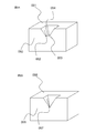
- the semiconductor substrate of the present invention has a plurality of dot markings formed on the surface thereof, each having an inverted frustum-shaped or inverted frustum-shaped recess, more preferably an inverted frustum-shaped recess.
- An inverted conical recess means a recess having a vertex at the bottom; an inverted frustum-shaped recess means a recess having a surface at the bottom.
- the semiconductor substrate of the present invention is preferably a silicon wafer, more preferably a silicon wafer having a crystal orientation (100).
- the thickness of the semiconductor substrate having dot markings is appropriately set according to the application, but when used as a semiconductor substrate of a solar cell, it is usually preferably in the range of 100 ⁇ m to 200 ⁇ m.
- a plurality of dot markings formed of recesses are formed on one semiconductor substrate.
- 16 ⁇ 16 dots or 18 ⁇ 18 dots are formed on the semiconductor substrate; a plurality of 16 ⁇ 16 dots or 18 ⁇ 18 dots may be formed on one semiconductor substrate.
- a two-dimensional code is configured. All of the dot markings constituting the two-dimensional code are preferably inverted frustum-shaped concave portions (see FIG. 2A) having a bottom surface.
- the dot marking can be formed at any position on the surface of the semiconductor substrate; however, the marking is easy to read, and the marking does not affect the quality of the semiconductor substrate.
- the dot marking position is set so that it does not disappear during the processing step. From these points, the dot marking is usually arranged at the peripheral portion of the semiconductor substrate surface, preferably at the corner portion.
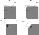
- FIG. 1AB shows a state in which a plurality of dot markings are formed at the corner of the semiconductor substrate.
- a two-dimensional code 005 called a data matrix composed of a plurality of dot markings is printed on the surface of a semiconductor substrate (single crystal silicon wafer 001).
- a two-dimensional code 010 called a data matrix composed of a plurality of dot markings is printed on the surface of a semiconductor substrate (single crystal silicon wafer 006).
- the two-dimensional codes 005 and 010 are each arranged in a rectangular area.
- the area of the rectangular region is preferably 0.25 to 9 mm 2 , for example, preferably about 1 mm 2 .
- markings of 16 ⁇ 16 dots or 18 ⁇ 18 dots are formed in a rectangular region.
- the sides of the rectangular area where the two-dimensional codes 005 and 010 are arranged are not parallel to the four sides of the semiconductor substrate (single crystal silicon wafers 001 and 006) but are inclined by 45 °. Further, a part of the corner of the semiconductor substrate (single crystal silicon wafer 006) is cut.
- the two-dimensional codes 005 and 010 are arranged in a region of the semiconductor substrate surface that does not contribute to power generation or has a low degree of contribution.
- the area of the region is preferably as small as possible. From this, it is preferable to form a plurality of dot markings in a rectangular region having sides parallel to the cut portion of the corner portion of the semiconductor substrate, as shown in FIG. 1B.
- the recesses that make up the dot marking are required to have high reading accuracy by the reading device and be as fine as possible.
- FIG. 2AB shows a perspective view of a dot marking made of a recess formed in a silicon wafer (050,055).
- FIG. 2A shows an example of dot marking composed of a concave truncated cone-shaped concave portion
- FIG. 2B shows an example of inverted pyramidal dot marking.
- a preferred dot marking is an inverted frustum-shaped recess as shown in FIG. 2A. This is because the reading accuracy of the reading device is high.
- an inverted conical recess means a recess having a vertex at the bottom; an inverted frustum-shaped recess means a recess having a surface at the bottom.
- the side surfaces of the recesses constituting the dot marking are tapered and tilted with respect to the substrate surface.
- the side surface of the recess has four or more trapezoidal tapered surfaces (single crystal silicon (111) surface 052) (FIG. 2A), or four or more triangular tapered surfaces (single crystal silicon (111) surface). 057) (FIG. 2B).
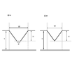
- FIG. 3AB shows a cross-sectional view of the concave portion constituting the dot marking.
- FIG. 3A shows an example of dot marking made of a reverse frustum-shaped concave portion
- FIG. 3B shows an example of a reverse frustum-shaped dot marking.
- the side surface (062,063) of the recess is inclined with respect to the substrate surface.
- the inclination angle 065 is typically in the range of 54 to 55 °, and the variation 066 is preferably ⁇ 10 °. Therefore, the inclination angle 065 is preferably in the range of 44 to 65 °.
- the reading accuracy by the optical reading device is improved by appropriately setting the tilt angle 065.
- an inclination angle 065 By assigning an inclination angle 065 to the inner surface of the concave portion constituting the dot marking, it becomes possible to distinguish the dot-shaped unprocessed portion and the dot-shaped processed portion on the wafer surface by making them a bright portion and a dark portion. .
- the inclination angle 065 is preferably 44 ° or more.
- the inclination angle 065 is excessively large, it is necessary to excessively increase the depth of the concave portion in order to make the opening diameter of the concave portion constituting the dot marking more than a certain value. In order to increase the depth of the recess excessively, the thickness of the semiconductor substrate needs to be excessively increased, which is not preferable. Therefore, the inclination angle 065 is preferably in the range of 44 to 65 °.
- the optical reading device for reading dot marking is distinguished by irradiating the dot marking with light from the upper part of the dot marking part by ring illumination and making the dot shape unprocessed part and dot shape processed part light and dark parts. To do. Depending on the diameter of the ring illumination, the illumination installation distance, and the illumination illuminance, the contrast of the light and dark portion differs.
- the selection and installation position of the ring illumination may be set according to the inclination angle 065 of the inner surface of the recess and the variation in the angle.
- FIG. 4AB shows a cross-sectional view of the concave portion constituting the dot marking.
- FIG. 4A is a cross-sectional view of dot marking composed of inverted frustum-shaped recesses;
- FIG. 4B is a cross-sectional view of dot marking consisting of inverted frustum-shaped recesses.
- the opening diameter (the diameter of the recess on the surface of the semiconductor substrate) W of the recesses constituting the dot marking is preferably in the range of 20 ⁇ m to 200 ⁇ m.
- the opening diameter W of the recess is preferably smaller than the thickness T of the semiconductor substrate.
- the depth H of the recessed part which comprises dot marking should just be smaller than the thickness T of the said semiconductor substrate, However, It is preferable that it is 20 micrometers or more. Further, the diameter w of the bottom surface of the recess is preferably 20 ⁇ m or less.
- the reading accuracy of the dot marking by the reading device can be improved. That is, the reflection and absorption of light during illumination irradiation of the optical reading device is stabilized, and as a result, the dot marking reading rate can be improved.
- the reading accuracy or reading rate is more likely to be higher with dot markings having inverted frustum-shaped recesses than with dot markings having inverted frustum-shaped recesses. Accordingly, it is preferable that the concave portions of all dot markings constituting the two-dimensional code have an inverted frustum shape.
- the opening diameter W, depth H and bottom surface diameter w of the recesses are adjusted by adjusting the opening diameter and depth of the recesses formed on the surface of the semiconductor substrate by laser irradiation, and adjusting the etching time. And can be adjusted.
- a typical data matrix and QR code registered trademark
- other character information and symbols formed using dots are described on the semiconductor substrate. be able to. In addition, these can be expressed in a very fine area.
- the information written on the semiconductor substrate includes, for example, information on production bases, information on production lines, information on the types of solar cells to be manufactured, information on production times, etc. It is.
- the semiconductor substrate which has the dot marking of this invention is the process of 1) preparing a semiconductor substrate, 2) The process of irradiating the surface of a semiconductor substrate with a laser, and forming several recessed part And 3) a step of performing wet etching on the substrate on which the recesses are formed.
- the prepared semiconductor substrate is preferably a single crystal silicon wafer, and is preferably a single crystal silicon wafer having a crystal orientation (100).
- the thickness is not particularly limited, and a semiconductor substrate having a desired thickness may be prepared in accordance with the set thickness of the semiconductor substrate included in the final device.
- a recess is formed by irradiating a laser on the surface of the semiconductor substrate.
- the concave portions may be formed using a green laser processing machine.
- the green laser is a laser that oscillates green light having a wavelength of about 532 nm.
- the semiconductor substrate in which the recesses are formed by laser irradiation is exposed to a plurality of etching processes and film forming processes. And the shape (depth, opening diameter, etc.) of a recessed part changes through an etching process or a film-forming process. Therefore, the diameter and depth of the recess formed by laser irradiation are adjusted so that the dot marking made of the recess after all the processes including a plurality of etching processes and film forming processes can be read.
- the shape of the recess formed by laser irradiation is, for example, a circle as shown in FIG. 5A, but is not particularly limited, and may be a rectangle such as a rectangle or a rectangle or another shape.
- FIGS. 5A to 5C Examples of the recesses 011 formed by laser irradiation are shown in FIGS. 5A to 5C.
- FIG. 5A is an SEM image from above the recess 011;
- FIG. 5BC is a diagram schematically showing a cross section of the recess 011 along the line AA in FIG. 5A.
- burrs (031, 033) are generated around the recesses 011.
- the inner surface of the recess 011 may be a “smooth curved surface” as shown in the sectional view of the recess in FIG. 5B; however, as shown in the sectional view of the recess in FIG. It may be a “curved surface including irregularities” and may have convex portions 034.
- FIG. 5D shows an image when the dot marking composed of the recesses 011 shown in FIG. 5A is read by an optical reading device.
- the left figure of FIG. 5D is a code photograph read by the reader; the right figure of FIG. 5D is a code figure to be read.
- the code photograph read by the optical reader is unclear and difficult to read.
- One reason for this is that there is a burr (031, 033, see FIG. 5BC) in the concave portion 011 or a “curved surface including a plurality of irregularities (see FIG. 5C)” on the inner surface of the concave portion. It is to diffusely reflect light.
- the shape of the concave portion 011 is optimized by wet etching the semiconductor substrate on which the concave portion 011 is formed by laser irradiation.
- the etchant for wet etching varies depending on the type of the semiconductor substrate, but in the case of a crystal orientation (100) silicon wafer, an alkali etchant is preferable.
- the semiconductor substrate on which the recesses 011 are formed is treated with an alkali etchant (for example, immersed in an alkali etchant) to remove burrs (031, 033) of the recesses 011 and to flatten the inner surface of the recesses 011.
- an alkali etchant for example, immersed in an alkali etchant
- Etching of a semiconductor substrate with an alkali etchant can be a process that is inevitably performed in a production process of a solar cell.
- a damaged layer processed altered layer
- an oxide layer of a commercially available silicon wafer is subjected to alkali wet etching.
- the shape of the recesses 011 formed by laser irradiation can be processed.
- the crystal orientation (100) silicon wafer is anisotropically etched by an alkali etchant.
- the plane of the crystal orientation (111) (052 in FIG. 2A, FIG. 2B057) is the plane of the crystal orientation (100) (051 or 053 in FIG. 2A, 056 in FIG. 2B) or the crystal orientation (221). It is easier to etch than the surface (054 in FIG. 2A). Therefore, the concave portion 011 formed by laser irradiation by alkali etching becomes a concave portion 014 shown in FIGS. 6A to 6C.
- FIG. 6A is an SEM image from above the recessed portion 014 after etching
- FIG. 6BC is a diagram schematically showing a cross section of the recessed portion 014 along the line BB in FIG. 6A.
- FIG. 6ABC there is no burr in the recess 014, and the inner surface (041,042) of the recess 014 is a flat tapered surface.
- a dot shape with conspicuous burrs and irregularities such as the concave part 011 (see FIG. 5) printed on the single crystal silicon wafer by a laser becomes like the concave part 014 (see FIG. 6) through the etching process.
- the dot shape has a flat inclined surface without burrs.
- FIG. 6D shows an image when the dot marking composed of the recesses 014 shown in FIG. 6A is read by an optical reading device.
- the left figure of FIG. 6D is a code photograph read by the reader; the right figure of FIG. 6D is a code figure to be read.
- the code photograph of the dot marking optical reading device including the recess 014 is clearer than the code photo of the dot marking optical reading device including the recess 011. .
- the burrs in the recesses formed by the laser irradiation are eliminated by wet etching, and the side surfaces of the distorted recesses are formed as flat inclined surfaces to form recesses having a desired shape.
- the variation in the shape of the concave portion is reduced, and the light reflection direction is also defined.
- the reading time of the code printed by the dot marking made of the concave portion is shortened, and the code reading rate is improved.
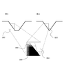
- the recess 014 is further processed by further alkali wet etching, which is inevitably performed in the production process of the solar cell. This is shown in FIG.
- the upper diagram in FIG. 7 shows the shape of the recess observed from above; the lower diagram in FIG.
- a recess 011 (see FIG. 5) formed by laser irradiation forms a recess 014 (see FIG. 6) through an initial alkali etching step.
- the shape of the recess 014 can be indicated by P1.
- the recesses 011 formed by laser irradiation such as the diameter and depth of the recesses 011
- the recesses may be indicated by any of P2 to P5.
- the shape of the formed recess 014 often changes in order from the P1 state to the P2, P3, P4, and P5 states by further alkaline wet etching.
- the order is P1 ⁇ P4 ⁇ P5.
- a transition occurs or a transition is made in the order of P1, P2, P3, and P5.
- both the opening and the bottom are octagonal.
- the side surface of the recess includes at least four trapezoidal flat tapered surfaces and a rectangular surface between the trapezoidal flat tapered surfaces.
- the side surface of the concave portion indicated by P1 may include other surfaces.
- P1-1 and P1-2 have side surfaces perpendicular to the substrate surface from the opening;
- P1-2 and P1-4 have side surfaces perpendicular to the substrate surface from the bottom surface.
- the opening shown in P2 in FIG. 7 has a quadrangular opening and an octagonal bottom.
- the shape of the opening is changed to become the recess indicated by P2. Except that the opening is square, it is the same as the recess shown in P1.
- the opening is a quadrangle, and the bottom is an octagon or a quadrangle.
- the side surface of the recess has four trapezoidal flat tapered surfaces. Unlike the side surface of the concave portion shown in P2, the concave portion shown in P3 does not have a rectangular surface between the trapezoidal flat tapered surfaces. Other points are the same as those of the concave portion indicated by P2.
- the opening shown in P4 of FIG. 7 has an octagonal shape and a vertex at the bottom.
- an opening part has a square shape and has a vertex in a bottom part. In this way, as the etching progresses, the surface at the bottom of the recess disappears.
- the inverted frustum-shaped concave portion having the bottom surface as shown by P1 to P3 has a higher reading accuracy by the reading device than the inverted frustum-shaped concave portion having the apex as shown by P4 to P5. Easy to increase.
- the shape of the recess changes every time the etching process is performed, and the depth of the recess changes after the film formation process. Therefore, the etching amount in each etching process and the film thickness in the film forming process are acquired in advance; and formed by laser irradiation so that a desired recess is formed in accordance with the data acquired in advance. Adjust the shape (opening diameter and depth) of the recess. Thereby, it can be ensured that the dot marking by the concave portion can be stably read until the final process.
- a single crystal silicon wafer for solar cells was prepared.
- the crystal orientation of the prepared single crystal silicon wafer was (100), and the wafer thickness was 180 ⁇ m.
- Green Laser Marker LP-G Series Panasonic Electric Works SUNX Co., Ltd., wavelength 532 nm
- a two-dimensional code called is printed.
- the aperture of the recess formed in the single crystal silicon wafer was targeted at 50 ⁇ m, and the depth of the recess was targeted at 60 ⁇ m.
- the shape of the recess formed by laser processing is shown in the SEM photograph of FIG. 5A.
- the data matrix code printed by the laser is arranged in a rectangular area of 1 mm ⁇ 1 mm.
- the number of dots (number of cells) was printed as 16 ⁇ 16.
- the position where the data matrix is printed is indicated by 005 in FIG. 1A or 010 in FIG. 1B.
- the single crystal silicon wafer on which the data matrix was printed with a laser was wet etched.
- the etchant was obtained by immersing a single crystal silicon wafer in an alkali-containing aqueous solution.
- the shape of the recess after wet etching is shown in the SEM photograph of FIG. 6A.
- the angle of the inner wall surface of the recess shown in FIG. 6A was about 54 to 55 °.
- the reading rate by an optical reader was measured for 100 wafers printed with data matrix codes consisting of recesses formed by laser processing and 100 wafers printed with data matrix codes by wet etching.
- the data matrix code was irradiated by ring illumination.
- the diameter of the ring illumination used was 20 mm to 50 mm wide.
- the installation distance of the ring illumination was 85 mm.
- the reading rate of the data matrix code printed only by laser processing was 30% to 50%, whereas the reading rate of the data matrix code printed by further wet etching was 99% or more. It was.
- the dot marking attached to the semiconductor substrate having the marking of the present invention can be stably read by the optical reading device. Moreover, the dot marking applied to the semiconductor substrate having the marking of the present invention can be applied within a very small area. Therefore, according to the semiconductor substrate having the marking of the present invention, manufacturing process management of a solar cell (for example, a silicon solar cell) having the semiconductor substrate becomes possible.
- a solar cell for example, a silicon solar cell
- information can be given to semiconductor substrates for various purposes.
- the present invention can be applied to the management of semiconductor wafers in a semiconductor process that conventionally prints character information.
Landscapes
- Physics & Mathematics (AREA)
- General Physics & Mathematics (AREA)
- Weting (AREA)
- Photovoltaic Devices (AREA)
- Laser Beam Processing (AREA)
- Chemical & Material Sciences (AREA)
- Chemical Kinetics & Catalysis (AREA)
- General Chemical & Material Sciences (AREA)
Abstract
Priority Applications (4)
| Application Number | Priority Date | Filing Date | Title |
|---|---|---|---|
| CN2012800160086A CN103477433A (zh) | 2011-06-22 | 2012-06-22 | 具有点标记的半导体基板及其制造方法 |
| JP2012541245A JP5124058B1 (ja) | 2011-06-22 | 2012-06-22 | ドットマーキングを有する半導体基板、およびその製造方法 |
| US13/703,728 US8860227B2 (en) | 2011-06-22 | 2012-06-22 | Semiconductor substrate having dot marks and method of manufacturing the same |
| EP20120775424 EP2560191A4 (fr) | 2011-06-22 | 2012-06-22 | Substrat semi-conducteur ayant des marquages de points, et son procédé de production |
Applications Claiming Priority (2)
| Application Number | Priority Date | Filing Date | Title |
|---|---|---|---|
| JP2011-138359 | 2011-06-22 | ||
| JP2011138359 | 2011-06-22 |
Publications (1)
| Publication Number | Publication Date |
|---|---|
| WO2012176473A1 true WO2012176473A1 (fr) | 2012-12-27 |
Family
ID=47422327
Family Applications (1)
| Application Number | Title | Priority Date | Filing Date |
|---|---|---|---|
| PCT/JP2012/004073 Ceased WO2012176473A1 (fr) | 2011-06-22 | 2012-06-22 | Substrat semi-conducteur ayant des marquages de points, et son procédé de production |
Country Status (5)
| Country | Link |
|---|---|
| US (1) | US8860227B2 (fr) |
| EP (1) | EP2560191A4 (fr) |
| JP (1) | JP5124058B1 (fr) |
| CN (1) | CN103477433A (fr) |
| WO (1) | WO2012176473A1 (fr) |
Cited By (4)
| Publication number | Priority date | Publication date | Assignee | Title |
|---|---|---|---|---|
| CN103794135A (zh) * | 2014-02-17 | 2014-05-14 | 立德高科(北京)数码科技有限责任公司 | 由点阵与二维码形成的标识及对其进行生成与识别的方法 |
| JP2015005549A (ja) * | 2013-06-19 | 2015-01-08 | パナソニック株式会社 | マーキングを有する太陽電池セルおよびその製造方法 |
| US10923606B2 (en) | 2016-10-26 | 2021-02-16 | Kaneka Corporation | Photoelectric conversion element |
| WO2024111178A1 (fr) * | 2022-11-22 | 2024-05-30 | 株式会社Sumco | Tranche de silicium avec marque laser et son procédé de production |
Families Citing this family (10)
| Publication number | Priority date | Publication date | Assignee | Title |
|---|---|---|---|---|
| CN103792715B (zh) * | 2014-01-27 | 2017-01-25 | 北京京东方显示技术有限公司 | 一种显示基板制造方法、系统及装置 |
| US9269035B2 (en) * | 2014-02-28 | 2016-02-23 | Electro Scientific Industries, Inc. | Modified two-dimensional codes, and laser systems and methods for producing such codes |
| KR20160038568A (ko) * | 2014-09-30 | 2016-04-07 | (주)포인트엔지니어링 | 복수의 곡면 캐비티를 포함하는 칩 기판 |
| US11088189B2 (en) | 2017-11-14 | 2021-08-10 | Taiwan Semiconductor Manufacturing Co., Ltd. | High light absorption structure for semiconductor image sensor |
| CN108538757B (zh) * | 2018-03-27 | 2020-12-01 | 韩华新能源(启东)有限公司 | 一种太阳能电池制程追溯方法 |
| JP7401284B2 (ja) * | 2019-12-12 | 2023-12-19 | 東京エレクトロン株式会社 | 基板処理装置 |
| JP7587570B2 (ja) * | 2020-03-26 | 2024-11-20 | デンカ株式会社 | セラミックス回路基板、放熱部材及びアルミニウム-ダイヤモンド系複合体 |
| CN116154013B (zh) * | 2021-11-19 | 2026-01-23 | 浙江晶科能源有限公司 | 一种光伏电池及光伏组件 |
| US12254366B2 (en) | 2021-11-29 | 2025-03-18 | General Electric Company | System to track hot-section flowpath components in assembled condition using high temperature material markers |
| CN115117022A (zh) | 2022-03-03 | 2022-09-27 | 晶科能源(海宁)有限公司 | 光伏电池及其形成方法、光伏组件 |
Citations (12)
| Publication number | Priority date | Publication date | Assignee | Title |
|---|---|---|---|---|
| JPH0593054A (ja) | 1991-10-02 | 1993-04-16 | Asahi Chem Ind Co Ltd | 熱可塑性合成樹脂成形品 |
| JPH05335197A (ja) | 1992-05-27 | 1993-12-17 | Oki Shisutetsuku Tokai:Kk | 半導体結晶基板の位置合わせ方法と合わせマーク形状 |
| JPH0684455A (ja) | 1992-07-15 | 1994-03-25 | Canon Inc | 微小ティップ、プローブユニット、及びこれらの製造方法、及びこれらを用いた走査型トンネル顕微鏡並びに情報処理装置 |
| JPH0980061A (ja) | 1995-09-14 | 1997-03-28 | Canon Inc | 微小探針の製造方法及びその製造用雌型基板、並びにその微小探針を有するプローブの製造方法とそのプローブ |
| JP2000223382A (ja) * | 1998-11-25 | 2000-08-11 | Komatsu Ltd | レ―ザビ―ムによる微小ドットマ―ク形態、そのマ―キング方法 |
| JP2002064214A (ja) | 2000-08-17 | 2002-02-28 | Honda Motor Co Ltd | 太陽電池の集電用電極およびその製造方法 |
| JP2004047776A (ja) | 2002-07-12 | 2004-02-12 | Honda Motor Co Ltd | 太陽電池セルおよびその製造方法 |
| JP2004095814A (ja) | 2002-08-30 | 2004-03-25 | Matsushita Electric Ind Co Ltd | 基板のマーキング方法とその装置 |
| WO2005069001A1 (fr) | 2003-09-25 | 2005-07-28 | Toyama Prefecture | Puce de reseau de micropuits et son procede de fabrication |
| US20060131424A1 (en) | 2003-08-22 | 2006-06-22 | Memscap | Article comprising an integrated marking tag and a mark-detection device |
| JP2006351620A (ja) * | 2005-06-13 | 2006-12-28 | Toshiba Corp | 半導体装置、半導体装置の製造方法および半導体装置の情報管理システム |
| JP2011023615A (ja) * | 2009-07-17 | 2011-02-03 | Panasonic Corp | 識別マーク |
Family Cites Families (11)
| Publication number | Priority date | Publication date | Assignee | Title |
|---|---|---|---|---|
| US5310674A (en) * | 1982-05-10 | 1994-05-10 | Bar-Ilan University | Apertured cell carrier |
| US4847183A (en) * | 1987-09-09 | 1989-07-11 | Hewlett-Packard Company | High contrast optical marking method for polished surfaces |
| JP2574984Y2 (ja) | 1992-05-22 | 1998-06-18 | シャープ株式会社 | 太陽電池セル |
| JPH0988061A (ja) | 1995-09-27 | 1997-03-31 | Mitsubishi Constr Co Ltd | 杭の支持力強化工法及びその装置 |
| US6774340B1 (en) | 1998-11-25 | 2004-08-10 | Komatsu Limited | Shape of microdot mark formed by laser beam and microdot marking method |
| WO2002003142A2 (fr) * | 2000-06-30 | 2002-01-10 | President And Fellows Of Harvard College | Procede et dispositif pour l'impression de microcontacts electriques |
| JP4071476B2 (ja) * | 2001-03-21 | 2008-04-02 | 株式会社東芝 | 半導体ウェーハ及び半導体ウェーハの製造方法 |
| US7169578B2 (en) * | 2001-07-27 | 2007-01-30 | Surface Logix, Inc. | Cell isolation and screening device and method of using same |
| JP4261274B2 (ja) | 2003-07-30 | 2009-04-30 | Sumco Techxiv株式会社 | レーザマークがされた円板状部材のエッチング方法及びその装置 |
| JP4669270B2 (ja) * | 2004-12-02 | 2011-04-13 | 富士通株式会社 | Rfidタグおよびその製造方法 |
| JP2011029355A (ja) * | 2009-07-24 | 2011-02-10 | Sumco Corp | レーザマーク付き半導体ウェーハの製造方法 |
-
2012
- 2012-06-22 WO PCT/JP2012/004073 patent/WO2012176473A1/fr not_active Ceased
- 2012-06-22 JP JP2012541245A patent/JP5124058B1/ja active Active
- 2012-06-22 EP EP20120775424 patent/EP2560191A4/fr not_active Ceased
- 2012-06-22 CN CN2012800160086A patent/CN103477433A/zh active Pending
- 2012-06-22 US US13/703,728 patent/US8860227B2/en active Active
Patent Citations (15)
| Publication number | Priority date | Publication date | Assignee | Title |
|---|---|---|---|---|
| JPH0593054A (ja) | 1991-10-02 | 1993-04-16 | Asahi Chem Ind Co Ltd | 熱可塑性合成樹脂成形品 |
| JPH05335197A (ja) | 1992-05-27 | 1993-12-17 | Oki Shisutetsuku Tokai:Kk | 半導体結晶基板の位置合わせ方法と合わせマーク形状 |
| JPH0684455A (ja) | 1992-07-15 | 1994-03-25 | Canon Inc | 微小ティップ、プローブユニット、及びこれらの製造方法、及びこれらを用いた走査型トンネル顕微鏡並びに情報処理装置 |
| US5546375A (en) | 1992-07-15 | 1996-08-13 | Canon Kabushiki Kaisha | Method of manufacturing a tip for scanning tunneling microscope using peeling layer |
| JPH0980061A (ja) | 1995-09-14 | 1997-03-28 | Canon Inc | 微小探針の製造方法及びその製造用雌型基板、並びにその微小探針を有するプローブの製造方法とそのプローブ |
| US5866021A (en) | 1995-09-14 | 1999-02-02 | Canon Kabushiki Kaisha | Method of manufacturing micro-tip and female mold substrate therefor, and method of manufacturing probe with micro-tip and the probe |
| JP2000223382A (ja) * | 1998-11-25 | 2000-08-11 | Komatsu Ltd | レ―ザビ―ムによる微小ドットマ―ク形態、そのマ―キング方法 |
| JP2002064214A (ja) | 2000-08-17 | 2002-02-28 | Honda Motor Co Ltd | 太陽電池の集電用電極およびその製造方法 |
| JP2004047776A (ja) | 2002-07-12 | 2004-02-12 | Honda Motor Co Ltd | 太陽電池セルおよびその製造方法 |
| JP2004095814A (ja) | 2002-08-30 | 2004-03-25 | Matsushita Electric Ind Co Ltd | 基板のマーキング方法とその装置 |
| US20060131424A1 (en) | 2003-08-22 | 2006-06-22 | Memscap | Article comprising an integrated marking tag and a mark-detection device |
| WO2005069001A1 (fr) | 2003-09-25 | 2005-07-28 | Toyama Prefecture | Puce de reseau de micropuits et son procede de fabrication |
| US20080014631A1 (en) | 2003-09-25 | 2008-01-17 | Sachiko Kondo | Microwell Array Chip and Its Manufacturing Method |
| JP2006351620A (ja) * | 2005-06-13 | 2006-12-28 | Toshiba Corp | 半導体装置、半導体装置の製造方法および半導体装置の情報管理システム |
| JP2011023615A (ja) * | 2009-07-17 | 2011-02-03 | Panasonic Corp | 識別マーク |
Non-Patent Citations (1)
| Title |
|---|
| See also references of EP2560191A4 |
Cited By (5)
| Publication number | Priority date | Publication date | Assignee | Title |
|---|---|---|---|---|
| JP2015005549A (ja) * | 2013-06-19 | 2015-01-08 | パナソニック株式会社 | マーキングを有する太陽電池セルおよびその製造方法 |
| CN103794135A (zh) * | 2014-02-17 | 2014-05-14 | 立德高科(北京)数码科技有限责任公司 | 由点阵与二维码形成的标识及对其进行生成与识别的方法 |
| US10923606B2 (en) | 2016-10-26 | 2021-02-16 | Kaneka Corporation | Photoelectric conversion element |
| WO2024111178A1 (fr) * | 2022-11-22 | 2024-05-30 | 株式会社Sumco | Tranche de silicium avec marque laser et son procédé de production |
| JP7771932B2 (ja) | 2022-11-22 | 2025-11-18 | 株式会社Sumco | レーザーマーク付きシリコンウェーハ及びその製造方法 |
Also Published As
| Publication number | Publication date |
|---|---|
| EP2560191A1 (fr) | 2013-02-20 |
| CN103477433A (zh) | 2013-12-25 |
| JPWO2012176473A1 (ja) | 2015-02-23 |
| EP2560191A4 (fr) | 2013-09-25 |
| JP5124058B1 (ja) | 2013-01-23 |
| US20130193560A1 (en) | 2013-08-01 |
| US8860227B2 (en) | 2014-10-14 |
Similar Documents
| Publication | Publication Date | Title |
|---|---|---|
| JP5124058B1 (ja) | ドットマーキングを有する半導体基板、およびその製造方法 | |
| CN101395724B (zh) | 太阳能电池标记方法和太阳能电池 | |
| TWI531086B (zh) | An optical substrate, a semiconductor light-emitting element, and a semiconductor light-emitting element | |
| EP1733438B1 (fr) | Modelisation au laser de dispositifs electroluminescents et dispositifs electroluminescents ainsi obtenus | |
| CN104425219A (zh) | 制造金属掩模的方法及使用该方法形成的金属掩模 | |
| CN109755220B (zh) | 发光装置及其制作方法 | |
| JP3242632B2 (ja) | レーザビームによる微小ドットマーク形態、そのマーキング方法 | |
| CN101877330A (zh) | 具有周期结构的蓝宝石基板 | |
| TW201244158A (en) | A method to fabrication an epitaxial substrate, a light emitting diode and the method to fabrication said light emitting diode | |
| US20110042711A1 (en) | Iii-nitride semiconductor light emitting device and method for fabricating the same | |
| CN102893409A (zh) | 光电动势装置的制造方法以及光电动势装置的制造装置 | |
| JP2001118757A (ja) | 微小ドットマークを有する半導体基材 | |
| WO2012013214A2 (fr) | Procédé de marquage d'une photopile, et photopile | |
| JP2001101337A (ja) | ドットマークの読取り装置と読取り方法 | |
| JP2011023615A (ja) | 識別マーク | |
| KR20250040719A (ko) | 레이저 마크 부착 실리콘 웨이퍼 및 그의 제조 방법 | |
| CN118039734A (zh) | 隧穿氧化层钝化接触电池加工方法和激光设备 | |
| JP2011131453A (ja) | 光学素子製造用ナノインプリントモールドの製造方法 | |
| CN113745376B (zh) | 发光芯片处理方法、发光芯片组件、显示装置及发光装置 | |
| JP2008216610A (ja) | レーザ加工用光学部品の製法 | |
| WO2011052395A1 (fr) | Tranche épitaxiale, procédé de fabrication d'une tranche épitaxiale, tranche d'éléments luminescents, procédé de fabrication d'une tranche d'éléments luminescents et élément luminescent | |
| US8900801B2 (en) | Method for producing a LED device | |
| KR20010022516A (ko) | 웨이퍼 마킹 방법 | |
| KR100857939B1 (ko) | 레이저 다이오드 제조를 위한 웨이퍼 절단 방법 및 이를위한 웨이퍼 구조 | |
| CN108011001A (zh) | 具有羽化表面的堆叠式图形化led衬底及led器件 |
Legal Events
| Date | Code | Title | Description |
|---|---|---|---|
| ENP | Entry into the national phase |
Ref document number: 2012541245 Country of ref document: JP Kind code of ref document: A |
|
| WWE | Wipo information: entry into national phase |
Ref document number: 2012775424 Country of ref document: EP |
|
| WWE | Wipo information: entry into national phase |
Ref document number: 13703728 Country of ref document: US |
|
| 121 | Ep: the epo has been informed by wipo that ep was designated in this application |
Ref document number: 12775424 Country of ref document: EP Kind code of ref document: A1 |
|
| NENP | Non-entry into the national phase |
Ref country code: DE |