WO2013084294A1 - Dispositif de mesure de quantité dynamique - Google Patents
Dispositif de mesure de quantité dynamique Download PDFInfo
- Publication number
- WO2013084294A1 WO2013084294A1 PCT/JP2011/078183 JP2011078183W WO2013084294A1 WO 2013084294 A1 WO2013084294 A1 WO 2013084294A1 JP 2011078183 W JP2011078183 W JP 2011078183W WO 2013084294 A1 WO2013084294 A1 WO 2013084294A1
- Authority
- WO
- WIPO (PCT)
- Prior art keywords
- region
- quantity measuring
- semiconductor chip
- mechanical quantity
- strain
- Prior art date
- Legal status (The legal status is an assumption and is not a legal conclusion. Google has not performed a legal analysis and makes no representation as to the accuracy of the status listed.)
- Ceased
Links
Images










Classifications
-
- G—PHYSICS
- G01—MEASURING; TESTING
- G01B—MEASURING LENGTH, THICKNESS OR SIMILAR LINEAR DIMENSIONS; MEASURING ANGLES; MEASURING AREAS; MEASURING IRREGULARITIES OF SURFACES OR CONTOURS
- G01B7/00—Measuring arrangements characterised by the use of electric or magnetic techniques
- G01B7/16—Measuring arrangements characterised by the use of electric or magnetic techniques for measuring the deformation in a solid, e.g. by resistance strain gauge
- G01B7/18—Measuring arrangements characterised by the use of electric or magnetic techniques for measuring the deformation in a solid, e.g. by resistance strain gauge using change in resistance
-
- G—PHYSICS
- G01—MEASURING; TESTING
- G01B—MEASURING LENGTH, THICKNESS OR SIMILAR LINEAR DIMENSIONS; MEASURING ANGLES; MEASURING AREAS; MEASURING IRREGULARITIES OF SURFACES OR CONTOURS
- G01B7/00—Measuring arrangements characterised by the use of electric or magnetic techniques
- G01B7/16—Measuring arrangements characterised by the use of electric or magnetic techniques for measuring the deformation in a solid, e.g. by resistance strain gauge
-
- G—PHYSICS
- G01—MEASURING; TESTING
- G01L—MEASURING FORCE, STRESS, TORQUE, WORK, MECHANICAL POWER, MECHANICAL EFFICIENCY, OR FLUID PRESSURE
- G01L1/00—Measuring force or stress, in general
- G01L1/18—Measuring force or stress, in general using properties of piezo-resistive materials, i.e. materials of which the ohmic resistance varies according to changes in magnitude or direction of force applied to the material
Definitions
- the present invention relates to a mechanical quantity measuring apparatus, and more particularly to a technique effective when applied to a mechanical quantity measuring apparatus using a semiconductor strain sensor capable of measuring strain and stress of a structure.
- Patent Document 1 describes a strain detection sensor in which a sensor chip (strain detection element) is bonded to a glass base using low-melting glass.
- Patent Document 2 discloses a pressure sensor device for measuring the pressure of a fluid such as oil, on a convex portion of a metal member having a through hole, through a glass pedestal. A pressure sensor device having a structure in which a pressure sensor chip is mounted is described.
- a strain gauge is a structure in which a lead wire is provided by forming a wiring pattern of a Cu-Ni alloy or Ni-Cr alloy metal thin film on a polyimide or epoxy resin film. Adhere with and use. The amount of strain can be calculated from the change in resistance value resulting from the deformation of the metal thin film.
- a semiconductor strain sensor has a resistance change rate with respect to strain as large as several tens of times that of a strain gauge using a metal thin film, and can measure a minute strain.
- an external amplifier for amplifying the obtained electric signal is required. Since the semiconductor strain sensor has a large resistance change, the obtained electrical signal can be used without using an external amplifier, and it is also possible to build an amplifier circuit on the semiconductor chip of the semiconductor strain sensor. It is expected that the convenience of use and usage will be greatly expanded.
- the semiconductor strain sensor when the semiconductor strain sensor is attached to the object to be measured and the strain is measured, when the amount of strain of the object to be measured increases, there is a problem that the semiconductor chip itself constituting the semiconductor strain sensor is destroyed.
- the range of the strain amount that can be measured by the semiconductor strain sensor is regulated by the breaking strength of the semiconductor chip.
- the measurable range of a semiconductor strain sensor using a silicon substrate is limited to a range in which the silicon substrate does not break, and in order to measure stably, the measurable strain range is 1000 ⁇ (hereinafter referred to as strain amount).
- strain amount 1000 ⁇ (hereinafter referred to as strain amount).
- the inventor of the present application examined a method for expanding the range of the strain amount that can be measured by the semiconductor strain sensor.
- the inventor of the present application examined a configuration in which another member (hereinafter referred to as a pedestal) is bonded and fixed between the semiconductor strain sensor and the object to be measured, and the strain is transmitted to the semiconductor strain sensor through the pedestal.
- a semiconductor strain sensor was fixed on a pedestal and a modular mechanical quantity measuring device (sensor module) was examined.
- the strain generated in the object to be measured is transmitted to the semiconductor strain sensor via the pedestal, so that the amount of strain transmitted to the semiconductor strain sensor can be reduced by increasing the rigidity of the pedestal.
- the semiconductor strain sensor can measure a minute strain as described above, a small amount of strain transmitted to the semiconductor strain sensor via the pedestal is measured, and the measured object is measured based on the measurement result. The amount of strain generated can be calculated. That is, since the upper limit of the measurable strain amount is increased, the measurable strain amount range of the semiconductor strain sensor can be expanded.
- the present invention has been made in view of the above problems, and an object thereof is to provide a technique for improving the connection reliability between the mechanical quantity measuring device and the object to be measured.
- Another object of the present invention is to provide a technique for expanding the measurable range of the mechanical quantity measuring device.
- the present application includes a plurality of means for solving the above-described problems.
- An example of the means is as follows.
- a mechanical quantity measuring device includes a semiconductor chip in which a plurality of piezoresistive elements are formed on a surface of a semiconductor substrate, and a lead-out wiring portion electrically connected to the plurality of electrodes of the semiconductor chip. And a plate material bonded to the back surface of the semiconductor chip.
- the plate member includes a first region facing the back surface of the semiconductor chip, and a second region disposed on both sides of the first region, and the thickness of the plate member in the first region is determined. The thickness is larger than the thickness of the second region.
- connection reliability between the mechanical quantity measuring device and the object to be measured can be improved.
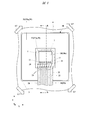
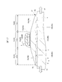
- FIG. 1 is an enlarged plan view showing a state in which a mechanical quantity measuring device according to an embodiment of the present invention is bonded and fixed on an object to be measured.
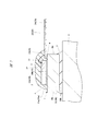
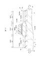
- FIG. 2 is an enlarged sectional view taken along line AA in FIG.
- FIG. 3 is an enlarged cross-sectional view along the line BB in FIG. 1.
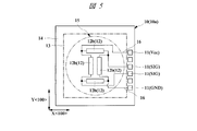
- FIG. 4 is a plan view schematically showing a configuration on the surface side of the semiconductor chip shown in FIGS. 1 to 3;
- FIG. 5 is a plan view schematically showing a configuration on the front surface side of a semiconductor chip which is a modified example with respect to FIG. 4. It is explanatory drawing which shows the relationship between the thickness of the board
- FIG. 9 is an enlarged sectional view taken along line BB in FIG.
- FIG. 9 is an expanded sectional view which shows the state by which the mechanical quantity measuring device which is a modification with respect to FIG. 2 was adhesive-fixed on the to-be-measured object.
- FIG. 9 shows the state by which the mechanical quantity measuring device which is a modification with respect to FIG.
- FIG. 10 was adhesive-fixed on the to-be-measured object. It is an expanded sectional view which shows the state by which the mechanical quantity measuring device which is another modification with respect to FIG. 2 was adhere
- FIG. 5 is a plan view schematically showing a configuration on the front surface side of a semiconductor chip which is a modified example with respect to FIG. 4.
- FIG. 6 is a plan view schematically showing a configuration on the front surface side of a semiconductor chip which is a modified example with respect to FIG. 5.
- FIG. 5 is a plan view schematically showing a configuration on the front surface side of a semiconductor chip which is a modified example with respect to FIG. 4.
- FIG. 6 is a plan view schematically showing a configuration on the front surface side of a semiconductor chip which is a modified example with respect to
- FIG. 16 is an enlarged plan view showing a mechanical quantity measuring device in which the semiconductor chip shown in FIG. 14 or FIG. 15 is mounted on the plate shown in FIG.
- FIG. 2 is a perspective plan view showing a state in which a mechanical quantity measuring device which is a comparative example with respect to FIG. 1 is bonded and fixed on an object to be measured.
- FIG. 18 is a cross-sectional view taken along line AA of FIG.
- constituent elements are not necessarily indispensable except for the case where they are clearly indicated and the case where they are clearly considered to be indispensable in principle.
- constituent elements and the like when “consisting of A”, “consisting of A”, “having A”, and “including A” are specifically indicated that only those elements are included. It goes without saying that other elements are not excluded except in the case of such cases.
- the shapes, positional relationships, etc. of the components, etc. when referring to the shapes, positional relationships, etc. of the components, etc., the shapes are substantially the same unless otherwise specified, or otherwise apparent in principle. And the like are included. The same applies to the above numerical values and ranges.
- hatching or the like may be omitted even in a cross section when it becomes complicated or when it is clearly distinguished from a gap.
- the contour line of the background may be omitted even if the hole is planarly closed.
- it may be hatched to clearly indicate that it is not a void.
- FIG. 1 is a perspective plan view showing a state in which the mechanical quantity measuring device according to the present embodiment is bonded and fixed on an object to be measured.
- 2 is a cross-sectional view taken along line AA in FIG. 1
- FIG. 3 is a cross-sectional view taken along line BB in FIG.
- FIG. 1 in order to show the internal structure of the sealing body 2, the outline of the sealing body 2 is indicated by a two-dot chain line, and the internal structure that has passed through the sealing body 2 is illustrated.
- 4 is a plan view schematically showing the configuration of the front surface side of the semiconductor chip shown in FIGS. 1 to 3
- FIG. 5 is a schematic diagram of the configuration of the front surface side of the semiconductor chip which is a modification to FIG. FIG.
- a sensor module 1 that is a mechanical quantity measuring device according to the present embodiment is electrically connected to a semiconductor chip (sensor chip) 10 that is a semiconductor strain sensor, and the semiconductor chip 10.
- a wiring part (lead wiring part, flexible wiring board) 20, a plate material (pedestal) 30 on which the semiconductor chip 10 is mounted via the bonding material 5, and a sealing body (resin body) 2 for sealing the semiconductor chip 10 have.
- FIG. 1 A wiring part (lead wiring part, flexible wiring board) 20
- a sealing body (resin body) 2 for sealing the semiconductor chip 10 have.
- the sensor module 1 is configured such that the lower surface (mounting surface) 30 b side of the plate member 30 is bonded and fixed to the measurement object 4 via an adhesive layer 3 made of resin, for example, and the strain applied to the measurement object 4 Is transmitted to the semiconductor chip 10 via the plate member 30, and the strain transmitted to the semiconductor chip 10 is measured.
- an example of measuring a strain (tensile strain) applied along the lower surface (mounting surface) 30 b (see FIG. 2) of the plate member 30 Will be explained.
- the semiconductor chip 10 includes a front surface (main surface) 10a and a back surface (main surface) 10b located on the opposite side of the front surface 10a as shown in FIG.
- a metal film 17 is formed on the back surface 10 b of the semiconductor chip 10, and the back surface 10 b is covered with the metal film 17.
- the metal film 17 is composed of a laminated film (metal laminated film) in which chromium, nickel, gold (Cr, Ni, Au) are sequentially laminated from the semiconductor substrate side, for example, and can be formed by, for example, sputtering.
- the bonding strength with the metal bonding material 5 such as solder can be improved.
- the front surface 10a and the back surface 10b each form a quadrilateral ((quadrangle), and in the example shown in FIGS. 4 and 5, for example, each side has a length of about 2 mm to 3 mm.
- the semiconductor chip 10 includes a plurality of resistance elements 12 formed in a sensor region 13 located at the center on the surface 10a side, and the semiconductor chip 10 includes a sensor region (on the surface 10a side)
- a plurality of electrodes (pads, electrode pads) 11 that are formed in the input / output circuit region 14 located on the peripheral side of the core region 13 and electrically connected to the plurality of resistance elements (piezoresistive elements) 12 are provided.
- the plurality of resistance elements 12 are constituted by impurity diffusion regions in which, for example, an element formation surface of a silicon substrate having a (100) plane is doped and diffused.
- a detection circuit (strain detection circuit) 15 is provided that electrically connects four resistance elements 12 to form a Wheatstone bridge circuit and measures a resistance change of the resistance element 12 due to the piezoresistance effect to detect strain.
- the detection circuit 15 is connected to a plurality of electrodes 11 via a plurality of wirings 16.
- the plurality of electrodes 11 serve as input / output terminals of the semiconductor chip 10, for example, a power supply potential to the semiconductor chip 10.
- a terminal Vcc that supplies (first power supply potential), a terminal GND that supplies a reference potential (second power supply potential), and a terminal SIG that outputs a detection signal are included.
- the layout of the plurality of resistance elements 12 constituting the detection circuit 15 is not limited to the mode shown in FIG. 4 and FIG. 5, but the following configuration is adopted in the present embodiment. That is, when the semiconductor substrate (for example, a silicon substrate made of silicon (Si)) included in the semiconductor chip 10 is a single crystal (silicon single crystal), the extending direction (longitudinal direction) of the plurality of resistance elements 12 constituting the detection circuit 15 ) Coincides with the ⁇ 110> direction or ⁇ 100> direction of a semiconductor substrate having a (100) plane. For example, in the example shown in FIG.
- the semiconductor substrate (silicon substrate) included in the semiconductor chip 10 has a crystal orientation in the ⁇ 110> direction of the silicon single crystal (the X direction and the Y direction orthogonal to the X direction in FIG. 4).
- Four p-type diffusion regions regions doped with impurities whose conductivity type is p-type) are formed so that a current flows along.
- four resistance elements 12 a are formed by doping p-type impurities at four locations so as to extend along the crystal orientation in the ⁇ 110> direction of the silicon single crystal of the silicon substrate. .
- the semiconductor substrate (silicon substrate) included in the semiconductor chip 10 has a crystal orientation in the ⁇ 100> direction of the silicon single crystal (the X direction and the Y direction orthogonal to the X direction in FIG. 4).
- Four p-type diffusion regions regions doped with impurities whose conductivity type is p-type) are formed so that a current flows along.
- four resistance elements 12 b are formed by doping n-type impurities at four locations so as to extend along the crystal orientation in the ⁇ 100> direction of the silicon single crystal of the silicon substrate. .
- the chip 10 can output, for example, the difference between the strain in the X direction and the strain in the Y direction shown in FIGS. 4 and 5.
- the difference between the strain in the X direction and the strain in the Y direction can be output as a potential difference from the terminal SIG shown in FIGS.
- the measurement method that outputs the difference between the strain in the X direction and the strain in the Y direction is advantageous from the viewpoint of reducing the influence of the thermal strain applied to the semiconductor chip 10. That is, as shown in FIG.
- the semiconductor chip 10 is fixed on the object to be measured 4 via a plurality of members (in the case of FIG. 2, the adhesive layer 3, the plate material 30, and the bonding material 5).
- a plurality of members in the case of FIG. 2, the adhesive layer 3, the plate material 30, and the bonding material 5.
- thermal strain due to the difference in linear expansion coefficient of each member occurs. Since this thermal strain is a noise component different from the strain to be measured, it is preferable to reduce the influence of thermal strain.
- FIGS. 4 and 5 when the planar shape of the semiconductor chip 10 is a square, the influence of thermal strain is approximately the same in the X direction and the Y direction.
- the strain amount due to the thermal strain is canceled, and the strain to be measured. Can be selectively detected. That is, if the semiconductor chip 10 is used, the influence of thermal strain can be reduced, so that variation in strain value due to changes in environmental temperature can be reduced.
- each member such as the resistance element 12, the wiring 16, or the electrode 11 constituting the semiconductor chip 10 can be formed by applying a known semiconductor device manufacturing technique, the elements and wirings can be easily miniaturized. It is. Moreover, manufacturing efficiency can be improved and manufacturing cost can be reduced.
- the plate member 30 for fixing the semiconductor chip 10 includes an upper surface (chip mounting surface) 30a, a lower surface (mounting surface) 30b located on the opposite side of the upper surface 30a, and between the upper surface 30a and the lower surface. A side surface 30c is provided.
- the plate member 30 has a function of relaxing stress transmitted from the device under test 4 to the semiconductor chip 10 (a strain amount of the semiconductor chip 10) and preventing the semiconductor chip 10 from being broken.
- the constituent material of the plate member 30 is not particularly limited, since it is preferable to use a metal bonding material such as solder as the bonding material 5 as will be described later, at least a chip from the viewpoint of improving the connection reliability with the bonding material 5.
- the upper surface 31a serving as a mounting surface is preferably made of metal. Moreover, it is preferable to comprise the whole board
- the plate member 30 has a region (chip mounting region) 31 on which the semiconductor chip 10 is mounted (facing the back surface 10 b of the semiconductor chip 10), and a region disposed on both sides of the region 31. 32, and the upper surface (chip mounting surface) 31a of the region 31 is disposed at a position higher than the upper surface 32a of the region 32.
- the lower surface 30b is arranged at the same height in both the regions 31 and 32 and is flattened. In other words, between the region 31 and the region 32, there is a side surface 31c continuous with the upper surface 31a of the region 31, and the region 31 protrudes upward (on the semiconductor chip 10 side).
- the thickness of the plate 30 in the region 31 is larger than the thickness of the region 32 (distance from the lower surface 30b to the upper surface 32a).
- the region 32 has the side surface 30 c of the plate member 30, and the thickness of the region 32 on the side surface 30 c is smaller than the thickness of the region 31.
- a bonding material 5 for bonding and fixing the semiconductor chip 10 and the plate material 30 is disposed between the semiconductor chip 10 and the plate material 30.
- the bonding material 5 is disposed so as to cover the entire back surface 10b of the semiconductor chip 10 and a part of the side surface (a part on the back surface 10b side). In other words, the peripheral edge of the bonding material 5 extends to the outside of the side surface of the semiconductor chip 10 to form a fillet.
- the bonding material 5 is not limited to a metal material, and for example, a resin adhesive such as a thermosetting resin can be used.
- the bonding material 5 is preferably made of a metal material.
- the sensor module 1 is a strain measuring device that transmits the strain generated in the DUT 4 as described above to the semiconductor chip 10 via the plate member 30 and measures the strain transmitted to the semiconductor chip 10.
- the strain generated in the DUT 4 is relaxed (reduced) by the plate 30 before being transmitted to the semiconductor chip 10.
- the degree of relaxation varies depending on the rigidity of the plate member 30, but in the present embodiment, the degree of relaxation is relaxed to such an extent that at least strain (for example, 1000 ⁇ or less) within a range in which the semiconductor chip 10 is not broken occurs.
- the amount of strain is smaller at the bonding interface between the semiconductor chip 10 and the plate material 30 than at the bonding interface between the DUT 4 and the plate material 30.
- the bonding material 5 for bonding and fixing the semiconductor chip 10 and the plate material 30 is made of resin
- the resin component in the adhesive relaxes the stress in a strained state, and the adhesive and the semiconductor chip 10 are deformed. The state changes.
- the measurement accuracy of the semiconductor chip 10 (the accuracy of the measurement result with respect to the strain generated in the DUT 4) is lowered.
- a metal material such as solder is used as the bonding material 5
- the influence on the deformation state is reduced. That is, by forming the bonding material 5 from a metal material such as solder, the measurement accuracy of the semiconductor chip 10 (accuracy of the measurement result with respect to the strain generated in the device under test 4) is improved as compared with the case of forming the bonding material 5 from resin. Can be made. Further, from the viewpoint of efficiently performing the process of fixing the semiconductor chip 10 on the plate member 30, it is particularly preferable that the bonding material 5 is made of solder. However, when the bonding material 5 made of solder is used, depending on the environmental temperature. It is conceivable that the bonding material 5 softens and relieves stress. Therefore, it is preferable to use a material having a high melting point of the bonding material.
- a wiring portion 20 including a plurality of wirings 22 electrically connected to the plurality of electrodes 11 of the semiconductor chip 10 is fixed to the upper surface 30 a of the plate member 30.
- the wiring part 20 is a so-called flexible wiring board in which the wiring part 20, which is a plurality of metal patterns, is sealed in the resin film 24, and a plurality of wirings are formed in an opening provided in a part of the resin film 24.
- Each part of 22 is exposed, and this exposed part constitutes a plurality of terminals 23.
- the plurality of electrodes 11 of the semiconductor chip 10 and the plurality of terminals 23 of the wiring portion 20 are electrically connected via a plurality of wires (conductive members) 21. .
- a part of the wiring portion 20 is bonded and fixed via an adhesive 6 on the upper surface 31 a of the region 31 that is a chip mounting region.
- the wire 21 is, for example, a gold wire (Au wire) having a wire diameter of about 10 ⁇ m to 200 ⁇ m, and is sealed by the sealing body 2.
- Au wire gold wire
- one end of the wiring section 20 is fixed to the plate member 30 as shown in FIG.
- the flexible wiring board portion is described as the wiring portion 20 and is distinguished from the wires 21.
- the wiring portion 20 including a plurality of wires 21 can also be regarded as the wiring portion 20.
- the wiring section 20 is not limited to the mode shown in FIGS. 1 to 3 as long as it can transmit input / output current between the semiconductor chip 10 and an external device (not shown).
- the sensor module 1 is bonded and fixed to the object to be measured 4 via the adhesive layer 3.
- the measured object 4, the adhesive layer 3, and the plate material 30 are laminated and bonded in this order so that the lower surface 30 b that is the mounting surface of the plate material 30 faces the sensor mounting surface (front surface, upper surface) of the measured object 4.
- the adhesive layer 3 is disposed so as to cover the entire lower surface 30b of the plate 30 and a part of the side surface 30c (a part on the lower surface 30b side). In other words, the peripheral edge portion of the adhesive layer 3 extends to the outside of the side surface 30c of the plate member 30 to form a fillet.
- the constituent material of the adhesive layer 3 is not particularly limited, it is preferable to use a resin adhesive such as a thermosetting resin from the viewpoint of easy attachment to the measurement object 4.
- a resin adhesive such as a thermosetting resin
- an adhesive generally used for example, a two-component or one-component epoxy resin is used.
- the adhesive layer 3 is formed using the same.
- an adhesive is applied to the lower surface 30b of the plate member 30, and the sensor module 1 is pressed and pasted to the object to be measured 4 and heated to the curing temperature. It can be fixed by heat curing.
- the adhesive layer 3 relieves stress in a strained state.
- stress relaxation by the adhesive layer 3 is particularly large at the peripheral edge of the adhesive layer 3. Accordingly, in the vicinity of the central portion where the semiconductor chip 10 is mounted, the influence of stress relaxation is small, so the influence on the strain state of the semiconductor chip 10 is small. That is, even when the bonding layer 3 disposed on the DUT 4 and the plate 30 is made of resin (including a case where a plurality of metal particles are mixed in the resin), the measurement accuracy of the semiconductor chip 10 is reduced. The impact is small.
- FIG. 6 is an explanatory diagram showing the relationship between the thickness of the plate material on which the semiconductor chip is mounted and the amount of strain generated in the semiconductor chip.
- FIG. 7 is an explanatory diagram showing the relationship between the thickness of the plate material on which the semiconductor chip is mounted and the strain generated at the end of the adhesive layer that bonds and fixes the plate material.
- FIG. 17 is a perspective plan view showing a state in which a mechanical quantity measuring device, which is a comparative example with respect to FIG. 1, is bonded and fixed on an object to be measured.
- FIG. 18 is a sectional view taken along line AA in FIG.
- FIG. 6 shows the relationship between the thickness of the plate material on which the semiconductor chip is mounted and the amount of strain generated in the semiconductor chip by a finite element method (FEM) analysis.
- FEM finite element method
- FIG. 7 shows the strain value (strain amount) generated at the end of the adhesive layer 3 (just below the peripheral edge of the region 32) under the same conditions as in FIG. 6, with the thickness of the plate material as a parameter.
- the sensor module H1 shown in FIGS. 17 and 18 is different in that the plate member H30 does not include the region 32 (thin plate region) like the plate member 30 shown in FIGS. The other points are the same as those of the sensor module 1 shown in FIGS.
- the DUT 4 and the plate material were made of duralumin, and the bonding material 5 was analyzed as high temperature solder.
- the semiconductor chip 10 is fixed on the upper surface 30a of the plate 30 via the bonding material 5, and is bonded and fixed to the object 4 to be measured via the adhesive layer 3.
- a strain value strain amount
- the amount of strain generated in the semiconductor chip 10 is reduced by about 25% with respect to the strain (1000 ⁇ ) applied to the DUT 4 when the thickness of the plate is at least 0.5 mm.
- the amount of strain generated in the semiconductor chip 10 further decreases. For example, when the plate thickness is 1 mm, it may be reduced by about 40%, and when the plate thickness is 2 mm, it may be reduced by about 50%. I understand. Thus, it is considered that the amount of strain generated in the semiconductor chip 10 is reduced according to the plate material thickness for the following reason.
- the semiconductor chip 10 When the semiconductor chip 10 is directly attached to the DUT 4, the amount of tensile strain indicated by the arrow ST in FIG. 17 and the amount of strain generated in the semiconductor chip 10 are substantially the same.
- the semiconductor chip 10 when the sensor module H ⁇ b> 1 is fixed to the DUT 4 and a tensile strain is applied, the semiconductor chip 10 is also connected via the adhesive layer 3, the plate material H ⁇ b> 30, and the bonding material 5. Tensile strain is generated, and the strain amount is detected and output by the strain detection circuit formed on the surface of the semiconductor chip 10.
- the rigidity of the plate material H30 is larger than the rigidity of the bonding layer 3, whereby shear deformation occurs in the bonding layer 3.
- the deformation amount on the upper surface (the surface in contact with the lower surface (bottom surface) 30b of the plate material H30) side of the adhesive layer 3 is smaller than the deformation amount on the lower surface side (the surface in contact with the object to be measured 4). That is, the generated strain is alleviated by the adhesive layer 3. Therefore, the strain generated on the upper surface (chip mounting surface) 30a of the plate material H30 is smaller than the strain applied to the DUT 4.
- the rigidity of the plate material H30 increases, so that the shear strain generated in the adhesive layer 3 increases and the strain generated on the upper surface 30a of the plate material H30 decreases. As a result, the amount of strain transmitted to the semiconductor chip 10 is reduced.
- the phenomenon that the amount of strain generated in the semiconductor chip 10 becomes smaller in accordance with the thickness of the plate material can be considered in the same manner in the sensor module 1 shown in FIGS. That is, when the sensor module 1 shown in FIGS. 1 to 3 is fixed to the object to be measured 4 and the strain is measured, the adhesive layer 3 is sheared by the plate material 30 having a rigidity higher than that of the adhesive layer 3. For this reason, the deformation amount on the upper surface (surface in contact with the lower surface (bottom surface) 30b of the plate material H30) side of the adhesive layer 3 is smaller than the deformation amount on the lower surface side (surface in contact with the DUT 4). That is, the generated strain is relaxed by the adhesive layer 3.
- the strain generated on the upper surface (chip mounting surface) 30 a of the plate member 30 is smaller than the strain applied to the DUT 4.
- the determining factor to the extent that the strain generated in the semiconductor chip 10 is relaxed is dominated by the thickness of the region 31 on which the semiconductor chip 10 is mounted (the distance from the upper surface 31a to the lower surface 30b). Therefore, the thickness of the plate material shown in FIG.
- the thickness of the region 31 is 0.5 mm
- the strain generated in the semiconductor chip 10 is reduced by about 25% with respect to the strain loaded on the DUT 4 (for example, 1000 ⁇ ).
- the thickness of the region 31 is 1 mm, it is reduced by about 40%, and when the thickness of the region 31 is 2 mm, it is reduced by about 50%.
- the sensor module 1 shown in FIGS. 1 to 3 and the sensor module H1 shown in FIGS. 17 and 18 do not directly mount the semiconductor chip 10 on the object to be measured 4 but via the plate 30 (plate H30). Mounted.
- the strain generated in the semiconductor chip 10 can be reduced, the semiconductor chip 10 can be prevented from being destroyed even if the strain applied to the DUT 4 exceeds, for example, 1000 ⁇ . Can be suppressed.
- the degree of relaxation of the strain can be adjusted by the thickness of the region 31 of the plate material 30.
- the semiconductor chip 10 which is a semiconductor strain sensor is excellent in measuring a minute strain, and therefore, the reduced strain amount is measured with high accuracy, and the measured object is based on the measurement result. Can be calculated. That is, since the upper limit of the measurable strain amount is increased, the measurable strain amount range of the semiconductor strain sensor can be expanded.
- the adhesion interface between the adhesive layer 3 and the plate material H30 is peeled off. It was found that peeling of the adhesive interface between the adhesive layer 3 and the measurement object 4 or destruction of the adhesive layer 3 occurred. Specifically, it was found that peeling or cracking occurred at the peripheral edge of the adhesive layer 3 in plan view, and peeling or cracking progressed toward the central part of the adhesive layer 3. The peeling or crack is generated when stress is concentrated on the adhesive layer 3 when strain is applied to the object 4 to be measured. That is, when a strain (for example, tensile strain shown in FIG.
- the adhesive layer 3 undergoes shear deformation.
- the stress due to this shear deformation is greatest at the peripheral edge of the adhesive layer 3 (just below the side surface 30c) in plan view.
- peeling or cracking occurs at the peripheral edge of the adhesive layer 3. Peeling or cracking due to this shear deformation occurs at the peripheral edge (end) of the adhesive layer 3 in plan view.
- the thickness of the plate material H30 from the viewpoint of reducing the amount of strain generated in the semiconductor chip 10 shown in FIGS. It can be seen that by increasing the thickness of the plate material H30, the adhesive layer 3 is distorted, and peeling and cracking are likely to occur.
- the inventor of the present application examined a configuration for preventing or suppressing the occurrence of peeling or cracking in the adhesive layer 3 and found the configuration of the sensor module 1 shown in FIGS. That is, the plate member 30 of the sensor module 1 includes a region 31 that faces the back surface 10b of the semiconductor chip 10 and a region 32 that is disposed on both sides of the region 31, and the thickness of the plate member 30 in the region 31 is a region. Greater than 32 thickness.
- the semiconductor chip 10 is mounted on the region 31 of the plate member 30 having the first thickness, and the region 32 having the second thickness smaller than the first thickness is disposed around the region 31. .
- the adhesive layer 3 is disposed so as to cover the region 31 and the region 32.
- the rigidity of the plate member 30 is lower in the region 32 where the thickness is smaller than in the region 31.
- a large strain a strain to be measured
- the region 32 with low rigidity is more easily deformed than the region 31 with high rigidity.
- the stress generated by shear deformation can be reduced at the interface between the region 31 and the adhesive layer 3.
- the region 32 having a smaller thickness than the region 31 extends to the peripheral edge of the plate 30. Therefore, the area
- the peeling or cracking generated in the adhesive layer 3 occurs in the peripheral portion of the adhesive layer 3 in a plan view and then progresses toward the central portion. Further, if no peeling or cracking occurs at the peripheral edge of the adhesive layer 3, no peeling or cracking occurs at the center. That is, if it is possible to prevent the occurrence of peeling or cracking at the peripheral edge of the adhesive layer 3, the connection reliability with the device under test 4 can be improved. And according to this Embodiment, since the area
- the sensor module 1 shown in FIGS. 1 to 3 can measure, for example, even when a strain exceeding 1000 ⁇ occurs in the device under test 4, and the connection reliability between the device under test 4 and the plate 30. Can be improved.
- the results of analysis by the finite element method on the sensor module 1 having the structure shown in FIGS. 1 to 3 are shown in FIGS.
- the thickness of the plate 30 in the region 31 shown in FIG. 2 is 1 mm
- the thickness of the plate 30 in the region 32 is 0.5 mm
- a tensile strain of 1000 ⁇ is applied in the direction indicated by the arrow ST of the object 4 to be measured.
- the analysis results are shown.
- the strain value generated at the center of the surface 10a of the semiconductor chip 10 is about 570 ⁇
- strain applied to the DUT 4 for example, About 40% for 1000 ⁇ ).
- the effect of reducing the strain generated in the semiconductor chip 10 is almost the same as that when the thickness of the entire plate member H30 shown in FIG. 18 is 1 mm.
- the amount of strain generated at the end (peripheral portion) of the adhesive layer 3 is about 5 with respect to the strain loaded on the DUT 4 (for example, 1000 ⁇ ). 8%. That is, the effect of reducing the amount of strain generated at the end of the adhesive layer 3 is almost the same as when the thickness of the entire plate material H30 shown in FIG. 18 is 0.5 mm.
- the semiconductor chip 10 is prevented from being damaged and the adhesion layer 3 is prevented from peeling or cracking. Can be suppressed. As a result, the connection reliability between the sensor module 1 and the DUT 4 can be improved and the strain can be measured stably.
- the four corners (four corners) of the plate member 30 form an arc shape in plan view.
- the strain is applied to the object to be measured 4, the stress is most easily concentrated at the four corners of the plate 30. Therefore, as shown in FIG. 1, it is preferable to process the four corners so as to form an arc shape.
- stress can be dispersed, so that the strain concentration of the adhesive layer 3 can be relaxed in the vicinity of each corner to suppress the occurrence of peeling or cracking.
- produces in board
- intersect can comprise an arc shape in side view as a modification with respect to FIG.
- region (thin board part) 32 may comprise circular arc shape in side view.
- the plate 30 can be formed on a flat plate by etching, machining, pressing, or the like. In the case of etching, the boundary between the regions 31 and 32 can be easily formed into an arc shape. can do.
- the region 32 suppresses the occurrence of peeling or cracking of the adhesive layer 3 by reducing the rigidity at the peripheral edge of the plate member 30. For this reason, it is preferable that the total area of the region 32, that is, the area of the thin region having low rigidity is wider than the area of the region 31. Further, as shown in FIG. 2, the distance LE1 from the peripheral edge of the region 32 to the boundary with the region 31 is particularly preferably equal to or longer than the length LE2 of one side of the region 31.
- the region 31 on which the semiconductor chip 10 is mounted is preferably square in plan view as shown in FIG.
- the semiconductor chip 10 is mounted in the center of a square area 31.
- the semiconductor chip 10 of the present embodiment is a strain sensor that outputs a difference between strain in the X direction (see FIGS. 4 and 5) and strain in the Y direction (see FIGS. 4 and 5). Further, if the planar shape of the region 31 is a square, the influence of the thermal strain generated on the plate member 30 is almost the same value in the X direction and the Y direction.
- the shape of the region 31 on which the semiconductor chip 10 is mounted is square, and the semiconductor chip 10 is fixed to the center of the region 31 (so that the center of the upper surface 31a and the center of the back surface of the semiconductor chip 10 coincide).
- the strain amount resulting from the strain is canceled, and the strain to be measured can be selectively detected.
- the semiconductor chip 10 in the center of the area 31 that forms a square in plan view, it is possible to reduce the influence of the thermal distortion of the plate 30 transmitted to the semiconductor chip 10.
- the plate member 30 has a rectangular shape in plan view. Specifically, it forms a quadrilateral with two long sides facing each other and two short sides arranged so as to intersect with each of the two long sides.
- the direction of occurrence of the strain to be measured is often known in advance.
- the strain generated in the X direction (direction along the lower surface 30 b shown in FIG. 2) as indicated by an arrow ST is a measurement mode.
- plate material 30 may correspond with the generation
- the region 32 is provided on both sides of the region 31 along the longitudinal direction that coincides with the direction in which the strain to be measured is generated, and the region 32 is not provided in the direction along the short side.
- the strain generation direction is known in this way, the planar shape can be made rectangular by arranging a region having a small thickness along the generation direction. Further, the influence of the thermal strain transmitted to the semiconductor chip 10 described above is particularly large in the vicinity of the chip mounting portion.
- the planar shape of the region 31 on which the semiconductor chip 10 is mounted is a square, the heat generated in the plate member 30 even if the thin (thin) region 32 does not spread uniformly around the region 31. The effect of strain can be reduced.
- the planar size of the sensor module 1 can be reduced by making the shape of the plate member 30 rectangular. For this reason, an area (mounting area) required for fixing the sensor module 1 can be reduced. In other words, the versatility of the sensor module 1 is improved.
- the shape of the plate 30 is not limited to a rectangle from the viewpoint of preventing or suppressing the damage to the semiconductor chip 10 and the occurrence of peeling or cracking in the adhesive layer 3.
- the region 32 can be disposed so as to continuously surround the region 31, and the planar shape of the plate member 41 can be a square.
- FIG. 8 is a perspective plan view showing a state in which a mechanical quantity measuring device, which is a modification of the mechanical quantity measuring device shown in FIG. 1, is bonded and fixed on an object to be measured.
- FIG. 9 is an enlarged sectional view taken along line BB in FIG.
- the sensor module 40 shown in FIGS. 8 and 9 is different from the sensor module 1 shown in FIG. 1 in that the region 32 of the plate material 41 is disposed so as to continuously surround the region 31. Since the other points are the same as those of the sensor module 1, overlapping description is omitted.
- the plate member 41 included in the sensor module 40 includes a region 31 having a first thickness as shown in FIG. 9 and a region 32 having a second thickness smaller than the first thickness, as shown in FIG.
- the region 32 is arranged so as to continuously surround the region 31.
- the planar shape of the plate material 41 is a square.
- the region 31 is disposed at the center of the region 32.
- the plate member 41 includes a region 31 that is disposed at the center of the region 32 in plan view.
- the structure of the sensor module 40 shown in FIG. 8 is effective when applied when the direction of occurrence of strain to be measured is unknown.
- the sensor module 1 shown in FIG. 1 is suitable for measurement of tensile strain or compressive strain, but the sensor module 40 shown in FIG. 8 has a shear strain (shown with an arrow ST in FIG. 8, for example). For example, a shear strain due to torsion of a cylindrical member can be stably measured. When a shear strain is applied as shown in FIG. 8, a compressive strain is generated in the X direction and a tensile strain is generated in the Y direction.
- the semiconductor chip 10 outputs the difference between the strain in the X direction and the strain in the Y direction, a value proportional to the shear strain shown in FIG. 8 can be output. Further, even when a shear strain as shown in FIG. 8 is applied, it is possible to suppress peeling of the adhesive layer 3 or generation of cracks. Therefore, if the strain is generated in the direction along the lower surface 30b of the plate member 41, the connection reliability between the device under test 4 and the sensor module 40 can be suppressed and stable measurement can be performed.
- the lower surfaces 30b of the plate members 30 and 41 have a flat structure.
- the region 31 on which the semiconductor chip 10 is mounted has a shape protruding toward the upper surface 30a.
- the sensor modules 1 and 40 are inclined and fixed with respect to the upper surface of the device under test 4 when being bonded and fixed to the device under test 4. Can be suppressed. Further, if the sensor modules 1 and 40 are restrained from being tilted and fixed to the device under test 4, it is possible to suppress fluctuations in the amount of strain (stress) transmitted from the device under test 4 to the plate materials 30 and 41.
- the entire lower surface 30b is not limited to a flat structure, and as a modification, for example, a region 31 protrudes toward the DUT 4 as a plate member 43 included in the sensor module 42 shown in FIG. It can also be a shape.
- FIG. 10 is an enlarged cross-sectional view showing a state in which a mechanical quantity measuring device, which is a modified example of FIG. 2, is bonded and fixed on the object to be measured.
- FIG. 11 is an enlarged cross-sectional view showing a state in which a mechanical quantity measuring device, which is a modified example of FIG. 10, is bonded and fixed on the object to be measured.
- the sensor module 42 shown in FIG. 10 is different from the sensor module 1 shown in FIG. 2 in that the region 31 of the plate member 43 protrudes toward the DUT 4 side. Since the other points are the same as those of the sensor module 1, overlapping description is omitted.
- the plate member 43 included in the sensor module 42 shown in FIG. 10 has a structure in which a region 31 that is a chip mounting portion protrudes downward (to the object to be measured 4 side).
- the lower surface (mounting surface) 31 b of the region 31 of the plate material 43 is disposed at a position lower than the lower surface (mounting surface) 32 b of the region 32 on the side surface 30 c of the plate material 43.
- a side surface 31 c connected to the lower surface 31 b of the region 31 exists between the region 31 and the region 32. That is, the plate member 30 shown in FIG.
- the lower surface (mounting surface) 32b of the region 32 is arranged at a position higher than the lower surface (mounting surface) 31b of the region 31, so that the peripheral edge (outer edge) of the region 32 2 is longer than that of the sensor module 1 shown in FIG.
- the thickness of the adhesive layer 3 disposed between the peripheral edge (outer edge) of the region 32 and the DUT 4 increases.
- the strength of the adhesive layer 3 can be increased as the thickness increases. Therefore, since the sensor module 42 can make the adhesive layer 3 thicker than the sensor module 1, the occurrence of cracks can be suppressed.
- the upper surface 30a is arranged at the same height in both the regions 31 and 32 and is flattened, but the height of the upper surface 32a is not particularly limited.
- the region 32 is connected between the upper surface 31a and the lower surface 31b in a side view, and the upper surface 32a is arranged at a position lower than the upper surface 31a. You can also.
- FIG. 10 and FIG. 11 demonstrated as a modification with respect to FIG. 2, it can apply in combination with the modification shown in FIG. 8 and FIG.
- the stress generated by the shear deformation stress that causes peeling or cracking of the adhesive layer 3 is caused by the peripheral portion of the adhesive layer 3, specifically, the peripheral portion of the plate 30 and the adhesive layer 3. Concentrate on the adhesive interface. Therefore, from the viewpoint of preventing peeling and cracking of the adhesive layer 3, the thickness of the adhesive layer at the peripheral edge of the plate 30 may be increased.
- the area of the lower surface 31b serving as the mounting surface it is preferable to make the area of the lower surface 31b serving as the mounting surface as wide as possible. From these viewpoints, for example, the configuration of the sensor module 45 shown in FIG. 12 is preferable.
- FIG. 12 the configuration of the sensor module 45 shown in FIG. 12 is preferable.
- FIG. 12 is an enlarged cross-sectional view showing a state in which a mechanical quantity measuring device which is another modified example with respect to FIG. 2 is bonded and fixed on the object to be measured.
- the sensor module 45 shown in FIG. 12 is different from the sensor module 1 shown in FIG. 1 in that the lower surface (mounting surface) 33b of the peripheral portion of the plate material 46 is disposed at a position higher than the lower surface (mounting surface) 33b of the region 31. Is different. Since the other points are the same as those of the sensor module 1, overlapping description is omitted.
- the plate member 46 provided in the sensor module 45 shown in FIG. 12 includes a region 33 provided outside the region 32 and having a side surface 30c of the plate member 46.
- the region 33 is thinner than the region 32.
- the lower surface 33 b of the region 33 is disposed at a position higher than the lower surface 31 b of the region 31 and the lower surface 32 b of the region 32 on the side surface 30 c of the plate member 46.
- the lower surface 31b of the region 31 and the lower surface 32b of the region 32 are arranged at the same height.
- the area of the lower surface 33b is smaller than the total area of the lower surfaces 31b and 32b (the area of the surface arranged at the lowest position).
- the area of the lower surfaces 31 b and 32 b arranged at the lowest position can be increased, so that the sensor module 45 is inclined with respect to the upper surface of the device under test 4. Can be suppressed.
- the lower surface 33b of the peripheral region 33 of the plate member 46 is disposed at a position higher than the lower surfaces 31b and 32b, so that the adhesive layer 3 disposed between the peripheral portion (outer edge portion) and the DUT 4 is measured.
- the thickness can be made larger than in the case of the sensor module 1 of FIG. That is, it is possible to suppress fluctuations in the amount of strain (stress) transmitted from the DUT 4 to the plate member 46 and to suppress cracks in the adhesive layer at the peripheral edge.
- FIG. 12 has been described as a modification example to FIG. 2, it can be applied in combination with the modification examples shown in FIGS.
- FIG. 13 is an enlarged cross-sectional view showing a state in which a mechanical quantity measuring device which is another modified example with respect to FIG. 2 is bonded and fixed on the object to be measured.
- the sensor module 47 shown in FIG. 13 is different from the sensor module 1 shown in FIG. 1 in that the plate material 48 has a trapezoidal shape. Since the other points are the same as those of the sensor module 1, overlapping description is omitted.
- the upper surface 32a of the region 32 is an inclined surface.
- the thickness of the plate material 48 is set to the thickness of the plate material 30 shown in FIG. 2 at the peripheral portion (side surface 30c) of the plate material 48 that causes peeling of the adhesive layer 3 or generation of cracks. Can be made even thinner. For this reason, the stress concentration generated immediately below the peripheral edge of the plate member 48 can be more relaxed than the sensor module 1 shown in FIG.
- the inclined surface is not limited to the upper surface 32a shown in FIG. 13 and is not shown, but the lower surface 32b can also be an inclined surface.
- FIG. 13 has been described as a modification to FIG. 2, it can be applied in combination with the modifications shown in FIGS.
- the crystal orientation of the ⁇ 110> direction or ⁇ 100> direction of the silicon single crystal is arranged along each side of the surface (main surface) 10 a of the semiconductor chip 10.
- the silicon single crystal ⁇ 110> direction or ⁇ 100> direction in a direction inclined by 45 ° with respect to each side of the surface (main surface) 10 a of the semiconductor chip 10.
- the semiconductor chip 50 in which the crystal orientation is arranged can be used.
- the semiconductor chip 50 is mounted at the center of the region 31 with an inclination of 45 ° with respect to each side of the square formed by the region 31 that is the chip mounting region.
- the tensile strain applied in the direction indicated by the arrow ST can be measured.
- the semiconductor chip 50 shown in FIGS. 14 and 15 can be applied in combination with each modification described with reference to FIGS.
- the present invention can be widely used in manufacturing industries that manufacture mechanical quantity measuring devices.
Landscapes
- Physics & Mathematics (AREA)
- General Physics & Mathematics (AREA)
- Measurement Of Length, Angles, Or The Like Using Electric Or Magnetic Means (AREA)
Abstract
Priority Applications (4)
| Application Number | Priority Date | Filing Date | Title |
|---|---|---|---|
| EP11877135.1A EP2796830B1 (fr) | 2011-12-06 | 2011-12-06 | Dispositif de mesure de déformation |
| PCT/JP2011/078183 WO2013084294A1 (fr) | 2011-12-06 | 2011-12-06 | Dispositif de mesure de quantité dynamique |
| US14/363,138 US9581427B2 (en) | 2011-12-06 | 2011-12-06 | Mechanical quantity measuring device |
| JP2013547986A JP5779662B2 (ja) | 2011-12-06 | 2011-12-06 | 力学量測定装置 |
Applications Claiming Priority (1)
| Application Number | Priority Date | Filing Date | Title |
|---|---|---|---|
| PCT/JP2011/078183 WO2013084294A1 (fr) | 2011-12-06 | 2011-12-06 | Dispositif de mesure de quantité dynamique |
Publications (1)
| Publication Number | Publication Date |
|---|---|
| WO2013084294A1 true WO2013084294A1 (fr) | 2013-06-13 |
Family
ID=48573701
Family Applications (1)
| Application Number | Title | Priority Date | Filing Date |
|---|---|---|---|
| PCT/JP2011/078183 Ceased WO2013084294A1 (fr) | 2011-12-06 | 2011-12-06 | Dispositif de mesure de quantité dynamique |
Country Status (4)
| Country | Link |
|---|---|
| US (1) | US9581427B2 (fr) |
| EP (1) | EP2796830B1 (fr) |
| JP (1) | JP5779662B2 (fr) |
| WO (1) | WO2013084294A1 (fr) |
Cited By (5)
| Publication number | Priority date | Publication date | Assignee | Title |
|---|---|---|---|---|
| WO2015040737A1 (fr) * | 2013-09-20 | 2015-03-26 | 株式会社日立製作所 | Structure de jonction d'élément semi-conducteur |
| WO2016199286A1 (fr) * | 2015-06-12 | 2016-12-15 | 株式会社日立製作所 | Système de détection de contraintes et procédé de fixation |
| JP2017083328A (ja) * | 2015-10-29 | 2017-05-18 | 東芝テック株式会社 | 歪センサ |
| JP2018048961A (ja) * | 2016-09-23 | 2018-03-29 | 株式会社鷺宮製作所 | 圧力センサ |
| WO2020213488A1 (fr) * | 2019-04-17 | 2020-10-22 | 株式会社ブイ・テクノロジー | Miroir pour exposition, procédé de fabrication de miroir pour exposition, et dispositif d'exposition comprenant ledit miroir pour exposition |
Families Citing this family (9)
| Publication number | Priority date | Publication date | Assignee | Title |
|---|---|---|---|---|
| US9726587B2 (en) * | 2015-01-30 | 2017-08-08 | Stmicroelectronics S.R.L. | Tensile stress measurement device with attachment plates and related methods |
| DE102015104410B4 (de) * | 2015-03-24 | 2018-09-13 | Tdk-Micronas Gmbh | Drucksensor |
| JP6293982B2 (ja) * | 2015-09-30 | 2018-03-14 | 日立オートモティブシステムズ株式会社 | 力学量測定装置 |
| WO2020150482A1 (fr) * | 2019-01-16 | 2020-07-23 | The Regents Of The University Of California | Liaison de tranche pour incorporer des régions actives avec des nanocaractéristiques relaxées |
| DE102019129411A1 (de) * | 2019-09-12 | 2021-03-18 | Wika Alexander Wiegand Se & Co. Kg | Aufnehmerkörper mit einem Messelement und Herstellungsverfahren für einen Aufnehmerkörper |
| DE102022209552B4 (de) * | 2022-09-13 | 2025-03-27 | Zf Friedrichshafen Ag | Verbindung eines auf einer Montageplatte angeordneten Sensoranordnung mit einem Messobjekt |
| DE102022209554A1 (de) * | 2022-09-13 | 2024-03-14 | Zf Friedrichshafen Ag | Verbindung einer Sensoranordnung mit einem Messobjekt |
| DE102022209550B4 (de) * | 2022-09-13 | 2024-07-25 | Zf Friedrichshafen Ag | Verbindung eines auf einer Montageplatte angeordneten Sensoranordnung mit einem Messobjekt |
| DE102022209553B4 (de) * | 2022-09-13 | 2025-03-27 | Zf Friedrichshafen Ag | Verbindung eines auf einer Montageplatte angeordneten Sensoranordnung mit einem Messobjekt |
Citations (5)
| Publication number | Priority date | Publication date | Assignee | Title |
|---|---|---|---|---|
| JPH09264800A (ja) * | 1996-03-27 | 1997-10-07 | Omron Corp | 半導体式力学量センサ |
| JP2001272287A (ja) | 2000-03-27 | 2001-10-05 | Tadahiro Kato | 歪み検出センサ |
| JP2006266818A (ja) | 2005-03-23 | 2006-10-05 | Fuji Electric Device Technology Co Ltd | 圧力センサ装置 |
| WO2009028283A1 (fr) * | 2007-08-27 | 2009-03-05 | Hitachi Metals, Ltd. | Capteur de déformation à semi-conducteur |
| JP2009229183A (ja) * | 2008-03-21 | 2009-10-08 | Oyo Keisoku Kogyo Kk | ひずみクラック計測装置 |
Family Cites Families (9)
| Publication number | Priority date | Publication date | Assignee | Title |
|---|---|---|---|---|
| JPS557323U (fr) | 1978-06-27 | 1980-01-18 | ||
| JP2553199Y2 (ja) * | 1991-12-26 | 1997-11-05 | 株式会社豊田中央研究所 | 力変換素子 |
| JPH08178778A (ja) * | 1994-12-27 | 1996-07-12 | Mitsubishi Electric Corp | 半導体圧力検出装置 |
| JP4740678B2 (ja) * | 2005-07-27 | 2011-08-03 | Okiセミコンダクタ株式会社 | 半導体装置 |
| US7381582B2 (en) * | 2005-10-31 | 2008-06-03 | Honeywell International Inc. | Method and structure of ion implanted elements for the optimization of resistance |
| JP2007255953A (ja) | 2006-03-22 | 2007-10-04 | Hitachi Ltd | 力学量測定装置 |
| EP2454566A1 (fr) | 2009-07-17 | 2012-05-23 | Skf Bv | Capteur de contrainte |
| JP2011191103A (ja) * | 2010-03-12 | 2011-09-29 | Alps Electric Co Ltd | フォースセンサ及びその製造方法 |
| WO2012144048A1 (fr) * | 2011-04-21 | 2012-10-26 | 株式会社日立製作所 | Appareil de mesure de grandeurs dynamiques |
-
2011
- 2011-12-06 EP EP11877135.1A patent/EP2796830B1/fr active Active
- 2011-12-06 US US14/363,138 patent/US9581427B2/en active Active
- 2011-12-06 WO PCT/JP2011/078183 patent/WO2013084294A1/fr not_active Ceased
- 2011-12-06 JP JP2013547986A patent/JP5779662B2/ja active Active
Patent Citations (5)
| Publication number | Priority date | Publication date | Assignee | Title |
|---|---|---|---|---|
| JPH09264800A (ja) * | 1996-03-27 | 1997-10-07 | Omron Corp | 半導体式力学量センサ |
| JP2001272287A (ja) | 2000-03-27 | 2001-10-05 | Tadahiro Kato | 歪み検出センサ |
| JP2006266818A (ja) | 2005-03-23 | 2006-10-05 | Fuji Electric Device Technology Co Ltd | 圧力センサ装置 |
| WO2009028283A1 (fr) * | 2007-08-27 | 2009-03-05 | Hitachi Metals, Ltd. | Capteur de déformation à semi-conducteur |
| JP2009229183A (ja) * | 2008-03-21 | 2009-10-08 | Oyo Keisoku Kogyo Kk | ひずみクラック計測装置 |
Cited By (5)
| Publication number | Priority date | Publication date | Assignee | Title |
|---|---|---|---|---|
| WO2015040737A1 (fr) * | 2013-09-20 | 2015-03-26 | 株式会社日立製作所 | Structure de jonction d'élément semi-conducteur |
| WO2016199286A1 (fr) * | 2015-06-12 | 2016-12-15 | 株式会社日立製作所 | Système de détection de contraintes et procédé de fixation |
| JP2017083328A (ja) * | 2015-10-29 | 2017-05-18 | 東芝テック株式会社 | 歪センサ |
| JP2018048961A (ja) * | 2016-09-23 | 2018-03-29 | 株式会社鷺宮製作所 | 圧力センサ |
| WO2020213488A1 (fr) * | 2019-04-17 | 2020-10-22 | 株式会社ブイ・テクノロジー | Miroir pour exposition, procédé de fabrication de miroir pour exposition, et dispositif d'exposition comprenant ledit miroir pour exposition |
Also Published As
| Publication number | Publication date |
|---|---|
| EP2796830A1 (fr) | 2014-10-29 |
| US20150027231A1 (en) | 2015-01-29 |
| JPWO2013084294A1 (ja) | 2015-04-27 |
| JP5779662B2 (ja) | 2015-09-16 |
| EP2796830A4 (fr) | 2015-08-19 |
| US9581427B2 (en) | 2017-02-28 |
| EP2796830B1 (fr) | 2019-03-13 |
Similar Documents
| Publication | Publication Date | Title |
|---|---|---|
| JP5779662B2 (ja) | 力学量測定装置 | |
| JP6216879B2 (ja) | トルク検出装置 | |
| EP3358326B1 (fr) | Appareil de mesure de grandeur dynamique | |
| JP4617943B2 (ja) | 力学量測定装置 | |
| WO2013175636A1 (fr) | Dispositif de mesure de quantité mécanique | |
| KR20100049071A (ko) | 반도체 왜곡 센서 | |
| JP6103661B2 (ja) | 力学量測定装置 | |
| US9190537B2 (en) | Mechanical quantity measuring device | |
| JP5092054B2 (ja) | 実装基板及び故障予測方法 | |
| US9709377B2 (en) | Strain sensor chip mounting structure, strain sensor chip and method of manufacturing a strain sensor chip mounting structure | |
| JP2015017848A (ja) | 力学量測定装置 | |
| US20150082898A1 (en) | Strain sensor | |
| JP2015094646A (ja) | 力学量測定装置 | |
| JP2024179515A (ja) | 歪みゲージモジュール及びその製造方法 | |
| JP2024179519A (ja) | 歪みゲージモジュール | |
| JP2024179514A (ja) | 歪みゲージモジュール及びその製造方法 | |
| JP2024179516A (ja) | 歪みゲージモジュール及びその製造方法 | |
| JP2024179518A (ja) | 歪みゲージモジュール及びその製造方法 | |
| JP2024179517A (ja) | 歪みゲージモジュール | |
| JP2023006657A (ja) | 力学量測定装置 | |
| JP2022029624A (ja) | デバイス製造装置の検査方法及びデバイス製造装置 |
Legal Events
| Date | Code | Title | Description |
|---|---|---|---|
| 121 | Ep: the epo has been informed by wipo that ep was designated in this application |
Ref document number: 11877135 Country of ref document: EP Kind code of ref document: A1 |
|
| ENP | Entry into the national phase |
Ref document number: 2013547986 Country of ref document: JP Kind code of ref document: A |
|
| WWE | Wipo information: entry into national phase |
Ref document number: 2011877135 Country of ref document: EP |
|
| WWE | Wipo information: entry into national phase |
Ref document number: 14363138 Country of ref document: US |
|
| NENP | Non-entry into the national phase |
Ref country code: DE |