WO2013099654A1 - 透明ガスバリアフィルム、透明ガスバリアフィルムの製造方法、有機el素子、太陽電池および薄膜電池 - Google Patents
透明ガスバリアフィルム、透明ガスバリアフィルムの製造方法、有機el素子、太陽電池および薄膜電池 Download PDFInfo
- Publication number
- WO2013099654A1 WO2013099654A1 PCT/JP2012/082474 JP2012082474W WO2013099654A1 WO 2013099654 A1 WO2013099654 A1 WO 2013099654A1 JP 2012082474 W JP2012082474 W JP 2012082474W WO 2013099654 A1 WO2013099654 A1 WO 2013099654A1
- Authority
- WO
- WIPO (PCT)
- Prior art keywords
- gas barrier
- transparent gas
- layer
- barrier film
- barrier layer
- Prior art date
- Legal status (The legal status is an assumption and is not a legal conclusion. Google has not performed a legal analysis and makes no representation as to the accuracy of the status listed.)
- Ceased
Links
Images




Classifications
-
- B—PERFORMING OPERATIONS; TRANSPORTING
- B32—LAYERED PRODUCTS
- B32B—LAYERED PRODUCTS, i.e. PRODUCTS BUILT-UP OF STRATA OF FLAT OR NON-FLAT, e.g. CELLULAR OR HONEYCOMB, FORM
- B32B9/00—Layered products comprising a layer of a particular substance not covered by groups B32B11/00 - B32B29/00
-
- B—PERFORMING OPERATIONS; TRANSPORTING
- B32—LAYERED PRODUCTS
- B32B—LAYERED PRODUCTS, i.e. PRODUCTS BUILT-UP OF STRATA OF FLAT OR NON-FLAT, e.g. CELLULAR OR HONEYCOMB, FORM
- B32B27/00—Layered products comprising a layer of synthetic resin
- B32B27/06—Layered products comprising a layer of synthetic resin as the main or only constituent of a layer, which is next to another layer of the same or of a different material
-
- C—CHEMISTRY; METALLURGY
- C23—COATING METALLIC MATERIAL; COATING MATERIAL WITH METALLIC MATERIAL; CHEMICAL SURFACE TREATMENT; DIFFUSION TREATMENT OF METALLIC MATERIAL; COATING BY VACUUM EVAPORATION, BY SPUTTERING, BY ION IMPLANTATION OR BY CHEMICAL VAPOUR DEPOSITION, IN GENERAL; INHIBITING CORROSION OF METALLIC MATERIAL OR INCRUSTATION IN GENERAL
- C23C—COATING METALLIC MATERIAL; COATING MATERIAL WITH METALLIC MATERIAL; SURFACE TREATMENT OF METALLIC MATERIAL BY DIFFUSION INTO THE SURFACE, BY CHEMICAL CONVERSION OR SUBSTITUTION; COATING BY VACUUM EVAPORATION, BY SPUTTERING, BY ION IMPLANTATION OR BY CHEMICAL VAPOUR DEPOSITION, IN GENERAL
- C23C14/00—Coating by vacuum evaporation, by sputtering or by ion implantation of the coating forming material
- C23C14/22—Coating by vacuum evaporation, by sputtering or by ion implantation of the coating forming material characterised by the process of coating
- C23C14/24—Vacuum evaporation
- C23C14/32—Vacuum evaporation by explosion; by evaporation and subsequent ionisation of the vapours, e.g. ion-plating
- C23C14/325—Electric arc evaporation
-
- C—CHEMISTRY; METALLURGY
- C23—COATING METALLIC MATERIAL; COATING MATERIAL WITH METALLIC MATERIAL; CHEMICAL SURFACE TREATMENT; DIFFUSION TREATMENT OF METALLIC MATERIAL; COATING BY VACUUM EVAPORATION, BY SPUTTERING, BY ION IMPLANTATION OR BY CHEMICAL VAPOUR DEPOSITION, IN GENERAL; INHIBITING CORROSION OF METALLIC MATERIAL OR INCRUSTATION IN GENERAL
- C23C—COATING METALLIC MATERIAL; COATING MATERIAL WITH METALLIC MATERIAL; SURFACE TREATMENT OF METALLIC MATERIAL BY DIFFUSION INTO THE SURFACE, BY CHEMICAL CONVERSION OR SUBSTITUTION; COATING BY VACUUM EVAPORATION, BY SPUTTERING, BY ION IMPLANTATION OR BY CHEMICAL VAPOUR DEPOSITION, IN GENERAL
- C23C14/00—Coating by vacuum evaporation, by sputtering or by ion implantation of the coating forming material
- C23C14/22—Coating by vacuum evaporation, by sputtering or by ion implantation of the coating forming material characterised by the process of coating
- C23C14/54—Controlling or regulating the coating process
- C23C14/548—Controlling the composition
-
- H—ELECTRICITY
- H01—ELECTRIC ELEMENTS
- H01M—PROCESSES OR MEANS, e.g. BATTERIES, FOR THE DIRECT CONVERSION OF CHEMICAL ENERGY INTO ELECTRICAL ENERGY
- H01M50/00—Constructional details or processes of manufacture of the non-active parts of electrochemical cells other than fuel cells, e.g. hybrid cells
- H01M50/10—Primary casings; Jackets or wrappings
- H01M50/116—Primary casings; Jackets or wrappings characterised by the material
- H01M50/117—Inorganic material
- H01M50/119—Metals
-
- H—ELECTRICITY
- H01—ELECTRIC ELEMENTS
- H01M—PROCESSES OR MEANS, e.g. BATTERIES, FOR THE DIRECT CONVERSION OF CHEMICAL ENERGY INTO ELECTRICAL ENERGY
- H01M50/00—Constructional details or processes of manufacture of the non-active parts of electrochemical cells other than fuel cells, e.g. hybrid cells
- H01M50/10—Primary casings; Jackets or wrappings
- H01M50/116—Primary casings; Jackets or wrappings characterised by the material
- H01M50/121—Organic material
-
- H—ELECTRICITY
- H01—ELECTRIC ELEMENTS
- H01M—PROCESSES OR MEANS, e.g. BATTERIES, FOR THE DIRECT CONVERSION OF CHEMICAL ENERGY INTO ELECTRICAL ENERGY
- H01M50/00—Constructional details or processes of manufacture of the non-active parts of electrochemical cells other than fuel cells, e.g. hybrid cells
- H01M50/10—Primary casings; Jackets or wrappings
- H01M50/116—Primary casings; Jackets or wrappings characterised by the material
- H01M50/122—Composite material consisting of a mixture of organic and inorganic materials
-
- H—ELECTRICITY
- H01—ELECTRIC ELEMENTS
- H01M—PROCESSES OR MEANS, e.g. BATTERIES, FOR THE DIRECT CONVERSION OF CHEMICAL ENERGY INTO ELECTRICAL ENERGY
- H01M50/00—Constructional details or processes of manufacture of the non-active parts of electrochemical cells other than fuel cells, e.g. hybrid cells
- H01M50/10—Primary casings; Jackets or wrappings
- H01M50/116—Primary casings; Jackets or wrappings characterised by the material
- H01M50/124—Primary casings; Jackets or wrappings characterised by the material having a layered structure
-
- H—ELECTRICITY
- H01—ELECTRIC ELEMENTS
- H01M—PROCESSES OR MEANS, e.g. BATTERIES, FOR THE DIRECT CONVERSION OF CHEMICAL ENERGY INTO ELECTRICAL ENERGY
- H01M50/00—Constructional details or processes of manufacture of the non-active parts of electrochemical cells other than fuel cells, e.g. hybrid cells
- H01M50/10—Primary casings; Jackets or wrappings
- H01M50/116—Primary casings; Jackets or wrappings characterised by the material
- H01M50/124—Primary casings; Jackets or wrappings characterised by the material having a layered structure
- H01M50/126—Primary casings; Jackets or wrappings characterised by the material having a layered structure comprising three or more layers
-
- H—ELECTRICITY
- H10—SEMICONDUCTOR DEVICES; ELECTRIC SOLID-STATE DEVICES NOT OTHERWISE PROVIDED FOR
- H10F—INORGANIC SEMICONDUCTOR DEVICES SENSITIVE TO INFRARED RADIATION, LIGHT, ELECTROMAGNETIC RADIATION OF SHORTER WAVELENGTH OR CORPUSCULAR RADIATION
- H10F19/00—Integrated devices, or assemblies of multiple devices, comprising at least one photovoltaic cell covered by group H10F10/00, e.g. photovoltaic modules
- H10F19/80—Encapsulations or containers for integrated devices, or assemblies of multiple devices, having photovoltaic cells
- H10F19/85—Protective back sheets
-
- H—ELECTRICITY
- H10—SEMICONDUCTOR DEVICES; ELECTRIC SOLID-STATE DEVICES NOT OTHERWISE PROVIDED FOR
- H10K—ORGANIC ELECTRIC SOLID-STATE DEVICES
- H10K30/00—Organic devices sensitive to infrared radiation, light, electromagnetic radiation of shorter wavelength or corpuscular radiation
- H10K30/80—Constructional details
- H10K30/88—Passivation; Containers; Encapsulations
-
- H—ELECTRICITY
- H10—SEMICONDUCTOR DEVICES; ELECTRIC SOLID-STATE DEVICES NOT OTHERWISE PROVIDED FOR
- H10K—ORGANIC ELECTRIC SOLID-STATE DEVICES
- H10K50/00—Organic light-emitting devices
- H10K50/10—OLEDs or polymer light-emitting diodes [PLED]
- H10K50/11—OLEDs or polymer light-emitting diodes [PLED] characterised by the electroluminescent [EL] layers
-
- H—ELECTRICITY
- H10—SEMICONDUCTOR DEVICES; ELECTRIC SOLID-STATE DEVICES NOT OTHERWISE PROVIDED FOR
- H10K—ORGANIC ELECTRIC SOLID-STATE DEVICES
- H10K50/00—Organic light-emitting devices
- H10K50/80—Constructional details
- H10K50/84—Passivation; Containers; Encapsulations
- H10K50/844—Encapsulations
- H10K50/8445—Encapsulations multilayered coatings having a repetitive structure, e.g. having multiple organic-inorganic bilayers
-
- B—PERFORMING OPERATIONS; TRANSPORTING
- B32—LAYERED PRODUCTS
- B32B—LAYERED PRODUCTS, i.e. PRODUCTS BUILT-UP OF STRATA OF FLAT OR NON-FLAT, e.g. CELLULAR OR HONEYCOMB, FORM
- B32B2307/00—Properties of the layers or laminate
- B32B2307/40—Properties of the layers or laminate having particular optical properties
- B32B2307/412—Transparent
-
- B—PERFORMING OPERATIONS; TRANSPORTING
- B32—LAYERED PRODUCTS
- B32B—LAYERED PRODUCTS, i.e. PRODUCTS BUILT-UP OF STRATA OF FLAT OR NON-FLAT, e.g. CELLULAR OR HONEYCOMB, FORM
- B32B2457/00—Electrical equipment
-
- H—ELECTRICITY
- H01—ELECTRIC ELEMENTS
- H01M—PROCESSES OR MEANS, e.g. BATTERIES, FOR THE DIRECT CONVERSION OF CHEMICAL ENERGY INTO ELECTRICAL ENERGY
- H01M50/00—Constructional details or processes of manufacture of the non-active parts of electrochemical cells other than fuel cells, e.g. hybrid cells
- H01M50/10—Primary casings; Jackets or wrappings
- H01M50/131—Primary casings; Jackets or wrappings characterised by physical properties, e.g. gas permeability, size or heat resistance
-
- H—ELECTRICITY
- H10—SEMICONDUCTOR DEVICES; ELECTRIC SOLID-STATE DEVICES NOT OTHERWISE PROVIDED FOR
- H10K—ORGANIC ELECTRIC SOLID-STATE DEVICES
- H10K2101/00—Properties of the organic materials covered by group H10K85/00
- H10K2101/80—Composition varying spatially, e.g. having a spatial gradient
-
- Y—GENERAL TAGGING OF NEW TECHNOLOGICAL DEVELOPMENTS; GENERAL TAGGING OF CROSS-SECTIONAL TECHNOLOGIES SPANNING OVER SEVERAL SECTIONS OF THE IPC; TECHNICAL SUBJECTS COVERED BY FORMER USPC CROSS-REFERENCE ART COLLECTIONS [XRACs] AND DIGESTS
- Y02—TECHNOLOGIES OR APPLICATIONS FOR MITIGATION OR ADAPTATION AGAINST CLIMATE CHANGE
- Y02E—REDUCTION OF GREENHOUSE GAS [GHG] EMISSIONS, RELATED TO ENERGY GENERATION, TRANSMISSION OR DISTRIBUTION
- Y02E10/00—Energy generation through renewable energy sources
- Y02E10/50—Photovoltaic [PV] energy
- Y02E10/549—Organic PV cells
-
- Y—GENERAL TAGGING OF NEW TECHNOLOGICAL DEVELOPMENTS; GENERAL TAGGING OF CROSS-SECTIONAL TECHNOLOGIES SPANNING OVER SEVERAL SECTIONS OF THE IPC; TECHNICAL SUBJECTS COVERED BY FORMER USPC CROSS-REFERENCE ART COLLECTIONS [XRACs] AND DIGESTS
- Y02—TECHNOLOGIES OR APPLICATIONS FOR MITIGATION OR ADAPTATION AGAINST CLIMATE CHANGE
- Y02E—REDUCTION OF GREENHOUSE GAS [GHG] EMISSIONS, RELATED TO ENERGY GENERATION, TRANSMISSION OR DISTRIBUTION
- Y02E60/00—Enabling technologies; Technologies with a potential or indirect contribution to GHG emissions mitigation
- Y02E60/10—Energy storage using batteries
-
- Y—GENERAL TAGGING OF NEW TECHNOLOGICAL DEVELOPMENTS; GENERAL TAGGING OF CROSS-SECTIONAL TECHNOLOGIES SPANNING OVER SEVERAL SECTIONS OF THE IPC; TECHNICAL SUBJECTS COVERED BY FORMER USPC CROSS-REFERENCE ART COLLECTIONS [XRACs] AND DIGESTS
- Y02—TECHNOLOGIES OR APPLICATIONS FOR MITIGATION OR ADAPTATION AGAINST CLIMATE CHANGE
- Y02P—CLIMATE CHANGE MITIGATION TECHNOLOGIES IN THE PRODUCTION OR PROCESSING OF GOODS
- Y02P70/00—Climate change mitigation technologies in the production process for final industrial or consumer products
- Y02P70/50—Manufacturing or production processes characterised by the final manufactured product
-
- Y—GENERAL TAGGING OF NEW TECHNOLOGICAL DEVELOPMENTS; GENERAL TAGGING OF CROSS-SECTIONAL TECHNOLOGIES SPANNING OVER SEVERAL SECTIONS OF THE IPC; TECHNICAL SUBJECTS COVERED BY FORMER USPC CROSS-REFERENCE ART COLLECTIONS [XRACs] AND DIGESTS
- Y10—TECHNICAL SUBJECTS COVERED BY FORMER USPC
- Y10T—TECHNICAL SUBJECTS COVERED BY FORMER US CLASSIFICATION
- Y10T428/00—Stock material or miscellaneous articles
- Y10T428/24—Structurally defined web or sheet [e.g., overall dimension, etc.]
- Y10T428/24942—Structurally defined web or sheet [e.g., overall dimension, etc.] including components having same physical characteristic in differing degree
- Y10T428/2495—Thickness [relative or absolute]
- Y10T428/24967—Absolute thicknesses specified
- Y10T428/24975—No layer or component greater than 5 mils thick
-
- Y—GENERAL TAGGING OF NEW TECHNOLOGICAL DEVELOPMENTS; GENERAL TAGGING OF CROSS-SECTIONAL TECHNOLOGIES SPANNING OVER SEVERAL SECTIONS OF THE IPC; TECHNICAL SUBJECTS COVERED BY FORMER USPC CROSS-REFERENCE ART COLLECTIONS [XRACs] AND DIGESTS
- Y10—TECHNICAL SUBJECTS COVERED BY FORMER USPC
- Y10T—TECHNICAL SUBJECTS COVERED BY FORMER US CLASSIFICATION
- Y10T428/00—Stock material or miscellaneous articles
- Y10T428/24—Structurally defined web or sheet [e.g., overall dimension, etc.]
- Y10T428/24942—Structurally defined web or sheet [e.g., overall dimension, etc.] including components having same physical characteristic in differing degree
- Y10T428/24992—Density or compression of components
-
- Y—GENERAL TAGGING OF NEW TECHNOLOGICAL DEVELOPMENTS; GENERAL TAGGING OF CROSS-SECTIONAL TECHNOLOGIES SPANNING OVER SEVERAL SECTIONS OF THE IPC; TECHNICAL SUBJECTS COVERED BY FORMER USPC CROSS-REFERENCE ART COLLECTIONS [XRACs] AND DIGESTS
- Y10—TECHNICAL SUBJECTS COVERED BY FORMER USPC
- Y10T—TECHNICAL SUBJECTS COVERED BY FORMER US CLASSIFICATION
- Y10T428/00—Stock material or miscellaneous articles
- Y10T428/31504—Composite [nonstructural laminate]
- Y10T428/31678—Of metal
Definitions
- the present invention relates to a transparent gas barrier film, a method for producing the transparent gas barrier film, an organic EL element, a solar battery, and a thin film battery.
- a glass substrate has been used as a supporting substrate for these devices.
- the use of a resin substrate instead of a glass substrate has been studied because of its excellent characteristics such as lightness, impact resistance, and flexibility. ing.
- a resin substrate has a property that gas permeability such as water vapor is remarkably large as compared with a substrate formed of an inorganic material such as glass. Therefore, in the above application, it is required to improve the gas barrier property of the resin substrate while maintaining its light transmittance.
- the gas barrier properties of electronic devices are required to be orders of magnitude higher than those of food packaging.
- the gas barrier property is expressed, for example, by a water vapor transmission rate (hereinafter referred to as WVTR).
- WVTR water vapor transmission rate
- the value of WVTR in conventional food packaging applications is about 1 to 10 g ⁇ m ⁇ 2 ⁇ day ⁇ 1
- the WVTR required for substrates for thin film silicon solar cells and compound thin film solar cells is 1 ⁇ It is considered that 10 ⁇ 3 g ⁇ m ⁇ 2 ⁇ day ⁇ 1 or less
- that required for a substrate for organic EL use is 1 ⁇ 10 ⁇ 5 g ⁇ m ⁇ 2 ⁇ day ⁇ 1 or less.
- JP-A-8-164595 JP 2004-151528 A Japanese Patent No. 2999616 JP 2007-230115 A JP 2009-23284 A
- an object of this invention is to provide the transparent gas barrier film which is excellent in gas barrier property, and the internal stress of a transparent gas barrier layer is very low, and its manufacturing method.
- the transparent gas barrier film of the present invention is a transparent gas barrier film in which a transparent gas barrier layer is formed on a resin substrate,
- the transparent gas barrier layer contains at least one selected from the group consisting of metals and metalloids,
- the transparent gas barrier layer has a plurality of layers whose density changes continuously and periodically in the thickness direction, The density change is a change from a high density to a low density, or a change from a low density to a high density.
- the transparent gas barrier film of another aspect of the present invention is a transparent gas barrier film in which a transparent gas barrier layer is formed on a resin substrate,
- the transparent gas barrier layer comprises at least one selected from the group consisting of metals and metalloids, and at least one selected from the group consisting of oxygen, nitrogen and carbon;
- the transparent gas barrier layer contains at least one element selected from the group consisting of oxygen, nitrogen and carbon with respect to a content ratio (M (atomic%)) of at least one element selected from the group consisting of metals and metalloids.
- the atomic ratio (X / M), which is the ratio (X (atomic%)), has a plurality of layers that change continuously and periodically in the thickness direction,
- the change in the atomic ratio is a change from a large atomic ratio to a small atomic ratio, or a change from a small atomic ratio to a large atomic ratio.
- the method for producing a transparent gas barrier film of the present invention is a method for producing a transparent gas barrier film for forming a transparent gas barrier layer on a resin substrate,
- vapor deposition is performed while changing the distance between the resin substrate and the plasma source, The change in the distance is at least one of a change that increases the distance and a change that decreases the distance.
- the transparent gas barrier film of still another aspect of the present invention is characterized by being manufactured by the method for manufacturing a transparent gas barrier film of the present invention.
- the organic EL element of the present invention is an organic EL element having a laminate in which an anode layer, an organic EL (electroluminescence) layer, and a cathode layer are provided in this order on a substrate, and the substrate comprises: It is the transparent gas barrier film of the present invention.
- the organic EL element of the present invention is an organic EL element having a laminate in which an anode layer, an organic EL layer and a cathode layer are provided in this order on a substrate, Furthermore, it has a back sealing member, At least a part of the laminate is covered with the back sealing member, At least one of the substrate and the back sealing member is the transparent gas barrier film of the invention.
- the solar battery of the present invention is a solar battery including a solar battery cell, wherein the solar battery cell is covered with the transparent gas barrier film of the present invention.
- the thin film battery of the present invention is a thin film battery having a laminate in which a current collecting layer, an anode layer, a solid electrolyte layer, a cathode layer, and a current collecting layer are provided in this order, and the laminate is the invention of the present invention. It is characterized by being covered with a transparent gas barrier film.
- the present invention it is possible to provide a transparent gas barrier film excellent in gas barrier properties and having a very low internal stress in the transparent gas barrier layer, and a method for producing the same.
- FIG. 1 is a schematic cross-sectional view showing an example of the configuration of the transparent gas barrier film of the present invention.
- FIG. 2 is a schematic diagram showing an example of a density distribution in the thickness direction of the transparent gas barrier layer in the transparent gas barrier film of the present invention.
- FIG. 3 is a schematic diagram showing another example of the density distribution in the thickness direction of the transparent gas barrier layer in the transparent gas barrier film of the present invention.
- FIG. 4 is a schematic diagram showing an example of the atomic ratio distribution in the thickness direction of the transparent gas barrier layer in the transparent gas barrier film of the present invention.
- FIG. 5 is a schematic view showing an example of the configuration of an apparatus for producing the transparent gas barrier film of the present invention. 6 is a view showing the image analysis result of the transparent gas barrier film obtained in Example 1.
- FIG. 5 is a schematic view showing an example of the configuration of an apparatus for producing the transparent gas barrier film of the present invention.
- FIG. 7 is a view showing an image analysis result of the transparent gas barrier film obtained in Example 4.
- FIG. 8 is a graph showing changes in the atomic ratio N / Si (X N / M) in the thickness direction in the transparent gas barrier layer in Example 5.
- FIG. 9 is a graph showing changes in the atomic ratio O / Si (X 2 O 3 / M) in the thickness direction in the transparent gas barrier layer in Example 6.
- FIG. 10 is a graph showing changes in the atomic ratio C / Si (X C / M) in the thickness direction in the transparent gas barrier layer in Example 7.
- the ratio (D max / D min ) of the maximum value (D max ) to the minimum value (D min ) of the density in the transparent gas barrier layer is preferably 1.1 or more.
- the thickness of each layer whose density varies in the thickness direction is preferably in the range of 50 to 200 nm.
- the thickness of each layer in which the atomic ratio (X / M) varies in the thickness direction is preferably in the range of 20 to 200 nm.
- At least one selected from the group consisting of the metal and the metalloid is at least one selected from the group consisting of oxides, nitrides, carbides, oxynitrides, oxycarbides, nitrided carbides, and oxynitride carbides. Is preferred.
- the transparent gas barrier layer forming step it is preferable to perform the transparent gas barrier layer forming step while repeating the change in the distance.
- the transparent gas barrier layer in the transparent gas barrier film of the present invention has a plurality of layers whose density changes continuously and periodically in the thickness direction, and the change in density is a change from high density to low density, or It is a change from low density to high density.
- the transparent gas barrier layer in the transparent gas barrier film of the present invention has a plurality of layers in which the atomic ratio (X / M) of the element changes continuously and periodically in the thickness direction, and the change in the atomic ratio Is a change from a large atomic ratio to a small atomic ratio, or a small atomic ratio to a large atomic ratio.
- the changing atomic ratio is at least one selected from the group consisting of oxygen, nitrogen and carbon with respect to the content ratio (M (atomic%)) of at least one element selected from the group consisting of the metal and the metalloid. It becomes the ratio of the content ratio (X (atomic%)) of the elements derived from the reaction gas.
- the transparent gas barrier layer contains at least one selected from the group consisting of metals and metalloids. At least one selected from the group consisting of metals and metalloids is preferably at least one selected from the group consisting of oxides, nitrides, carbides, oxynitrides, oxycarbides, nitrided carbides, and oxynitride carbides. . Examples of the metal include aluminum, titanium, indium, and magnesium, and examples of the semimetal include silicon, bismuth, and germanium.
- the transparent gas barrier layer preferably contains carbon and nitrogen that make the network structure (network structure) in the transparent gas barrier layer dense. In order to further improve the transparency, the transparent gas barrier layer preferably contains oxygen. It is particularly preferable that the component of the transparent gas barrier layer contains at least one of metal and metalloid, carbon, oxygen, and nitrogen.
- the transparent gas barrier layer is formed by a dry process using a vacuum such as vapor deposition, sputtering, or chemical vapor deposition (CVD).
- a vacuum such as vapor deposition, sputtering, or chemical vapor deposition (CVD).
- CVD chemical vapor deposition
- a vapor deposition method is preferable. This is because the vapor deposition method is a process with a very high film formation rate and is a highly productive process, and thus has high production efficiency.
- Arc discharge plasma has been found to have a very high electron density, unlike normally used glow discharge plasma. By using arc discharge plasma for the vapor deposition method, the reactivity can be increased and a very dense transparent gas barrier layer can be formed.
- the arc discharge plasma can be formed by, for example, a pressure gradient type plasma gun, a direct current discharge plasma generator, a high frequency discharge plasma generator, etc., and the pressure capable of generating a high-density plasma stably even during vapor deposition. It is preferable to use a gradient plasma gun.
- FIG. 1 is a schematic cross-sectional view of an example of the configuration of the transparent gas barrier film of the present invention.
- the transparent gas barrier film 100 has a transparent gas barrier layer 120 on a resin substrate 110.
- the transparent gas barrier layer 120 has a plurality of layers whose density changes continuously and periodically in the thickness direction, and the change in density is a change from high density to low density, or from low density to high density. Is a change.
- “changes periodically” means that a change from a high density to a low density or a change from a low density to a high density is repeated once or twice or more.
- FIGS. 2 and 3 are schematic views showing examples of the density distribution in the thickness direction of the gas barrier layer in the transparent gas barrier film of the present invention.
- the density gradually increases from the resin substrate side to the surface side, gradually decreases through the maximum value, and gradually increases through the minimum value (low density ⁇ high density).
- Density ⁇ low density ⁇ high density In the example of the density distribution shown in FIG. 3, a pattern (low density ⁇ high density ⁇ low density) in which the density gradually increases from the resin substrate side to the surface side is repeated.
- the change in density may be linear or curvilinear.
- FIG. 2 and 3 can provide a transparent gas barrier layer with high flexibility, but the structure of FIG. 3 tends to form a transparent gas barrier layer with lower internal stress. Yes, it is preferable.
- the ratio (D max / D min ) of the maximum value (D max ) to the minimum value (D min ) of the density in the transparent gas barrier layer is preferably 1.1 or more.
- the density of the transparent gas barrier layer varies depending on the material, composition, and film formation method.
- the silicon oxide layer is 1.6 to 2.2 g ⁇ cm ⁇ 3
- the silicon nitride layer is 2.3 to 2. 7 g ⁇ cm ⁇ 3 .
- the transparent gas barrier layer 120 has a plurality of layers in which the atomic ratio (X / M) continuously and periodically changes in the thickness direction, and the atomic ratio changes from a large atomic ratio to a small atom. It may be a change to a ratio or a change from a small atomic ratio to a large atomic ratio.
- “periodically changing” means that a change from a large atomic ratio to a small atomic ratio, or a change from a small atomic ratio to a large atomic ratio is repeated once or twice or more.
- FIG. 4 is a schematic diagram showing an example of the atomic ratio distribution in the thickness direction of the transparent gas barrier layer in the transparent gas barrier film of the present invention, for example, the distribution of the atomic ratio (X / M) of the reactive gas element to the metal element.
- the atomic ratio gradually increases from the resin substrate side to the surface side, gradually decreases through a maximum value, and gradually increases through a minimum value (small).
- the change in the atomic ratio may be linear or curvilinear, for example.
- the transparent gas barrier layer when the atomic ratio of any of oxygen, carbon, and nitrogen, which are elements contained in the reaction gas, is large, a dense layer can be formed because the reactivity is good. Thereby, a high gas barrier property is obtained.
- the thickness of the layer having a high atomic ratio is increased or a laminated structure with another layer is used, the internal stress increases and microcracks are likely to occur. And the gas barrier property of the said transparent gas barrier film will fall by generation
- the atomic ratio (X 2 O / M) is preferably in the range of 1 to 1.9.
- the atomic ratio (X N / M) is preferably in the range of 0.5 to 1.2.
- the atomic ratio (X C / M) is preferably in the range of 0.5 to 1.7.
- the thickness of the transparent gas barrier layer is preferably 1 ⁇ m or less, more preferably in the range of 100 to 800 nm, more preferably in consideration of gas barrier properties, transparency, film formation time, and internal stress of the layer. Is in the range of 200 to 500 nm.
- the thickness of each layer whose density or atomic ratio changes in the thickness direction is preferably in the range of 50 to 200 nm, and more preferably in the range of 20 to 200 nm or 10 to 100 nm.
- the layer whose density or atomic ratio varies in the thickness direction is preferably in the range of 3 to 20 layers, and more preferably in the range of 5 to 16 layers.
- the resin substrate is preferably a resin substrate excellent in heat resistance, particularly Tg (glass transition temperature) and heat shrinkage, in consideration of the effect of heating by arc discharge plasma or radiation heat from a vapor deposition source.
- Tg glass transition temperature
- heat shrinkage in consideration of the effect of heating by arc discharge plasma or radiation heat from a vapor deposition source.
- the shrinkage rate of the film is preferably 0.5% or less in both the width direction (TD) and the flow direction (MD).
- Examples of the resin substrate in the present invention include transparent films such as cycloolefin polymer, polyethylene naphthalate, polyethylene sulfide, polyphenyl sulfide, polycarbonate, polyimide, and polyamide.
- the thickness of the resin substrate is preferably 20 to 200 ⁇ m, particularly preferably 50 to 150 ⁇ m from the handling surface.
- the surface of the resin substrate in the present invention may be subjected to, for example, corona discharge treatment, plasma discharge treatment or ion etching (RIE) treatment before the formation of the transparent gas barrier layer.
- RIE ion etching
- an inorganic or polymer layer may be formed as a smooth layer or an adhesive layer by a vacuum process or coating.
- the metal and the metalloid when at least one selected from the group consisting of the metal and the metalloid is selected from the group consisting of oxides, nitrides, carbides, oxynitrides, oxycarbides, nitrided carbides, and oxynitride carbides, Oxygen, carbon or nitrogen contained in oxides, nitrides, carbides, oxynitrides, oxycarbides, nitride carbides, oxynitride carbides, for example, generates an arc discharge plasma in the presence of a reaction gas to generate the metal and It can introduce
- Oxygen, carbon or nitrogen contained in oxides, nitrides, carbides, oxynitrides, oxycarbides, nitride carbides, oxynitride carbides for example, generates an arc discharge plasma in the presence of a reaction gas to
- a metal oxide or a semimetal oxide can be used as a vapor deposition material in the vapor deposition.
- the reaction gas for example, an oxygen-containing gas, a nitrogen-containing gas, a hydrocarbon-containing gas, or a mixed gas thereof can be used.
- oxygen-containing gas examples include oxygen (O 2 ), dinitrogen monoxide (N 2 O), nitrogen monoxide (NO), and examples of the nitrogen-containing gas include nitrogen (N 2 ) and ammonia (NH 3 ).
- Nitrogen monoxide (NO) and hydrocarbon-containing gas include, for example, methane (CH 4 ), ethane (C 2 H 6 ), propane (C 3 H 8 ), butane (C 4 H 10 ), ethylene (C 2 H 4), acetylene (C 2 H 2) and the like.
- a method of introducing any one of resistance heating, electron beam, and arc discharge plasma into the vapor deposition material can be used.
- a method using an electron beam or arc discharge plasma capable of high-speed vapor deposition is preferable. These methods may be used in combination.
- the transparent gas barrier film can be produced by, for example, vapor deposition while changing the distance between the resin substrate and the plasma source in the transparent gas barrier layer forming step, but the present invention is not limited thereto. Absent.
- FIG. 5 shows an example of the configuration of an apparatus for producing the transparent gas barrier film according to the present invention by a batch production method.
- the manufacturing apparatus 500 mainly includes a vacuum chamber 1, a pressure gradient plasma gun 2, a reflective electrode 5, a focusing electrode 6, a vapor deposition source 7, a discharge gas supply unit 11, a reaction gas supply unit 12, and a vacuum pump 20.
- a substrate roll 13 is arranged in the vacuum chamber 1, and a resin substrate (for example, a transparent resin film) 3 is installed on the substrate roll 13.
- the vapor deposition source 7 is installed at the bottom of the vacuum chamber 1 so as to face the substrate roll 13.
- a vapor deposition material 8 is mounted on the upper surface of the vapor deposition source 7.
- the vacuum pump 20 is disposed on the side wall of the vacuum chamber 1 (the right side wall in the figure), whereby the vacuum chamber 1 can be depressurized.
- the discharge gas supply means 11 and the reaction gas supply means 12 are disposed on the side wall (the right side wall in the figure) of the vacuum chamber 1.
- the discharge gas supply means 11 is connected to a discharge gas gas cylinder 21, whereby a discharge gas (for example, argon gas) having an appropriate pressure can be supplied into the vacuum chamber 1.
- the reactive gas supply means 12 is connected to a reactive gas gas cylinder 22, thereby allowing a reactive gas (for example, oxygen gas, nitrogen gas, methane gas) with an appropriate pressure to be supplied into the vacuum chamber 1. It has become.
- a temperature control means (not shown) is connected to the substrate roll 13. Thereby, the temperature of the resin substrate 3 can be set within a predetermined range by adjusting the surface temperature of the substrate roll 13. Examples of the temperature control means include a heat medium circulation device that circulates silicone oil and the like.
- An example of a manufacturing process when the manufacturing apparatus shown in FIG. 5 is used is as follows. After evacuating the vacuum chamber 1 to 10 ⁇ 3 Pa or less, argon is introduced as a discharge gas from the discharge gas supply means 11 into the pressure gradient plasma gun 2 which is an arc discharge plasma generation source, and a constant voltage is applied. The plasma beam 4 is irradiated toward the reflective electrode 5 so that the resin substrate 3 is exposed. The plasma beam 4 is controlled by the focusing electrode 6 so as to have a constant shape. The output of the arc discharge plasma is, for example, 1 to 10 kW. On the other hand, the reaction gas is introduced from the reaction gas supply means 12.
- the vapor deposition material 8 installed in the vapor deposition source 7 is irradiated with an electron beam 9 to evaporate the material toward the resin substrate 3.
- vapor deposition is performed to form a predetermined transparent gas barrier layer on the resin substrate 3.
- the formation rate (deposition rate) of the transparent gas barrier layer is measured and controlled by a crystal monitor 10 installed near the resin substrate 3.
- a shutter (not shown) covering the resin substrate 3 is closed, and after the deposition rate is stabilized, the shutter is opened to form the transparent gas barrier layer. Preferably it is done.
- the distance between the resin substrate 3 and the plasma gun 2 can be changed by rotating the substrate roll 13.
- the resin substrate 3 installed on the substrate roll 13 is transported from a position close to the plasma gun 2 (left side in FIG. 5) to a position far away (right side in FIG. 5)
- the plasma density is relatively close to the position close to the plasma gun 2. Therefore, a high density layer can be obtained.
- the plasma density is relatively high at a position close to the plasma gun 2, a high-density layer having a high reactivity and a high atomic ratio of the reactive gas elements can be obtained.
- the plasma density is relatively low at a distant position, a layer having a low density is obtained.
- a low-density layer having low reactivity and a low atomic ratio of reactive gas elements can be obtained. Therefore, by performing vapor deposition while repeating rotation in the same direction, for example, a transparent gas barrier layer having a density change as shown in FIG. 3 can be formed. Further, by performing vapor deposition while alternately repeating the forward direction and the reverse direction, for example, a transparent gas barrier layer having a density change shown in FIG. 2 or a transparent gas barrier layer having an atomic ratio change shown in FIG. 4 can be formed.
- the system pressure at the time of forming the transparent gas barrier layer is, for example, in the range of 0.01 Pa to 0.1 Pa, and preferably in the range of 0.02 Pa to 0.05 Pa.
- the substrate temperature is, for example, in the range of 20 ° C. to 200 ° C., and preferably in the range of 80 ° C. to 150 ° C.
- the generation of the arc discharge plasma and the introduction of the reaction gas may be performed simultaneously or before and after, the reaction gas introduction and the plasma generation may be performed simultaneously, or the plasma may be generated after the reaction gas introduction, A reactive gas may be introduced after the plasma generation.
- the reactive gas may be present in the system when the transparent gas barrier layer is formed.
- the organic EL element of the present invention has a laminate in which an anode layer, an organic EL (electroluminescence) layer, and a cathode layer are provided in this order on a substrate, and the substrate is transparent of the present invention. It is a gas barrier film.
- anode layer for example, an ITO (Indium Tin Oxide) or IZO (registered trademark, Indium Zinc Oxide) layer that can be used as a transparent electrode layer is formed.
- the organic EL layer includes, for example, a hole injection layer, a hole transport layer, a light emitting layer, an electron transport layer, and an electron injection layer.
- an aluminum layer, a magnesium / aluminum layer, a magnesium / silver layer, or the like is also formed as a reflective layer. From above, sealing is performed with metal, glass, resin, or the like so that the laminate is not exposed to the atmosphere.
- the organic EL device of the present invention further includes a back surface sealing member, at least a part of the laminate is covered with the back surface sealing member, and at least one of the substrate and the back surface sealing member is It is a transparent gas barrier film of the present invention. That is, the transparent gas barrier film of the present invention can also be applied as a back sealing member for organic EL elements. In this case, the sealing property can be sufficiently maintained by installing the transparent gas barrier film of the present invention on the laminate using an adhesive or by heat sealing. In addition, it can seal by using the said laminated body as a resin substrate, and forming the transparent gas barrier layer in the transparent gas barrier film of the said this invention in the part which needs the coating
- the organic EL element When the transparent gas barrier film of the present invention is used as the substrate of the organic EL element, the organic EL element can be reduced in weight, thickness and flexibility. Therefore, the organic EL element as a display becomes flexible and can be used like electronic paper by rolling it. Moreover, when the transparent gas barrier film of the present invention is used as a back sealing member, it is easy to coat and the organic EL element can be made thin.
- the solar battery of the present invention includes a solar battery cell, and the solar battery cell is covered with the transparent gas barrier film of the present invention.
- the transparent gas barrier film of the present invention can also be suitably used as a light receiving side front sheet and a protective back sheet of a solar cell.
- a solar battery cell formed by thin film silicon or CIGS (Copper Indium Gallium DiSelenide) thin film is sealed with a resin such as ethylene-vinyl acetate copolymer, and the transparent What is comprised by inserting
- the transparent gas barrier film of the present invention may be directly sandwiched.
- the thin film battery of the present invention is a thin film battery having a laminate in which a current collecting layer, an anode layer, a solid electrolyte layer, a cathode layer, and a current collecting layer are provided in this order, and the laminate is the invention of the present invention. It is characterized by being covered with a transparent gas barrier film.
- the thin film battery include a thin film lithium ion battery.
- the thin film battery typically has a structure in which a current collecting layer using a metal, an anode layer using a metal inorganic film, a solid electrolyte layer, a cathode layer, and a current collecting layer using a metal are sequentially laminated on a substrate. is there.
- the transparent gas barrier film of the present invention can also be used as a substrate for a thin film battery.
- the water vapor transmission rate (WVTR) was measured in a water vapor transmission rate measurement device (manufactured by MOCON, trade name PERMATRAN) specified in JIS K7126 under an environment of a temperature of 40 ° C. and a humidity of 90% RH.
- the measuring range of the water vapor transmission rate measuring device is 0.005 g ⁇ m ⁇ 2 ⁇ day ⁇ 1 or more.
- each layer constituting the transparent gas barrier film The thickness of each layer constituting the transparent gas barrier film is determined by observing the cross section of the transparent gas barrier film with a scanning electron microscope (trade name: JSM-6610) manufactured by JEOL Ltd., from the surface of the substrate (film) to the surface of each layer. The length of was measured and calculated.
- the density ⁇ of each layer constituting the transparent gas barrier film is measured by measuring the X-ray reflectivity of each layer constituting the transparent gas barrier layer with an X-ray diffractometer (trade name: Smart Lab) manufactured by Rigaku Corporation. Calculated.
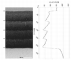
- the electron beam transmittance is lower as the film density is higher. For this reason, the portion where the film density is high is difficult to transmit the electron beam and becomes a dark image.
- the lower the film density the higher the electron beam transmittance, and the portion with the lower film density is more likely to transmit the electron beam, resulting in a brighter image. Therefore, it is considered that the change in contrast in the image has a correlation with the change in layer density.
- Example 1 Preparation of transparent resin film
- a transparent resin film resin substrate
- a polyethylene naphthalate film thickness 100 ⁇ m, trade name “Teonex” manufactured by Teijin DuPont Films was prepared.
- oxygen purity 5N: 99.999%) 10 sccm (10 ⁇ 1.69 ⁇ 10 ⁇ 3 Pa ⁇ m 3 / sec) and nitrogen (purity 5N: 99.999%) 20 sccm (20 ⁇ 1 .69 ⁇ 10 ⁇ 3 Pa ⁇ m 3 / second) into the vacuum chamber, and in this state, an electron beam (acceleration voltage: 6 kV) is applied to the silicon particles (purity: 3N: 99.9%) as a deposition material. An application current of 50 mA) was applied to evaporate the film to a deposition rate of 100 nm / min. At this time, the internal pressure was 2.0 ⁇ 10 ⁇ 2 Pa and the substrate heater temperature was 100 ° C.
- the process of rotating the substrate roll 13 leftward from the plasma gun 2 side (change in distance) in FIG. 5 and then rotating rightward (change in distance) from the focusing electrode 6 side was repeated five times. .
- the rotation speed of the substrate roll 13 was set to 0.5 m / min.
- FIG. 6 shows an image analysis result of the obtained transparent gas barrier layer.
- the maximum value of density in the transparent gas barrier layer was 2.68 g ⁇ cm ⁇ 3
- the minimum value was 2.30 g ⁇ cm ⁇ 3 .
- Ten layers whose density changed in the thickness direction were formed, and the thickness of each layer was about 30 nm.
- Example 2 The transparent gas barrier film of this example is the same as example 1 except that the positions of the end point of the left rotation and the start point of the right rotation are farther from the plasma gun 2 than in example 1. Got.
- the maximum value of the density in the transparent gas barrier layer was 2.68 g ⁇ cm ⁇ 3
- the minimum value was 2.20 g ⁇ cm ⁇ 3
- Ten layers whose density changed in the thickness direction were formed, and the thickness of each layer was about 30 nm.
- Example 3 The transparent gas barrier film of this example was the same as example 1 except that the end point of the left rotation and the start point of the right rotation were closer to the plasma gun 2 than in example 1. Got.
- the maximum value of the density in the transparent gas barrier layer was 2.68 g ⁇ cm ⁇ 3
- the minimum value was 2.45 g ⁇ cm ⁇ 3
- Ten layers whose density changed in the thickness direction were formed, and the thickness of each layer was about 30 nm.
- Example 4 The transparent gas barrier film of this example is the same as that of Example 1 except that the substrate roll 13 is rotated four times in one direction (change in distance) from the plasma gun 2 side in FIG. Got.
- FIG. 7 shows the image analysis result of the obtained transparent gas barrier layer.
- the maximum value of density in the transparent gas barrier layer was 2.68 g ⁇ cm ⁇ 3
- the minimum value was 2.30 g ⁇ cm ⁇ 3 .
- Four layers whose density changes in the thickness direction were formed, and the thickness of each layer was about 60 nm.
- a transparent gas barrier layer was formed by fixing the substrate roll 13 without rotating.
- Argon gas 20 sccm (20 ⁇ 1.69 ⁇ 10 ⁇ 3 Pa ⁇ m 3 / sec) was introduced into the pressure gradient plasma gun, and a discharge output of 5 kW was applied to the plasma gun to generate arc discharge plasma.
- oxygen purity 5N: 99.999%)
- nitrogen purity 5N: 99.999%)
- 20 sccm (20 ⁇ 1 .69 ⁇ 10 ⁇ 3 Pa ⁇ m 3 / second) into the vacuum chamber, and in this state, an electron beam (acceleration voltage: 6 kV) is applied to the silicon particles (purity: 3N: 99.9%) as a deposition material.
- An applied current of 50 mA was applied to evaporate the film to a deposition rate of 100 nm / min, and a silicon oxynitride layer was deposited on the substrate to a thickness of 50 nm.
- the discharge output applied to the plasma gun was set to 2 kW, and a silicon oxynitride layer was similarly deposited to a thickness of 50 nm.
- the internal pressure was 2.0 ⁇ 10 ⁇ 2 Pa and the substrate heater temperature was 100 ° C. This process was repeated alternately to form a total of 8 layers each having a thickness of 50 nm to obtain a transparent gas barrier film of this comparative example.
- the density of the layer formed with a discharge output of 5 kW was 2.68 g ⁇ cm ⁇ 3
- the density of the layer formed with a discharge output of 2 kW was 2.30 g ⁇ cm ⁇ 3 .
- a certain silicon grain (purity 3N: 99.9%) was irradiated with an electron beam (acceleration voltage 6 kV, applied current 50 mA) to evaporate to a deposition rate of 100 nm / min.
- the system internal pressure was 2.0 ⁇ 10 ⁇ 2 Pa
- the substrate heater temperature was 100 ° C.
- the process of rotating the substrate roll 13 leftward (change in distance) from the plasma gun 2 side in FIG. 5 and then rotating rightward (change in distance) from the reflective electrode 5 side is performed five times. Repeated.
- the rotation speed of the substrate roll 13 was set to 0.5 m / min.
- the thickness of each layer of the layers in which the atomic ratio changes in the thickness direction (10 layers in total) was 30 nm.
- FIG. 8 shows changes in the atomic ratio N / Si in the depth direction from the surface of the transparent gas barrier layer.
- the atomic ratio N / Si had a maximum value of 1.1 and a minimum value of 0.6.
- Example 6 Example 5 except that oxygen (purity 5N: 99.999%) was introduced as a reactive gas into the vacuum chamber at a flow rate of 30 sccm (30 ⁇ 1.69 ⁇ 10 ⁇ 3 Pa ⁇ m 3 / sec). In the same manner as above, a transparent gas barrier film of this example was obtained.
- the obtained transparent gas barrier layer was analyzed for the atomic ratio O / Si (X 2 O 3 / M) in the thickness direction within the layer.
- FIG. 9 shows changes in the atomic ratio O / Si in the depth direction from the surface of the transparent gas barrier layer.
- the atomic ratio O / Si had a maximum value of 1.8 and a minimum value of 1.2.
- Example 7 Example 5 except that methane (purity 4N: 99.99%) was introduced as a reactive gas into the vacuum chamber at a flow rate of 15 sccm (15 ⁇ 1.69 ⁇ 10 ⁇ 3 Pa ⁇ m 3 / sec). In the same manner as above, a transparent gas barrier film of this example was obtained.
- the prepared transparent gas barrier layer was analyzed in the thickness direction of the layer atomic ratio C / Si (X C / M ).
- FIG. 10 shows changes in the atomic ratio C / Si in the depth direction from the surface of the transparent gas barrier layer.
- the atomic ratio C / Si had a maximum value of 1.5 and a minimum value of 0.9.
- a transparent gas barrier layer was formed by fixing the substrate roll 13 without rotating.
- Argon gas 20 sccm (20 ⁇ 1.69 ⁇ 10 ⁇ 3 Pa ⁇ m 3 / sec) was introduced into the pressure gradient plasma gun, and a discharge output of 5 kW was applied to the plasma gun to generate arc discharge plasma.
- nitrogen nitrogen (purity 5N: 99.999%) was introduced into the vacuum chamber at a flow rate of 20 sccm (20 ⁇ 1.69 ⁇ 10 ⁇ 3 Pa ⁇ m 3 / sec).
- a silicon grain (purity 3N: 99.9%) is irradiated with an electron beam (acceleration voltage 6 kV, applied current 50 mA) and evaporated to a deposition rate of 100 nm / min to form a silicon nitride layer on the substrate. It vapor-deposited so that it might be set to 30 nm. Subsequently, the discharge output applied to the plasma gun was set to 2 kW, and a silicon nitride layer was similarly deposited to a thickness of 30 nm. At this time, the internal pressure was 2.0 ⁇ 10 ⁇ 2 Pa and the substrate heater temperature was 100 ° C. This process was repeated alternately to form a total of 10 layers each having a thickness of 30 nm to obtain a transparent gas barrier film of this comparative example.
- the obtained transparent gas barrier layer was analyzed for the atomic ratio N / Si in the thickness direction.
- the atomic ratio N / Si was constant at 1.2 regardless of the position in the thickness direction.
- Comparative Example 3 Comparative Example 2 except that oxygen (purity 5N: 99.999%) was introduced as a reactive gas into the vacuum chamber at a flow rate of 30 sccm (30 ⁇ 1.69 ⁇ 10 ⁇ 3 Pa ⁇ m 3 / sec). In the same manner, a transparent gas barrier film of this comparative example was obtained.
- the obtained transparent gas barrier layer was analyzed for atomic ratio O / Si in the thickness direction.
- the atomic ratio O / Si was constant at 1.8 regardless of the position in the thickness direction.
- Comparative Example 4 Comparative Example 2 except that methane (purity 4N: 99.99%) was introduced as a reactive gas into the vacuum chamber at a flow rate of 15 sccm (15 ⁇ 1.69 ⁇ 10 ⁇ 3 Pa ⁇ m 3 / sec). In the same manner, a transparent gas barrier film of this comparative example was obtained.
- the atomic ratio C / Si in the thickness direction of the obtained transparent gas barrier layer was analyzed.
- the atomic ratio C / Si was constant at 1.5 regardless of the position in the thickness direction.
- Comparative Example 1 the water vapor transmission rate before the bending test was as good as 0.005 g ⁇ m ⁇ 2 ⁇ day ⁇ 1 , but the water vapor transmission rate after the bending test was 0.010 g ⁇ m ⁇ 2 ⁇ day ⁇ . 1 and the gas barrier properties are deteriorated. In Comparative Example 1, it is considered that an internal stress difference between layers occurs, cracks are generated, and gas barrier properties are lowered.
- the transparent gas barrier films obtained in Examples 5 to 7 showed excellent gas barrier properties, and further, no change was seen in the water vapor transmission rate before and after the bending test, and good bending resistance. Also shown.
- Comparative Examples 2 to 4 it can be seen that the water vapor transmission rate after the bending test is larger than the water vapor transmission rate before the bending test, and the gas barrier properties are deteriorated. This is presumably because, in Comparative Examples 2 to 4, an internal stress difference between layers was generated, cracks were generated, and the gas barrier properties were lowered.
- the transparent gas barrier film of the present invention is excellent in gas barrier properties and has an extremely low internal stress in the transparent gas barrier layer.
- the transparent gas barrier film of the present invention is, for example, various display devices (displays) such as an organic EL display device, a field emission display device or a liquid crystal display device, various electric elements / electrical devices such as a solar cell, a thin film battery, and an electric double layer capacitor. It can be used as a flexible substrate or a sealing material of an element, and its use is not limited, and can be used in all fields in addition to the above-mentioned use.
Landscapes
- Chemical & Material Sciences (AREA)
- Chemical Kinetics & Catalysis (AREA)
- General Chemical & Material Sciences (AREA)
- Electrochemistry (AREA)
- Engineering & Computer Science (AREA)
- Materials Engineering (AREA)
- Inorganic Chemistry (AREA)
- Physics & Mathematics (AREA)
- Mechanical Engineering (AREA)
- Metallurgy (AREA)
- Organic Chemistry (AREA)
- Optics & Photonics (AREA)
- Composite Materials (AREA)
- Electromagnetism (AREA)
- Laminated Bodies (AREA)
- Electroluminescent Light Sources (AREA)
Abstract
Description
前記透明ガスバリア層が、金属および半金属からなる群から選ばれる少なくとも1種を含み、
前記透明ガスバリア層が、厚み方向に密度が連続的かつ周期的に変化する層を複数有しており、
前記密度の変化が、高密度から低密度への変化、または、低密度から高密度への変化であることを特徴とする。
前記透明ガスバリア層が、金属および半金属からなる群から選ばれる少なくとも1種と、酸素、窒素および炭素からなる群から選ばれる少なくとも1種とを含み、
前記透明ガスバリア層は、金属および半金属からなる群から選ばれる少なくとも1種の元素の含有割合(M(原子%))に対する酸素、窒素および炭素からなる群から選ばれる少なくとも1種の元素の含有割合(X(原子%))の比である原子比(X/M)が、厚み方向に連続的かつ周期的に変化する層を複数有しており、
前記原子比の変化が、大きい原子比から小さい原子比への変化、または、小さい原子比から大きい原子比への変化であることを特徴とする。
アーク放電プラズマを発生させ、反応ガスの存在下で金属酸化物および半金属酸化物の少なくとも一方を樹脂基板に蒸着させて透明ガスバリア層を形成する透明ガスバリア層形成工程を含み、
前記透明ガスバリア層形成工程において、前記樹脂基板とプラズマ源との距離を変化させながら蒸着を行い、
前記距離の変化が、前記距離を遠ざける変化、および、前記距離を近づける変化の少なくとも一方の変化であることを特徴とする。
さらに、背面封止部材を有し、
前記積層体の少なくとも一部が前記背面封止部材で被覆されており、
前記基板および前記背面封止部材の少なくとも一方が、前記本発明の透明ガスバリアフィルムであることを特徴とする。
前記金属および前記半金属からなる群から選ばれる少なくとも1種が、酸化物、窒化物、炭化物、酸化窒化物、酸化炭化物、窒化炭化物および酸化窒化炭化物からなる群から選ばれる少なくとも1種であることが好ましい。
水蒸気透過速度(WVTR)は、JIS K7126に規定される水蒸気透過速度測定装置(MOCON社製、商品名PERMATRAN)にて、温度40℃、湿度90%RHの環境下で測定した。なお、前記水蒸気透過率測定装置の測定範囲は、0.005g・m-2・day-1以上である。
円筒形マンドレル法(JIS K5600-5-1、コーテック社製試験装置を使用)により、透明ガスバリアフィルムの透明ガスバリア層側を外側にして、直径20mmのマンドレルにより1000回の折り曲げを実施したのち、前記と同様にWVTRを測定した。
透明ガスバリアフィルムを構成する各層の厚みは、透明ガスバリアフィルムの断面を、株式会社日本電子製の走査型電子顕微鏡(商品名:JSM-6610)にて観察し、基板(フィルム)表面から各層表面までの長さを測長し、算出した。
透明ガスバリアフィルムを構成する各層の密度ρは、株式会社リガク製のX線回折装置(商品名:Smart Lab)により、透明ガスバリア層を構成する各層のX線反射率を測定し、各層の密度を算出した。一般的に、電子線透過率は膜密度が高いほど低い。そのため、膜密度が高い部分は、電子線が透過しにくく、暗い像になる。一方、膜密度が低いほど電子線透過率は高くなり、膜密度が低い部分は、電子線が透過しやすく、明るい像になる。したがって、像におけるコントラストの変化は、層密度の変化と相関関係を有していると考えられる。
X線光電子スペクトル測定装置(アルバックファイ製)により、透明ガスバリア層の表面から一定の深さをArイオンエッチングし、厚み方向の原子比を測定することで、各層の原子比変化を測定した。
〔透明樹脂フィルムの準備〕
透明樹脂フィルム(樹脂基板)として、帝人デュポンフィルム社製のポリエチレンナフタレートフィルム(厚み100μm、商品名「テオネックス」)を準備した。
つぎに、前記ポリエチレンナフタレートフィルムを、図5に示す製造装置に装着した。圧力勾配型プラズマガン内にアルゴンガス20sccm(20×1.69×10-3Pa・m3/秒)を導入し、前記プラズマガンに5kWの放電出力を印加しアーク放電プラズマを発生させた。反応ガスとして、酸素(純度5N:99.999%)を10sccm(10×1.69×10-3Pa・m3/秒)および窒素(純度5N:99.999%)を20sccm(20×1.69×10-3Pa・m3/秒)の流量で真空槽内に導入し、この状態で、蒸着材料であるシリコン粒(純度3N:99.9%)に電子ビーム(加速電圧 6kV、印加電流 50mA)を照射して、蒸着速度100nm/minとなるように蒸発させた。このとき系内圧力が2.0×10-2Paで、基板加熱ヒータ温度は100℃とした。基板用ロール13を、図5においてプラズマガン2の側から左回転(距離を遠ざける変化)をさせ、ついで、収束電極6の側から右回転(距離を近づける変化)をさせる工程を5回繰り返した。基板用ロール13の回転速度は0.5m/minとなるようにした。
前記左回転の終点および前記右回転の開始点の位置を、実施例1に比べ、プラズマガン2からより遠い位置にしたこと以外は、実施例1と同様にして、本実施例の透明ガスバリアフィルムを得た。
前記左回転の終点および前記右回転の開始点の位置を、実施例1に比べ、プラズマガン2からより近い位置にしたこと以外は、実施例1と同様にして、本実施例の透明ガスバリアフィルムを得た。
基板用ロール13を、図5において、プラズマガン2の側から左回転の一方向(距離を遠ざける変化)で4回転させた以外は、実施例1と同様にして、本実施例の透明ガスバリアフィルムを得た。
基板用ロール13を回転させず、固定して透明ガスバリア層を形成した。圧力勾配型プラズマガン内にアルゴンガス20sccm(20×1.69×10-3Pa・m3/秒)を導入し、前記プラズマガンに5kWの放電出力を印加しアーク放電プラズマを発生させた。反応ガスとして、酸素(純度5N:99.999%)を10sccm(10×1.69×10-3Pa・m3/秒)および窒素(純度5N:99.999%)を20sccm(20×1.69×10-3Pa・m3/秒)の流量で真空槽内に導入し、この状態で、蒸着材料であるシリコン粒(純度3N:99.9%)に電子ビーム(加速電圧 6kV、印加電流 50mA)を照射して、蒸着速度100nm/minとなるように蒸発させて、基板上に酸化窒化シリコン層を厚み50nmとなるように蒸着した。ついで、前記プラズマガンに印加する放電出力を2kWにして、同様に、酸化窒化シリコン層を厚み50nmとなるように蒸着した。このとき系内圧力が2.0×10-2Paで、基板加熱ヒータ温度は100℃とした。このプロセスを交互に繰り返し、1層の厚みが50nmの層を計8層形成し、本比較例の透明ガスバリアフィルムを得た。
〔透明樹脂フィルムの準備〕
透明樹脂フィルム(樹脂基板)として、帝人デュポンフィルム社製のポリエチレンナフタレートフィルム(厚み100μm、商品名「テオネックス」)を準備した。
つぎに、前記ポリエチレンナフタレートフィルムを、図5に示す製造装置に装着した。圧力勾配型プラズマガン内にアルゴンガス20sccm(20×1.69×10-3Pa・m3/秒)を導入し、前記プラズマガンに5kWの放電出力を印加しアーク放電プラズマを発生させた。反応ガスとして、窒素(純度5N:99.999%)を20sccm(20×1.69×10-3Pa・m3/秒)の流量で真空槽内に導入し、この状態で、蒸着材料であるシリコン粒(純度3N:99.9%)に電子ビーム(加速電圧 6kV、印加電流 50mA)を照射して、蒸着速度100nm/minとなるように蒸発させた。このとき、系内圧力を2.0×10-2Pa、基板加熱ヒータ温度を100℃とした。基板用ロール13を、図5においてプラズマガン2の側から左回転(距離を遠ざける変化)をさせ、ついで、反射電極5の側から右回転(距離を近づける変化)をさせる工程を、各5回繰り返した。基板用ロール13の回転速度は0.5m/minとなるようにした。厚み方向に原子比が変化する層(計10層)の各層の厚みは、30nmであった。
反応性ガスとして、酸素(純度5N:99.999%)を30sccm(30×1.69×10-3Pa・m3/秒)の流量で真空槽内に導入したこと以外は、実施例5と同様にして、本実施例の透明ガスバリアフィルムを得た。
反応性ガスとして、メタン(純度4N:99.99%)を15sccm(15×1.69×10-3Pa・m3/秒)の流量で真空槽内に導入したこと以外は、実施例5と同様にして、本実施例の透明ガスバリアフィルムを得た。
基板用ロール13を回転させず、固定して透明ガスバリア層を形成した。圧力勾配型プラズマガン内にアルゴンガス20sccm(20×1.69×10-3Pa・m3/秒)を導入し、前記プラズマガンに5kWの放電出力を印加しアーク放電プラズマを発生させた。反応ガスとして、窒素(純度5N:99.999%)を20sccm(20×1.69×10-3Pa・m3/秒)の流量で真空槽内に導入し、この状態で、蒸着材料であるシリコン粒(純度3N:99.9%)に電子ビーム(加速電圧 6kV、印加電流 50mA)を照射して、蒸着速度100nm/minとなるように蒸発させて、基板上に窒化シリコン層を厚み30nmとなるように蒸着した。ついで、前記プラズマガンに印加する放電出力を2kWにして、同様に、窒化シリコン層を厚み30nmとなるように蒸着した。このとき系内圧力が2.0×10-2Paで、基板加熱ヒータ温度は100℃とした。このプロセスを交互に繰り返し、1層の厚みが30nmの層を計10層形成し、本比較例の透明ガスバリアフィルムを得た。
反応性ガスとして、酸素(純度5N:99.999%)を30sccm(30×1.69×10-3Pa・m3/秒)の流量で真空槽内に導入したこと以外は、比較例2と同様にして、本比較例の透明ガスバリアフィルムを得た。
反応性ガスとして、メタン(純度4N:99.99%)を15sccm(15×1.69×10-3Pa・m3/秒)の流量で真空槽内に導入したこと以外は、比較例2と同様にして、本比較例の透明ガスバリアフィルムを得た。


110 樹脂基板
120 透明ガスバリア層
500 製造装置
1 真空槽
2 圧力勾配型プラズマガン(アーク放電プラズマ発生源)
3 樹脂基板
4 プラズマビーム
5 反射電極
6 収束電極
7 蒸着源
8 蒸着材料
9 電子ビーム
10 水晶モニター
11 放電ガス供給手段
12 反応ガス供給手段
13 基板用ロール
20 真空ポンプ
21 放電ガス用ガスボンベ
22 反応ガス用ガスボンベ
Claims (16)
- 樹脂基板上に透明ガスバリア層が形成された透明ガスバリアフィルムであって、
前記透明ガスバリア層が、金属および半金属からなる群から選ばれる少なくとも1種を含み、
前記透明ガスバリア層が、厚み方向に密度が連続的かつ周期的に変化する層を複数有しており、
前記密度の変化が、高密度から低密度への変化、または、低密度から高密度への変化である
ことを特徴とする透明ガスバリアフィルム。 - 前記透明ガスバリア層における、密度の極小値(Dmin)に対する極大値(Dmax)の比(Dmax/Dmin)が、1.1以上であることを特徴とする、請求項1記載の透明ガスバリアフィルム。
- 前記厚み方向に密度が変化する層の各層の厚みが、50~200nmの範囲であることを特徴とする、請求項1または2記載の透明ガスバリアフィルム。
- 樹脂基板上に透明ガスバリア層が形成された透明ガスバリアフィルムであって、
前記透明ガスバリア層が、金属および半金属からなる群から選ばれる少なくとも1種と、酸素、窒素および炭素からなる群から選ばれる少なくとも1種とを含み、
前記透明ガスバリア層は、金属および半金属からなる群から選ばれる少なくとも1種の元素の含有割合(M(原子%))に対する酸素、窒素および炭素からなる群から選ばれる少なくとも1種の元素の含有割合(X(原子%))の比である原子比(X/M)が、厚み方向に連続的かつ周期的に変化する層を複数有しており、
前記原子比の変化が、大きい原子比から小さい原子比への変化、または、小さい原子比から大きい原子比への変化であることを特徴とする透明ガスバリアフィルム。 - 前記厚み方向に原子比が変化する層の各層の厚みが、20~200nmの範囲であることを特徴とする、請求項4記載の透明ガスバリアフィルム。
- 前記透明ガスバリア層において、金属および半金属元素からなる群から選ばれる少なくとも1種の元素の含有割合(M(原子%))に対する酸素の含有割合(XO(原子%))の比である原子比(XO/M)が、1~1.9の範囲であることを特徴とする、請求項4または5記載の透明ガスバリアフィルム。
- 前記透明ガスバリア層において、金属および半金属元素からなる群から選ばれる少なくとも1種の元素の含有割合(M(原子%))に対する窒素の含有割合(XN(原子%))の比である原子比(XN/M)が、0.5~1.2の範囲であることを特徴とする、請求項4から6のいずれか一項に記載の透明ガスバリアフィルム。
- 前記透明ガスバリア層において、金属および半金属元素からなる群から選ばれる少なくとも1種の元素の含有割合(M(原子%))に対する炭素の含有割合(XC(原子%))の比である原子比(XC/M)が、0.5~1.7の範囲であることを特徴とする、請求項4から7のいずれか一項に記載の透明ガスバリアフィルム。
- 前記金属および前記半金属からなる群から選ばれる少なくとも1種が、酸化物、窒化物、炭化物、酸化窒化物、酸化炭化物、窒化炭化物および酸化窒化炭化物からなる群から選ばれる少なくとも1種であることを特徴とする、請求項1から8のいずれか一項に記載の透明ガスバリアフィルム。
- 樹脂基板上に透明ガスバリア層を形成する透明ガスバリアフィルムの製造方法であって、
アーク放電プラズマを発生させ、反応ガスの存在下で金属酸化物および半金属酸化物の少なくとも一方を樹脂基板に蒸着させて透明ガスバリア層を形成する透明ガスバリア層形成工程を含み、
前記透明ガスバリア層形成工程において、前記樹脂基板とプラズマ源との距離を変化させながら蒸着を行い、
前記距離の変化が、前記距離を遠ざける変化、および、前記距離を近づける変化の少なくとも一方の変化であることを特徴とする、透明ガスバリアフィルムの製造方法。 - 前記距離の変化を繰り返しながら、前記透明ガスバリア層形成工程を行うことを特徴とする、請求項10記載の透明ガスバリアフィルムの製造方法。
- 請求項10または11記載の透明ガスバリアフィルムの製造方法によって製造されたことを特徴とする透明ガスバリアフィルム。
- 基板上に、陽極層、有機EL層および陰極層が、この順序で設けられた積層体を有する有機EL素子であって、前記基板が、請求項1から9のいずれか一項または請求項12記載の透明ガスバリアフィルムであることを特徴とする有機EL素子。
- 基板上に、陽極層、有機EL層および陰極層が、この順序で設けられた積層体を有する有機EL素子であって、
さらに、背面封止部材を有し、
前記積層体の少なくとも一部が前記背面封止部材で被覆されており、
前記基板および前記背面封止部材の少なくとも一方が、請求項1から9のいずれか一項または請求項12記載の透明ガスバリアフィルムであることを特徴とする、有機EL素子。 - 太陽電池セルを含む太陽電池であって、前記太陽電池セルが、請求項1から9のいずれか一項または請求項12記載の透明ガスバリアフィルムで被覆されていることを特徴とする太陽電池。
- 集電層、陽極層、固体電解質層、陰極層および集電層が、この順序で設けられた積層体を有する薄膜電池であって、前記積層体が、請求項1から9のいずれか一項または請求項12記載の透明ガスバリアフィルムで被覆されていることを特徴とする薄膜電池。
Priority Applications (4)
| Application Number | Priority Date | Filing Date | Title |
|---|---|---|---|
| KR1020147016360A KR20140106567A (ko) | 2011-12-27 | 2012-12-14 | 투명 가스 배리어 필름, 투명 가스 배리어 필름의 제조 방법, 유기 el 소자, 태양 전지 및 박막 전지 |
| US14/364,945 US9660208B2 (en) | 2011-12-27 | 2012-12-14 | Transparent gas barrier film, method for producing transparent gas barrier film, organic EL element, solar battery, and thin film battery |
| CN201280051657.XA CN103906625A (zh) | 2011-12-27 | 2012-12-14 | 透明阻气膜、透明阻气膜的制造方法、有机el元件、太阳能电池以及薄膜电池 |
| EP12861425.2A EP2799225A4 (en) | 2011-12-27 | 2012-12-14 | TRANSLUCENT GAS REINFORCING METHOD, METHOD FOR PRODUCING A TRANSPARENT GAS TAPE, ORGANIC EL-ELEMENT, SOLAR CELL AND THIN-LAYER CELL |
Applications Claiming Priority (4)
| Application Number | Priority Date | Filing Date | Title |
|---|---|---|---|
| JP2011286943A JP5892789B2 (ja) | 2011-12-27 | 2011-12-27 | 透明ガスバリアフィルム、透明ガスバリアフィルムの製造方法、有機el素子、太陽電池および薄膜電池 |
| JP2011-286943 | 2011-12-27 | ||
| JP2012045293A JP2013180473A (ja) | 2012-03-01 | 2012-03-01 | 透明ガスバリアフィルム、有機el素子、太陽電池および薄膜電池 |
| JP2012-045293 | 2012-03-01 |
Publications (1)
| Publication Number | Publication Date |
|---|---|
| WO2013099654A1 true WO2013099654A1 (ja) | 2013-07-04 |
Family
ID=48697146
Family Applications (1)
| Application Number | Title | Priority Date | Filing Date |
|---|---|---|---|
| PCT/JP2012/082474 Ceased WO2013099654A1 (ja) | 2011-12-27 | 2012-12-14 | 透明ガスバリアフィルム、透明ガスバリアフィルムの製造方法、有機el素子、太陽電池および薄膜電池 |
Country Status (6)
| Country | Link |
|---|---|
| US (1) | US9660208B2 (ja) |
| EP (1) | EP2799225A4 (ja) |
| KR (1) | KR20140106567A (ja) |
| CN (1) | CN103906625A (ja) |
| TW (2) | TWI501873B (ja) |
| WO (1) | WO2013099654A1 (ja) |
Families Citing this family (11)
| Publication number | Priority date | Publication date | Assignee | Title |
|---|---|---|---|---|
| KR102373437B1 (ko) | 2015-03-05 | 2022-03-14 | 삼성디스플레이 주식회사 | 유기발광표시장치 및 그 제조방법 |
| US10461270B2 (en) | 2016-03-29 | 2019-10-29 | Sharp Kabushiki Kaisha | Organic EL display device |
| JP6723051B2 (ja) * | 2016-03-31 | 2020-07-15 | 住友化学株式会社 | 積層フィルム及びその製造方法、並びに、積層フィルムの分析方法 |
| KR102343390B1 (ko) | 2017-04-03 | 2021-12-28 | 삼성디스플레이 주식회사 | 표시 장치 및 이의 제조 방법 |
| CN111480259B (zh) | 2018-02-26 | 2023-11-03 | 株式会社村田制作所 | 全固体电池 |
| JP7354092B2 (ja) | 2018-03-16 | 2023-10-02 | マクセル株式会社 | シート状電池、および、パッチ |
| JP7426628B2 (ja) * | 2018-08-28 | 2024-02-02 | パナソニックIpマネジメント株式会社 | コンデンサ及びその製造方法 |
| ES3040230T3 (en) * | 2019-02-19 | 2025-10-29 | Xefco Pty Ltd | System for treatment and/or coating of substrates |
| BR112021021780A2 (pt) * | 2019-05-31 | 2021-12-21 | Toyo Boseki | Filme de barreira ao gás transparente e método para produção do mesmo |
| CN112736204B (zh) * | 2020-12-30 | 2021-08-06 | 山东永聚医药科技有限公司 | 金属诱导非晶结晶化转变超高阻隔膜及其制备方法 |
| CN117549611B (zh) * | 2023-11-24 | 2024-05-03 | 江苏天鸟高新技术股份有限公司 | 一种梯度密度预制体及其制备方法和隔热材料 |
Citations (9)
| Publication number | Priority date | Publication date | Assignee | Title |
|---|---|---|---|---|
| JPH08164595A (ja) | 1994-12-15 | 1996-06-25 | Toppan Printing Co Ltd | 透明積層フィルム |
| JP2996516B2 (ja) | 1996-04-04 | 2000-01-11 | シグマ ラボラトリーズ オブ アリゾナ インコーポレーテッド | ハイブリッドポリマーフィルム |
| JP2004151528A (ja) | 2002-10-31 | 2004-05-27 | Bridgestone Corp | 薄膜表示素子保護用バリヤー膜 |
| JP2005171304A (ja) * | 2003-12-10 | 2005-06-30 | Dainippon Printing Co Ltd | バリアフィルムの製造方法 |
| WO2006033233A1 (ja) * | 2004-09-21 | 2006-03-30 | Konica Minolta Holdings, Inc. | 透明ガスバリア性フィルム |
| JP2007230115A (ja) | 2006-03-02 | 2007-09-13 | Nitto Denko Corp | 透明ガスバリア性フィルムの製造方法、透明ガスバリア性フィルムおよび透明ガスバリア性フィルムの製造装置 |
| WO2008096615A1 (ja) * | 2007-02-05 | 2008-08-14 | Konica Minolta Holdings, Inc. | 透明ガスバリア性フィルム及びその製造方法 |
| WO2008096616A1 (ja) * | 2007-02-05 | 2008-08-14 | Konica Minolta Holdings, Inc. | 透明ガスバリア性フィルム及びその製造方法 |
| JP2009023284A (ja) | 2007-07-23 | 2009-02-05 | Toppan Printing Co Ltd | ガスバリア性積層フィルム |
Family Cites Families (14)
| Publication number | Priority date | Publication date | Assignee | Title |
|---|---|---|---|---|
| US7015640B2 (en) | 2002-09-11 | 2006-03-21 | General Electric Company | Diffusion barrier coatings having graded compositions and devices incorporating the same |
| US20050037240A1 (en) | 2003-03-31 | 2005-02-17 | Daisaku Haoto | Protective coat and method for manufacturing thereof |
| JP4526848B2 (ja) | 2003-03-31 | 2010-08-18 | 大日本印刷株式会社 | 保護膜およびその製造方法 |
| US7648925B2 (en) * | 2003-04-11 | 2010-01-19 | Vitex Systems, Inc. | Multilayer barrier stacks and methods of making multilayer barrier stacks |
| JP5244622B2 (ja) | 2009-01-08 | 2013-07-24 | 三菱樹脂株式会社 | ガスバリア性フィルム |
| WO2010100971A1 (ja) | 2009-03-04 | 2010-09-10 | コニカミノルタホールディングス株式会社 | 薄膜を有する基材 |
| JP5470969B2 (ja) | 2009-03-30 | 2014-04-16 | 株式会社マテリアルデザインファクトリ− | ガスバリアフィルム、それを含む電子デバイス、ガスバリア袋、およびガスバリアフィルムの製造方法 |
| KR101718560B1 (ko) | 2009-04-09 | 2017-03-21 | 스미또모 가가꾸 가부시키가이샤 | 가스 배리어성 적층 필름 |
| JP5580561B2 (ja) * | 2009-09-01 | 2014-08-27 | 富士フイルム株式会社 | バリア性積層体、ガスバリアフィルムおよびバリア性積層体の製造方法 |
| JP5570170B2 (ja) | 2009-09-29 | 2014-08-13 | 富士フイルム株式会社 | ガスバリアユニット、太陽電池モジュール用のバックシート、および太陽電池モジュール |
| EP2360293A1 (en) | 2010-02-11 | 2011-08-24 | Nederlandse Organisatie voor toegepast -natuurwetenschappelijk onderzoek TNO | Method and apparatus for depositing atomic layers on a substrate |
| US9297076B2 (en) | 2010-07-23 | 2016-03-29 | Lotus Applied Technology, Llc | Substrate transport mechanism contacting a single side of a flexible web substrate for roll-to-roll thin film deposition |
| JP5544271B2 (ja) | 2010-10-19 | 2014-07-09 | 株式会社フジクラ | 酸化物超電導体薄膜の成膜方法および成膜装置 |
| JP2014154361A (ja) * | 2013-02-08 | 2014-08-25 | Nitto Denko Corp | 透明ガスバリアフィルムの製造方法、透明ガスバリアフィルムの製造装置、及び有機エレクトロルミネッセンスデバイス |
-
2012
- 2012-12-13 TW TW101147174A patent/TWI501873B/zh not_active IP Right Cessation
- 2012-12-13 TW TW103133962A patent/TWI530399B/zh not_active IP Right Cessation
- 2012-12-14 KR KR1020147016360A patent/KR20140106567A/ko not_active Withdrawn
- 2012-12-14 CN CN201280051657.XA patent/CN103906625A/zh active Pending
- 2012-12-14 EP EP12861425.2A patent/EP2799225A4/en not_active Withdrawn
- 2012-12-14 WO PCT/JP2012/082474 patent/WO2013099654A1/ja not_active Ceased
- 2012-12-14 US US14/364,945 patent/US9660208B2/en not_active Expired - Fee Related
Patent Citations (9)
| Publication number | Priority date | Publication date | Assignee | Title |
|---|---|---|---|---|
| JPH08164595A (ja) | 1994-12-15 | 1996-06-25 | Toppan Printing Co Ltd | 透明積層フィルム |
| JP2996516B2 (ja) | 1996-04-04 | 2000-01-11 | シグマ ラボラトリーズ オブ アリゾナ インコーポレーテッド | ハイブリッドポリマーフィルム |
| JP2004151528A (ja) | 2002-10-31 | 2004-05-27 | Bridgestone Corp | 薄膜表示素子保護用バリヤー膜 |
| JP2005171304A (ja) * | 2003-12-10 | 2005-06-30 | Dainippon Printing Co Ltd | バリアフィルムの製造方法 |
| WO2006033233A1 (ja) * | 2004-09-21 | 2006-03-30 | Konica Minolta Holdings, Inc. | 透明ガスバリア性フィルム |
| JP2007230115A (ja) | 2006-03-02 | 2007-09-13 | Nitto Denko Corp | 透明ガスバリア性フィルムの製造方法、透明ガスバリア性フィルムおよび透明ガスバリア性フィルムの製造装置 |
| WO2008096615A1 (ja) * | 2007-02-05 | 2008-08-14 | Konica Minolta Holdings, Inc. | 透明ガスバリア性フィルム及びその製造方法 |
| WO2008096616A1 (ja) * | 2007-02-05 | 2008-08-14 | Konica Minolta Holdings, Inc. | 透明ガスバリア性フィルム及びその製造方法 |
| JP2009023284A (ja) | 2007-07-23 | 2009-02-05 | Toppan Printing Co Ltd | ガスバリア性積層フィルム |
Non-Patent Citations (1)
| Title |
|---|
| See also references of EP2799225A4 |
Also Published As
| Publication number | Publication date |
|---|---|
| TW201501947A (zh) | 2015-01-16 |
| TWI530399B (zh) | 2016-04-21 |
| US20140308580A1 (en) | 2014-10-16 |
| US9660208B2 (en) | 2017-05-23 |
| TW201331041A (zh) | 2013-08-01 |
| KR20140106567A (ko) | 2014-09-03 |
| CN103906625A (zh) | 2014-07-02 |
| EP2799225A1 (en) | 2014-11-05 |
| TWI501873B (zh) | 2015-10-01 |
| EP2799225A4 (en) | 2015-08-26 |
Similar Documents
| Publication | Publication Date | Title |
|---|---|---|
| WO2013099654A1 (ja) | 透明ガスバリアフィルム、透明ガスバリアフィルムの製造方法、有機el素子、太陽電池および薄膜電池 | |
| US20150147471A1 (en) | Method for producing transparent gas barrier film and apparatus for producing transparent gas barrier film | |
| US20090286071A1 (en) | Transparent conductive film and method for production thereof | |
| MXPA01010917A (es) | Dispositivo electronico organico flexible con resistencia mejorada a la degradacion por oxigeno y humedad. | |
| JP5740179B2 (ja) | 透明ガスバリアフィルム、透明ガスバリアフィルムの製造方法、有機エレクトロルミネッセンス素子、太陽電池および薄膜電池 | |
| JP2013180473A (ja) | 透明ガスバリアフィルム、有機el素子、太陽電池および薄膜電池 | |
| US9704610B2 (en) | Manganese tin oxide based transparent conducting oxide and transparent conductive film and method for fabricating transparent conductive film using the same | |
| US20150333289A1 (en) | Method for producing transparent gas barrier film, apparatus for producing transparent gas barrier film, and organic electroluminescence device | |
| JP2012206380A (ja) | 透明ガスバリアフィルム、透明ガスバリアフィルムの製造方法、有機エレクトロルミネッセンス素子、太陽電池および薄膜電池 | |
| US20080000388A1 (en) | Gas Barrier Transparent Resin Substrate Method for Manufacturing Thereof, and Flexible Display Element Using Barrier Transparent Resin Substrate | |
| JP5892789B2 (ja) | 透明ガスバリアフィルム、透明ガスバリアフィルムの製造方法、有機el素子、太陽電池および薄膜電池 | |
| JP5114683B2 (ja) | 太陽電池用ガラス基板の裏面電極及びその製造方法 | |
| JP6057450B2 (ja) | Ito透明導電膜付き基板およびその製造方法 | |
| JP2013022820A (ja) | 透明ガスバリアフィルム、透明ガスバリアフィルムの製造方法、有機エレクトロルミネッセンス素子、太陽電池および薄膜電池 | |
| JP2012179762A (ja) | 透明ガスバリアフィルム、透明ガスバリアフィルムの製造方法、有機エレクトロルミネッセンス素子、太陽電池および薄膜電池 | |
| JP2012206381A (ja) | 透明ガスバリアフィルム、透明ガスバリアフィルムの製造方法、有機エレクトロルミネッセンス素子、太陽電池および薄膜電池 | |
| JP2008240131A (ja) | 透明ガスバリアフィルムおよびエレクトロルミネッセンス素子 | |
| KR101719520B1 (ko) | 탄화불소 박막을 포함하는 다층 배리어 필름 및 이의 제조방법 | |
| JP5779815B2 (ja) | 電池セル | |
| JP2006114263A (ja) | 透明導電積層体 | |
| JP2012212577A (ja) | 透明ガスバリア層の製造方法、透明ガスバリア層、透明ガスバリアフィルム、有機エレクトロルミネッセンス素子、太陽電池および薄膜電池 | |
| JP2012211373A (ja) | 透明ガスバリアフィルム、透明ガスバリアフィルムの製造方法、有機エレクトロルミネッセンス素子、太陽電池および薄膜電池 | |
| CN110114897A (zh) | 电子设备 | |
| JP2012207268A (ja) | 透明ガスバリア層の製造方法、透明ガスバリア層、透明ガスバリアフィルム、有機エレクトロルミネッセンス素子、太陽電池および薄膜電池 | |
| JP2012207269A (ja) | 透明ガスバリア層の製造方法、透明ガスバリア層、透明ガスバリアフィルム、有機エレクトロルミネッセンス素子、太陽電池および薄膜電池 |
Legal Events
| Date | Code | Title | Description |
|---|---|---|---|
| 121 | Ep: the epo has been informed by wipo that ep was designated in this application |
Ref document number: 12861425 Country of ref document: EP Kind code of ref document: A1 |
|
| WWE | Wipo information: entry into national phase |
Ref document number: 14364945 Country of ref document: US |
|
| ENP | Entry into the national phase |
Ref document number: 20147016360 Country of ref document: KR Kind code of ref document: A |
|
| NENP | Non-entry into the national phase |
Ref country code: DE |
|
| WWE | Wipo information: entry into national phase |
Ref document number: 2012861425 Country of ref document: EP |