WO2013103063A1 - Boîtier de réception de lumière pour plaque à plat, et module optique - Google Patents
Boîtier de réception de lumière pour plaque à plat, et module optique Download PDFInfo
- Publication number
- WO2013103063A1 WO2013103063A1 PCT/JP2012/081396 JP2012081396W WO2013103063A1 WO 2013103063 A1 WO2013103063 A1 WO 2013103063A1 JP 2012081396 W JP2012081396 W JP 2012081396W WO 2013103063 A1 WO2013103063 A1 WO 2013103063A1
- Authority
- WO
- WIPO (PCT)
- Prior art keywords
- light
- flat
- holder
- monitor
- substrate
- Prior art date
- Legal status (The legal status is an assumption and is not a legal conclusion. Google has not performed a legal analysis and makes no representation as to the accuracy of the status listed.)
- Ceased
Links
Images


Classifications
-
- G—PHYSICS
- G02—OPTICS
- G02B—OPTICAL ELEMENTS, SYSTEMS OR APPARATUS
- G02B6/00—Light guides; Structural details of arrangements comprising light guides and other optical elements, e.g. couplings
- G02B6/24—Coupling light guides
- G02B6/42—Coupling light guides with opto-electronic elements
- G02B6/4295—Coupling light guides with opto-electronic elements coupling with semiconductor devices activated by light through the light guide, e.g. thyristors, phototransistors
-
- G—PHYSICS
- G02—OPTICS
- G02B—OPTICAL ELEMENTS, SYSTEMS OR APPARATUS
- G02B6/00—Light guides; Structural details of arrangements comprising light guides and other optical elements, e.g. couplings
- G02B6/10—Light guides; Structural details of arrangements comprising light guides and other optical elements, e.g. couplings of the optical waveguide type
- G02B6/12—Light guides; Structural details of arrangements comprising light guides and other optical elements, e.g. couplings of the optical waveguide type of the integrated circuit kind
-
- G—PHYSICS
- G02—OPTICS
- G02B—OPTICAL ELEMENTS, SYSTEMS OR APPARATUS
- G02B6/00—Light guides; Structural details of arrangements comprising light guides and other optical elements, e.g. couplings
- G02B6/10—Light guides; Structural details of arrangements comprising light guides and other optical elements, e.g. couplings of the optical waveguide type
- G02B6/12—Light guides; Structural details of arrangements comprising light guides and other optical elements, e.g. couplings of the optical waveguide type of the integrated circuit kind
- G02B6/13—Integrated optical circuits characterised by the manufacturing method
-
- G—PHYSICS
- G02—OPTICS
- G02B—OPTICAL ELEMENTS, SYSTEMS OR APPARATUS
- G02B6/00—Light guides; Structural details of arrangements comprising light guides and other optical elements, e.g. couplings
- G02B6/24—Coupling light guides
- G02B6/42—Coupling light guides with opto-electronic elements
- G02B6/4201—Packages, e.g. shape, construction, internal or external details
- G02B6/4202—Packages, e.g. shape, construction, internal or external details for coupling an active element with fibres without intermediate optical elements, e.g. fibres with plane ends, fibres with shaped ends, bundles
- G02B6/4203—Optical features
-
- G—PHYSICS
- G02—OPTICS
- G02B—OPTICAL ELEMENTS, SYSTEMS OR APPARATUS
- G02B6/00—Light guides; Structural details of arrangements comprising light guides and other optical elements, e.g. couplings
- G02B6/24—Coupling light guides
- G02B6/42—Coupling light guides with opto-electronic elements
- G02B6/4201—Packages, e.g. shape, construction, internal or external details
- G02B6/4256—Details of housings
- G02B6/4262—Details of housings characterised by the shape of the housing
- G02B6/4265—Details of housings characterised by the shape of the housing of the Butterfly or dual inline package [DIP] type
-
- G—PHYSICS
- G02—OPTICS
- G02B—OPTICAL ELEMENTS, SYSTEMS OR APPARATUS
- G02B6/00—Light guides; Structural details of arrangements comprising light guides and other optical elements, e.g. couplings
- G02B6/24—Coupling light guides
- G02B6/42—Coupling light guides with opto-electronic elements
- G02B6/4201—Packages, e.g. shape, construction, internal or external details
- G02B6/4286—Optical modules with optical power monitoring
-
- H—ELECTRICITY
- H10—SEMICONDUCTOR DEVICES; ELECTRIC SOLID-STATE DEVICES NOT OTHERWISE PROVIDED FOR
- H10F—INORGANIC SEMICONDUCTOR DEVICES SENSITIVE TO INFRARED RADIATION, LIGHT, ELECTROMAGNETIC RADIATION OF SHORTER WAVELENGTH OR CORPUSCULAR RADIATION
- H10F77/00—Constructional details of devices covered by this subclass
- H10F77/50—Encapsulations or containers
-
- G—PHYSICS
- G02—OPTICS
- G02B—OPTICAL ELEMENTS, SYSTEMS OR APPARATUS
- G02B6/00—Light guides; Structural details of arrangements comprising light guides and other optical elements, e.g. couplings
- G02B6/10—Light guides; Structural details of arrangements comprising light guides and other optical elements, e.g. couplings of the optical waveguide type
- G02B6/12—Light guides; Structural details of arrangements comprising light guides and other optical elements, e.g. couplings of the optical waveguide type of the integrated circuit kind
- G02B2006/12133—Functions
- G02B2006/12138—Sensor
Definitions
- the present invention relates to a light receiving package for flat plate placement on which a monitor PD (Photo Diode) is mounted, and an optical module.
- monitor PD Photo Diode
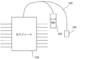
- the conventional monitor PD 102 has a coaxial structure with a fiber, and as shown in FIG. 6, the optical signal is tapped to the optical fiber 103 of the optical module 101 and connected by fusion or the like to monitor the output of the optical signal (See, for example, Patent Document 1).
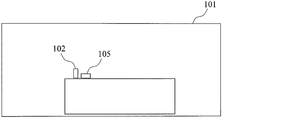
- FIG. 7 shows a conventional example in which the monitor PD 102 is integrated inside the optical module 101 (see, for example, Patent Document 2).
- the monitor PD 102 has a form in which a PD bare chip is mounted on a carrier such as ceramic.
- this invention aims at provision of the light reception package for flat plate arrangement
- the light receiving package for flat plate placement of the present invention has a light receiver and a holding holder, the light receiver is fixed to the front of the holding holder, and the back surface of the holding holder is of the light receiver.
- the first subassembly is a flat surface movable in parallel on a plane parallel to the light receiving surface, a U-shaped concave holder for holding the holding holder, and a flat base disposed on the substrate.
- the mounting surface of the flat plate base on the substrate is a flat surface movable in parallel with the substrate surface, and the concave holder and the flat plate face each other with the notched side of the concave holder above the substrate.
- a second sub-assembly in which a base is fixed, and at least one surface of the U-shaped surface of the concave holder is a flat surface capable of translating the back surface of the holding holder.
- the second subassembly includes a flat base, which allows the receiver to be installed at a desired position on the substrate.
- the second subassembly includes the concave holder, and the first subassembly includes the holding holder, thereby translating the light receiver on a plane parallel to the light receiving surface of the light receiver, and adjusting the light receiving sensitivity of the monitor PD.
- the monitor PD can be fixed at the position.
- the reception sensitivity of the monitor PD can be made constant and stable. Therefore, in the light receiving package for flat plate placement of the present invention, the reception sensitivity can be made constant without increasing the size of the module.
- the optical module according to the present invention comprises a waveguide type optical element mounted on the substrate and guiding light from the optical fiber, and a part of the light propagating through the waveguide type optical element being separated and the waveguide type And a light receiving package for flat plate placement according to the present invention for receiving monitor light emitted from the optical element.
- the optical module of the present invention includes the light receiving package for flat plate placement of the present invention, so that even if the monitor PD is disposed in the optical module, the reception sensitivity of the monitor PD can be made constant. Therefore, in the optical module of the present invention, the reception sensitivity can be made constant without increasing the size of the module.
- the waveguided optical element is provided with an emission window for emitting the monitor light at an end face connected to the optical fiber, and a light receiver of the flat panel arrangement light receiving package is the monitor light
- the exit window and the entrance window may be disposed opposite to each other.
- the optical module of the present invention since the exit window is disposed at the end face of the waveguide type optical element connected to the optical fiber, stray light entering the entrance window can be reduced.
- the optical module of the present invention can accurately monitor signal light.
- the waveguided optical element is connected to two optical fibers, and the exit window emits monitor light from which part of the light from one of the optical fibers is separated,
- the exit window and the entrance window may pass the monitor light and block stray light in the waveguided optical element.
- the optical module of the present invention can extract only the signal light as monitor light from the exit window when the signal light and the local light are incident on the waveguide type optical element.
- the emission window and the incidence window allow the monitor light to pass and block stray light in the waveguide type optical element, so that only the monitor light from which the signal light is separated can be made incident on the monitor PD.
- the optical module of the present invention can accurately monitor signal light.
- the present invention it is possible to provide a flat panel light receiving package and an optical module that can make the reception sensitivity of the monitor PD constant and stable without increasing the size of the module.
- the top view of the optical module concerning this embodiment is shown.
- the A-A 'sectional view of the optical module concerning this embodiment is shown. It is a side view of the light reception package for flat board arrangement concerning this embodiment. It is a rear view of the light reception package for flat plate arrangement concerning this embodiment.
- An example of the light receiver which concerns on this embodiment is shown.
- the example of mounting of monitor PD of patent document 1 is shown.
- the example of mounting of monitor PD of patent document 2 is shown.
- the optical module according to the present embodiment is an integrated reception FE module compatible with optical phase modulation according to the further increase in communication traffic, that is, the DQPSK transmission system or the DP-QPSK transmission system.
- the PLC receiving optical circuit used in these transmission methods is called a delay interferometer DLI (Delay Line Interferometer) or DPOH (Dual Polarization Optical Hybrid), and converts differences in optical signal phase state into differences in light intensity.
- This is an optical module integrated with a high frequency amplifier that receives and demodulates it with a PD that can detect only the intensity difference, current / voltage converts and amplifies the electric signal demodulated by the PD, and outputs it as a high frequency electric signal.
- FIG. 1 and 2 show an example of an optical module according to the present embodiment.
- FIG. 1 is a top view of the optical module according to the present embodiment
- FIG. 2 is a side view of the optical module according to the present embodiment.
- the optical module according to this embodiment includes a substrate 11, an optical semiconductor package 12, a PLC reception optical circuit 13 as a waveguide type optical element, an optical lens 14, a lens holding holder 17, and a light receiving package 30 for flat plate arrangement.
- the optical semiconductor package 12 includes a receiving unit for demodulation, and the flat-plate placement light receiving package 30 includes a monitor PD.
- the optical signal transmitted from the optical fiber 16 is incident on the PLC reception optical circuit 13.
- the PLC reception optical circuit 13 is mounted on the substrate 11 and guides the light from the optical fiber 16.
- the waveguide is separated (Tap) in the PLC reception optical circuit 13 and separated into an optical signal traveling to the receiving unit for demodulation and an optical signal traveling toward the monitor PD.
- An optical signal traveling to the monitor PD is monitor light, and is emitted from an emission window 34 disposed at an end face connected to the optical fiber 16.
- the emission window 34 serving as the PLC emission end is obliquely cut to prevent reflection, and an AR plate is mounted. Thereby, the reflection which is a noise component can be suppressed.
- the light signal for monitor PD reception that is, the monitor light is output from the emission window 34 disposed on the side of the fiber input unit 33, and the light receiving package 30 for flat plate arrangement from the incident window 53 disposed facing the emission window 34. It enters into the inside monitor PD.
- the monitor PD of the light receiving package 30 for flat plate arrangement receives the monitor light incident from the incident window 53, and light sensitivity can be obtained.
- FIGS. 3 and 4 show an example of the light receiving package 30 for flat plate placement.
- FIG. 3 is a side view of the light receiving package for flat plate placement according to the present embodiment
- FIG. 4 is a back view of the light receiving package for flat plate placement according to the present embodiment.
- the flat-plate placement light-receiving package 30 according to this embodiment includes a first subassembly 31 and a second subassembly 32.
- the first subassembly 31 comprises a light receiver 41 and a holding holder 42.
- the second subassembly 32 includes a U-shaped concave holder 43 and a flat plate base 44.
- the light receiver 41 includes a monitor PD 51 mounted on a small CAN-PKG (Package).
- the monitor PD 51 is mounted in a small CAN-PKG formed of a flat plate base 54, a cap 52, and an incident window 53, and is hermetically sealed. Therefore, it is possible to perform stable operation even when mounted inside an unsealed optical module.
- the light receiver 41 can be aligned inside the optical module, and stable reception sensitivity can always be obtained. Indirect parts such as lenses may be mounted on a small CAN-PKG. In addition, sufficient crosstalk can be secured for stray light by controlling the effective window of the small CAN-PKG and the effective diameter of the lens.
- the entrance window 53 of the small CAN-PKG on which the monitor PD 51 is mounted may be flat glass or a lens.
- the entrance window 53 has a predetermined opening. This can suppress the incidence of stray light inside the module and the incidence of local light. As a result, it is possible to obtain the reception sensitivity in which the noise component is suppressed.
- the mounting structure first fixes the light receiver 41 to the alignment holding holder 42 to make the first subassembly 31.
- the holding holder 42 is preferably a metal material such as Fe-Ni-Co.
- a fixing method an adhesive, laser welding or the like can be used.
- the concave holder 43 is fixed at a predetermined position of the flat plate base 44 to make the second subassembly 32.
- the concave holder 43 and the flat plate base 44 are fixed with the side with the notch of the concave holder 43 directed upward of the substrate 11.
- the concave holder 43 is fixed on the flat plate base 44 with an adhesive or the like.
- the concave holder 43 is preferably a metal material such as Fe-Ni-Co.
- the flat plate base 44 is preferably made of alumina.
- the second subassembly 32 is fixed with an adhesive or the like at a predetermined position on the substrate 11 for holding the first subassembly 31.
- a mounting surface of the flat plate base 44 on the substrate 11 is a flat surface movable in parallel with the substrate surface, and can be disposed at a predetermined position on the substrate 11.
- the back surface 45 of the holding holder 42 facing the incident window 53 is brought into contact with the PLC side flat surface 46 of the concave holder 43 of the second subassembly 32 inside the optical module to perform optical alignment. Since the PLC side flat surface 46 disposed on the PLC receiving optical circuit 13 side of the U-shaped surface of the concave holder 43 is a flat surface among the U-shaped surfaces of the concave holder 43, the rear surface of the holding holder 42 is 45 and the PLC side flat surface 46 of the concave holder 43 can be rubbed together to perform optical alignment in the xy plane parallel to the light receiving surface of the monitor PD 51.
- the PLC reception optical circuit 13 may be connected to the two optical fibers 16. For example, one optical fiber 16 enters signal light into the PLC reception optical circuit 13, and the other optical fiber 16 enters local light into the PLC reception optical circuit 13. In this case, the PLC reception optical circuit 13 separates only a part of the signal light as monitor light and emits the monitor light from the emission window 34. At this time, since the local light is dispersed in the PLC reception optical circuit 13, stray light of the local light may be emitted from the emission window 34. Therefore, a slit is provided on the optical axis of the monitor light separated by the PLC reception optical circuit 13 and emitted from the emission window 34.
- the exit window 34 and the entrance window 53 are provided with slits for transmitting monitor light and blocking stray light in the waveguide type optical element.
- the slits of the exit window 34 and the entrance window 53 are formed, for example, by reducing the diameter of the exit window 34 and the entrance window 53. Thereby, the incidence of local light can be reduced and sufficient crosstalk can be secured.
- the present invention can be applied to the information communication industry.
Landscapes
- Physics & Mathematics (AREA)
- General Physics & Mathematics (AREA)
- Optics & Photonics (AREA)
- Engineering & Computer Science (AREA)
- Microelectronics & Electronic Packaging (AREA)
- Optical Couplings Of Light Guides (AREA)
- Light Receiving Elements (AREA)
Abstract
Le but de la présente invention est un boîtier de réception de lumière pour plaque à plat, la sensibilité de réception de surveillance d'un signal optique pouvant être rendue constante sans augmenter la taille d'un module. Ce boîtier de réception de lumière pour plaque à plat comporte : un premier sous-ensemble (31) dans lequel un photorécepteur (41) est fixé à la surface frontale d'un support de retenue (42) et la surface arrière du support de retenue (42) est constituée d'une surface plate qui peut se déplacer le long d'un plan parallèle à une surface de réception de lumière du photorécepteur (41); et un second sous-ensemble (32) présentant un support (43) concave en forme de U pour retenir le support de retenue (42), et une base à plaque plane (44) disposée sur un substrat (11), la surface de la base à plaque plane (44) qui est montée sur le substrat (11) étant une surface plate capable de se déplacer parallèlement à la surface du substrat, le support concave (43) et la base à plaque plane (44) étant fixés. Au moins l'une des surfaces du support concave (43) présentant une forme en U est une surface plate capable de se déplacer parallèlement à la surface arrière du support de retenue (42).
Priority Applications (2)
| Application Number | Priority Date | Filing Date | Title |
|---|---|---|---|
| EP12864605.6A EP2801852A4 (fr) | 2012-01-05 | 2012-12-04 | Boîtier de réception de lumière pour plaque à plat, et module optique |
| US14/370,673 US9182559B2 (en) | 2012-01-05 | 2012-12-04 | Light-receiving package for flat-plate mounting, and optical module |
Applications Claiming Priority (2)
| Application Number | Priority Date | Filing Date | Title |
|---|---|---|---|
| JP2012-000363 | 2012-01-05 | ||
| JP2012000363A JP2013140259A (ja) | 2012-01-05 | 2012-01-05 | 平板配置用受光パッケージ、光モジュール及び平板配置用受光パッケージの製造方法 |
Publications (1)
| Publication Number | Publication Date |
|---|---|
| WO2013103063A1 true WO2013103063A1 (fr) | 2013-07-11 |
Family
ID=48722317
Family Applications (1)
| Application Number | Title | Priority Date | Filing Date |
|---|---|---|---|
| PCT/JP2012/081396 Ceased WO2013103063A1 (fr) | 2012-01-05 | 2012-12-04 | Boîtier de réception de lumière pour plaque à plat, et module optique |
Country Status (5)
| Country | Link |
|---|---|
| US (1) | US9182559B2 (fr) |
| EP (1) | EP2801852A4 (fr) |
| JP (1) | JP2013140259A (fr) |
| CN (2) | CN203164479U (fr) |
| WO (1) | WO2013103063A1 (fr) |
Cited By (2)
| Publication number | Priority date | Publication date | Assignee | Title |
|---|---|---|---|---|
| WO2015002049A1 (fr) * | 2013-07-04 | 2015-01-08 | Nttエレクトロニクス株式会社 | Boîtier de réception de lumière à agencement plat et module optique |
| WO2015040953A1 (fr) * | 2013-09-17 | 2015-03-26 | 株式会社フジクラ | Module de transmission optique et procédé de montage de module de transmission optique |
Families Citing this family (6)
| Publication number | Priority date | Publication date | Assignee | Title |
|---|---|---|---|---|
| JP2013140259A (ja) * | 2012-01-05 | 2013-07-18 | Ntt Electornics Corp | 平板配置用受光パッケージ、光モジュール及び平板配置用受光パッケージの製造方法 |
| US20170063465A1 (en) * | 2015-08-27 | 2017-03-02 | Applied Optoelectronics, Inc. | Techniques for reducing the footprint of a multi-channel transmitter optical subassembly (tosa) within an optical transceiver housing |
| US20170063464A1 (en) | 2015-08-27 | 2017-03-02 | Applied Optoelectronics, Inc. | Multi-channel transmitter optical subassembly (tosa) with opposing placement of transistor outline (to) can laser packages |
| WO2017203785A1 (fr) * | 2016-05-23 | 2017-11-30 | オリンパス株式会社 | Module de transmission de signal optique |
| CN109310375B (zh) | 2016-06-15 | 2022-03-01 | 索林集团意大利有限责任公司 | 用于监测血液的方法和装置 |
| CN111865429B (zh) * | 2019-04-30 | 2022-05-27 | 深圳市聚飞光电股份有限公司 | 光电接收器及光电接收器的制作方法 |
Citations (7)
| Publication number | Priority date | Publication date | Assignee | Title |
|---|---|---|---|---|
| JPH01241504A (ja) * | 1988-03-23 | 1989-09-26 | Hitachi Ltd | 複合光デバイスの組立方法 |
| JPH05333248A (ja) * | 1992-06-01 | 1993-12-17 | Hitachi Cable Ltd | 波長分割多重方式送受信モジュール及びそれを用いた光伝送装置 |
| JPH08122582A (ja) | 1994-10-28 | 1996-05-17 | Hitachi Cable Ltd | Pdモジュール |
| JP2001249241A (ja) * | 2000-03-06 | 2001-09-14 | Hitachi Cable Ltd | 導波路型双方向光伝送モジュール |
| JP2002357743A (ja) | 2001-06-01 | 2002-12-13 | Mitsubishi Electric Corp | 光モジュールパッケージおよびその製造方法 |
| JP2005017839A (ja) * | 2003-06-27 | 2005-01-20 | Nec Corp | 光学素子ホルダ及びこれを用いた光通信モジュール |
| JP2008090128A (ja) * | 2006-10-04 | 2008-04-17 | Furukawa Electric Co Ltd:The | 光モジュールの製造方法 |
Family Cites Families (7)
| Publication number | Priority date | Publication date | Assignee | Title |
|---|---|---|---|---|
| JPS62169487A (ja) * | 1986-01-22 | 1987-07-25 | Hitachi Ltd | 光電子装置 |
| JPH0450903A (ja) * | 1990-06-15 | 1992-02-19 | Fujitsu Ltd | 半導体レーザモジュール |
| KR100416688B1 (ko) | 2001-11-08 | 2004-01-31 | 주식회사 한택 | 광소자가 집적된 광섬유 블럭 |
| US7266270B2 (en) | 2002-03-15 | 2007-09-04 | Tessera North America | Waveguide to waveguide monitor |
| US20060239621A1 (en) * | 2002-11-08 | 2006-10-26 | Lo Adrian W F | Optical module and method for manufacturing same |
| US7618201B2 (en) * | 2006-03-22 | 2009-11-17 | The Furukawa Electric Co., Ltd. | Optical module |
| JP2013140259A (ja) * | 2012-01-05 | 2013-07-18 | Ntt Electornics Corp | 平板配置用受光パッケージ、光モジュール及び平板配置用受光パッケージの製造方法 |
-
2012
- 2012-01-05 JP JP2012000363A patent/JP2013140259A/ja active Pending
- 2012-12-04 WO PCT/JP2012/081396 patent/WO2013103063A1/fr not_active Ceased
- 2012-12-04 EP EP12864605.6A patent/EP2801852A4/fr not_active Withdrawn
- 2012-12-04 US US14/370,673 patent/US9182559B2/en active Active
-
2013
- 2013-01-04 CN CN2013200007374U patent/CN203164479U/zh not_active Expired - Fee Related
- 2013-01-04 CN CN2013100005585A patent/CN103199941A/zh active Pending
Patent Citations (7)
| Publication number | Priority date | Publication date | Assignee | Title |
|---|---|---|---|---|
| JPH01241504A (ja) * | 1988-03-23 | 1989-09-26 | Hitachi Ltd | 複合光デバイスの組立方法 |
| JPH05333248A (ja) * | 1992-06-01 | 1993-12-17 | Hitachi Cable Ltd | 波長分割多重方式送受信モジュール及びそれを用いた光伝送装置 |
| JPH08122582A (ja) | 1994-10-28 | 1996-05-17 | Hitachi Cable Ltd | Pdモジュール |
| JP2001249241A (ja) * | 2000-03-06 | 2001-09-14 | Hitachi Cable Ltd | 導波路型双方向光伝送モジュール |
| JP2002357743A (ja) | 2001-06-01 | 2002-12-13 | Mitsubishi Electric Corp | 光モジュールパッケージおよびその製造方法 |
| JP2005017839A (ja) * | 2003-06-27 | 2005-01-20 | Nec Corp | 光学素子ホルダ及びこれを用いた光通信モジュール |
| JP2008090128A (ja) * | 2006-10-04 | 2008-04-17 | Furukawa Electric Co Ltd:The | 光モジュールの製造方法 |
Non-Patent Citations (1)
| Title |
|---|
| See also references of EP2801852A4 |
Cited By (2)
| Publication number | Priority date | Publication date | Assignee | Title |
|---|---|---|---|---|
| WO2015002049A1 (fr) * | 2013-07-04 | 2015-01-08 | Nttエレクトロニクス株式会社 | Boîtier de réception de lumière à agencement plat et module optique |
| WO2015040953A1 (fr) * | 2013-09-17 | 2015-03-26 | 株式会社フジクラ | Module de transmission optique et procédé de montage de module de transmission optique |
Also Published As
| Publication number | Publication date |
|---|---|
| US20140369644A1 (en) | 2014-12-18 |
| EP2801852A4 (fr) | 2015-10-07 |
| EP2801852A1 (fr) | 2014-11-12 |
| CN103199941A (zh) | 2013-07-10 |
| CN203164479U (zh) | 2013-08-28 |
| JP2013140259A (ja) | 2013-07-18 |
| US9182559B2 (en) | 2015-11-10 |
Similar Documents
| Publication | Publication Date | Title |
|---|---|---|
| WO2013103063A1 (fr) | Boîtier de réception de lumière pour plaque à plat, et module optique | |
| US8121484B2 (en) | Bi-direction optical module installing light-emitting device and light-receiving device in signal package | |
| US7106980B2 (en) | Optical receiver | |
| US20230021871A1 (en) | Planar bidirectional optical coupler for wavelength division multiplexing | |
| US20150183060A1 (en) | Method of manufacturing an optical module | |
| WO2012032769A1 (fr) | Module optique | |
| JP2017090680A (ja) | 光配線接続構造、及び光配線接続方法 | |
| CN107430312A (zh) | 相干接收器 | |
| US9383528B2 (en) | Light-receiving module | |
| JP5028503B2 (ja) | 光モジュール | |
| KR100526505B1 (ko) | 광도파로와 광학소자의 결합 구조 및 이를 이용한 광학정렬 방법 | |
| JP4006249B2 (ja) | 光送受信モジュール及びその実装方法、並びに光送受信装置 | |
| CN110875782B (zh) | 相干接收器的组装方法 | |
| AU2016391182B2 (en) | Single optical fiber bi-directional sub-assembly | |
| US20080187321A1 (en) | Optical transceiver module | |
| JP2005010484A (ja) | 光モジュール | |
| JP2009290097A (ja) | 多波長光受信器及び光送受信装置 | |
| JP2006345474A (ja) | 光トランシーバモジュール | |
| JP5649422B2 (ja) | 光学装置の製造方法 | |
| CN108292020B (zh) | 光学接收器及其装配方法 | |
| WO2015002049A1 (fr) | Boîtier de réception de lumière à agencement plat et module optique | |
| JP5591671B2 (ja) | 光学装置 | |
| KR101361069B1 (ko) | 광 서브어셈블리 | |
| JP2010039115A (ja) | 光モジュール及びその製造方法 | |
| JP3348644B2 (ja) | 光受信モジュールと光送受信モジュール |
Legal Events
| Date | Code | Title | Description |
|---|---|---|---|
| 121 | Ep: the epo has been informed by wipo that ep was designated in this application |
Ref document number: 12864605 Country of ref document: EP Kind code of ref document: A1 |
|
| WWE | Wipo information: entry into national phase |
Ref document number: 14370673 Country of ref document: US |
|
| NENP | Non-entry into the national phase |
Ref country code: DE |
|
| REEP | Request for entry into the european phase |
Ref document number: 2012864605 Country of ref document: EP |
|
| WWE | Wipo information: entry into national phase |
Ref document number: 2012864605 Country of ref document: EP |