WO2013111497A1 - チップ部品 - Google Patents
チップ部品 Download PDFInfo
- Publication number
- WO2013111497A1 WO2013111497A1 PCT/JP2012/083570 JP2012083570W WO2013111497A1 WO 2013111497 A1 WO2013111497 A1 WO 2013111497A1 JP 2012083570 W JP2012083570 W JP 2012083570W WO 2013111497 A1 WO2013111497 A1 WO 2013111497A1
- Authority
- WO
- WIPO (PCT)
- Prior art keywords
- film
- resistor
- chip
- electrode
- substrate
- Prior art date
- Legal status (The legal status is an assumption and is not a legal conclusion. Google has not performed a legal analysis and makes no representation as to the accuracy of the status listed.)
- Ceased
Links
Images










































































Classifications
-
- H—ELECTRICITY
- H01—ELECTRIC ELEMENTS
- H01C—RESISTORS
- H01C1/00—Details
- H01C1/14—Terminals or tapping points specially adapted for resistors; Arrangements of terminals or tapping points on resistors
-
- H—ELECTRICITY
- H01—ELECTRIC ELEMENTS
- H01C—RESISTORS
- H01C10/00—Adjustable resistors
- H01C10/16—Adjustable resistors including plural resistive elements
-
- H—ELECTRICITY
- H01—ELECTRIC ELEMENTS
- H01C—RESISTORS
- H01C10/00—Adjustable resistors
- H01C10/50—Adjustable resistors structurally combined with switching arrangements
-
- H—ELECTRICITY
- H01—ELECTRIC ELEMENTS
- H01C—RESISTORS
- H01C17/00—Apparatus or processes specially adapted for manufacturing resistors
- H01C17/006—Apparatus or processes specially adapted for manufacturing resistors adapted for manufacturing resistor chips
-
- H—ELECTRICITY
- H01—ELECTRIC ELEMENTS
- H01C—RESISTORS
- H01C17/00—Apparatus or processes specially adapted for manufacturing resistors
- H01C17/22—Apparatus or processes specially adapted for manufacturing resistors adapted for trimming
- H01C17/23—Apparatus or processes specially adapted for manufacturing resistors adapted for trimming by opening or closing resistor geometric tracks of predetermined resistive values, e.g. snapistors
-
- H—ELECTRICITY
- H01—ELECTRIC ELEMENTS
- H01F—MAGNETS; INDUCTANCES; TRANSFORMERS; SELECTION OF MATERIALS FOR THEIR MAGNETIC PROPERTIES
- H01F27/00—Details of transformers or inductances, in general
- H01F27/28—Coils; Windings; Conductive connections
- H01F27/2804—Printed windings
-
- H—ELECTRICITY
- H01—ELECTRIC ELEMENTS
- H01F—MAGNETS; INDUCTANCES; TRANSFORMERS; SELECTION OF MATERIALS FOR THEIR MAGNETIC PROPERTIES
- H01F27/00—Details of transformers or inductances, in general
- H01F27/40—Structural association with built-in electric component, e.g. fuse
-
- H—ELECTRICITY
- H01—ELECTRIC ELEMENTS
- H01F—MAGNETS; INDUCTANCES; TRANSFORMERS; SELECTION OF MATERIALS FOR THEIR MAGNETIC PROPERTIES
- H01F29/00—Variable transformers or inductances not covered by group H01F21/00
-
- H—ELECTRICITY
- H01—ELECTRIC ELEMENTS
- H01F—MAGNETS; INDUCTANCES; TRANSFORMERS; SELECTION OF MATERIALS FOR THEIR MAGNETIC PROPERTIES
- H01F29/00—Variable transformers or inductances not covered by group H01F21/00
- H01F29/08—Variable transformers or inductances not covered by group H01F21/00 with core, coil, winding, or shield movable to offset variation of voltage or phase shift, e.g. induction regulators
-
- H—ELECTRICITY
- H01—ELECTRIC ELEMENTS
- H01F—MAGNETS; INDUCTANCES; TRANSFORMERS; SELECTION OF MATERIALS FOR THEIR MAGNETIC PROPERTIES
- H01F41/00—Apparatus or processes specially adapted for manufacturing or assembling magnets, inductances or transformers; Apparatus or processes specially adapted for manufacturing materials characterised by their magnetic properties
- H01F41/02—Apparatus or processes specially adapted for manufacturing or assembling magnets, inductances or transformers; Apparatus or processes specially adapted for manufacturing materials characterised by their magnetic properties for manufacturing cores, coils, or magnets
- H01F41/04—Apparatus or processes specially adapted for manufacturing or assembling magnets, inductances or transformers; Apparatus or processes specially adapted for manufacturing materials characterised by their magnetic properties for manufacturing cores, coils, or magnets for manufacturing coils
- H01F41/041—Printed circuit coils
-
- H—ELECTRICITY
- H01—ELECTRIC ELEMENTS
- H01G—CAPACITORS; CAPACITORS, RECTIFIERS, DETECTORS, SWITCHING DEVICES, LIGHT-SENSITIVE OR TEMPERATURE-SENSITIVE DEVICES OF THE ELECTROLYTIC TYPE
- H01G2/00—Details of capacitors not covered by a single one of groups H01G4/00-H01G11/00
- H01G2/14—Protection against electric or thermal overload
- H01G2/16—Protection against electric or thermal overload with fusing elements
-
- H—ELECTRICITY
- H01—ELECTRIC ELEMENTS
- H01G—CAPACITORS; CAPACITORS, RECTIFIERS, DETECTORS, SWITCHING DEVICES, LIGHT-SENSITIVE OR TEMPERATURE-SENSITIVE DEVICES OF THE ELECTROLYTIC TYPE
- H01G4/00—Fixed capacitors; Processes of their manufacture
- H01G4/33—Thin- or thick-film capacitors (thin- or thick-film circuits; capacitors without a potential-jump or surface barrier specially adapted for integrated circuits, details thereof, multistep manufacturing processes therefor)
-
- H—ELECTRICITY
- H01—ELECTRIC ELEMENTS
- H01G—CAPACITORS; CAPACITORS, RECTIFIERS, DETECTORS, SWITCHING DEVICES, LIGHT-SENSITIVE OR TEMPERATURE-SENSITIVE DEVICES OF THE ELECTROLYTIC TYPE
- H01G4/00—Fixed capacitors; Processes of their manufacture
- H01G4/38—Multiple capacitors, i.e. structural combinations of fixed capacitors
-
- H—ELECTRICITY
- H01—ELECTRIC ELEMENTS
- H01G—CAPACITORS; CAPACITORS, RECTIFIERS, DETECTORS, SWITCHING DEVICES, LIGHT-SENSITIVE OR TEMPERATURE-SENSITIVE DEVICES OF THE ELECTROLYTIC TYPE
- H01G4/00—Fixed capacitors; Processes of their manufacture
- H01G4/40—Structural combinations of fixed capacitors with other electric elements, the structure mainly consisting of a capacitor, e.g. RC combinations
-
- H—ELECTRICITY
- H01—ELECTRIC ELEMENTS
- H01G—CAPACITORS; CAPACITORS, RECTIFIERS, DETECTORS, SWITCHING DEVICES, LIGHT-SENSITIVE OR TEMPERATURE-SENSITIVE DEVICES OF THE ELECTROLYTIC TYPE
- H01G5/00—Capacitors in which the capacitance is varied by mechanical means, e.g. by turning a shaft; Processes of their manufacture
- H01G5/01—Details
- H01G5/011—Electrodes
-
- H—ELECTRICITY
- H01—ELECTRIC ELEMENTS
- H01G—CAPACITORS; CAPACITORS, RECTIFIERS, DETECTORS, SWITCHING DEVICES, LIGHT-SENSITIVE OR TEMPERATURE-SENSITIVE DEVICES OF THE ELECTROLYTIC TYPE
- H01G5/00—Capacitors in which the capacitance is varied by mechanical means, e.g. by turning a shaft; Processes of their manufacture
- H01G5/38—Multiple capacitors, e.g. ganged
-
- H—ELECTRICITY
- H01—ELECTRIC ELEMENTS
- H01G—CAPACITORS; CAPACITORS, RECTIFIERS, DETECTORS, SWITCHING DEVICES, LIGHT-SENSITIVE OR TEMPERATURE-SENSITIVE DEVICES OF THE ELECTROLYTIC TYPE
- H01G5/00—Capacitors in which the capacitance is varied by mechanical means, e.g. by turning a shaft; Processes of their manufacture
- H01G5/40—Structural combinations of variable capacitors with other electric elements not covered by this subclass, the structure mainly consisting of a capacitor, e.g. RC combinations
-
- H—ELECTRICITY
- H05—ELECTRIC TECHNIQUES NOT OTHERWISE PROVIDED FOR
- H05K—PRINTED CIRCUITS; CASINGS OR CONSTRUCTIONAL DETAILS OF ELECTRIC APPARATUS; MANUFACTURE OF ASSEMBLAGES OF ELECTRICAL COMPONENTS
- H05K1/00—Printed circuits
- H05K1/18—Printed circuits structurally associated with non-printed electric components
- H05K1/181—Printed circuits structurally associated with non-printed electric components associated with surface mounted components
-
- H—ELECTRICITY
- H05—ELECTRIC TECHNIQUES NOT OTHERWISE PROVIDED FOR
- H05K—PRINTED CIRCUITS; CASINGS OR CONSTRUCTIONAL DETAILS OF ELECTRIC APPARATUS; MANUFACTURE OF ASSEMBLAGES OF ELECTRICAL COMPONENTS
- H05K3/00—Apparatus or processes for manufacturing printed circuits
- H05K3/30—Assembling printed circuits with electric components, e.g. with resistors
- H05K3/32—Assembling printed circuits with electric components, e.g. with resistors electrically connecting electric components or wires to printed circuits
- H05K3/34—Assembling printed circuits with electric components, e.g. with resistors electrically connecting electric components or wires to printed circuits by soldering
- H05K3/341—Surface mounted components
- H05K3/3431—Leadless components
- H05K3/3442—Leadless components having edge contacts, e.g. leadless chip capacitors, chip carriers
-
- H—ELECTRICITY
- H05—ELECTRIC TECHNIQUES NOT OTHERWISE PROVIDED FOR
- H05K—PRINTED CIRCUITS; CASINGS OR CONSTRUCTIONAL DETAILS OF ELECTRIC APPARATUS; MANUFACTURE OF ASSEMBLAGES OF ELECTRICAL COMPONENTS
- H05K3/00—Apparatus or processes for manufacturing printed circuits
- H05K3/30—Assembling printed circuits with electric components, e.g. with resistors
- H05K3/32—Assembling printed circuits with electric components, e.g. with resistors electrically connecting electric components or wires to printed circuits
- H05K3/34—Assembling printed circuits with electric components, e.g. with resistors electrically connecting electric components or wires to printed circuits by soldering
- H05K3/3465—Application of solder
- H05K3/3478—Application of solder preforms; Transferring prefabricated solder patterns
-
- H—ELECTRICITY
- H10—SEMICONDUCTOR DEVICES; ELECTRIC SOLID-STATE DEVICES NOT OTHERWISE PROVIDED FOR
- H10D—INORGANIC ELECTRIC SEMICONDUCTOR DEVICES
- H10D84/00—Integrated devices formed in or on semiconductor substrates that comprise only semiconducting layers, e.g. on Si wafers or on GaAs-on-Si wafers
- H10D84/201—Integrated devices formed in or on semiconductor substrates that comprise only semiconducting layers, e.g. on Si wafers or on GaAs-on-Si wafers characterised by the integration of only components covered by H10D1/00 or H10D8/00, e.g. RLC circuits
- H10D84/204—Integrated devices formed in or on semiconductor substrates that comprise only semiconducting layers, e.g. on Si wafers or on GaAs-on-Si wafers characterised by the integration of only components covered by H10D1/00 or H10D8/00, e.g. RLC circuits of combinations of diodes or capacitors or resistors
- H10D84/209—Integrated devices formed in or on semiconductor substrates that comprise only semiconducting layers, e.g. on Si wafers or on GaAs-on-Si wafers characterised by the integration of only components covered by H10D1/00 or H10D8/00, e.g. RLC circuits of combinations of diodes or capacitors or resistors of only resistors
-
- H—ELECTRICITY
- H10—SEMICONDUCTOR DEVICES; ELECTRIC SOLID-STATE DEVICES NOT OTHERWISE PROVIDED FOR
- H10H—INORGANIC LIGHT-EMITTING SEMICONDUCTOR DEVICES HAVING POTENTIAL BARRIERS
- H10H20/00—Individual inorganic light-emitting semiconductor devices having potential barriers, e.g. light-emitting diodes [LED]
- H10H20/80—Constructional details
- H10H20/85—Packages
- H10H20/857—Interconnections, e.g. lead-frames, bond wires or solder balls
-
- H—ELECTRICITY
- H10—SEMICONDUCTOR DEVICES; ELECTRIC SOLID-STATE DEVICES NOT OTHERWISE PROVIDED FOR
- H10H—INORGANIC LIGHT-EMITTING SEMICONDUCTOR DEVICES HAVING POTENTIAL BARRIERS
- H10H29/00—Integrated devices, or assemblies of multiple devices, comprising at least one light-emitting semiconductor element covered by group H10H20/00
- H10H29/10—Integrated devices comprising at least one light-emitting semiconductor component covered by group H10H20/00
-
- H—ELECTRICITY
- H10—SEMICONDUCTOR DEVICES; ELECTRIC SOLID-STATE DEVICES NOT OTHERWISE PROVIDED FOR
- H10W—GENERIC PACKAGES, INTERCONNECTIONS, CONNECTORS OR OTHER CONSTRUCTIONAL DETAILS OF DEVICES COVERED BY CLASS H10
- H10W72/00—Interconnections or connectors in packages
- H10W72/30—Die-attach connectors
-
- H—ELECTRICITY
- H10—SEMICONDUCTOR DEVICES; ELECTRIC SOLID-STATE DEVICES NOT OTHERWISE PROVIDED FOR
- H10W—GENERIC PACKAGES, INTERCONNECTIONS, CONNECTORS OR OTHER CONSTRUCTIONAL DETAILS OF DEVICES COVERED BY CLASS H10
- H10W90/00—Package configurations
-
- H—ELECTRICITY
- H01—ELECTRIC ELEMENTS
- H01F—MAGNETS; INDUCTANCES; TRANSFORMERS; SELECTION OF MATERIALS FOR THEIR MAGNETIC PROPERTIES
- H01F17/00—Fixed inductances of the signal type
- H01F17/0006—Printed inductances
-
- H—ELECTRICITY
- H05—ELECTRIC TECHNIQUES NOT OTHERWISE PROVIDED FOR
- H05K—PRINTED CIRCUITS; CASINGS OR CONSTRUCTIONAL DETAILS OF ELECTRIC APPARATUS; MANUFACTURE OF ASSEMBLAGES OF ELECTRICAL COMPONENTS
- H05K2201/00—Indexing scheme relating to printed circuits covered by H05K1/00
- H05K2201/10—Details of components or other objects attached to or integrated in a printed circuit board
- H05K2201/10007—Types of components
- H05K2201/10015—Non-printed capacitor
-
- H—ELECTRICITY
- H05—ELECTRIC TECHNIQUES NOT OTHERWISE PROVIDED FOR
- H05K—PRINTED CIRCUITS; CASINGS OR CONSTRUCTIONAL DETAILS OF ELECTRIC APPARATUS; MANUFACTURE OF ASSEMBLAGES OF ELECTRICAL COMPONENTS
- H05K2201/00—Indexing scheme relating to printed circuits covered by H05K1/00
- H05K2201/10—Details of components or other objects attached to or integrated in a printed circuit board
- H05K2201/10007—Types of components
- H05K2201/10022—Non-printed resistor
-
- H—ELECTRICITY
- H05—ELECTRIC TECHNIQUES NOT OTHERWISE PROVIDED FOR
- H05K—PRINTED CIRCUITS; CASINGS OR CONSTRUCTIONAL DETAILS OF ELECTRIC APPARATUS; MANUFACTURE OF ASSEMBLAGES OF ELECTRICAL COMPONENTS
- H05K2201/00—Indexing scheme relating to printed circuits covered by H05K1/00
- H05K2201/10—Details of components or other objects attached to or integrated in a printed circuit board
- H05K2201/10007—Types of components
- H05K2201/1003—Non-printed inductor
-
- H—ELECTRICITY
- H05—ELECTRIC TECHNIQUES NOT OTHERWISE PROVIDED FOR
- H05K—PRINTED CIRCUITS; CASINGS OR CONSTRUCTIONAL DETAILS OF ELECTRIC APPARATUS; MANUFACTURE OF ASSEMBLAGES OF ELECTRICAL COMPONENTS
- H05K2201/00—Indexing scheme relating to printed circuits covered by H05K1/00
- H05K2201/10—Details of components or other objects attached to or integrated in a printed circuit board
- H05K2201/10007—Types of components
- H05K2201/10106—Light emitting diode [LED]
-
- H—ELECTRICITY
- H05—ELECTRIC TECHNIQUES NOT OTHERWISE PROVIDED FOR
- H05K—PRINTED CIRCUITS; CASINGS OR CONSTRUCTIONAL DETAILS OF ELECTRIC APPARATUS; MANUFACTURE OF ASSEMBLAGES OF ELECTRICAL COMPONENTS
- H05K2201/00—Indexing scheme relating to printed circuits covered by H05K1/00
- H05K2201/10—Details of components or other objects attached to or integrated in a printed circuit board
- H05K2201/10007—Types of components
- H05K2201/10212—Programmable component
-
- H—ELECTRICITY
- H05—ELECTRIC TECHNIQUES NOT OTHERWISE PROVIDED FOR
- H05K—PRINTED CIRCUITS; CASINGS OR CONSTRUCTIONAL DETAILS OF ELECTRIC APPARATUS; MANUFACTURE OF ASSEMBLAGES OF ELECTRICAL COMPONENTS
- H05K2203/00—Indexing scheme relating to apparatus or processes for manufacturing printed circuits covered by H05K3/00
- H05K2203/04—Soldering or other types of metallurgic bonding
- H05K2203/0415—Small preforms other than balls, e.g. discs, cylinders or pillars
-
- H—ELECTRICITY
- H10—SEMICONDUCTOR DEVICES; ELECTRIC SOLID-STATE DEVICES NOT OTHERWISE PROVIDED FOR
- H10H—INORGANIC LIGHT-EMITTING SEMICONDUCTOR DEVICES HAVING POTENTIAL BARRIERS
- H10H20/00—Individual inorganic light-emitting semiconductor devices having potential barriers, e.g. light-emitting diodes [LED]
- H10H20/01—Manufacture or treatment
- H10H20/036—Manufacture or treatment of packages
- H10H20/0364—Manufacture or treatment of packages of interconnections
-
- H—ELECTRICITY
- H10—SEMICONDUCTOR DEVICES; ELECTRIC SOLID-STATE DEVICES NOT OTHERWISE PROVIDED FOR
- H10P—GENERIC PROCESSES OR APPARATUS FOR THE MANUFACTURE OR TREATMENT OF DEVICES COVERED BY CLASS H10
- H10P72/00—Handling or holding of wafers, substrates or devices during manufacture or treatment thereof
- H10P72/70—Handling or holding of wafers, substrates or devices during manufacture or treatment thereof for supporting or gripping
- H10P72/74—Handling or holding of wafers, substrates or devices during manufacture or treatment thereof for supporting or gripping using temporarily an auxiliary support
-
- H—ELECTRICITY
- H10—SEMICONDUCTOR DEVICES; ELECTRIC SOLID-STATE DEVICES NOT OTHERWISE PROVIDED FOR
- H10W—GENERIC PACKAGES, INTERCONNECTIONS, CONNECTORS OR OTHER CONSTRUCTIONAL DETAILS OF DEVICES COVERED BY CLASS H10
- H10W74/00—Encapsulations, e.g. protective coatings
-
- H—ELECTRICITY
- H10—SEMICONDUCTOR DEVICES; ELECTRIC SOLID-STATE DEVICES NOT OTHERWISE PROVIDED FOR
- H10W—GENERIC PACKAGES, INTERCONNECTIONS, CONNECTORS OR OTHER CONSTRUCTIONAL DETAILS OF DEVICES COVERED BY CLASS H10
- H10W90/00—Package configurations
- H10W90/701—Package configurations characterised by the relative positions of pads or connectors relative to package parts
- H10W90/721—Package configurations characterised by the relative positions of pads or connectors relative to package parts of bump connectors
- H10W90/724—Package configurations characterised by the relative positions of pads or connectors relative to package parts of bump connectors between a chip and a stacked insulating package substrate, interposer or RDL
-
- Y—GENERAL TAGGING OF NEW TECHNOLOGICAL DEVELOPMENTS; GENERAL TAGGING OF CROSS-SECTIONAL TECHNOLOGIES SPANNING OVER SEVERAL SECTIONS OF THE IPC; TECHNICAL SUBJECTS COVERED BY FORMER USPC CROSS-REFERENCE ART COLLECTIONS [XRACs] AND DIGESTS
- Y02—TECHNOLOGIES OR APPLICATIONS FOR MITIGATION OR ADAPTATION AGAINST CLIMATE CHANGE
- Y02P—CLIMATE CHANGE MITIGATION TECHNOLOGIES IN THE PRODUCTION OR PROCESSING OF GOODS
- Y02P70/00—Climate change mitigation technologies in the production process for final industrial or consumer products
- Y02P70/50—Manufacturing or production processes characterised by the final manufactured product
Definitions
- the present invention relates to a chip component such as a chip resistor or a chip capacitor as a discrete component.
- a chip resistor conventionally includes an insulating substrate such as ceramic, a resistance film formed by screen printing a material paste on the surface, and an electrode connected to the resistance film.
- laser trimming has been performed in which a trimming groove is formed by irradiating the resistance film with a laser beam (see Patent Document 1). *
- Patent Document 2 discloses another example of a chip component in which a dielectric layer is formed on the surface of a base substrate via an internal electrode, and an upper electrode that can be trimmed by a laser is formed on the dielectric layer as the internal electrode. A laser trimmable capacitor formed oppositely is disclosed. A portion of the upper electrode is removed by the laser, thereby driving the capacitance between the electrodes to a desired value.
- the conventional chip resistor Since the conventional chip resistor is adjusted so that the resistance value becomes a target value by laser trimming, it cannot cope with a wide range of resistance values.
- chip resistors since chip resistors have been miniaturized year by year, it has been difficult to increase the resistance due to restrictions on the arrangement area of the resistance film even if high resistance products are developed.
- chip resistors are prone to problems such as transport errors when mounted on the board unless the shape and dimensional accuracy is improved, improvements in shape and size accuracy and microfabrication accuracy are important in the manufacture of chip resistors. It was a challenge. *
- the object of the present invention is based on the background described above, and is a chip component that can cope with a plurality of required values with a common basic design, and that has improved shape dimensional accuracy and microfabrication accuracy. Therefore, the main purpose is to provide a chip component with excellent mountability.
- the invention according to claim 1 is a substrate, an element circuit network including a plurality of element elements formed on the substrate, and an external connection electrode provided on the substrate for externally connecting the element circuit network.
- the element circuit network includes a resistor circuit network including a plurality of resistors formed on the substrate, and the chip component is a chip resistor. 1 is a chip part. 3.
- the resistor includes a resistor film formed on the substrate and a wiring film laminated on the resistor film. It is. *
- the invention according to claim 4 is characterized in that the wiring film and the fuse are conductor films formed in the same layer, and the conductor film is also provided on a substrate on which the external connection electrode is provided.
- the invention according to claim 5 is characterized in that the element circuit network includes a capacitor circuit network including a plurality of capacitor elements formed on the substrate, and the chip component is a chip capacitor. It is a chip component as described in above. *
- the capacitor element includes a capacitance film formed on the substrate, and a lower electrode and an upper electrode facing each other with the capacitance film interposed therebetween, and the lower electrode and the upper electrode are 6.
- the invention according to claim 8 is characterized in that the element circuit network includes an inductor (coil) formed on the substrate and wiring associated therewith, and the chip component is a chip inductor. Chip component as described.
- the invention according to claim 9 is characterized in that the element circuit network includes a diode circuit network including a plurality of diodes having a junction structure formed on the substrate, and the chip component is a chip diode. A chip component according to claim 1. *
- a tenth aspect of the present invention is the chip component according to the ninth aspect, wherein the plurality of diodes are LED circuit networks including LEDs, and the chip component is a chip LED.
- the invention according to claim 11 is characterized in that the external connection electrode is made of a conductor material laminated on a conductor film forming a part of the element circuit network. It is a chip component according to any one of the items. *
- the invention according to claim 12 is the chip component according to claim 11, wherein the conductor material includes a conductor material film having a multilayer structure.
- the invention according to claim 13 is the chip component according to any one of claims 4 to 12, wherein the external connection electrode includes a nickel layer, a palladium layer, a gold layer, and a solder layer. . *
- the invention according to claim 14 is the chip component according to any one of claims 4 to 12, wherein the external connection electrode includes a copper layer and a solder layer.
- the external connection electrode provided in the chip component includes a solder layer at the external connection end, it is easily mounted without the need for solder printing when mounting the chip component. It can be used as a chip component that can be used. Also, the amount of solder for mounting is reduced, and no chipping of solder occurs, so that a chip component capable of high-density mounting can be obtained.
- the invention of claim 2 or 3 it is possible to provide a chip resistor that is easy to mount and capable of high-density mounting.
- the external connection electrode can be reliably connected to the resistance network, and the external connection electrode can be easily incorporated into the substrate.
- the invention of claim 5 or 6 it is possible to provide a chip capacitor as a chip component that can be easily mounted.
- the seventh aspect of the present invention it is easy to provide the external connection electrode in the chip capacitor, and the external connection electrode can be incorporated electrically and reliably.
- the invention described in claim 8 it is easy to provide the external connection electrode in the chip inductor, and it is possible to incorporate the external connection electrode in an electrically reliable manner.
- the invention described in claim 9 it is easy to provide the external connection electrode in the chip diode, and it is possible to incorporate the external connection electrode in an electrically reliable manner.
- the external connection electrode in the chip LED it is easy to provide the external connection electrode in the chip LED, and the external connection electrode can be incorporated electrically and reliably.
- the invention of the eleventh aspect it is possible to provide a structure in which the external connection electrode is favorably incorporated in the chip part.
- the twelfth aspect of the present invention it is possible to provide a chip component that is excellent in conductive performance and easy to mount.
- solder printing at the time of mounting is unnecessary, and a chip component that can be easily mounted can be obtained. Also in the invention of the fourteenth aspect, similar to the invention of the thirteenth aspect, it is possible to provide a chip component that can be easily mounted without the need for solder printing during mounting.
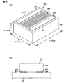
- FIG. 1A is a schematic perspective view showing an external configuration of a chip resistor 10 according to an embodiment of the present invention
- FIG. 1B is a diagram illustrating the chip resistor 10 mounted on a substrate. It is a side view which shows a state.
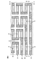
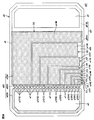
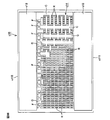
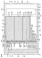
- FIG. 2 is a plan view of the chip resistor 10, showing the arrangement relationship of the first connection electrode 12, the second connection electrode 13, and the resistor network 14 and the configuration of the resistor network 14 in plan view.
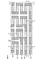
- FIG. 3A is an enlarged plan view illustrating a part of the resistor network 14 shown in FIG.
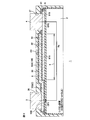
- FIG. 3B is a longitudinal sectional view in the length direction for explaining the configuration of the resistor R in the resistor network 14.
- FIG. 3C is a longitudinal sectional view in the width direction drawn for explaining the configuration of the resistor R in the resistor network 14.
- FIG. 4 is a diagram showing the electrical characteristics of the resistance film line 20 and the conductor film 21 with circuit symbols and electrical circuit diagrams.
- 5A is a partially enlarged plan view of a region including the fuse film F drawn by enlarging a part of the plan view of the chip resistor shown in FIG. 2, and
- FIG. 5B is a plan view of FIG. 2 is a diagram showing a cross-sectional structure taken along line BB in FIG.
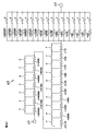
- FIG. 6 shows the arrangement relationship of the connecting conductor film C and the fuse film F connecting the plurality of types of resistance unit bodies in the resistor network 14 shown in FIG.
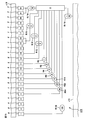
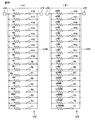
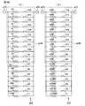
- FIG. 7 is an electric circuit diagram of the resistor network 14.
- FIG. 8 is a plan view of the chip resistor 30, showing the arrangement relationship of the first connection electrode 12, the second connection electrode 13, and the resistor network 14 and the configuration of the resistor network 14 in plan view.
- FIG. 9 shows the arrangement relationship of the connecting conductor film C and the fuse film F connecting the plurality of types of resistance unit bodies in the resistor network 14 shown in FIG. 8, and the connecting conductor film C and the fuse film F connected to the connecting conductor film C and the fuse film F.
- FIG. 10 is an electric circuit diagram of the resistor network 14.
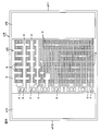
- FIG. 11 is a plan view of a chip capacitor according to an embodiment of the present invention. 12 is a cross-sectional view taken along section line XII-XII in FIG.
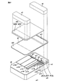
- FIG. 13 is an exploded perspective view showing a part of the chip capacitor separately.
- FIG. 14 is a circuit diagram showing an internal electrical configuration of the chip capacitor.
- FIG. 15 is a plan view for explaining the configuration of a chip capacitor according to another embodiment of the present invention.
- FIG. 16 is an exploded perspective view for explaining the configuration of a chip capacitor according to still another embodiment of the present invention.
- FIG. 10 is an electric circuit diagram of the resistor network 14.
- FIG. 13 is an exploded perspective view showing a part of the chip capacitor separately.
- FIG. 14 is
- FIG. 17 is a schematic sectional view showing an example of the configuration of the external connection electrode that is a feature of the present invention.
- FIG. 18 is a schematic partial sectional view showing another external connection electrode structure applied to the chip resistor 10.
- FIG. 19 is a schematic partial cross-sectional view illustrating a configuration when an external connection electrode according to an embodiment of the present invention is applied to a chip capacitor 1.
- FIG. 20 is a partial longitudinal sectional view showing a configuration example of another external connection electrode applied to the chip capacitor 1.
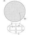
- FIG. 21 is an illustrative view illustrating that a chip resistor is cut out from a semiconductor wafer (silicon wafer).
- FIG. 22A is an illustrative perspective view showing an external configuration of a chip resistor a10 according to an embodiment of the first reference example, and FIG.
- FIG. 22B is a diagram illustrating the chip resistor a10 mounted on a substrate. It is a side view which shows the state made.
- FIG. 23 is a plan view of the chip resistor a10, and shows a positional relationship between the first connection electrode a12, the second connection electrode a13, and the resistance network a14, and a configuration in plan view of the resistance network a14.
- 24A is a plan view illustrating a part of the resistor network a14 illustrated in FIG. 23 in an enlarged manner.
- FIG. 24B is a longitudinal sectional view in the length direction for explaining the configuration of the resistor R in the resistor network a14.
- FIG. 24C is a longitudinal sectional view in the width direction drawn to explain the configuration of the resistor R in the resistor network a14.
- FIG. 25 is a diagram showing the electrical characteristics of the resistance film line a20 and the conductor film a21 with circuit symbols and electrical circuit diagrams.
- 26A is a partially enlarged plan view of a region including the fuse film F drawn by enlarging a part of the plan view of the chip resistor shown in FIG. 23.
- FIG. 26B is a plan view of FIG. 2 is a diagram showing a cross-sectional structure taken along line BB in FIG.
- FIG. 27 shows the arrangement relationship of the connection conductor film C and the fuse film F connecting the plurality of types of resistance unit bodies in the resistance network a14 shown in FIG.
- FIG. 28 is an electric circuit diagram of the resistor network a14.
- FIG. 29 is a plan view of the chip resistor a30, and is a diagram illustrating the arrangement relationship of the first connection electrode a12, the second connection electrode a13, and the resistor network a14, and the configuration of the resistor network a14 in plan view.
- FIG. 30 shows the arrangement relationship of the connection conductor film C and the fuse film F connecting the plurality of types of resistance unit bodies in the resistor network a14 shown in FIG. 29, and the connection conductor film C and the fuse film F connected to the connection conductor film C.
- FIG. 31 is an electric circuit diagram of the resistor network a14.
- FIG. 32 is a plan view of a chip capacitor according to an embodiment of the first reference example.
- FIG. 33 is a cross-sectional view taken along section line XXXIII-XXXIII in FIG.
- FIG. 34 is an exploded perspective view showing a part of the structure of the chip capacitor separately.
- FIG. 35 is a circuit diagram showing an internal electrical configuration of the chip capacitor.
- FIG. 36 is a plan view for explaining a configuration of a chip capacitor according to another embodiment of the first reference example.
- FIG. 37 is an exploded perspective view for explaining a configuration of a chip capacitor according to still another embodiment of the first reference example.
- FIG. 31 is an electric circuit diagram of the resistor network a14.
- FIG. 32 is a plan view of a chip capacitor according to an embodiment of the first reference example.
- FIG. 33 is a cross-sectional view taken along section line XXXIII-XXXIII in FIG.
- FIG. 38 is a diagram for explaining an example of the configuration of the external connection electrode, which is a feature of the first reference example.
- FIG. 38A is a partial plan view of the chip resistor a10, and shows a cut portion BB.
- B is a schematic partial longitudinal sectional view of a cut portion along BB in (A).
- FIG. 39 is an illustrative partial cross-sectional view illustrating a configuration when the external connection electrode according to an embodiment of the first reference example is applied to the chip capacitor a1.
- FIG. 40 is an illustrative view illustrating that the chip resistor is cut out from the semiconductor wafer (silicon wafer).
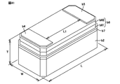
- FIG. 41 is a perspective view of a chip resistor b1 according to an embodiment of the second reference example.
- FIG. 42 is a plan view of a chip resistor b1 according to an embodiment of the second reference example.
- FIG. 43 is a longitudinal sectional view of the chip resistor b1 along XLIII-XLIII in FIG.
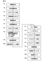
- FIG. 44 is a flowchart showing an example of the manufacturing process of the chip resistor b1.
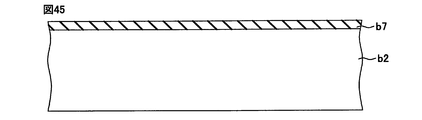
- FIG. 45 is a longitudinal sectional view showing one process of manufacturing the chip resistor b1.
- FIG. 46 is a longitudinal sectional view showing one process of manufacturing the chip resistor b1.
- FIG. 47 is a longitudinal sectional view showing one process of manufacturing the chip resistor b1.
- FIG. 48 is a longitudinal sectional view showing one process of manufacturing the chip resistor b1.
- FIG. 49 is a longitudinal sectional view showing one process of manufacturing the chip resistor b1.
- FIG. 45 is a longitudinal sectional view showing one process of manufacturing the chip resistor b1.
- FIG. 50 is a longitudinal sectional view showing one process of manufacturing the chip resistor b1.
- FIG. 51 is a longitudinal sectional view showing one process of manufacturing the chip resistor b1.
- FIG. 52 is a longitudinal sectional view showing one process of manufacturing the chip resistor b1.
- FIG. 53 is a longitudinal sectional view showing a process of manufacturing the chip resistor b1.
- FIG. 54 is a longitudinal sectional view showing one process of manufacturing the chip resistor b1.
- FIG. 55 is a longitudinal sectional view showing a process of manufacturing the chip resistor b1.
- FIG. 56 is an illustrative view showing one example of a processing step for separating a chip resistor from a substrate.
- FIG. 57 is an illustrative view showing one example of processing steps for separating the chip resistors from the substrate.
- FIG. 58 is an illustrative view showing one example of a processing step for separating a chip resistor from a substrate.
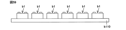
- FIG. 59 is an illustrative view showing one example of a process for separating the chip resistors from the substrate.
- FIG. 60 is a longitudinal sectional view of a chip resistor according to another embodiment of the second reference example.
- FIG. 61 is a longitudinal sectional view of a chip resistor according to still another embodiment of the second reference example.
- FIG. 62 is a plan view of a chip resistor according to still another embodiment of the second reference example.
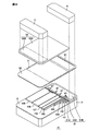
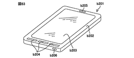
- FIG. 63 is a perspective view illustrating an appearance of a smartphone that is an example of an electronic device in which the chip resistor of the second reference example is used.
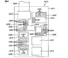
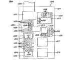
- FIG. 64 is a schematic plan view showing the configuration of the electronic circuit assembly b210 accommodated in the housing b202.
- FIG. 65A is an illustrative perspective view showing an external configuration of a chip resistor c10 according to an embodiment of the third reference example, and
- FIG. 65B is a diagram illustrating the chip resistor c10 mounted on a substrate. It is a side view which shows the state made.
- FIG. 66 is a plan view of the chip resistor c10, and shows a positional relationship between the first connection electrode c12, the second connection electrode c13, and the resistance network c14, and a configuration in plan view of the resistance network c14.
- FIG. 67A is an enlarged plan view of a part of the resistor network c14 shown in FIG.
- FIG. 67B is a longitudinal sectional view in the longitudinal direction drawn for explaining the configuration of the resistor R in the resistor network c14.
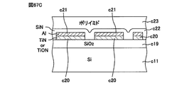
- FIG. 67C is a longitudinal sectional view in the width direction drawn to explain the configuration of the resistor R in the resistor network c14.
- FIG. 68 is a diagram showing the electrical characteristics of the resistance film line c20 and the conductor film c21 with circuit symbols and electrical circuit diagrams.
- 69A is a partially enlarged plan view of a region including the fuse film F drawn by enlarging a part of the plan view of the chip resistor shown in FIG. 66
- FIG. 69B is a plan view of FIG. 2 is a diagram showing a cross-sectional structure taken along line BB in FIG.
- FIG. 70 shows an arrangement relationship of the connection conductor film C and the fuse film F connecting the plurality of types of resistance unit bodies in the resistance network c14 shown in FIG. 66, and the connection conductor film C and the fuse film F connected to the connection conductor film C.
- FIG. 71 is an electric circuit diagram of the resistor network c14.
- FIG. 72 is a plan view of the chip resistor c30, showing the arrangement relationship of the first connection electrode c12, the second connection electrode c13, and the resistance network c14, and the configuration in plan view of the resistance network c14.
- FIG. 73 shows the arrangement relationship of the connection conductor film C and the fuse film F connecting the plurality of types of resistance unit bodies in the resistance network c14 shown in FIG. 72, and the connection conductor film C and the fuse film F connected to the connection conductor film C. It is a figure which shows the connection relation with several types of resistance unit bodies diagrammatically.
- FIG. 71 is an electric circuit diagram of the resistor network c14.
- FIG. 72 is a plan view of the chip resistor c30, showing the arrangement relationship of the first connection electrode c12, the second connection electrode c13, and the resistance network c14, and the configuration in plan view of the resistance network c14.
- FIG. 74 is an electric circuit diagram of the resistor network c14.
- 75A and 75B are electric circuit diagrams showing modifications of the electric circuit shown in FIG.
- FIG. 76 is an electric circuit diagram of a resistor network c14 according to still another embodiment of the third reference example.
- FIG. 77 is an electric circuit diagram showing a configuration example of a resistance network in a chip resistor displaying a specific resistance value.
- FIG. 78 is an illustrative plan view for explaining a main structure of a chip resistor 90 according to still another embodiment of the third reference example.
- FIG. 79 is a flowchart showing an example of the manufacturing process of the chip resistor c10.
- FIG. 80 is a schematic cross-sectional view showing a fusing process of the fuse film F and a passivation film c22 and a resin film c23 formed thereafter.
- FIG. 81 is an illustrative view showing a processing step of separating the chip resistors from the substrate.
- FIG. 82 is an illustrative view illustrating that the chip resistor is cut out from the substrate.
- FIG. 83 is a perspective view illustrating an appearance of a smartphone that is an example of an electronic device in which the chip resistor of the third reference example is used.
- FIG. 84 is a schematic plan view showing the configuration of the electronic circuit assembly c210 housed in the housing c202.
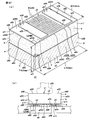
- FIG. 85A is a schematic perspective view for explaining the configuration of the chip resistor according to the embodiment of the fourth reference example.
- FIG. 85B is a schematic cross-sectional view of the circuit assembly in a state where the chip resistor is mounted on the mounting substrate, cut along the longitudinal direction of the chip resistor.
- FIG. 85C is a schematic cross-sectional view of the circuit assembly in a state where the chip resistor is mounted on the mounting substrate, cut along the short direction of the chip resistor.
- FIG. 85D is a schematic plan view of the chip resistor mounted on the mounting substrate as viewed from the element formation surface side.
- FIG. 85E is a schematic cross-sectional view of the circuit assembly in a state where the chip resistor is mounted on the multilayer substrate, cut along the longitudinal direction of the chip resistor.
- FIG. 85B is a schematic cross-sectional view of the circuit assembly in a state where the chip resistor is mounted on the mounting substrate, cut along the longitudinal direction of the chip resistor.
- FIG. 85C is
- FIG. 86 is a plan view of the chip resistor, showing the arrangement relationship between the first connection electrode, the second connection electrode and the element, and the configuration of the element in plan view.
- FIG. 87A is a plan view illustrating a part of the element shown in FIG. 86 in an enlarged manner.
- FIG. 87B is a longitudinal sectional view in the length direction taken along the line BB of FIG. 87A, which is drawn for explaining the configuration of the resistor in the element.
- FIG. 87C is a longitudinal sectional view in the width direction taken along the line CC of FIG. 87A drawn to explain the configuration of the resistor in the element.
- FIG. 88 is a diagram showing the electrical characteristics of the resistor film line and the wiring film with circuit symbols and electrical circuit diagrams.
- FIG. 90 is an electric circuit diagram of an element according to the embodiment of the fourth reference example.
- FIG. 91 is an electric circuit diagram of an element according to another embodiment of the fourth reference example.
- FIG. 92 is an electric circuit diagram of an element according to still another embodiment of the fourth reference example.
- FIG. 93 is a schematic cross-sectional view of a chip resistor.
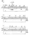
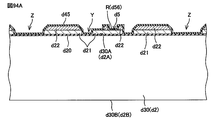
- 94A is a schematic cross-sectional view showing a method for manufacturing the chip resistor shown in FIG. 93.
- FIG. FIG. 94B is an illustrative sectional view showing a step subsequent to FIG. 94A.
- FIG. 94C is an illustrative sectional view showing a step subsequent to FIG. 94B.
- FIG. 94D is an illustrative sectional view showing a step subsequent to FIG. 94C.
- FIG. 94E is an illustrative sectional view showing a step subsequent to FIG. 94D.
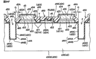
- FIG. 94F is an illustrative sectional view showing a step subsequent to FIG. 94E.
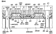
- FIG. 94G is an illustrative sectional view showing a step subsequent to FIG. 94F.
- FIG. 95 is a schematic plan view of a part of a resist pattern used for forming a groove in the step of FIG. 94B.
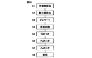
- FIG. 96 is a diagram for explaining a manufacturing process of the first connection electrode and the second connection electrode.
- FIG. 97 is a plan view of a chip capacitor according to another embodiment of the fourth reference example.
- 98 is a cross-sectional view taken along section line XCVIII-XCVIII in FIG.
- FIG. 99 is an exploded perspective view showing a part of the structure of the chip capacitor separately.
- FIG. 100 is a circuit diagram showing an internal electrical configuration of the chip capacitor.
- FIG. 101 is a plan view of a chip diode according to still another embodiment of the fourth reference example.
- FIG. 102 is a cross-sectional view taken along section line CII-CII in FIG. 103 is a cross-sectional view taken along section line CIII-CIII in FIG.
- FIG. 104 is a plan view showing the structure of the element formation surface of the substrate by removing the cathode and anode electrodes and the structure formed thereon from the chip diode.
- FIG. 105 is a perspective view illustrating an appearance of a smartphone that is an example of an electronic device in which the chip component of the fourth reference example is used.
- FIG. 106 is a schematic plan view showing the configuration of the circuit assembly housed in the housing of the smartphone.
- FIG. 107 (a) is a schematic perspective view for explaining the configuration of the chip resistor according to the embodiment of the fifth reference example, and FIG.
- FIG. 107 (b) is a diagram illustrating the chip resistor mounted on the mounting substrate. It is typical sectional drawing which shows the state made.
- FIG. 108 is a plan view of the chip resistor, showing the arrangement relationship of the first connection electrode, the second connection electrode and the element, and the configuration of the element in plan view.
- FIG. 109A is an enlarged plan view of a part of the element shown in FIG.
- FIG. 109B is a longitudinal sectional view in the length direction taken along the line BB of FIG. 109A, which is drawn for explaining the configuration of the resistor in the element.
- FIG. 109C is a longitudinal sectional view in the width direction along CC of FIG. 109A drawn to explain the structure of the resistor in the element.
- FIG. 108 is a plan view of the chip resistor, showing the arrangement relationship of the first connection electrode, the second connection electrode and the element, and the configuration of the element in plan view.
- FIG. 109A is an enlarged plan view of a part of the
- FIG. 110 is a diagram showing the electrical characteristics of the resistor film line and the wiring film with circuit symbols and electrical circuit diagrams.
- FIG. 111A is a partially enlarged plan view of a region including a fuse drawn by enlarging a part of the plan view of the chip resistor shown in FIG. 108
- FIG. 111B is a plan view of FIG. 111A. It is a figure which shows the cross-sectional structure which follows BB.
- FIG. 112 is an electric circuit diagram of an element according to an embodiment of the fifth reference example.
- FIG. 113 is an electric circuit diagram of an element according to another embodiment of the fifth reference example.
- FIG. 114 is an electric circuit diagram of an element according to still another embodiment of the fifth reference example.
- FIG. 112 is an electric circuit diagram of an element according to an embodiment of the fifth reference example.
- FIG. 113 is an electric circuit diagram of an element according to another embodiment of the fifth reference example.
- FIG. 114 is an electric circuit diagram of an element according to still another
- FIG. 115 is a schematic cross-sectional view of a chip resistor.
- 116A is a schematic cross-sectional view showing a method for manufacturing the chip resistor shown in FIG. 115.
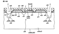
- FIG. 116B is a schematic sectional view showing a step subsequent to FIG. 116A.
- FIG. 116C is an illustrative sectional view showing a step subsequent to FIG. 116B.
- FIG. 116D is an illustrative sectional view showing a step subsequent to FIG. 116C.
- FIG. 116E is an illustrative sectional view showing a step subsequent to FIG. 116D.
- FIG. 116F is a schematic sectional view showing a step subsequent to FIG. 116E.
- FIG. 116G is an illustrative sectional view showing a step subsequent to FIG. 116F.
- FIG. 116H is an illustrative sectional view showing a step subsequent to FIG. 116G.
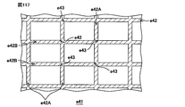
- FIG. 117 is a schematic plan view of a part of the resist pattern used for forming the first groove in the step of FIG. 116B.
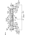
- FIG. 118 is a diagram for explaining a manufacturing process of the first connection electrode and the second connection electrode.
- FIG. 119 is a schematic diagram for explaining how the completed chip resistor is accommodated in the embossed carrier tape.
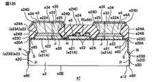
- FIG. 120 is a schematic cross-sectional view of a chip resistor according to a first modification of the fifth reference example.
- FIG. 120 is a schematic cross-sectional view of a chip resistor according to a first modification of the fifth reference example.
- FIG. 121 is a schematic cross-sectional view of a chip resistor according to a second modification example of the fifth reference example.
- FIG. 122 is a schematic cross-sectional view of a chip resistor according to a third modification example of the fifth reference example.
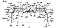
- FIG. 123 is a schematic cross-sectional view of a chip resistor according to a fourth modification example of the fifth reference example.
- FIG. 124 is a schematic cross-sectional view of a chip resistor according to a fifth modification example of the fifth reference example.
- FIG. 125 is a plan view of a chip capacitor according to another embodiment of the fifth reference example.
- 126 is a sectional view taken along section line CXXVI-CXXVI in FIG. FIG.
- FIG. 127 is an exploded perspective view showing a part of the structure of the chip capacitor separately.
- FIG. 128 is a circuit diagram showing an internal electrical configuration of the chip capacitor.
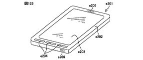
- FIG. 129 is a perspective view illustrating an appearance of a smartphone that is an example of an electronic device in which the chip component of the fifth reference example is used.
- FIG. 130 is a schematic plan view showing the configuration of the electronic circuit assembly housed inside the housing of the smartphone.
- FIG. 131A is a schematic perspective view for explaining the configuration of the chip resistor according to the embodiment of the sixth reference example, and
- FIG. 131B is a diagram illustrating the chip resistor mounted on the mounting substrate. It is typical sectional drawing which shows the state made.
- FIG. 132 is a plan view of the chip resistor, showing the arrangement relationship between the first connection electrode, the second connection electrode and the element, and the configuration of the element in plan view.
- FIG. 133A is a plan view illustrating a part of the element shown in FIG. 132 in an enlarged manner.
- FIG. 133B is a longitudinal sectional view in the length direction taken along the line BB of FIG. 133A, which is drawn for explaining the configuration of the resistor in the element.
- FIG. 133C is a longitudinal sectional view in the width direction along CC of FIG. 133A drawn for explaining the configuration of the resistor in the element.
- FIG. 134 is a diagram showing the electrical characteristics of the resistor film line and the wiring film with circuit symbols and electrical circuit diagrams.
- FIG. 135 (a) is a partially enlarged plan view of a region including a fuse drawn by enlarging a part of the plan view of the chip resistor shown in FIG. 132
- FIG. 135 (b) is a diagram of FIG. 135 (a). It is a figure which shows the cross-sectional structure which follows BB.
- FIG. 136 is an electric circuit diagram of an element according to an embodiment of the sixth reference example.
- FIG. 137 is an electric circuit diagram of an element according to another embodiment of the sixth reference example.
- FIG. 138 is an electric circuit diagram of an element according to still another embodiment of the sixth reference example.
- FIG. 139 is a schematic cross-sectional view of a chip resistor.
- FIG. 140A is a schematic sectional view showing a method for manufacturing the chip resistor shown in FIG. 139.
- FIG. FIG. 140B is a schematic sectional view showing a step subsequent to FIG. 140A.
- FIG. 140C is an illustrative sectional view showing a step subsequent to FIG. 140B.
- FIG. 140D is an illustrative sectional view showing a step subsequent to FIG. 140C.
- FIG. 140E is an illustrative sectional view showing a step subsequent to FIG. 140D.
- FIG. 140F is a schematic sectional view showing a step subsequent to FIG. 140E.
- FIG. 140G is an illustrative sectional view showing a step subsequent to FIG. 140F.
- FIG. 140H is an illustrative sectional view showing a step subsequent to FIG. 140G.
- FIG. 141 is a schematic plan view of a part of the resist pattern used for forming the first groove in the step of FIG. 140B.
- FIG. 142 is a diagram for explaining a manufacturing process of the first connection electrode and the second connection electrode.
- FIG. 143 is a schematic diagram for explaining how the completed chip resistor is accommodated in the embossed carrier tape.
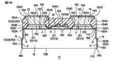
- FIG. 144 is a schematic cross-sectional view of a chip resistor according to a first modification example of the sixth reference example.
- FIG. 145 is a schematic cross-sectional view of a chip resistor according to a second modification example of the sixth reference example.
- FIG. 144 is a schematic cross-sectional view of a chip resistor according to a first modification example of the sixth reference example.
- FIG. 146 is a schematic cross-sectional view of a chip resistor according to a third modification example of the sixth reference example.
- FIG. 147 is a schematic cross-sectional view of a chip resistor according to a fourth modification example of the sixth reference example.
- FIG. 148 is a schematic cross-sectional view of a chip resistor according to a fifth modification example of the sixth reference example.
- FIG. 149 is a plan view of a chip capacitor according to another embodiment of the sixth reference example.
- 150 is a cross-sectional view taken along section line CL-CL in FIG.
- FIG. 151 is an exploded perspective view showing a part of the structure of the chip capacitor separately.
- FIG. 152 is a circuit diagram showing an internal electrical configuration of the chip capacitor.
- FIG. 152 is a circuit diagram showing an internal electrical configuration of the chip capacitor.
- FIG. 153 is a perspective view illustrating an appearance of a smartphone that is an example of an electronic device in which the chip component of the sixth reference example is used.
- FIG. 154 is an illustrative plan view showing the configuration of the electronic circuit assembly housed inside the housing of the smartphone.
- FIG. 155 (A) is an illustrative perspective view showing an external configuration of a chip resistor g10 according to an embodiment of the seventh reference example, and FIG. 155 (B) shows a chip resistor g10 mounted on a substrate. It is a side view which shows the state made.
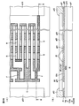
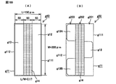
- FIG. 156 is a plan view of the chip resistor g10, and shows a positional relationship between the first connection electrode g12, the second connection electrode g13, and the resistor network g14, and a configuration in plan view of the resistor network g14.
- FIG. 157A is an enlarged plan view of a part of the resistor network g14 shown in FIG.
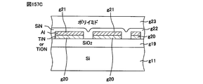
- FIG. 157B is a longitudinal sectional view in the length direction drawn for explaining the configuration of the resistor R in the resistor network g14.
- FIG. 157C is a longitudinal sectional view in the width direction drawn for explaining the configuration of the resistor R in the resistor network g14.
- FIG. 158 is a diagram showing the electrical characteristics of the resistive film line g20 and the conductive film g21 with circuit symbols and electrical circuit diagrams.
- FIG. 159 (A) is a partially enlarged plan view of a region including the fuse F drawn by enlarging a part of the plan view of the chip resistor shown in FIG. 156
- FIG. 159 (B) is a plan view of FIG. It is a figure which shows the cross-sectional structure in alignment with BB.
- FIG. 160 shows the arrangement relationship of the connection conductor film C and the fuse F connecting the plurality of types of resistance unit bodies in the resistance network g14 shown in FIG. 156, and the connection relation between the connection conductor film C and the fuse film F.
- FIG. 161 is an electric circuit diagram of the resistor network g14.
- FIG. 162 is a plan view of the chip resistor g30, and shows a positional relationship between the first connection electrode g12, the second connection electrode g13, and the resistor network g14, and a configuration in plan view of the resistor network g14.
- FIG. 163 shows the arrangement relationship of the connection conductor film C and the fuse F connecting the plurality of types of resistance unit bodies in the resistance network g14 shown in FIG. 162, and the plurality of types connected to the connection conductor film C and the fuse F. It is a figure which shows diagrammatically the connection relation with the resistance unit body.
- FIG. 161 is an electric circuit diagram of the resistor network g14.
- FIG. 162 is a plan view of the chip resistor g30, and shows a positional relationship between the first connection electrode g12, the second connection electrode g13, and the resistor network g14, and a configuration in plan view of the resistor network
- FIG. 164 is an electric circuit diagram of the resistor network g14.
- FIGS. 165A and 165B are electric circuit diagrams illustrating modifications of the electric circuit illustrated in FIG. 164.
- FIG. 166 is an electrical circuit diagram of a resistor network g14 according to still another embodiment of the seventh reference example.
- FIG. 167 is an electric circuit diagram showing a configuration example of a resistance network in a chip resistor displaying a specific resistance value.
- FIG. 168 is an illustrative plan view for explaining a main structure of a chip resistor g90 according to still another embodiment of the seventh reference example.
- FIG. 169 is a plan view showing an arrangement configuration (layout) of electrodes of a chip resistor according to another embodiment of the seventh reference example.
- FIG. 170 is a flowchart showing an example of the manufacturing process of the chip resistor g10.
- FIG. 171 is a schematic cross-sectional view showing the fusing process of the fuse film F and the passivation film g22 and the resin film g23 formed thereafter.
- FIG. 172 is an illustrative view showing a process step of separating the chip resistors from the substrate.
- FIG. 173 is a plan view of a chip capacitor g301 according to another embodiment of the seventh reference example.
- FIG. 174 is a cross-sectional view of the chip capacitor g301 and is a cross-sectional view taken along the cross-sectional line CLXXIV-CLXXIV of FIG. 173.
- FIG. 175 is a circuit diagram showing an internal electrical configuration of the chip capacitor g301.
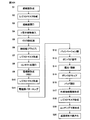
- FIG. 176 is a flowchart for explaining an example of the manufacturing process of the chip capacitor g301.
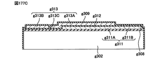
- FIG. 177A is a diagram illustrating one process of manufacturing the chip capacitor g301.
- FIG. 177B is a diagram illustrating one process of manufacturing the chip capacitor g301.
- FIG. 177C is a diagram illustrating one process of manufacturing the chip capacitor g301. It is an illustration top view for explaining the principal part structure of chip resistor g90 concerning other embodiments of the 7th reference example.
- FIG. 178 is a perspective view of a chip diode g401 according to another embodiment of the seventh reference example.
- FIG. 179 is a plan view of a chip diode g401 according to another embodiment of the seventh reference example.
- 180 is a cross-sectional view taken along the line CLXXX-CLXXX in FIG.
- FIG. 181 is a cross-sectional view taken along CLXXXI-CLXXXI in FIG.
- FIG. 182 is a plan view showing the structure of the surface (element formation surface g402a) of the semiconductor substrate g402 by removing the cathode electrode g403 and the anode electrode g404 and the structure formed thereon.
- FIG. 183 is an electric circuit diagram showing the internal electrical structure of the chip diode g401.
- FIG. 184 is a process diagram for explaining an example of the manufacturing process of the chip diode g401.
- FIG. 185A is a cross-sectional view showing a configuration in the middle of the manufacturing process of FIG. 184, and shows a cut surface corresponding to FIG.
- FIG. 185B is a cross-sectional view showing the configuration in the middle of the manufacturing process of FIG. 184 and shows a cut surface corresponding to FIG. 180.
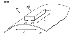
- FIG. 186 is an illustrative perspective view showing a configuration example of a circuit assembly according to an embodiment of a seventh reference example.
- FIG. 187 is a perspective view illustrating an appearance of a smartphone that is an example of an electronic device in which the chip resistor of the seventh reference example is used.
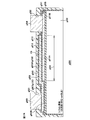
- FIG. 188 is a schematic plan view showing the configuration of the electronic circuit assembly g210 accommodated in the housing g202.
- FIG. 1A is a schematic perspective view showing an external configuration of a chip resistor 10 according to an embodiment of the present invention
- FIG. 1B is a diagram illustrating the chip resistor 10 mounted on a substrate. It is a side view which shows a state.
- a chip resistor 10 according to an embodiment of the present invention includes a first connection electrode 12, a second connection electrode 13, and a resistor network 14 formed on a substrate 11. It has.
- the substrate 11 has a substantially rectangular parallelepiped shape in plan view.
- the length L in the long side direction is 0.3 mm
- the width W in the short side direction is 0.15 mm
- the thickness T is about 0.1 mm. It is a very small chip.
- the substrate 11 may have a rounded corner shape with chamfered corners in plan view.
- the substrate can be formed of, for example, silicon, glass, ceramic or the like. In the following embodiment, a case where the substrate 11 is a silicon substrate will be described as an example. *
- the chip resistor 10 As shown in FIG. 21, in the chip resistor 10, a large number of chip resistors 10 are formed in a lattice shape on a semiconductor wafer (silicon wafer), and the semiconductor wafer (silicon wafer) is cut to obtain individual chip resistors. It is obtained by separating into 10.
- the first connection electrode 12 is a rectangular electrode that is provided along one short side 111 of the silicon substrate 11 and is long in the direction of the short side 111.
- the second connection electrode 13 is a rectangular electrode extending in the direction of the short side 112 provided along the other short side 112 on the silicon substrate 11.
- the resistance network 14 is provided in a central region (circuit formation surface or element formation surface) sandwiched between the first connection electrode 12 and the second connection electrode 13 on the silicon substrate 11.
- the resistor network 14 is electrically connected to the first connection electrode 12, and the other end side of the resistor network 14 is electrically connected to the second connection electrode 13.
- the first connection electrode 12, the second connection electrode 13, and the resistance network 14 can be provided on the silicon substrate 11 by using a semiconductor manufacturing process.
- the discrete chip resistor 10 can be manufactured using an apparatus and equipment for manufacturing a semiconductor device.
- the resistance network 14 having a fine and accurate layout pattern can be formed by using a photolithography process described later.
- the first connection electrode 12 and the second connection electrode 13 each function as an external connection electrode.
- the first connection electrode 12 and the second connection electrode 13 are respectively connected to a circuit (not shown) of the circuit board 15. ) And solder and are electrically and mechanically connected.
- the first connection electrode 12 and the second connection electrode 13 that function as external connection electrodes are made of gold (Au) or copper (Cu), and the surface that is the connection end is preliminarily soldered. A layer is provided. For this reason, there is no need for solder printing at the time of mounting, and the chip resistor is easy to mount. *
- FIG. 2 is a plan view of the chip resistor 10, showing the arrangement relationship of the first connection electrode 12, the second connection electrode 13 and the resistor network 14 and the configuration (layout pattern) of the resistor network 14 in plan view.
- the chip resistor 10 includes a first connection electrode 12 having a substantially rectangular shape in plan view arranged so that a long side is along one short side 111 of the upper surface of the silicon substrate, and the other short side of the upper surface of the silicon substrate.
- the second connection electrode 13 having a substantially rectangular shape in plan view arranged so that the long side extends along the side 112, and a resistance network provided in a rectangular region in plan view between the first connection electrode 12 and the second connection electrode 13 14 and so on.
- the resistor network 14 includes a plurality of unit resistors R (equal to the row direction (longitudinal direction of the silicon substrate) in the example of FIG. 2) having the same resistance value arranged in a matrix on the silicon substrate 11.
- Unit resistors R are arranged, and 44 unit resistors R are arranged along the column direction (the width direction of the silicon substrate), and the structure includes a total of 352 unit resistors R).
- a predetermined number of 1 to 64 of the large number of unit resistors R is electrically connected (by a wiring film formed of a conductor), and a plurality of unit resistors R corresponding to the number of unit resistors R connected.
- Various resistance circuits are formed.
- a plurality of types of formed resistance circuits are connected in a predetermined manner by a conductor film C (a wiring film formed of a conductor). *
- a plurality of fuse films F (wiring films formed of conductors) that can be blown in order to electrically incorporate the resistor circuit into the resistor network 14 or to be electrically separated from the resistor network 14 are provided. ing.
- the plurality of fuse films F are arranged along the inner side of the second connection electrode 13 so that the arrangement region is linear. More specifically, the plurality of fuse films F and the connecting conductor film C are arranged so as to be adjacent to each other, and arranged in a straight line.
- FIG. 3A is an enlarged plan view of a part of the resistor network 14 shown in FIG. 2, and FIGS. 3B and 3C are diagrams for explaining the structure of the unit resistor R in the resistor network 14, respectively. It is the longitudinal cross-sectional view of the drawn length direction, and the longitudinal cross-sectional view of the width direction. A configuration of the unit resistor R will be described with reference to FIGS. 3A, 3B, and 3C.
- An insulating layer (SiO 2 ) 19 is formed on the upper surface of a silicon substrate 11 as a substrate, and a resistor film 20 is disposed on the insulating layer 19.
- the resistor film 20 is formed of TiN, TiON, or TiSiON.
- the resistor film 20 is a plurality of resistor films (hereinafter referred to as “resistor film lines”) extending linearly in parallel between the first connection electrode 12 and the second connection electrode 13.
- the body membrane line 20 may be cut at a predetermined position in the line direction.
- An aluminum film as a conductor film piece 21 is laminated on the resistor film line 20.
- Each conductor film piece 21 is laminated on the resistor film line 20 with a predetermined interval R in the line direction.
- each of the resistor film lines 20 in the region of the predetermined interval R forms a unit resistor R having a constant resistance value r.
- the resistor film line 20 is short-circuited by the conductor film pieces 21. Therefore, a resistor circuit is formed which is formed by connecting in series the unit resistors R of the resistor r shown in FIG. *
- the resistor network shown in FIG. 3A constitutes the resistor circuit shown in FIG. Yes. 3B and 3C
- reference numeral 11 is a silicon substrate
- 19 is a silicon dioxide SiO2 layer as an insulating layer
- 20 is a TiN, TiON or TiSiON resistor formed on the insulating layer 19.
- a film, 21 is an aluminum (Al) wiring film
- 22 is a SiN film as a protective film
- 23 is a polyimide layer as a protective layer.
- the unit resistor R included in the resistor network 14 formed on the silicon substrate 11 is laminated on the resistor film line 20 and the resistor film line 20 with a certain interval in the line direction.
- a plurality of conductor film pieces 21 are formed, and a resistor film line 20 at a constant interval R where the conductor film pieces 21 are not laminated constitutes one unit resistor R.
- the resistor film lines 20 constituting the unit resistor R are all equal in shape and size. Therefore, based on the characteristic that the same-shaped and large-sized resistor films formed on the substrate have substantially the same value, a large number of unit resistors R arranged in a matrix on the silicon substrate 11 have the same resistance value. have. *
- the conductor film piece 21 laminated on the resistor film line 20 forms a unit resistor R, and also serves as a connection wiring film for connecting a plurality of unit resistors R to form a resistor circuit.
- Plays. 5A is a partially enlarged plan view of a region including the fuse film F drawn by enlarging a part of the plan view of the chip resistor 10 shown in FIG. 2, and FIG. 5B is a plan view of FIG. It is a figure which shows the cross-sectional structure which follows BB of A). *
- the fuse film F is also formed of the wiring film 21 laminated on the resistor film 20. That is, it is formed of aluminum (Al) which is the same metal material as the conductor film piece 21 in the same layer as the conductor film piece 21 laminated on the resistor film line 20 forming the unit resistor R. As described above, the conductor film piece 21 is also used as a connecting conductor film C for electrically connecting a plurality of unit resistors R in order to form a resistance circuit. *
- a wiring film for forming the unit resistor R, a connecting wiring film for forming a resistor circuit, and a connecting wiring film for forming the resistor network 14 are used.
- the fuse film, and the wiring film for connecting the resistor network 14 to the first connection electrode 12 and the second connection electrode 13 are made of the same metal material (for example, aluminum), and the same manufacturing process (for example, sputtering and photo). Lithographic process). Thereby, the manufacturing process of the chip resistor 10 is simplified, and various wiring films can be simultaneously formed using a common mask. Furthermore, the alignment with the resistor film 20 is also improved. *
- FIG. 6 shows the arrangement relationship of the connecting conductor film C and the fuse film F for connecting a plurality of types of resistor circuits in the resistor network 14 shown in FIG. 2, and the connecting conductor film C and the plurality of fuse films F connected to the fuse film F. It is a figure which shows the connection relation with the resistance circuit of a kind schematically. Referring to FIG. 6, one end of a reference resistor circuit R8 included in the resistor network 14 is connected to the first connection electrode 12.
- the reference resistor circuit R8 is composed of eight unit resistors R connected in series, and the other end is connected to the fuse film F1. *
- the fuse film F1 and the connecting conductor film C2 include 6 One end and the other end of a resistor circuit R64 composed of four unit resistors R connected in series are connected. One end and the other end of a resistor circuit R32 including 32 unit resistors R connected in series are connected to the connecting conductor film C2 and the fuse film F4. One end and the other end of a resistor circuit body R32 formed of a series connection of 32 unit resistors R are connected to the fuse film F4 and the connecting conductor film C5.
- resistor circuit R16 composed of 16 unit resistors R connected in series are connected to the connecting conductor film C5 and the fuse film F6.
- resistor circuit R8 composed of eight unit resistors R connected in series are connected to the fuse film F7 and the connecting conductor film C9.
- the connecting conductor film C9 and the fuse film F10 are connected to one end and the other end of a resistor circuit R4 composed of four unit resistors R connected in series.
- resistor circuit R2 formed of a series connection of two unit resistors R are connected to the fuse film F11 and the connecting conductor film C12.
- resistor circuit body R1 including one unit resistor R are connected to the connecting conductor film C12 and the fuse film F13.
- resistance circuit R / 2 composed of two unit resistors R connected in parallel are connected to the fuse film F13 and the connecting conductor film C15.
- a resistance circuit R / 4 composed of four unit resistors R connected in parallel are connected to the connecting conductor film C15 and the fuse film F16.
- One end and the other end of a resistor circuit R / 8 composed of eight unit resistors R connected in parallel are connected to the fuse film F16 and the connecting conductor film C18.
- One end and the other end of a resistor circuit R / 16 composed of 16 unit resistors R connected in parallel are connected to the connecting conductor film C18 and the fuse film F19.
- a resistor circuit R / 32 composed of 32 unit resistors R connected in parallel is connected to the fuse film F19 and the connecting conductor film C22.
- the plurality of fuse films F and the connecting conductor film C are respectively a fuse film F1, a connecting conductor film C2, a fuse film F3, a fuse film F4, a connecting conductor film C5, a fuse film F6, a fuse film F7, and a connecting conductor.
- Film C8 connecting conductor film C9, fuse film F10, fuse film F11, connecting conductor film C12, fuse film F13, fuse film F14, connecting conductor film C15, fuse film F16, fuse film F17, connecting conductor film C18
- the fuse film F19, the fuse film F20, the connecting conductor film C21, and the connecting conductor film C22 are arranged in a straight line and connected in series. When each fuse film F is melted, the electrical connection with the connection conductor film C adjacently connected to the fuse film F is cut off.
- the resistance network 14 is a reference composed of a series connection of eight unit resistors R provided between the first connection electrode 12 and the second connection electrode 13.
- a resistance circuit of the resistance circuit R8 resistance value 8r
- the fuse films F are connected in parallel to the plurality of types of resistor circuits other than the reference resistor circuit R8, and the plurality of types of resistor circuits are short-circuited by the fuse films F. That is, 12 types of 13 resistor circuits R64 to R / 32 are connected in series to the reference resistor circuit R8, but each resistor circuit is short-circuited by the fuse film F connected in parallel. From an electrical viewpoint, each resistance circuit is not incorporated in the resistance network 14. *
- the chip resistor 10 selectively fuses the fuse film F with, for example, laser light according to a required resistance value.
- the resistor circuit in which the fuse films F connected in parallel are melted is incorporated into the resistor network 14. Therefore, the entire resistance value of the resistance network 14 can be a resistance network having a resistance value in which resistance circuits corresponding to the blown fuse film F are connected in series.
- the chip resistor 10 selectively blows a fuse film provided corresponding to a plurality of types of resistance circuits, thereby providing a plurality of types of resistance circuits (for example, F1, F4,.
- a series connection of resistance circuits R64, R32, and R1) can be incorporated into the resistance network. Since the resistance values of the plurality of types of resistance circuits are determined, the resistance value of the resistance network 14 is digitally adjusted so that the chip resistor 10 having the required resistance value is obtained. Can do. *
- the plurality of types of resistor circuits have unit resistors R having equal resistance values in series of 1, 2, 4, 8, 16, 32, and 64, in a geometric sequence.
- a plurality of types of series resistor circuits connected by increasing the number of unit resistors R and two, four, eight, sixteen, and thirty-two unit resistors R having the same resistance value in parallel
- a plurality of types of parallel resistance circuits are provided which are connected by increasing the number of unit resistors R in a sequence. These are connected in series while being short-circuited by the fuse film F. Therefore, by selectively fusing the fuse film F, the resistance value of the entire resistor network 14 can be set to an arbitrary resistance value within a wide range from a small resistance value to a large resistance value.
- FIG. 8 is a plan view of a chip resistor 30 according to another embodiment of the present invention.
- the arrangement relationship of the first connection electrode 12, the second connection electrode 13, and the resistor network 4 and the plan view of the resistor network 14 are shown.
- the configuration of is shown.
- the difference between the chip resistor 30 and the chip resistor 10 described above is the connection mode of the unit resistors R in the resistor network 14. *
- the resistor network 14 of the chip resistor 30 includes a large number of unit resistors R having the same resistance value arranged in a matrix on the silicon substrate (in the configuration of FIG. 8 unit resistors R are arrayed along the direction), 44 unit resistors R are arrayed along the column direction (the width direction of the silicon substrate), and a total of 352 unit resistors R are included. )have.
- a predetermined number of 1 to 128 of the large number of unit resistors R are electrically connected to form a plurality of types of resistor circuits.
- the formed plurality of types of resistance circuits are connected in parallel by a conductor film and a fuse film F as network connection means.
- the plurality of fuse films F are arranged along the inner side of the second connection electrode 13 so that the arrangement region is linear. When the fuse film F is melted, a resistance circuit connected to the fuse film is formed. In this configuration, the resistor network 14 is electrically separated.
- FIG. 9 illustrates the connection mode of the plurality of types of resistor circuits in the resistor network shown in FIG. 8, the arrangement relationship of the fuse films F connecting them, and the connection relationship of the plurality of types of resistor circuits connected to the fuse film F.
- a reference resistor circuit R / 16 included in the resistor network 14 is connected to the first connection electrode 12.
- the reference resistance circuit R / 16 is composed of 16 unit resistors R connected in parallel, and the other end is connected to a connection conductor film C to which the remaining resistance circuit is connected.
- the fuse film F1 and the connecting conductor film C are connected to one end and the other end of a resistor circuit R128 formed of 128 unit resistors R connected in series.
- resistor circuit R64 composed of 64 unit resistors R connected in series are connected to the fuse film F5 and the connecting conductor film C.
- resistor circuit R32 formed of a series connection of 32 unit resistors R are connected to the resistor film F6 and the connecting conductor film C.
- resistor circuit R16 composed of 16 unit resistors R connected in series are connected to the fuse film F7 and the connecting conductor film C.
- a resistor circuit R8 formed of a series connection of eight unit resistors R are connected to the fuse film F8 and the connecting conductor film C.
- the fuse film F9 and the connecting conductor film C are connected to one end and the other end of a resistor circuit R4 formed by connecting four unit resistors R in series.
- the fuse film F10 and the connecting conductor film C are connected to one end and the other end of a resistor circuit R2 formed by connecting two unit resistors R in series.
- One end and the other end of a resistor circuit R1 formed by connecting one unit resistor R in series are connected to the fuse film F11 and the connecting conductor film C.
- the fuse film F12 and the connecting conductor film C are connected to one end and the other end of a resistance circuit R / 2 formed by connecting two unit resistors R in parallel.
- the fuse film F13 and the connecting conductor film C are connected to one end and the other end of a resistor circuit R / 4 formed of four unit resistors R connected in parallel.
- the fuse films F14, F15, and F16 are electrically connected, and the fuse films F14, F15, and F16 and the connection conductor C are connected to a resistor circuit R / 8 that includes eight unit resistors R connected in parallel. Are connected at one end and the other end.
- the fuse films F17, F18, F19, F20, and F21 are electrically connected, and the fuse films F17 to F21 and the connecting conductor film C have a resistance circuit formed by parallel connection of 16 unit resistors R. One end and the other end of R / 16 are connected. *
- the fuse film F includes 21 fuse films F 1 to F 21, all of which are connected to the second connection electrode 13. With this configuration, when any one of the fuse films F to which one end of the resistor circuit is connected is melted, the resistor circuit having one end connected to the fuse film F is electrically disconnected from the resistor network 14. . *
- FIG. 9 The configuration of FIG. 9, that is, the configuration of the resistor network 14 provided in the chip resistor 30 is shown in an electric circuit diagram as shown in FIG. 10.
- the resistance network 14 includes a reference resistance circuit R / 16, 12 types of resistance circuits R / 16, between the first connection electrode 14 and the second connection electrode 13.
- a series connection circuit is formed with a parallel connection circuit of R / 8, R / 4, R / 2, R1, R2, R4, R8, R16, R32, R64, and R128. *
- a fuse film F is connected in series to each of 12 types of resistance circuits other than the reference resistance circuit R / 16. Therefore, in the chip resistor 30 having this resistance network 14, if the fuse film F is selectively blown by, for example, laser light according to the required resistance value, the resistance corresponding to the blown fuse film F is obtained.
- the circuit resistor circuit in which the fuse film F is connected in series
- the resistance value of the chip resistor 10 can be adjusted.
- the chip resistor 30 also electrically disconnects the plurality of types of resistor circuits from the resistor circuit network by selectively fusing fuse films provided corresponding to the plurality of types of resistor circuits. Can be separated. Since the resistance values of the plurality of types of resistance circuits are respectively determined, the resistance value of the resistance network 14 is digitally adjusted so that the chip resistor 30 having the required resistance value is obtained. Can do. *
- the plurality of types of resistor circuits have unit resistors R having the same resistance value in series of 1, 2, 4, 8, 16, 32, 64, and 128, in a geometric sequence.
- the number of unit resistors R is increased and connected in series, as well as two, four, eight, and sixteen unit resistances R having the same resistance value in parallel.
- a plurality of types of parallel resistance circuits connected with an increased number of unit resistors R Therefore, by selectively fusing the fuse film F, the resistance value of the entire resistance network 14 can be set to an arbitrary resistance value in a fine and digital manner.
- FIG. 11 is a plan view of a chip capacitor as another embodiment of the present invention
- FIG. 12 is a cross-sectional view of the chip capacitor, showing a cut surface as viewed from the cut surface line XII-XII of FIG.
- FIG. 13 is an exploded perspective view showing a part of the structure of the chip capacitor separately.
- the chip capacitor 1 includes a substrate 2, a first external electrode 3 disposed on the substrate 2, and a second external electrode 4 that is also disposed on the substrate 2.
- the substrate 2 has a rectangular shape with four corners chamfered in plan view.
- the rectangular shape has dimensions of about 0.3 mm ⁇ 0.15 mm, for example.
- a first external electrode 3 and a second external electrode 4 are disposed at both ends in the longitudinal direction of the substrate 2.
- the first external electrode 3 and the second external electrode 4 have a substantially rectangular planar shape extending in the short direction of the substrate 2, and chamfered portions are provided at two locations corresponding to the corners of the substrate 2.
- a plurality of capacitor elements C 1 to C 9 are arranged in a capacitor arrangement region 5 between the first external electrode 3 and the second external electrode 4.
- the plurality of capacitor elements C1 to C9 are electrically connected to the first external electrode 3 through the plurality of fuse units 7, respectively.
- the insulating film 8 is formed on the surface of the substrate 2, and the lower electrode film 51 is formed on the surface of the insulating film 8.
- the lower electrode film 51 extends over almost the entire capacitor arrangement region 5 and extends to a region immediately below the second external electrode 4. More specifically, the lower electrode film 51 has a capacitor electrode region 51A that functions as a common lower electrode of the capacitor elements C1 to C9, and a pad region 51B for leading out an external electrode.
- the capacitor electrode region 51 ⁇ / b> A is located in the capacitor arrangement region 5, and the pad region 51 ⁇ / b> B is located immediately below the second external electrode 4. *
- a capacitor film (dielectric film) 52 is formed so as to cover the lower electrode film 51 (capacitor electrode area 51A) in the capacitor arrangement area 5.
- the capacitor film 52 is continuous over the entire area of the capacitor electrode region 51 ⁇ / b> A.
- the capacitor film 52 further extends to a region immediately below the first external electrode 3 and covers the insulating film 8 outside the capacitor arrangement region 5.
- An upper electrode film 53 is formed on the capacitor film 52. In FIG. 1, for the sake of clarity, the upper electrode film 53 is shown with fine dots.
- the upper electrode film 53 includes a capacitor electrode region 53A located in the capacitor placement region 5, a pad region 53B located immediately below the first external electrode 3, and a fuse disposed between the pad region 53B and the capacitor electrode region 53A. And a region 53C. *
- the upper electrode film 53 is divided into a plurality of electrode film portions 131 to 139.
- each of the electrode film portions 131 to 139 is formed in a rectangular shape, and extends from the fuse region 53C toward the second external electrode 4 in a band shape.
- the plurality of electrode film portions 131 to 139 are opposed to the lower electrode film 51 with the capacitance film 52 interposed therebetween with a plurality of types of facing areas. More specifically, the facing area of the electrode film portions 131 to 139 with respect to the lower electrode film 51 may be determined to be 1: 2: 4: 8: 16: 32: 64: 128: 128.
- the plurality of electrode film portions 131 to 139 include a plurality of electrode film portions having different facing areas, and more specifically, a plurality of electrode film portions having a facing area set so as to form a geometric sequence with a common ratio of 2. It includes electrode film portions 131 to 138 (or 131 to 137, 139).
- the plurality of capacitor elements C1 to C9 respectively constituted by the electrode film portions 131 to 139 and the lower electrode film 51 facing each other with the capacitor film 12 interposed therebetween include a plurality of capacitor elements having different capacitance values. .
- the ratio of the capacitance values of the capacitor elements C1 to C9 is equal to the ratio of the facing areas, and is 1: 2: 4: 8: 16: 32. : 64: 128: 128. That is, the plurality of capacitor elements C1 to C9 include a plurality of capacitor elements C1 to C8 (or C1 to C7, C9) having capacitance values set so as to form a geometric sequence with a common ratio of 2. *
- the electrode film portions 131 to 135 are formed in a strip shape having the same width and a length ratio of 1: 2: 4: 8: 16.
- the electrode film portions 135, 136, 137, 138, and 139 are formed in a strip shape having the same length and the width ratio set to 1: 2: 4: 8: 8.
- the electrode film portions 135 to 139 are formed to extend over a range from the edge on the first external electrode 3 side of the capacitor arrangement region 5 to the edge on the second external electrode 4 side. 134 is formed shorter than that. *
- the pad region 53 ⁇ / b> B is formed substantially similar to the first external electrode 3, and has a substantially rectangular planar shape having two chamfered portions corresponding to the corners of the substrate 2.
- a fuse region 53C is arranged along one long side of the pad region 53B (long side on the inner side with respect to the periphery of the substrate 2).
- the fuse region 53C includes a plurality of fuse units 7 arranged along the one long side of the pad region 53B.
- the fuse unit 7 is integrally formed of the same material as the pad region 53B of the upper electrode film 53.
- the plurality of electrode film portions 131 to 139 are integrally formed with one or a plurality of fuse units 7, and are connected to the pad region 53B via the fuse units 7, and the pad region 53B
- the first external electrode 3 is electrically connected.
- the electrode film portions 131 to 136 having a relatively small area are connected to the pad region 53B by one fuse unit 7, and the electrode film portions 137 to 139 having a relatively large area are padded via a plurality of fuse units 7. It is connected to the region 53B. Not all the fuse units 7 need be used, and in this embodiment, some of the fuse units 7 are unused. *
- the fuse unit 7 includes a first wide portion 7A for connection to the pad region 53B, a second wide portion 7B for connection to the electrode film portions 131 to 139, and first and second wide portions 7A and 7B. And a narrow portion 7 ⁇ / b> C that connects the two.
- the narrow portion 7C is configured to be cut (fused) by laser light. Accordingly, unnecessary electrode film portions of the electrode film portions 131 to 139 can be electrically separated from the first and second external electrodes 3 and 4 by cutting the fuse unit 7. *
- the surface of the chip capacitor 1 including the surface of the upper electrode film 53 is covered with the passivation film 9.
- the passivation film 9 is made of, for example, a nitride film and extends not only to the upper surface of the chip capacitor 1 but also to the side surface of the substrate 2 so as to cover the side surface.
- a resin film 50 made of polyimide resin or the like is formed on the passivation film 9. The resin film 50 is formed so as to cover the upper surface of the chip capacitor 1 and further reach the side surface of the substrate 2 and cover the passivation film 9 on the side surface.
- the passivation film 9 and the resin film 50 are protective films that protect the surface of the chip capacitor 1.
- pad openings 26 and 27 are formed in regions corresponding to the first external electrode 3 and the second external electrode 4, respectively.
- the pad openings 26 and 27 penetrate through the passivation film 9 and the resin film 50 so as to expose a part of the pad region 53B of the upper electrode film 53 and a part of the pad region 51B of the lower electrode film 51, respectively. Yes.
- the pad opening 27 corresponding to the second external electrode 4 also penetrates the capacitive film 52. *
- the first external electrode 3 and the second external electrode 4 are embedded in the pad openings 26 and 27, respectively. Accordingly, the first external electrode 3 is bonded to the pad region 53B of the upper electrode film 53, and the second external electrode 4 is bonded to the pad region 51B of the lower electrode film 51.
- the first and second external electrodes 3 and 4 are formed so as to protrude from the surface of the resin film 50. Thereby, the chip capacitor 1 can be flip-chip bonded to the mounting substrate.
- FIG. 14 is a circuit diagram showing an internal electrical configuration of the chip capacitor 1.
- a plurality of capacitor elements C1 to C9 are connected in parallel between the first external electrode 3 and the second external electrode 4. Between each of the capacitor elements C1 to C9 and the first external electrode 3, fuses F1 to F9 each composed of one or a plurality of fuse units 7 are interposed in series. When the fuses F1 to F9 are all connected, the capacitance value of the chip capacitor 1 is equal to the sum of the capacitance values of the capacitor elements C1 to C9. When one or more fuses selected from the plurality of fuses F1 to F9 are cut, the capacitor element corresponding to the cut fuse is cut, and the capacitance of the chip capacitor 1 is equal to the capacitance value of the cut capacitor element. The value decreases. *
- the capacitance value between the pad regions 51B and 53B (total capacitance value of the capacitor elements C1 to C9) is measured, and then one or more appropriately selected from the fuses F1 to F9 according to the desired capacitance value. If the fuse is blown with a laser beam, adjustment to a desired capacitance value (laser trimming) can be performed.
- the capacitance values of the capacitor elements C1 to C8 are set so as to form a geometric sequence with a common ratio of 2, the capacitor element C1 having the smallest capacitance value (the value of the first term of the geometric sequence) Fine adjustment is possible to match the target capacitance value with accuracy corresponding to the capacitance value.
- the capacitance values of the capacitor elements C1 to C9 may be determined as follows.
- C1 0.03125 pF
- C2 0.0625 pF
- C3 0.125 pF
- C4 0.25 pF
- C5 0.5 pF
- C6 1 pF
- C7 2 pF
- 8 C The capacity of the capacitor 1 can be finely adjusted.
- the chip capacitor 1 having an arbitrary capacitance value between 0.1 pF and 10 pF can be provided.
- a plurality of capacitor elements C1 to C9 that can be separated by the fuses F1 to F9 are provided between the first external electrode 3 and the second external electrode 4.
- the capacitor elements C1 to C9 include a plurality of capacitor elements having different capacitance values, more specifically, a plurality of capacitor elements whose capacitance values are set so as to form a geometric sequence.
- the substrate 2 has a rectangular shape such as 0.3 mm ⁇ 0.15 mm, 0.4 mm ⁇ 0.2 mm, or 0.2 mm ⁇ 0.1 mm (preferably a size of 0.4 mm ⁇ 0.2 mm or less) in plan view.
- Capacitor arrangement region 5 is generally a square region having one side corresponding to the length of the short side of substrate 2.
- the thickness of the substrate 2 may be about 150 ⁇ m.
- the substrate 2 may be, for example, a substrate that has been thinned by grinding or polishing from the back side (the surface on which the capacitor elements C1 to C9 are not formed).
- a semiconductor substrate typified by a silicon substrate may be used, a glass substrate may be used, or a resin film may be used. *
- the insulating film 8 may be an oxide film such as a silicon oxide film.
- the film thickness may be about 500 to 2000 mm.
- Lower electrode film 51 is preferably a conductive film, particularly a metal film, and may be, for example, an aluminum film.
- the lower electrode film 51 made of an aluminum film can be formed by sputtering.
- the upper electrode film 53 is preferably composed of a conductive film, particularly a metal film, and may be an aluminum film.
- the upper electrode film 53 made of an aluminum film can be formed by sputtering. Patterning for dividing the capacitor electrode region 53A of the upper electrode film 53 into electrode film portions 131 to 139 and shaping the fuse region 53C into a plurality of fuse units 7 can be performed by photolithography and etching processes.
- the capacitor film 52 can be made of, for example, a silicon nitride film, and can have a thickness of 500 to 2000 mm (for example, 1000 mm).
- the capacitor film 52 may be a silicon nitride film formed by plasma CVD (chemical vapor deposition).
- the passivation film 9 can be composed of, for example, a silicon nitride film, and can be formed by, for example, a plasma CVD method.
- the film thickness may be about 8000 mm.
- the resin film 50 can be composed of a polyimide film or other resin film. *
- FIG. 15 is a plan view for explaining the configuration of a chip capacitor 31 according to still another embodiment of the present invention.
- the capacitor electrode region 53A of the upper electrode film 53 is divided into strip-shaped electrode film portions 131 to 139, respectively.
- a region that cannot be used as a capacitor element is generated in the capacitor arrangement region 5, and a limited region on the small substrate 2 cannot be effectively used.
- the plurality of electrode film portions 131 to 139 are divided into L-shaped electrode film portions 141 to 149.
- the electrode film portion 149 in the configuration of FIG. 15 can face the lower electrode film 51 with an area 1.5 times larger than the electrode film portion 139 of the configuration of FIG. Accordingly, if the capacitor element C9 corresponding to the electrode film portion 139 in the first embodiment of FIG. 11 has a capacitance of 4 pF, the capacitor element C9 can be obtained by using the electrode film portion 149 in this embodiment. Can have a capacitance of 6 pF. Thereby, it is possible to set the capacitance value of the chip capacitor 1 in a wider range by effectively using the capacitor arrangement region 5. *
- FIG. 16 is an exploded perspective view for explaining the configuration of a chip capacitor 41 according to still another embodiment of the present invention. Each part of the chip capacitor 41 is similar to FIG. 13 used in the description of the above-described embodiment. It is represented. *
- the capacitor electrode region 53A of the upper electrode film 53 is formed in a continuous film pattern continuous over almost the entire region of the capacitor arrangement region 5, while the capacitor electrode region 51A of the lower electrode film 51 is formed of a plurality of electrode films.
- the electrode film portions 151 to 159 may be formed in the same shape and area ratio as the electrode film portions 131 to 139 in the embodiment shown in FIG. 11, or the electrode film portions 141 to 149 in the embodiment shown in FIG. You may form in the same shape and area ratio.
- the electrode film portions 151 to 159, the capacitor film 52, and the upper electrode film 53 constitute a plurality of capacitor elements. At least a part of the plurality of capacitor elements constitute a capacitor element group having different capacitance values (for example, each capacitance value is set so as to form a geometric sequence). *
- the lower electrode film 51 further has a fuse region 51C between the capacitor electrode region 51A and the pad region 51B.
- a plurality of fuse units 47 similar to the fuse unit 7 of the previous embodiment are arranged in a line along the pad region 51B.
- the electrode film portions 151 to 159 are connected to the pad region 51B via one or a plurality of fuse units 47.
- the electrode film portions 151 to 159 face the upper electrode film 53 with different facing areas, and these can be individually separated by cutting the fuse unit 47. Therefore, the same effect as in the previous embodiment can be obtained.
- FIG. 17 is a schematic sectional view showing an example of the configuration of the external connection electrode which is a feature of the present invention.
- the external connection electrode applied to the chip resistor 10 described with reference to FIGS. The configuration is shown by a schematic partial longitudinal section. *
- an insulating layer (SiO 2 ) 19 is formed on silicon substrate 11, and resistor film 20 is disposed on insulating layer 19.
- the resistor film 20 is made of TiN, TiON, or TiSiON.
- a wiring film 21 made of an aluminum-based metal such as aluminum is laminated in the pad region 11A on the resistor film 20, a wiring film 21 made of an aluminum-based metal such as aluminum is laminated.
- the upper surface of the substrate 11 on which the resistor film 20 and the wiring film 21 are formed is covered with a passivation film 22 made of, for example, silicon nitride (SiN), and the upper part thereof is a protective layer made of, for example, polyimide.
- the resin film 23 is covered.
- the resin film 23 covers not only the upper surface of the passivation film 22 but also the upper surface and side surfaces so as to extend to the side of the substrate 11.
- the first connection electrode 12 as the external connection electrode is formed as follows. First, the resin film 23 is exposed to a region corresponding to the opening of the first connection electrode 12, and then the development process is performed to pattern the resin film 23 by photolithography. Thereby, a pad opening 12A for the first connection electrode 12 of the resin film 23 is formed. Thereafter, a heat treatment (polyimide cure) for curing the resin film 23 is performed, and the polyimide film (resin film) 23 is stabilized by the heat treatment. Next, the passivation film 22 is etched using the polyimide film 23 having the through hole 12A at a position where the first connection electrode 12 is to be formed as a mask. As a result, a pad opening 12B that exposes the wiring film 21 in the pad region 11A of the first connection electrode 12 is formed. Etching of the passivation film 22 may be performed by reactive ion etching (RIE). *
- the first connection electrode 12 as an external connection electrode is grown in the pad openings 12B and 12A, for example, by electroless plating.
- the nickel layer 121 is formed on the wiring film 21 exposed in the pad region 11A
- the palladium layer 122 is formed on the nickel layer 121.
- the nickel layer 121 contributes to improving the adhesion with the wiring film 21 formed of an aluminum-based metal
- the palladium layer 122 includes a gold layer 123 laminated thereon and a wiring film 21 formed of an aluminum-based metal film. It functions as a diffusion preventing layer that suppresses mutual diffusion.
- a feature of the external connection electrode according to the present invention is that a solder layer 124 is further provided on the upper surface of the gold layer 123 (external connection end of the external connection electrode).
- the solder layer 124 can be laminated by, for example, dipping (immersing) the element surface portion in a solder bath.
- the upper surface of the gold layer 123 may be substantially flush with the upper surface of the resin layer (polyimide layer) 23 so that the solder layer 124 is laminated only on the surface of the gold layer 123.
- the upper surface of the gold layer 123 may be slightly depressed from the upper surface of the resin layer (polyimide layer) 23.
- the gold layer 123 may slightly protrude from the upper surface of the resin layer (polyimide layer) 23 (the state shown in FIG. 17). *
- solder layer 124 on the connection end face of the external connection electrode (first connection electrode) 12, when mounting the chip resistor 10, solder printing for mounting becomes unnecessary, and the chip resistor
- 10 can be easily mounted. Also, compared to the case where solder printing is performed at the time of mounting, the amount of solder used is small and solder can be saved. Furthermore, the solder fillet (spreading of the solder layer) attached by solder printing can be reduced, and the minute chip resistor 10 can be mounted satisfactorily.
- FIG. 18 is a schematic partial sectional view showing another external connection electrode structure applied to the chip resistor 10.
- the same or corresponding parts as those in FIG. 17 are denoted by the same reference numerals.
- a feature of the external connection electrode shown in FIG. 18 is that an electrode layer 125 made of copper (Cu) is formed on the wiring film 21 exposed in the pad openings 12B and 12A. Copper layer 125 is formed in pad openings 12B and 12A, for example, by electroless plating. A solder layer 124 is laminated on the copper layer 125. *
- Cu copper
- the copper layer 125 is provided partway through the pad openings 12B and 12A, and does not completely fill the pad openings 12B and 12A.
- a solder layer 124 is laminated on the upper surface of the copper layer 125, and the solder layer 124 is raised so as to slightly protrude from the upper surface of the resin layer (polyimide layer) 23. Even with such a configuration, it is possible to obtain an external connection electrode structure for satisfactorily connecting the circuit of the chip resistor 10 to an external circuit. Moreover, it is possible to provide a structure in which the chip resistor can be easily mounted by omitting the solder printing process at the time of mounting. *
- FIG. 19 is a schematic partial cross-sectional view illustrating a configuration when an external connection electrode according to an embodiment of the present invention is applied to a chip capacitor 1.
- an insulating film 8 is formed on a substrate 2 and, for example, a lower electrode film 51 is formed thereon.
- the upper surface of the substrate 2 is covered with a passivation film 9 and further covered with a resin film 50. *
- the second external electrode 4 as the external connection electrode is formed as follows.
- a resist pattern having a through hole at a position where the second external electrode 4 is to be formed is formed on the passivation film 9.
- the passivation film 9 is etched using this resist pattern as a mask. Thereby, a pad opening 27 is formed to expose the lower electrode film 51 in the pad region 51B. Etching of the passivation film 9 may be performed by reactive ion etching. *
- the resin film 50 is applied to the entire surface.
- photosensitive polyimide is used as the resin film 50.
- the resin film 50 can be patterned by photolithography.
- a pad opening 27 penetrating the resin film 50 and the passivation film 9 is formed.
- heat treatment for curing the resin film 50 is performed.
- the second external electrode 4 is grown in the pad opening 27 by, for example, an electroless plating method.
- the second external electrode 4 is similar to the external connection electrode in the chip resistor 10 described with reference to FIG. 17, for example, a nickel layer 121 in contact with the lower electrode film 51, a palladium layer 122 laminated on the nickel layer 121, and a palladium layer 122.
- a multilayer laminated structure film having a gold layer 123 laminated thereon is preferable.
- the second external electrode 4 is further provided with a solder layer 124 on the gold layer 123 (connection end face).
- the solder layer 124 is laminated by, for example, dipping (immersing) the element surface portion in a solder bath.
- solder printing is not required when the chip capacitor 1 is mounted, and the mounting process is facilitated.
- the chip capacitor can be made. Also, compared to the case where solder printing is performed at the time of mounting, the amount of solder used is small and solder can be saved. Furthermore, the solder fillet (spreading of the solder layer) attached by solder printing can be reduced, and the minute chip capacitor 1 can be satisfactorily mounted.
- FIG. 20 is a partial longitudinal sectional view showing a configuration example of another external connection electrode applied to the chip capacitor 1. 20, the same parts as those in FIG. 19 are denoted by the same reference numerals.
- the characteristics of the external connection electrode (second external electrode 4) shown in FIG. 20 are the same as the structure described in FIG. That is, a copper layer 125 made of copper (Cu) is formed on the lower electrode film 51 exposed in the pad opening 27 by, for example, electroless plating. The copper layer 125 is formed so as to fill up to the middle of the pad opening 27. A solder layer 124 is laminated on the upper surface. *
- a chip inductor can be illustrated as an example of another chip component.
- a chip inductor is, for example, a component having a multilayer wiring structure on a substrate and having an inductor (coil) and related wiring in the multilayer wiring structure. It can be separated from the circuit. Also in such a chip inductor, by adopting the structure of the external connection electrode according to the present invention, a chip inductor (chip component) that is easy to mount and easy to handle can be obtained.
- a chip diode can also be illustrated as an example of another chip component.
- a chip diode is, for example, a component having a multilayer wiring structure on a substrate and having a plurality of diodes and wiring related thereto in the multilayer wiring structure, and any diode in the multilayer wiring structure is incorporated into a circuit by a fuse, It can be separated from the circuit.
- the rectification characteristics of the chip diode can be changed or adjusted.
- the voltage drop characteristic (resistance value) of the chip diode can be set.
- the diode is an LED (light emitting diode)
- the diode is an LED (light emitting diode)
- the structure of the external connection electrode according to the present invention can also be adopted for such chip diodes and chip LEDs, whereby chip components such as chip diodes and chip LEDs that are easy to mount and easy to handle can be obtained. it can.
- the features of the invention according to the first reference example are the following A1 to A20.
- A1 a chip component body, an electrode pad formed on the surface of the chip component body, a protective film having a contact hole covering the surface of the chip component body and exposing the electrode pad on the bottom surface, and the contact hole Is electrically connected to the electrode pad via the electrode pad and extends to the surface of the protective film over the entire periphery of the edge of the contact hole in a plan view as viewed from a direction perpendicular to the surface of the electrode pad.
- a chip component comprising: an external connection electrode having a projecting portion projecting outward from the region. *
- the reliability of the chip component can be improved by devising the structure of the external connection electrode in the chip component.
- the external connection electrode is formed so as to overlap the surface of the protective film, improving the moisture resistance of the chip component and increasing the surface area of the external connection electrode exposed from the surface of the chip component.
- the mounting strength of the parts is improved.
- the external connection electrode has improved strength against external pressure.
- A2 The protective film has an inclined surface that extends outward from the contact region at an edge of the contact hole, and the protruding portion of the electrode is in contact with the inclined surface.
- the protective film includes a passivation film and a resin film laminated on the passivation film, and the contact hole is formed through the passivation film and the resin film, and the resin film However, the step is formed inward from the inner edge of the passivation film that faces the contact hole, and a step is formed along the interface between the passivation film and the resin film. Chip parts. *
- the element element is a resistor including a resistor film formed on the chip component body and a wiring film laminated so as to be in contact with the resistor film. Chip component as described. *
- a chip resistor can be provided as a chip component.
- the element element is a capacitor element having a capacitive film formed on the chip component body and an electrode film in contact with the capacitive film.
- a chip capacitor can be provided as a chip component.
- a chip inductor can be provided as a chip component.
- the element element includes a plurality of diodes having a junction structure formed on the chip component body.
- a chip diode can be provided as a chip component.
- a chip LED can be provided as a chip component.
- a step of forming an electrode pad on the surface of the chip component body, a step of forming a protective film covering the surface of the chip component body, and a contact hole exposing the electrode pad on the bottom surface are formed in the protective film. And electrically connected to the electrode pad through the contact hole, extending to the surface of the protective film on the entire periphery of the edge of the contact hole, and projecting outward from the contact area with the electrode pad. And a step of forming an electrode having an overhang portion.
- a chip component having the configuration and effects described in A1 can be manufactured.
- the method further includes a step of forming an inclined surface extending outward from the contact region at an edge portion of the contact hole by heat-treating the protective film so that the projecting portion contacts the inclined surface.
- the step of forming the protective film includes a step of forming a passivation film and a step of laminating a resin film on the passivation film, and the step of forming the contact hole includes the step of forming the passivation film and the resin.
- a step of forming the contact hole so as to penetrate the film, and an inner edge of the passivation film facing the contact hole is side-etched under the resin film to face the contact hole of the resin film.
- a chip component having the configuration and effects described in A3 can be manufactured.
- A14 The chip part manufacturing method according to any one of A11 to A13, wherein the electrode is formed so as to have a convexly curved top surface. According to this configuration, a chip part having the configuration and effects described in A4 can be manufactured.
- the step of forming the element element includes a step of forming a resistor film on the chip component body, and a step of forming a wiring film laminated so as to be in contact with the resistor film, The method of manufacturing a chip part according to A15, wherein the element is a resistor including the resistor film and the wiring film.
- the step of forming the element element includes a step of forming a capacitive film on the chip component body and a step of forming an electrode film in contact with the capacitive film, and the element element is a capacitor element.
- the step of forming the element element includes a step of forming an inductor and a wiring film associated therewith on the chip component body, and the element element is a coil element.
- the manufacturing method of the chip component of description According to this configuration, it is possible to manufacture a chip inductor as a chip component having the configuration and effects described in A8.
- A19 The method of manufacturing a chip component according to A15, wherein the step of forming the element element includes a step of forming a bonding structure on the chip component body, and the element element is a diode element. . *
- A20 The method of manufacturing a chip component according to A15, wherein the step of forming the element element includes a step of forming a bonding structure on the chip component body, and the element element is an LED element. . *
- FIG. 22A is an illustrative perspective view showing an external configuration of a chip resistor a10 according to an embodiment of the first reference example
- FIG. 22B is a diagram illustrating the chip resistor a10 mounted on a substrate. It is a side view which shows the state made.
- a chip resistor a10 according to an embodiment of a first reference example includes a first connection electrode a12, a second connection electrode a13, and a resistor network formed on a substrate a11. a14.
- the substrate a11 has a substantially rectangular parallelepiped shape in plan view.
- the length L in the long side direction is 0.3 mm
- the width W in the short side direction is 0.15 mm
- the substrate a11 may have a rounded shape with chamfered corners in plan view.
- the substrate can be formed of, for example, silicon, glass, ceramic or the like. In the following embodiment, a case where the substrate a11 is a silicon substrate will be described as an example. *
- the chip resistor a10 As shown in FIG. 40, in the chip resistor a10, a large number of chip resistors a10 are formed in a lattice shape on a semiconductor wafer (silicon wafer), and the semiconductor wafer (silicon wafer) is cut to obtain individual chip resistors. It is obtained by separating into a10.
- the first connection electrode a12 is a rectangular electrode extending in the direction of the short side a111 provided along one short side a111 of the silicon substrate a11.
- the second connection electrode a13 is a rectangular electrode extending in the direction of the short side a112 provided along the other short side a112 on the silicon substrate a11.
- the resistance network a14 is provided in a central region (circuit formation surface or element formation surface) sandwiched between the first connection electrode a12 and the second connection electrode a13 on the silicon substrate a11.
- One end side of the resistor network a14 is electrically connected to the first connection electrode a12, and the other end side of the resistor network a14 is electrically connected to the second connection electrode a13.
- the first connection electrode a12, the second connection electrode a13, and the resistance network a14 can be provided on the silicon substrate a11 by using a semiconductor manufacturing process.
- the discrete chip resistor a10 can be manufactured using an apparatus and equipment for manufacturing a semiconductor device.
- the resistance circuit network a14 having a fine and accurate layout pattern can be formed by using a photolithography process described later. *
- the first connection electrode a12 and the second connection electrode a13 each function as an external connection electrode.
- the first connection electrode a12 and the second connection electrode a13 are respectively connected to the circuit (not shown) of the circuit board a15.
- solder and are electrically and mechanically connected are formed of gold (Au) or copper (Cu).
- FIG. 23 is a plan view of the chip resistor a10, showing the arrangement relationship of the first connection electrode a12, the second connection electrode a13, and the resistor network a14, and the configuration (layout pattern) in plan view of the resistor network a14. ing.
- a chip resistor a10 includes a first connection electrode a12 having a substantially rectangular shape in a plan view arranged so that a long side is along one short side a111 of the upper surface of the silicon substrate, and the other short side of the upper surface of the silicon substrate.
- a second connection electrode a13 having a substantially rectangular shape in plan view disposed so that the long side extends along the side a112, and a resistance network provided in a rectangular region in plan view between the first connection electrode a12 and the second connection electrode a13 a14.
- Unit resistors R are arranged, and 44 unit resistors R are arranged along the column direction (the width direction of the silicon substrate), and the structure includes a total of 352 unit resistors R).
- a predetermined number of 1 to 64 of the large number of unit resistors R is electrically connected (by a wiring film formed of a conductor), and a plurality of unit resistors R corresponding to the number of unit resistors R connected.
- Various resistance circuits are formed.
- a plurality of types of formed resistance circuits are connected in a predetermined manner by a conductor film C (a wiring film formed of a conductor). *
- a plurality of fuse films F (wiring films formed of conductors) that can be blown in order to electrically incorporate the resistance circuit into the resistance network a14 or to be electrically separated from the resistance network a14 are provided.
- the plurality of fuse films F are arranged along the inner side of the second connection electrode a13 so that the arrangement region is linear. More specifically, the plurality of fuse films F and the connecting conductor film C are arranged so as to be adjacent to each other, and arranged in a straight line.
- FIG. 24A is an enlarged plan view of a part of the resistor network a14 shown in FIG. 23.
- FIGS. 24B and 24C are diagrams for explaining the structure of the unit resistor R in the resistor network a14, respectively. It is the longitudinal cross-sectional view of the drawn length direction, and the longitudinal cross-sectional view of the width direction. The configuration of the unit resistor R will be described with reference to FIGS. 24A, 24B, and 24C. *
- An insulating layer (SiO 2 ) a19 is formed on the upper surface of a silicon substrate a11 as a substrate, and a resistor film a20 is disposed on the insulating layer a19.
- the resistor film a20 is formed of TiN, TiON, or TiSiON.
- the resistor film a20 includes a plurality of resistor films (hereinafter referred to as “resistor film lines”) extending linearly in parallel between the first connection electrode a12 and the second connection electrode a13.
- the body membrane line a20 may be cut at a predetermined position in the line direction.
- an aluminum film as the conductor film piece a21 is laminated. Each conductor film piece a21 is laminated on the resistor film line a20 with a constant interval R in the line direction.
- the electrical characteristics of the resistor film line a20 and the conductor film piece a21 having this configuration are shown by circuit symbols as shown in FIG. That is, as shown in FIG. 25A, the resistor film lines a20 in the region of the predetermined interval R each form a unit resistor R having a constant resistance value r. In the region where the conductor film piece a21 is laminated, the resistor film line a20 is short-circuited by the conductor film piece a21. Therefore, a resistor circuit is formed which is formed by connecting in series the unit resistors R of the resistor r shown in FIG. *
- the resistor network shown in FIG. 24A constitutes the resistor circuit shown in FIG. Yes. 24B and 24C
- reference numeral a11 is a silicon substrate
- a19 is a silicon dioxide SiO 2 layer as an insulating layer
- a20 is a resistance of TiN, TiON or TiSiON formed on the insulating layer a19.
- the body film, a21 is an aluminum (Al) wiring film
- a22 is a SiN film as a protective film
- a23 is a polyimide layer as a protective layer.
- the unit resistor R included in the resistor network a14 formed on the silicon substrate 11 is laminated on the resistor film line a20 and the resistor film line a20 with a certain interval in the line direction.
- a resistor film line a20 at a constant interval R where the conductor film pieces a21 are not stacked constitutes one unit resistor R.
- the resistor film lines a20 constituting the unit resistor R are all equal in shape and size. Therefore, based on the characteristic that the same-shaped and large-sized resistor films formed on the substrate have substantially the same value, the multiple unit resistors R arranged in a matrix on the silicon substrate a11 have the same resistance value. have. *
- the conductor film piece a21 stacked on the resistor film line a20 forms a unit resistor R and also serves as a connection wiring film for connecting a plurality of unit resistors R to form a resistor circuit.
- Plays. 26A is a partially enlarged plan view of a region including the fuse film F drawn by enlarging a part of the plan view of the chip resistor a10 shown in FIG. 23, and FIG. It is a figure which shows the cross-sectional structure which follows BB of A). *
- the fuse film F is also formed of the wiring film a21 laminated on the resistor film a20. That is, it is formed of aluminum (Al), which is the same metal material as the conductor film piece a21, in the same layer as the conductor film piece a21 stacked on the resistor film line a20 forming the unit resistor R. As described above, the conductor film piece a21 is also used as a connection conductor film C for electrically connecting a plurality of unit resistors R in order to form a resistance circuit. *
- the wiring film for forming the unit resistor R, the connecting wiring film for forming the resistor circuit, and the connecting wiring film for forming the resistor network a14 are formed using the same metal material (for example, aluminum) and the same manufacturing process (for example, sputtering and photo Lithographic process).
- the manufacturing process of the chip resistor a10 is simplified, and various wiring films can be simultaneously formed using a common mask. Furthermore, the alignment with the resistor film a20 is also improved.
- FIG. 27 shows the arrangement relationship of the connecting conductor film C and the fuse film F for connecting a plurality of types of resistor circuits in the resistor network a14 shown in FIG. 23, and the connecting relation between the connecting conductor film C and the fuse film F. It is a figure which shows the connection relation with the resistance circuit of a kind schematically. Referring to FIG. 27, one end of reference resistance circuit R8 included in resistance network a14 is connected to first connection electrode a12. The reference resistor circuit R8 is composed of eight unit resistors R connected in series, and the other end is connected to the fuse film F1. *
- resistor circuit R64 composed of 64 unit resistors R connected in series are connected to the fuse film F1 and the connecting conductor film C2.
- the connecting conductor film C2 and the fuse film F4 are connected to one end and the other end of a resistor circuit R32 composed of 32 unit resistors R connected in series.
- the fuse film F4 and the connecting conductor film C5 are connected to one end and the other end of a resistor circuit body R32 composed of 32 unit resistors R connected in series.
- resistor circuit R16 composed of 16 unit resistors R connected in series are connected to the connecting conductor film C5 and the fuse film F6.
- resistor circuit R8 composed of eight unit resistors R connected in series are connected to the fuse film F7 and the connecting conductor film C9.
- the connecting conductor film C9 and the fuse film F10 are connected to one end and the other end of a resistor circuit R4 composed of four unit resistors R connected in series.
- resistor circuit R2 formed of a series connection of two unit resistors R are connected to the fuse film F11 and the connecting conductor film C12.
- resistor circuit body R1 including one unit resistor R are connected to the connecting conductor film C12 and the fuse film F13.
- resistance circuit R / 2 composed of two unit resistors R connected in parallel are connected to the fuse film F13 and the connecting conductor film C15.
- a resistance circuit R / 4 composed of four unit resistors R connected in parallel are connected to the connecting conductor film C15 and the fuse film F16.
- One end and the other end of a resistor circuit R / 8 composed of eight unit resistors R connected in parallel are connected to the fuse film F16 and the connecting conductor film C18.
- One end and the other end of a resistor circuit R / 16 composed of 16 unit resistors R connected in parallel are connected to the connecting conductor film C18 and the fuse film F19.
- a resistor circuit R / 32 composed of 32 unit resistors R connected in parallel is connected to the fuse film F19 and the connecting conductor film C22.
- the plurality of fuse films F and the connecting conductor film C are respectively a fuse film F1, a connecting conductor film C2, a fuse film F3, a fuse film F4, a connecting conductor film C5, a fuse film F6, a fuse film F7, and a connecting conductor.
- Film C8 connecting conductor film C9, fuse film F10, fuse film F11, connecting conductor film C12, fuse film F13, fuse film F14, connecting conductor film C15, fuse film F16, fuse film F17, connecting conductor film C18
- the fuse film F19, the fuse film F20, the connecting conductor film C21, and the connecting conductor film C22 are arranged in a straight line and connected in series. When each fuse film F is melted, the electrical connection with the connection conductor film C adjacently connected to the fuse film F is cut off.
- the resistance network a14 is a reference composed of eight unit resistors R provided in series between the first connection electrode a12 and the second connection electrode a13.
- the fuse films F are connected in parallel to the plurality of types of resistor circuits other than the reference resistor circuit R8, and the plurality of types of resistor circuits are short-circuited by the fuse films F. That is, 12 types of 13 resistor circuits R64 to R / 32 are connected in series to the reference resistor circuit R8, but each resistor circuit is short-circuited by the fuse film F connected in parallel. From an electrical viewpoint, each resistance circuit is not incorporated in the resistance network a14. *
- the chip resistor a10 selectively melts the fuse film F with, for example, laser light according to a required resistance value.
- the resistor circuit in which the fuse films F connected in parallel are melted is incorporated into the resistor network a14. Therefore, the entire resistance value of the resistor network a14 can be a resistor network having a resistance value in which resistor circuits corresponding to the blown fuse film F are connected in series.
- the chip resistor a10 selectively blows a fuse film provided corresponding to a plurality of types of resistor circuits, thereby providing a plurality of types of resistor circuits (for example, F1, F4,.
- a series connection of resistance circuits R64, R32, and R1) can be incorporated into the resistance network. Since the resistance values of the plurality of types of resistance circuits are respectively determined, the resistance value of the resistance network a14 is digitally adjusted so that the chip resistor a10 having the required resistance value is obtained. Can do. *
- the plurality of types of resistor circuits have unit resistors R having equal resistance values in series of 1, 2, 4, 8, 16, 32, and 64, in a geometric sequence.
- a plurality of types of series resistor circuits connected by increasing the number of unit resistors R and two, four, eight, sixteen, and thirty-two unit resistors R having the same resistance value in parallel
- a plurality of types of parallel resistance circuits are provided which are connected by increasing the number of unit resistors R in a sequence. These are connected in series while being short-circuited by the fuse film F. Therefore, by selectively fusing the fuse film F, the resistance value of the entire resistance network a14 can be set to an arbitrary resistance value within a wide range from a small resistance value to a large resistance value.
- FIG. 29 is a plan view of a chip resistor a30 according to another embodiment of the first reference example.
- a plan view configuration is shown.
- the difference between the chip resistor a30 and the chip resistor a10 described above is the connection mode of the unit resistors R in the resistor network a14. *
- the resistor network a14 of the chip resistor a30 has a large number of unit resistors R having the same resistance value arranged in a matrix on the silicon substrate (in the configuration of FIG. 29, the row direction (longitudinal of the silicon substrate)). 8 unit resistors R are arrayed along the direction), 44 unit resistors R are arrayed along the column direction (the width direction of the silicon substrate), and a total of 352 unit resistors R are included. )have.
- a predetermined number of 1 to 128 of the large number of unit resistors R are electrically connected to form a plurality of types of resistor circuits.
- the formed plurality of types of resistance circuits are connected in parallel by a conductor film and a fuse film F as network connection means.
- the plurality of fuse films F are arranged along the inner side of the second connection electrode a13 so that the arrangement region is linear, and when the fuse film F is melted, a resistance circuit connected to the fuse film is formed. This configuration is electrically separated from the resistor network a14.
- FIG. 30 illustrates a connection form of a plurality of types of resistor circuits in the resistor network shown in FIG. 29, an arrangement relationship of fuse films F connecting them, and a connection relationship of a plurality of types of resistor circuits connected to the fuse film F.
- a reference resistance circuit R / 16 included in a resistance network a14 is connected to the first connection electrode a12.
- the reference resistance circuit R / 16 is composed of 16 unit resistors R connected in parallel, and the other end is connected to a connection conductor film C to which the remaining resistance circuit is connected.
- the fuse film F1 and the connecting conductor film C are connected to one end and the other end of a resistor circuit R128 formed of 128 unit resistors R connected in series.
- resistor circuit R64 composed of 64 unit resistors R connected in series are connected to the fuse film F5 and the connecting conductor film C.
- resistor circuit R32 formed of a series connection of 32 unit resistors R are connected to the resistor film F6 and the connecting conductor film C.
- resistor circuit R16 composed of 16 unit resistors R connected in series are connected to the fuse film F7 and the connecting conductor film C.
- a resistor circuit R8 formed of a series connection of eight unit resistors R are connected to the fuse film F8 and the connecting conductor film C.
- the fuse film F9 and the connecting conductor film C are connected to one end and the other end of a resistor circuit R4 formed by connecting four unit resistors R in series.
- the fuse film F10 and the connecting conductor film C are connected to one end and the other end of a resistor circuit R2 formed by connecting two unit resistors R in series.
- One end and the other end of a resistor circuit R1 formed by connecting one unit resistor R in series are connected to the fuse film F11 and the connecting conductor film C.
- the fuse film F12 and the connecting conductor film C are connected to one end and the other end of a resistance circuit R / 2 formed by connecting two unit resistors R in parallel.
- the fuse film F13 and the connecting conductor film C are connected to one end and the other end of a resistor circuit R / 4 formed of four unit resistors R connected in parallel.
- the fuse films F14, F15, and F16 are electrically connected, and the fuse films F14, F15, and F16 and the connection conductor C are connected to a resistor circuit R / 8 that includes eight unit resistors R connected in parallel. Are connected at one end and the other end.
- the fuse films F17, F18, F19, F20, and F21 are electrically connected, and the fuse films F17 to F21 and the connecting conductor film C have a resistance circuit formed by parallel connection of 16 unit resistors R. One end and the other end of R / 16 are connected. *
- the fuse film F includes 21 fuse films F1 to F21, all of which are connected to the second connection electrode a13. With this configuration, when any one of the fuse films F to which one end of the resistor circuit is connected is melted, the resistor circuit having one end connected to the fuse film F is electrically disconnected from the resistor network a14. . *
- FIG. 30 The configuration of FIG. 30, that is, the configuration of the resistor network a14 provided in the chip resistor a30 is shown in FIG.
- the resistance network a14 includes a reference resistance circuit R / 16, 12 types of resistance circuits R / 16, between the first connection electrode a14 and the second connection electrode a13.
- a series connection circuit is formed with a parallel connection circuit of R / 8, R / 4, R / 2, R1, R2, R4, R8, R16, R32, R64, and R128. *
- a fuse film F is connected in series to each of 12 types of resistance circuits other than the reference resistance circuit R / 16. Therefore, in the chip resistor a30 having the resistor network a14, if the fuse film F is selectively blown by, for example, laser light according to a required resistance value, a resistance corresponding to the blown fuse film F is obtained.
- the circuit (the resistance circuit in which the fuse film F is connected in series) is electrically separated from the resistance network a14, and the resistance value of the chip resistor a10 can be adjusted.
- the chip resistor a30 also electrically connects the plurality of types of resistor circuits from the resistor network by selectively fusing the fuse film provided corresponding to the plurality of types of resistor circuits. Can be separated. Since the resistance values of the plurality of types of resistance circuits are determined, the resistance value of the resistance network a14 is digitally adjusted so that the chip resistor a30 having the required resistance value is obtained. Can do. *
- the plurality of types of resistor circuits have unit resistors R having the same resistance value in series of 1, 2, 4, 8, 16, 32, 64, and 128, in a geometric sequence.
- the number of unit resistors R is increased and connected in series, as well as two, four, eight, and sixteen unit resistances R having the same resistance value in parallel.
- a plurality of types of parallel resistance circuits connected with an increased number of unit resistors R Therefore, by selectively fusing the fuse film F, the resistance value of the entire resistance network a14 can be set to an arbitrary resistance value finely and digitally.
- FIG. 32 is a plan view of a chip capacitor as another embodiment of the first reference example
- FIG. 33 is a cross-sectional view thereof, showing a cut surface as viewed from the cut line XXXIII-XXXIII in FIG. ing.
- FIG. 34 is an exploded perspective view showing a part of the structure of the chip capacitor separately.
- the chip capacitor a1 includes a substrate a2, a first external electrode a3 disposed on the substrate a2, and a second external electrode a4 that is also disposed on the substrate a2.
- the substrate a2 has a rectangular shape with four corners chamfered in plan view.
- the rectangular shape has dimensions of about 0.3 mm ⁇ 0.15 mm, for example.
- a first external electrode a3 and a second external electrode a4 are arranged at both ends in the longitudinal direction of the substrate a2.
- the first external electrode a3 and the second external electrode a4 have a substantially rectangular planar shape extending in the short direction of the substrate a2, and chamfered portions are provided at two locations corresponding to the corners of the substrate a2.
- a plurality of capacitor elements C1 to C9 are arranged in a capacitor arrangement region a5 between the first external electrode a3 and the second external electrode a4.
- the plurality of capacitor elements C1 to C9 are electrically connected to the first external electrode a3 through the plurality of fuse units a7, respectively.
- an insulating film a8 is formed on the surface of the substrate a2, and a lower electrode film a51 is formed on the surface of the insulating film a8.
- the lower electrode film a51 extends over almost the entire capacitor arrangement region a5 and extends to a region immediately below the second external electrode a4. More specifically, the lower electrode film a51 has a capacitor electrode region a51A that functions as a common lower electrode of the capacitor elements C1 to C9, and a pad region a51B for leading out an external electrode.
- the capacitor electrode region a51A is located in the capacitor arrangement region a5, and the pad region a51B is located immediately below the second external electrode a4. *
- a capacitor film (dielectric film) a52 is formed so as to cover the lower electrode film a51 (capacitor electrode area a51A) in the capacitor arrangement area a5.
- the capacitor film a52 is continuous over the entire capacitor electrode region a51A.
- the capacitor film a52 further extends to a region immediately below the first external electrode a3 and covers the insulating film a8 outside the capacitor arrangement region a5.
- An upper electrode film a53 is formed on the capacitor film a52. In FIG. 22, for the sake of clarity, the upper electrode film a53 is shown with fine dots.
- the upper electrode film a53 includes a capacitor electrode region a53A located in the capacitor placement region a5, a pad region a53B located immediately below the first external electrode a3, and a fuse disposed between the pad region a53B and the capacitor electrode region a53A. And a region a53C.
- the upper electrode film a53 is divided into a plurality of electrode film portions a131 to a139.
- each of the electrode film portions a131 to a139 is formed in a rectangular shape, and extends in a strip shape from the fuse region a53C toward the second external electrode a4.
- the plurality of electrode film portions a131 to a139 are opposed to the lower electrode film a51 with the capacitance film a52 interposed therebetween with a plurality of types of facing areas. More specifically, the facing area of the electrode film portions a131 to a139 with respect to the lower electrode film a51 may be determined to be 1: 2: 4: 8: 16: 32: 64: 128: 128.
- the plurality of electrode film portions a131 to a139 include a plurality of electrode film portions having different facing areas, and more specifically, a plurality of facing film areas having a facing area set so as to form a geometric sequence with a common ratio of 2. It includes electrode film portions a131 to a138 (or a131 to a137, a139).
- the plurality of capacitor elements C1 to C9 respectively configured by the electrode film portions a131 to a139 and the lower electrode film a51 opposed to each other with the capacitor film 12 interposed therebetween include a plurality of capacitor elements having different capacitance values. .
- the ratio of the capacitance values of the capacitor elements C1 to C9 is equal to the ratio of the facing areas, and is 1: 2: 4: 8: 16: 32. : 64: 128: 128. That is, the plurality of capacitor elements C1 to C9 include a plurality of capacitor elements C1 to C8 (or C1 to C7, C9) having capacitance values set so as to form a geometric sequence with a common ratio of 2. *
- the electrode film portions a131 to a135 are formed in a band shape having the same width and a length ratio of 1: 2: 4: 8: 16.
- the electrode film portions a135, a136, a137, a138, and a139 are formed in a strip shape having the same length and the width ratio set to 1: 2: 4: 8: 8.
- the electrode film portions a135 to a139 are formed to extend from the edge of the capacitor arrangement region a5 on the first external electrode a3 side to the edge of the second external electrode a4 side, and the electrode film portions a131 to a134 is formed shorter than that.
- the pad region a53B is formed substantially similar to the first external electrode a3 and has a substantially rectangular planar shape having two chamfered portions corresponding to the corners of the substrate a2.
- a fuse region a53C is arranged along one long side of this pad region a53B (long side on the inner side with respect to the periphery of the substrate a2).
- the fuse region a53C includes a plurality of fuse units a7 arranged along the one long side of the pad region a53B.
- the fuse unit a7 is integrally formed of the same material as the pad region a53B of the upper electrode film a53.
- the plurality of electrode film portions a131 to a139 are formed integrally with one or a plurality of fuse units a7, and are connected to the pad region a53B through the fuse units a7, and the pad regions a53B are connected to the electrode film portions a131 to a139. It is electrically connected to the first external electrode a3.
- the electrode film portions a131 to a136 having a relatively small area are connected to the pad region a53B by one fuse unit a7, and the electrode film portions 137 to a139 having a relatively large area are padded via a plurality of fuse units a7. It is connected to the region a53B. It is not necessary to use all the fuse units a7. In this embodiment, some of the fuse units a7 are unused. *
- the fuse unit a7 includes a first wide portion a7A for connection to the pad region a53B, a second wide portion a7B for connection to the electrode film portions a131 to a139, and first and second wide portions a7A and a7B. And a narrow portion a7C that connects the two.
- the narrow portion a7C is configured to be cut (fused) by laser light. Accordingly, unnecessary electrode film portions of the electrode film portions a131 to a139 can be electrically separated from the first and second external electrodes a3 and a4 by cutting the fuse unit a7.
- the surface of the chip capacitor a1 including the surface of the upper electrode film a53 is covered with a passivation film a9.
- the passivation film a9 is made of, for example, a nitride film and extends not only to the upper surface of the chip capacitor a1 but also to the side surface of the substrate a2 and covers this side surface.
- a resin film a50 made of polyimide resin or the like is formed on the passivation film a9. The resin film a50 is formed so as to cover the upper surface of the chip capacitor a1 and further reach the side surface of the substrate a2 to cover the passivation film a9 on the side surface.
- the passivation film a9 and the resin film a50 are protective films that protect the surface of the chip capacitor a1.
- pad openings a26 and a27 are formed in regions corresponding to the first external electrode a3 and the second external electrode a4, respectively.
- the pad openings a26 and a27 respectively penetrate the passivation film a9 and the resin film a50 so as to expose a part of the pad area a53B of the upper electrode film a53 and a part of the pad area a51B of the lower electrode film a51.
- the pad opening a27 corresponding to the second external electrode a4 also penetrates the capacitive film a52. *
- a first external electrode a3 and a second external electrode a4 are embedded in the pad openings a26 and a27, respectively. Thereby, the first external electrode a3 is bonded to the pad region a53B of the upper electrode film a53, and the second external electrode a4 is bonded to the pad region a51B of the lower electrode film a51.
- the first and second external electrodes a3 and a4 are formed so as to protrude from the surface of the resin film a50. Thereby, the chip capacitor a1 can be flip-chip bonded to the mounting substrate.
- FIG. 35 is a circuit diagram showing an internal electrical configuration of the chip capacitor a1.
- a plurality of capacitor elements C1 to C9 are connected in parallel between the first external electrode a3 and the second external electrode a4.
- fuses F1 to F9 each composed of one or a plurality of fuse units a7 are interposed in series.
- the capacitance value of the chip capacitor a1 is equal to the sum of the capacitance values of the capacitor elements C1 to C9.
- the capacitance value between the pad areas a51B and a53B (the total capacitance value of the capacitor elements C1 to C9) is measured, and then one or more appropriately selected from the fuses F1 to F9 according to the desired capacitance value If the fuse is blown with a laser beam, adjustment to a desired capacitance value (laser trimming) can be performed.
- the capacitance values of the capacitor elements C1 to C8 are set so as to form a geometric sequence with a common ratio of 2, the capacitor element C1 having the smallest capacitance value (the value of the first term of the geometric sequence) Fine adjustment is possible to match the target capacitance value with accuracy corresponding to the capacitance value.
- the capacitance values of the capacitor elements C1 to C9 may be determined as follows.
- C1 0.03125 pF
- C2 0.0625 pF
- C3 0.125 pF
- C4 0.25 pF
- C5 0.5 pF
- C6 1 pF
- C7 2 pF, 8 p.
- the capacity of the capacitor a1 can be finely adjusted.
- by appropriately selecting a fuse to be cut from the fuses F1 to F9 it is possible to provide a chip capacitor a1 having an arbitrary capacitance value between 0.1 pF and 10 pF. *
- the plurality of capacitor elements C1 to C9 that can be separated by the fuses F1 to F9 are provided between the first external electrode a3 and the second external electrode a4.
- the capacitor elements C1 to C9 include a plurality of capacitor elements having different capacitance values, more specifically, a plurality of capacitor elements whose capacitance values are set so as to form a geometric sequence.
- the substrate a2 has a rectangular shape such as 0.3 mm ⁇ 0.15 mm, 0.4 mm ⁇ 0.2 mm, or 0.2 mm ⁇ 0.1 mm in plan view (preferably a size of 0.4 mm ⁇ 0.2 mm or less).
- the capacitor arrangement region a5 is generally a square region having one side corresponding to the length of the short side of the substrate a2.
- the thickness of the substrate a2 may be about 150 ⁇ m.
- Substrate a2 may be, for example, a substrate that has been thinned by grinding or polishing from the back side (the surface on which capacitor elements C1 to C9 are not formed).
- a semiconductor substrate typified by a silicon substrate may be used, a glass substrate may be used, or a resin film may be used. *
- the insulating film a8 may be an oxide film such as a silicon oxide film.
- the film thickness may be about 500 to 2000 mm.
- the lower electrode film a51 is preferably a conductive film, particularly a metal film, and may be, for example, an aluminum film.
- the lower electrode film a51 made of an aluminum film can be formed by sputtering.
- the upper electrode film a53 is preferably composed of a conductive film, particularly a metal film, and may be an aluminum film.
- the upper electrode film a53 made of an aluminum film can be formed by sputtering.
- Patterning for dividing the capacitor electrode region a53A of the upper electrode film a53 into electrode film portions a131 to a139 and shaping the fuse region a53C into a plurality of fuse units a7 can be performed by photolithography and etching processes.
- the capacitor film a52 can be formed of, for example, a silicon nitride film, and the film thickness can be 500 to 2000 mm (for example, 1000 mm).
- the capacitive film a52 may be a silicon nitride film formed by plasma CVD (chemical vapor deposition).
- the passivation film a9 can be made of, for example, a silicon nitride film, and can be formed by, for example, a plasma CVD method.
- the film thickness may be about 8000 mm.
- the resin film a50 can be composed of a polyimide film or other resin film.
- FIG. 36 is a plan view for explaining a configuration of a chip capacitor a31 according to still another embodiment of the first reference example. 36, the same reference numerals are given to the portions corresponding to the respective portions shown in FIG. 32 described above.
- the capacitor electrode region a53A of the upper electrode film a53 is divided into strip-shaped electrode film portions a131 to a139. In this case, as shown in FIG. 32, an area that cannot be used as a capacitor element is generated in the capacitor arrangement area a5, and a limited area on the small substrate a2 cannot be effectively used. *
- the plurality of electrode film portions a131 to a139 are divided into L-shaped electrode film portions a141 to a149.
- the electrode film portion a149 in the configuration of FIG. 36 can face the lower electrode film a51 with an area 1.5 times as large as the electrode film portion a139 of the configuration of FIG. Therefore, if the capacitor element C9 corresponding to the electrode film portion a139 in the first embodiment of FIG. 32 has a capacitance of 4 pF, the capacitor element C9 can be obtained by using the electrode film portion a149 in this embodiment. Can have a capacitance of 6 pF. Thus, it is possible to set the capacitance value of the chip capacitor a1 in a wider range by effectively utilizing the capacitor arrangement region a5. *
- the substrate a2 is formed of a semiconductor having a specific resistance of 100 ⁇ ⁇ cm or more so as not to be affected by the parasitic capacitance.
- FIG. 37 is an exploded perspective view for explaining the configuration of a chip capacitor a41 according to still another embodiment of the first reference example. Like FIG. 34 used in the description of the above-described embodiment, FIG. Each part is represented. *
- the capacitor electrode region a53A of the upper electrode film a53 is formed in a continuous film pattern that extends over almost the entire region of the capacitor arrangement region a5, while the capacitor electrode region a51A of the lower electrode film a51 has a plurality of electrode films. Divided into portions a151 to a159.
- the electrode film portions a151 to a159 may be formed in the same shape and area ratio as the electrode film portions a131 to a139 in the embodiment shown in FIG. 32, or the electrode film portions a141 to a149 in the embodiment shown in FIG. You may form in the same shape and area ratio.
- a plurality of capacitor elements are constituted by the electrode film portions a151 to a159, the capacitor film a52, and the upper electrode film a53. At least a part of the plurality of capacitor elements constitute a capacitor element group having different capacitance values (for example, each capacitance value is set so as to form a geometric sequence).
- the lower electrode film a51 further has a fuse region a51C between the capacitor electrode region a51A and the pad region a51B.
- a fuse region a51C In the fuse region a51C, a plurality of fuse units 47 similar to the fuse unit a7 of the previous embodiment are arranged in a line along the pad region a51B.
- Each electrode film portion a151 to a159 is connected to the pad region a51B through one or a plurality of fuse units 47.
- the electrode film portions a151 to a159 are opposed to the upper electrode film a53 with different facing areas, and these can be individually separated by cutting the fuse unit a47. Therefore, the same effect as in the previous embodiment can be obtained.
- the substrate a2 is formed of a semiconductor having a specific resistance of 100 ⁇ ⁇ cm or more so as not to be affected by the parasitic capacitance.
- FIG. 38 is a diagram for explaining an example of the configuration of the external connection electrode, which is a feature of the first reference example.
- FIG. 38A is a partial plan view of the chip resistor a10, and shows a cut portion BB.
- (B) is a schematic partial longitudinal sectional view of a cut portion along BB in (A). *
- a large number of chip resistors a10 are formed in a lattice shape on a semiconductor wafer (silicon wafer) and cut along the scribe line 100 to obtain individual chips. Separated into chip resistor a10.
- a partial longitudinal sectional view of the first connection electrode a12 along the line BB in the chip resistor a10 has the configuration shown in FIG. *
- an insulating layer (SiO 2 ) a19 is formed on the silicon substrate a11, and a resistor film a20 is disposed on the insulating layer a19.
- the resistor film a20 is formed of TiN, TiON, or TiSiON.
- a wiring film a21 formed of an aluminum-based metal, for example, aluminum (Al) is laminated on the pad region a11A on the resistor film a20.
- the upper surface of the substrate a11 on which the resistor film a20 and the wiring film a21 are formed is covered with a passivation film a22 formed of, for example, silicon nitride (SiN), and the upper portion thereof is a protective layer formed of, for example, polyimide. It is covered with a resin film a23.
- a passivation film a22 formed of, for example, silicon nitride (SiN)
- a protective layer formed of, for example, polyimide It is covered with a resin film a23.
- the first connection electrode a12 as the external connection electrode is formed as follows. First, the resin layer a23 is exposed to a region corresponding to the opening (contact hole) of the first connection electrode, and then a development process is performed to pattern the resin film a23 by photolithography. As a result, a pad opening a12A is formed as a contact hole for the first connection electrode a12 of the resin film a23. Thereafter, a heat treatment (polyimide cure) for curing the resin film a23 is performed, and the polyimide film (resin film) a23 is stabilized by the heat treatment. In addition, by this heat treatment, the upper part of the resin film a23 is contracted, and the pad opening a12A becomes an opening inclined obliquely upward so that the opening diameter increases upward. *
- the passivation film a22 is etched using the polyimide film a23 having a contact hole (pad opening) a12A at a position where the first connection electrode a12 is to be formed as a mask.
- a pad opening a12B is formed as a contact hole for exposing the wiring film a21 in the pad region a11A of the first connection electrode a12.
- the pad opening a12B constitutes a part of the contact hole, and the etching for forming the pad opening a12B may be performed by reactive ion etching (RIE).
- RIE reactive ion etching
- the passivation film a22 is etched so that the inner diameter is wider than the inner diameter of the resin film a23 at the interface with the resin film a23.
- the resin film a ⁇ b> 23 has a stepped portion a ⁇ b> 23 a that protrudes inward from the inner peripheral surface 22 a of the passivation film a ⁇ b> 22 at the lower portion of the inner peripheral surface.
- the first connection electrode a12 as the external connection electrode is grown in the pad openings a12B and a12A as the contact holes by, for example, electroless plating.
- the nickel layer a121 is formed on the wiring film a21 exposed in the pad region a11A, and the palladium layer a122 is formed on the nickel layer a121.
- the nickel layer a121 contributes to improving the adhesion with the wiring film a21 formed of an aluminum-based metal
- the palladium layer a122 includes a gold layer a123 laminated thereon and a wiring film a21 formed of an aluminum-based metal film. It functions as a diffusion preventing layer that suppresses mutual diffusion.
- a feature of the external connection electrode (first connection electrode a12) according to the first reference example is that the metal openings constituting the external connection electrode are filled in the pad openings a12B, a12A, and the inner diameter is increased upward. That is, the outer peripheral side surface of the gold layer a123 is in close contact along the pad opening a12A as a hole.
- the pad region a11A extends to the surface of the protective film a23 over the entire periphery of the edge of the pad opening a12A.
- the gold layer a123 of the first connection electrode a12 is in close contact with the inclined surface of the pad opening a12A, and the contact area between the pad opening a12A and the gold layer a123 is increased.
- the first connection electrode a12 as the external connection electrode has excellent adhesion to the protective film a23, and moisture hardly enters the pad region a11A through the gap between the gold layer a123 and the pad opening a12A.
- the moisture resistance of a10 is improved.
- the surface area of the first connection electrode a12 exposed from the surface of the resin layer 23 of the chip resistor a10 is increased, the strength of the first connection electrode a12 against external pressure is improved.
- the chip resistor a10 can have a favorable structure as a flip chip. *
- the upper surface of the first connection electrode a12 (the upper surface of the gold layer a123) swells in a convex curve shape, so that the contact area during mounting is increased.
- a step a23a is formed in the pad openings a12B and a12A as contact holes, and this step a23a improves the coupling between the metal layer constituting the first connection electrode a12 and the pad openings a12B and a12A. ing. *
- FIG. 39 is an illustrative partial cross-sectional view illustrating a configuration when the external connection electrode according to an embodiment of the first reference example is applied to the chip capacitor a1.
- an insulating film a8 is formed on a substrate a2, and a lower electrode film a51, for example, is formed thereon.
- the upper surface of the substrate a2 is covered with a passivation film a9 and further covered with a resin film a50.
- the second external electrode a4 as the external connection electrode is formed in the same process as that for forming the opening (contact hole) in the chip resistor a10 as follows. First, the resin film a50 is exposed to a region corresponding to the opening (contact hole) of the second external electrode a4, and then a development process is performed to pattern the resin film a50 by photolithography. Thereby, a pad opening a27A as a contact hole for the second external electrode a4 of the resin film a50 is formed. Thereafter, heat treatment (polyimide cure) for curing the resin film a50 is performed, and the polyimide film (resin film) 50 is stabilized by the heat treatment. The heat treatment also shrinks the upper part of the resin film a50, and the pad opening a27A becomes an opening that is inclined obliquely upward so that the opening diameter increases upward. *
- the passivation film a9 is etched using the polyimide film a50 having a contact hole (pad opening) a27A at a position where the second external electrode a4 is to be formed as a mask.
- a pad opening a27B is formed as a contact hole for exposing the lower electrode film a51 in the pad region a51A of the second external electrode a4.
- the pad opening a27B constitutes a part of the contact hole, and the etching for forming the pad opening a27B may be performed by reactive ion etching (RIE).
- RIE reactive ion etching
- a step along the interface between the resin film a50 and the passivation film a9 is formed. That is, the passivation film a9 is etched so that the inner diameter is wider than the inner diameter of the resin film a50 at the interface with the resin film a50. As a result, the resin film a50 has a stepped portion a23a projecting inward from the inner peripheral surface a27B of the passivation film a9 at the lower portion of the inner peripheral surface.
- the second external electrode a4 is grown in the pad openings a27B and a27A as contact holes by, for example, electroless plating.
- the second external electrode a4 is similar to the external electrode in the chip resistor a10 described in FIG. 38B, for example, a nickel layer a121 in contact with the lower electrode film a51, a palladium layer a122 laminated on the nickel layer a121, and palladium A multilayer laminated structure film having a gold layer laminated on the layer a122 is preferable. *
- the second external electrode a4 is also filled in the pad openings a27B and a27A as contact holes formed so that the inner diameter increases upward, and is in close contact with the inclined surface of the resin layer 50.
- the external connection electrode has an overhanging portion a123a projecting outward from the exposed region of a51.
- the second external electrode a4 has an upper surface that is convexly curved upward.
- the chip resistor and the chip capacitor have been described as the embodiment of the first reference example.
- the first reference example can be applied to chip components other than the chip resistor and the chip capacitor.
- a chip inductor can be illustrated as an example of another chip component.
- a chip inductor is, for example, a component having a multilayer wiring structure on a substrate and having an inductor (coil) and related wiring in the multilayer wiring structure. It can be separated from the circuit.
- the structure of the external connection electrode according to the first reference example it is possible to obtain a chip inductor (chip component) that is excellent in moisture resistance, can be increased in strength against external pressure, and is easy to handle. *
- a chip diode can also be illustrated as an example of another chip component.
- a chip diode is, for example, a component having a multilayer wiring structure on a substrate and having a plurality of diodes and wiring related thereto in the multilayer wiring structure, and any diode in the multilayer wiring structure is incorporated into a circuit by a fuse, It can be separated from the circuit.
- the rectification characteristics of the chip diode can be changed or adjusted.
- the voltage drop characteristic (resistance value) of the chip diode can be set.
- the diode is an LED (light emitting diode)
- the structure of the external connection electrode of the first reference example can also be adopted, whereby it is excellent in moisture resistance, can be increased in strength against external pressure, and is easy to handle. It can be a chip component such as a chip LED.
- (B1) a substrate, a resistor film made of an aluminum-based metal formed on the substrate, a pair of electrodes that are provided on the substrate at an interval and connected to the resistor film at different positions; And a protective film that covers the resistor film in a state where the pair of electrodes are exposed.
- the resistor film made of an aluminum-based metal can be formed into a fine pattern by applying photolithography. Therefore, mass production of micro-sized chip resistors is possible by forming a resistor film in a plurality of fine chip resistor regions set on the original substrate and cutting the original substrate at the boundary of the chip resistor regions. Can do.
- the resistor film is covered with a protective film. Thereby, a small and highly reliable chip resistor can be realized, which can contribute to downsizing of electronic devices and the like.
- B2 The chip resistor according to B1, wherein the aluminum-based metal includes one or more selected from Al, AlSi, AlSiCu, and AlCu. *
- the aluminum-based metal is one or more kinds of metals selected from Al, AlSi, AlSiCu, and AlCu, the aluminum-based metal can withstand heat treatment (350 ° C. to 450 ° C.) during formation of the protective film and is reliable.
- a highly efficient chip resistor can be realized.
- the above-described aluminum-based metal can be processed using an existing apparatus, and the chip resistor of the second reference example can be manufactured without using a new manufacturing facility.
- B3 The chip resistor according to B1 or B2, wherein the protective film includes a nitride film in contact with the resistor film and a resin film laminated on the nitride film. *
- the protective film since the protective film has a two-layer structure of at least a nitride film and a resin film, a chip resistor with improved water resistance, scratch resistance, and stress resistance strength can be obtained.
- the protective film may have a three-layer structure of nitride film / oxide film / resin film in addition to the above structure.
- the resin film includes the polyimide film, it is possible to surely improve the scratch resistance and the stress resistance strength.
- a chip resistor that can be used as a so-called jumper resistor can be realized.
- a chip resistor particularly a jumper resistor, that can withstand a certain amount of current with a very small size.
- a resistor film having a desired resistance value can be obtained on a micro-sized substrate.
- the resistor film includes a single film body formed over substantially the entire surface of the substrate, and an outer peripheral edge thereof is located inside an outer peripheral edge of the surface of the substrate.
- the side face of the resistor film can be covered with a protective film to improve water resistance and corrosion resistance, and when separating from the original substrate into individual chip resistors, The etching margin can be ensured.
- the resistor film is insulated from the substrate by the oxide film regardless of the type of the substrate, and the etching for resistor film patterning can be stopped by the oxide film, and the chip resistor having desired characteristics Can be obtained.
- B11 A circuit assembly comprising a mounting board and the chip resistor according to any one of B1 to B10 mounted on the mounting board.
- FIG. 41 is a perspective view of a chip resistor b1 according to an embodiment of the second reference example.
- FIG. 42 is a plan view of a chip resistor b1 according to an embodiment of the second reference example.
- FIG. 43 is a longitudinal sectional view of the chip resistor b1 along XLIII-XLIII in FIG. 41 to 43, a chip resistor b1 according to an embodiment of the second reference example includes a substrate b2, a resistor film b3 made of an aluminum-based metal formed on the substrate b2, and a substrate b2.
- a pair of electrodes b4 and b5 provided at an interval and electrically connected to the resistor film, and a protective film b6 covering the resistor film b3 with the pair of electrodes b4 and b5 exposed.
- the substrate 1 has a substantially rectangular parallelepiped shape in plan view.
- the length L in the long side direction is 0.4 mm
- the width W in the short side direction is 0.2 mm
- the thickness T is 0.1 to 0.15 mm. It is a small chip of about the size.
- the length L and width W of the substrate b2 may be equal to or smaller than the above dimensions.
- the substrate b2 may have a rounded corner shape with four corners chamfered in plan view.
- the substrate b2 can be formed of, for example, silicon, glass, ceramic or the like. In the following embodiment, a case where the substrate b2 is silicon will be described as an example.
- the substrate b2 can have a thickness of 80 to 150 ⁇ m, and an oxide film (SiO 2 film) 7 is formed on the surface of the substrate b2 as an insulating film for insulating the substrate b2 from its upper layer region. .
- the oxide film b7 may have a thickness of 0.3 to 2.5 ⁇ m.
- a resistor film b3 is stacked on the oxide film b7.
- the resistor film b3 is made of an aluminum-based metal and may have a thickness of 0.5 to 3.0 ⁇ m.
- the resistor film b3 is desirably formed of one or more metals selected from Al, AlSi, AlSiCu, and AlCu. *
- the resistor film b3 is formed over the entire surface of the upper surface of the substrate b2 via the oxide film b7 to form a single film body. Further, the outer peripheral edge of the resistor film b3 enters inward in a certain dimension with respect to the outer peripheral edge of the substrate b2 (oxide film b7). In other words, in plan view, the outline of the resistor film b3 is slightly smaller than the outline of the substrate b2 (oxide film b7), and the oxide film b7 exists outside the outer peripheral edge of the resistor film b3. is doing. The reason for this is that the resistor film b3 is completely covered with the protective film b6 as will be described later. *
- first electrode b4 and a second electrode b5 are provided so as to be connected to the resistor film b3 at different positions.
- first electrode b ⁇ b> 4 is an electrode that is provided along one short side of the substrate b ⁇ b> 2 and is substantially rectangular in plan view and long in the short side direction.
- the second electrode b ⁇ b> 5 is an electrode that is provided along the other short side of the substrate b ⁇ b> 2 and is substantially rectangular in plan view and long in the short side direction.
- the arrangement positions and shapes of the electrodes b4 and b5 can be changed. That is, in the chip resistor b10 shown in FIG. 62, instead of the above configuration, the first electrode b4 is provided along one long side of the substrate b2, and the long electrode b4 having a substantially rectangular shape in plan view that is long in the long side direction.
- the second electrode b5 is provided along the other long side of the substrate b2, and is a long electrode b5 that is substantially rectangular in plan view and is long in the long side direction.
- the distance between the first electrode b4 and the second electrode b5 is shortened in plan view, and the resistance value of the resistor film b3 connecting the first electrode b4 and the second electrode b5 can be lowered. .
- the surface contact area of the electrodes b4 and b5 is increased, and the mounting strength of the chip resistor is improved.
- a nickel (Ni) layer b11-palladium (Pd) layer b12-gold (Au) layer b13 are sequentially stacked from the resistor film b3 side upward.
- the Ni layer b11 may have a thickness of 3 to 15 ⁇ m
- the Pd layer b12 may have a thickness of 0.25 ⁇ m or less
- the Au layer b13 may have a thickness of 0.1 ⁇ m or less.
- the bonding strength to the mounting substrate is improved and the corrosion resistance is improved. Can be planned. *
- the upper surface and the outer periphery of the resistor film b3 are covered with a protective film b6.
- the protective film b6 is laminated so as to cover the outer peripheral edge and the upper surface of the resistor film b3 in a state where the upper surfaces of the electrodes b4 and 5 are exposed, and covers the periphery of the electrodes b4 and b5.
- the protective film b6 has a two-layer structure.
- the lower protective film b6 in contact with the resistor film b3 is formed of a nitride film b61.
- the nitride film b61 completely covers the upper surface and the outer peripheral edge of the resistor film b3.
- the thickness of the nitride film b61 may be 0.3 to 2.5 ⁇ m.
- a polyimide film b62 is laminated on the nitride film b61.
- the thickness of the polyimide film b62 may be 2 to 5 ⁇ m.
- the polyimide film b62 is laminated on the upper surface of the nitride film b61 and does not cover the outer periphery of the nitride film b61, that is, the outer periphery of the resistor film b3.
- a polyimide film b62 may be provided so that the polyimide film b62 covers the outer peripheral edge of the resistor film b3.
- the protective film b6 has a two-layer structure of the nitride film b61 and the polyimide film b62, the nitride film b61 has high water resistance, and has an advantage that the resistor film b3 can be well protected from deterioration due to water. Further, the polyimide film b62 has excellent scratch resistance and stress resistance strength, and can be a chip resistor b1 excellent in resistance to physical scratches from the upper surface side of the substrate b2. *
- the chip resistor b1 has a resistance value between the electrodes b4 and b5 of 50 m ⁇ or less when mounted on a substrate as a flip chip, and can be used as a so-called jumper resistor.
- FIG. 44 is a flowchart showing an example of the manufacturing process of the chip resistor b1 described above.
- 45 to 56 are longitudinal sectional views showing one process of manufacturing the chip resistor b1.
- a manufacturing method of the chip resistor b1 will be described in detail according to the manufacturing process of the flowchart and with reference to FIGS. *
- Step S1 First, the substrate b2 (more specifically, the original substrate before the chip resistor b1 is separated) is placed in a predetermined processing chamber, and the oxide film b7 is formed on the surface thereof by, eg, thermal oxidation. As a result, a silicon dioxide (SiO 2 ) layer is formed (FIG. 45).
- Step S2 Next, the resistor film b3 is spread over the entire surface of the oxide film b7 by, for example, sputtering, using an aluminum-based metal, preferably one or more aluminum-based metal materials selected from Al, AlSi, AlSiCu, and AlCu. Stacked.
- the film thickness of the laminated resistor film b3 may be about 0.5 to 3.0 ⁇ m as described above (FIG. 46).
- Step S3 Next, using a photolithography process, a resist pattern R1 is formed on the surface of the resistor film b3 (formation of a first resist pattern).
- the resist pattern R1 covers almost the entire upper surface of the resistor film b3 (the entire area excluding the outer periphery of the resistor film b3) so as to remove the resistor film b3 stacked on the outer periphery of the oxide film b7.
- a pattern is formed (FIG. 47). *
- Step S4 Then, the first etching process is performed. That is, the outer peripheral edge portion of the resistor film b3 is etched by, for example, reactive ion etching (RIE) using the first resist pattern formed in step S3 as a mask. Then, the first resist pattern is peeled off after the etching.
- the outer peripheral edge of the resistor film b3 can be etched not by RIE but also by wet etching (FIG. 48). *
- Step S5 Next, for example, a nitride film (SiN film) b61 is formed so as to cover the entire surface of the resistor film b3 formed on the substrate b2 and its outer peripheral edge. Formation of nitride film b61 may be performed by plasma CVD, for example, a nitride film having a thickness of about 0.3 to 2.5 ⁇ m may be formed (FIG. 49).
- Step S6 Next, the resin film b62 is applied to the entire surface of the nitride film b61. For example, photosensitive polyimide is used as the resin film b62 (FIG. 50). *
- Step S6 an oxide film may be formed so as to cover the surface of the nitride film b61, and the resin film may be applied on the oxide film.
- Step S7 The resin film (polyimide film) 62 is exposed to the regions corresponding to the openings of the first and second electrodes b4 and b5, and the subsequent developing process, thereby forming the resin film b62 by photolithography. Perform patterning. Thus, pad openings b40 and b50 for the first electrode b4 and the second electrode b5 are formed in the resin film b62 (FIG. 51). *
- Step S8 Thereafter, heat treatment (polyimide cure) for curing the resin film b62 is performed, and the polyimide film b62 is stabilized by the heat treatment.
- the heat treatment may be performed at a temperature of about 170 ° C. to 700 ° C., for example. As a result, there is an advantage that the characteristics of the resistor film b3 are stabilized.
- Step S9 Next, the nitride film b61 is etched using the polyimide film b62 having the through holes 40 and 50 at positions where the first electrode b4 and the second electrode b5 are to be formed as a mask.
- Step S10 A first electrode b4 and a second electrode b5, which are a pair of electrodes, are grown in the two pad openings, for example, by electroless plating.
- the lower main part is made of nickel, and palladium and gold are thinly laminated as a surface layer on the outermost surface part. This is because the electrodes b4 and b5 are configured as described above, so that the bonding strength of the chip resistor b1 to the substrate and the corrosion resistance can be improved (FIG. 53). *
- Step S11 Thereafter, in order to separate a large number (for example, 500,000) of chip resistors b1 arranged on the substrate surface (the surface of the original substrate) into individual chip resistors b1, a second is performed by photolithography. The resist pattern is formed. The resist film is provided on the surface of the original substrate so as to protect each chip resistor b1, and is formed so as to etch between the chip resistors b1. *
- Step S12 Then, plasma dicing is executed.
- the plasma dicing is etching using the second resist pattern R2 as a mask, and a groove having a predetermined depth from the surface of the original substrate b2 is formed between the chip resistors b1. Thereafter, the resist film is peeled off (FIGS. 54 and 55).
- Step S13 Then, as shown in FIG. 56, for example, the protective tape b100 is attached to the surface. *
- Step S14 Next, the back surface of the original substrate b2 is ground, and the chip resistor b1 is separated into individual chip resistors b1 (FIGS. 55, 56, and 57).
- Step S15 As shown in FIG. 58, a plurality of chip resistors b1 separated into individual chip resistors b1 with a carrier tape (thermal foam sheet) b110 pasted on the back side are carrier tapes b110. It is held in the state arranged above. On the other hand, the protective tape b100 adhered to the surface is removed (FIGS. 58 and 59). *
- Step S16 The thermally foamed sheet b110 is heated to expand the thermally foamed particles b101 contained therein, whereby each chip resistor b1 bonded to the surface of the carrier tape b110 is peeled off from the carrier tape b110. Separated individually.
- FIG. 61 is a longitudinal sectional view of a chip resistor according to another embodiment of the second reference example.
- the protective film b6 has a three-layer structure of a nitride film b61, an oxide film b63, and a resin film (for example, a polyimide film) b62.
- Other configurations are the same as the configuration of the chip resistor b1 described above. *
- FIG. 63 is a perspective view illustrating an appearance of a smartphone that is an example of an electronic device in which the chip resistor of the second reference example is used.
- the smartphone b201 is configured by housing electronic components inside a flat rectangular housing b202.
- the housing b202 has a pair of rectangular main surfaces on the front side and the back side, and the pair of main surfaces are joined by four side surfaces.
- the display surface of the display panel b203 configured by a liquid crystal panel, an organic EL panel, or the like is exposed.
- the display surface of the display panel b203 constitutes a touch panel and provides an input interface for the user. *
- the display panel b203 is formed in a rectangular shape that occupies most of one main surface of the housing b202.
- An operation button b204 is arranged along one short side of the display panel b203.
- a plurality (three) of operation buttons b204 are arranged along the short side of the display panel b203.
- the user can operate the smartphone b201 by operating the operation button b204 and the touch panel, and call and execute a necessary function. *
- a speaker b205 is disposed near another short side of the display panel b203.
- the speaker b205 provides an earpiece for a telephone function and is also used as an acoustic unit for reproducing music data and the like.
- a microphone b206 is disposed on one side surface of the housing b202 near the operation button b204. The microphone b206 can be used as a recording microphone in addition to providing a mouthpiece for a telephone function.
- FIG. 64 is a schematic plan view showing the configuration of the electronic circuit assembly b210 accommodated in the housing b202.
- the electronic circuit assembly b210 includes a wiring board b211 and circuit components mounted on the mounting surface of the wiring board b211.
- the plurality of circuit components include a plurality of integrated circuit elements (ICs) b212 to b220 and a plurality of chip components.
- the plurality of ICs include a transmission processing ICb 212, a one-segment TV reception ICb213, a GPS reception ICb214, an FM tuner ICb215, a power supply ICb216, a flash memory b217, a microcomputer b218, a power supply ICb219, and a baseband ICb220.
- the plurality of chip components include chip inductors b221, b225, b235, chip resistors b222, b224, b233, and chip capacitors b227, b230, b. 234, and chip diodes b228 and b231. As these chip components, those having the configuration according to the second reference example can be used.
- the transmission processing ICb 212 includes an electronic circuit that generates a display control signal for the display panel b203 and receives an input signal from the touch panel on the surface of the display panel b203.
- a flexible wiring b209 is connected to the transmission processing ICb212 for connection with the display panel b203.
- the one-segment TV reception ICb 213 incorporates an electronic circuit that constitutes a receiver for receiving radio waves of one-segment broadcasting (terrestrial digital television broadcast targeted for portable devices).
- a plurality of chip inductors b221 and a plurality of chip resistors b222 are arranged in the vicinity of the one-segment TV reception ICb213.
- the one-segment TV reception ICb 213, the chip inductor b221, and the chip resistor b222 constitute a one-segment broadcast reception circuit 223.
- the chip inductor b221 and the chip resistor b222 each have an inductance and a resistance that are accurately matched, and give a highly accurate circuit constant to the one-segment broadcasting reception circuit b223.
- the GPS reception ICb 214 includes an electronic circuit that receives radio waves from GPS satellites and outputs position information of the smartphone b201.
- the FM tuner ICb215 constitutes an FM broadcast receiving circuit 226 together with a plurality of chip resistors b224 and a plurality of chip inductors b225 mounted on the wiring board b211 in the vicinity thereof.
- the chip resistor b224 and the chip inductor b225 each have a resistance value and an inductance that are accurately matched, and give a highly accurate circuit constant to the FM broadcast receiving circuit b226.
- the power supply ICb 216 constitutes a power supply circuit 229 together with the chip capacitor b227 and the chip diode b228.
- the flash memory b217 is a storage device for recording an operating system program, data generated inside the smartphone b201, data and programs acquired from the outside by a communication function, and the like.
- the microcomputer b218 includes a CPU, a ROM, and a RAM, and is an arithmetic processing circuit that realizes a plurality of functions of the smartphone b201 by executing various arithmetic processes. More specifically, arithmetic processing for image processing and various application programs is realized by the operation of the microcomputer b218.
- a plurality of chip capacitors b230 and a plurality of chip diodes b231 are mounted on the mounting surface of the wiring board b211.
- the power supply IC b219 constitutes a power supply circuit b232 together with the chip capacitor b230 and the chip diode b231. *
- the baseband IC b220 constitutes a baseband communication circuit b236 together with the chip resistor b233, the chip capacitor b234, and the chip inductor b235.
- the baseband communication circuit b236 provides a communication function for telephone communication and data communication.
- the microcomputer b218 performs arithmetic processing in response to an input signal input via the transmission processing ICb212, and outputs a display control signal from the transmission processing ICb212 to the display panel b203 to cause the display panel b203 to perform various displays. . *
- the microcomputer b218 executes arithmetic processing for outputting the received image to the display panel b203 and causing the received sound to be audible from the speaker b205. Further, when the position information of the smartphone b201 is required, the microcomputer b218 acquires the position information output from the GPS reception IC b214 and executes a calculation process using the position information.
- the microcomputer b218 activates the FM broadcast reception circuit b226 and executes arithmetic processing for outputting the received sound from the speaker b205.
- the flash memory b217 is used to store data acquired by communication, to store data created by calculation of the microcomputer b218 and input from the touch panel.
- the microcomputer b218 writes data to the flash memory b217 and reads data from the flash memory b217 as necessary.
- the function of telephone communication or data communication is realized by the baseband communication circuit b236.
- the microcomputer b218 controls the baseband communication circuit b236 to perform processing for transmitting and receiving voice or data.
- C1 to C15 A rectangular substrate having a pair of long sides facing each other and a pair of short sides facing each other, a pair of electrodes provided on the substrate along the pair of long sides, and the substrate Formed between the pair of electrodes and a plurality of resistors formed between the pair of electrodes, and a resistor film formed in contact with the resistor film. And a plurality of disconnectable fuses connecting the plurality of resistors, respectively.
- the pair of electrodes are formed along the longitudinal direction of the substrate, and each electrode extends over the entire length of the long side of the substrate, increasing the electrode area and further improving the heat dissipation characteristics. Improvements can be made.
- C3 The chip resistor according to C1 or C2, wherein the length of the long side is 0.4 mm or less and the length of the short side is 0.2 mm or less.
- a large electrode can be formed, and a small chip resistance value can be realized with an accurate resistance value.
- C4 The chip resistor according to any one of C1 to C3, wherein a resistance value between the pair of electrodes is 20 m ⁇ to 100 ⁇ . According to this configuration, the characteristics can be improved particularly with a low-resistance chip resistor.
- C5 On the substrate, the first connection electrode of the pair of electrodes is provided along one long side of the substrate, is a rectangular electrode that is long in the long side direction, and the second connection electrode is The chip resistor according to any one of C1 to C4, wherein the chip resistor is a rectangular electrode that is provided along the other long side and is long in the long side direction.
- the pair of connection electrodes are formed along a pair of long sides of the substrate, and a resistance network is provided in a central region sandwiched between the first connection electrode c12 and the second connection electrode c13 on the substrate.
- (C7) A rectangular substrate having a pair of long sides facing each other and a pair of short sides facing each other, a pair of electrodes provided on the substrate along the pair of long sides, and the substrate
- a plurality of functional elements each having a wiring film formed thereon and a wiring film integrated with the wiring films of the plurality of functional elements, wherein the plurality of functional elements are connected to the electrodes, respectively.
- a chip component comprising: a fuse. *
- the functional element includes a resistor film having a resistor film formed on the substrate and a wiring film laminated so as to be in contact with the resistor film, and the chip component is a chip resistor.
- the functional element includes a capacitor element having a capacitive film formed on the substrate and a system wiring film connected to the capacitive film, and the chip component is a chip capacitor. Chip component as described. According to this configuration, a chip capacitor having the above-described effects can be obtained.
- the functional element includes a coil element having a coil forming film formed on the substrate and a wiring film connected to the coil forming film, and the chip component is a chip inductor. A chip component according to C7. *
- the functional element includes a unidirectional conductive element having a junction structure formed on the substrate and a wiring film connected to the junction structure, and the chip component is a chip diode.
- the chip component according to C7 According to this configuration, a chip diode having the above-described effects can be obtained.
- the cut fuse is covered with the insulating protective film, and a chip component with improved water resistance can be obtained.
- C14 The chip component according to any one of C7 to C13, wherein the pair of electrodes are formed along the long side over the entire length of the pair of long sides. According to this configuration, the functional element arrangement and the fuse arrangement can be accurately made with a very fine pattern, and a chip component having a stable characteristic value can be made. Further, it is possible to manufacture a chip component that can cope with various types of characteristic values by the same design.
- C15 The chip component according to any one of C7 to C14, wherein a length of the long side is 0.4 mm or less and a length of the short side is 0.2 mm or less.
- the electrode placement position is determined in patterning the electrode pad, and a chip component that is small in size and accurate in electrode placement position and easy to mount can be manufactured.
- FIG. 65A is an illustrative perspective view showing an external configuration of a chip resistor c10 according to an embodiment of the third reference example
- FIG. 65B is a diagram illustrating the chip resistor c10 mounted on a substrate. It is a side view which shows the state made.
- a chip resistor c10 according to an embodiment of a third reference example includes a first connection electrode c12, a second connection electrode c13, and a resistor network formed on a substrate c11. c14.
- the substrate c11 has a substantially rectangular parallelepiped shape in plan view.
- the length L in the long side direction is 0.3 mm
- the width W in the short side direction is 0.15 mm
- the substrate c11 may have a round corner shape with chamfered corners in plan view.
- the substrate can be formed of, for example, silicon, glass, ceramic or the like. In the following embodiment, a case where the substrate c11 is a silicon substrate will be described as an example. *
- the chip resistor c10 is obtained by forming a large number of chip resistors c10 in a lattice on the substrate, cutting the substrate, and separating the chip resistors c10 into individual chip resistors c10.
- the first connection electrode c12 is a rectangular electrode that is provided along one long side c111 of the substrate c11 and is long in the direction of the long side c111.
- the second connection electrode c13 is a rectangular electrode that is provided along the other long side c112 on the substrate c11 and is long in the direction of the long side c112.
- the feature of this embodiment is that the pair of connection electrodes are thus formed along the pair of long sides c111 and 112 of the substrate c11.
- the resistance network c14 is provided in a central region (circuit formation surface or element formation surface) sandwiched between the first connection electrode c12 and the second connection electrode c13 on the substrate c11.
- One end side of the resistor network c14 is electrically connected to the first connection electrode c12, and the other end side of the resistor network c14 is electrically connected to the second connection electrode c13.
- the first connection electrode c12, the second connection electrode c13, and the resistance network c14 can be provided on the substrate c11 by using a microfabrication process.
- the resistance network c14 having a fine and accurate layout pattern can be formed by using a photolithography process described later. *
- the first connection electrode c12 and the second connection electrode c13 each function as an external connection electrode.
- the first connection electrode c12 and the second connection electrode c13 are respectively circuits of the circuit board c15 (not shown). ) And solder and are electrically and mechanically connected.
- the first connection electrode c12 and the second connection electrode c13 functioning as external connection electrodes are formed of at least a surface region of gold (Au) or have a surface for improving solder wettability and reliability. It is desirable to apply gold plating to the surface. *
- FIG. 66 is a plan view of the chip resistor c10, showing the arrangement relationship of the first connection electrode c12, the second connection electrode c13, and the resistor network c14, and the configuration (layout pattern) in plan view of the resistor network c14. ing.
- the chip resistor c10 includes a first connection electrode c12 having a long side and a substantially rectangular shape in plan view, arranged so that the long side extends along one long side c111 of the upper surface of the substrate c11, and the upper surface of the substrate c11.
- the second connection electrode c13 which is arranged so that the long side thereof extends along the other long side c112, is long and substantially rectangular, and a rectangular region in plan view between the first connection electrode c12 and the second connection electrode c13. And a provided resistor network c14.
- Eight unit resistors R are arranged along the row direction, and 44 unit resistor bodies R are arranged along the row direction (longitudinal direction of the substrate c11), including a total of 352 unit resistors R). is doing.
- a plurality of fuse films F (preferably the same material as the conductor film C) that can be blown in order to electrically incorporate the resistor circuit into the resistor network c14 or to be electrically separated from the resistor network c14.
- the plurality of fuse films F are arranged along the inner side of the second connection electrode c13 so that the arrangement region is linear. More specifically, the plurality of fuse films F and the connecting conductor film C are arranged so as to be adjacent to each other, and arranged in a straight line.
- FIGS. 67A and 67C are respectively for explaining the structure of the unit resistor R in the resistor network c14. It is the longitudinal cross-sectional view of the drawn length direction, and the longitudinal cross-sectional view of the width direction. The configuration of the unit resistor R will be described with reference to FIGS. 67A, 67B, and 67C. *
- An insulating layer (SiO 2 ) c19 is formed on the upper surface of the substrate c11, and a resistor film c20 is disposed on the insulating layer c19.
- Resistive film c20 is resistive film c20 is NiCr, made NiCrAl, NiCrSi, NiCrSiAl, TaN, TaSiO 2, TiN, TiNO, and a material containing one or more selected from the group consisting of TiSiON.
- the resistor film c20 includes a plurality of resistor films (hereinafter referred to as “resistor film lines”) extending linearly in parallel between the first connection electrode c12 and the second connection electrode c13.
- the body membrane line c20 may be cut at a predetermined position in the line direction.
- an aluminum film as the conductor film piece c21 is laminated on the resistor film line c20.
- Each conductor film piece c21 is laminated on the resistor film line c20 with a constant interval R in the line direction.
- the electrical characteristics of the resistor film line c20 and the conductor film piece c21 having this configuration are indicated by circuit symbols as shown in FIG. That is, as shown in FIG. 68A, the resistor film line c20 portions in the region of the predetermined interval R each form a unit resistor R having a constant resistance value r. In the region where the conductor film piece c21 is laminated, the resistor film line c20 is short-circuited by the conductor film piece c21. Therefore, a resistor circuit is formed which is formed by connecting in series the unit resistors R of the resistor r shown in FIG. *
- the resistor network shown in FIG. 67A constitutes the resistor circuit shown in FIG. 68 (C).
- reference numeral c11 is a silicon substrate
- c19 is a silicon dioxide SiO 2 layer as an insulating layer
- c20 is a resistor film formed on the insulating layer c19
- c21 is aluminum.
- Al Al wiring film
- c22 is a SiN film as a protective film
- c23 is a polyimide layer as a protective layer.
- the material of the resistive film c20 as described above, NiCr, NiCrAl, NiCrSi, NiCrSiAl , TaN, TaSiO 2, TiN, a material containing TiNO, and one or more selected from the group consisting of TiSiON.
- the film thickness of the resistor film c20 is desirably 300 to 1 ⁇ m. This is because, if the film thickness of the resistor film c20 is within this range, the temperature coefficient of the resistor film c20 can be realized at 50 ppm / ° C. to 200 ppm / ° C., and the chip resistor is hardly affected by the temperature characteristics.
- the temperature coefficient of the resistor film c20 is less than 1000 ppm / ° C., a practical chip resistor can be obtained. Further, it is desirable that the resistor film c20 has a structure including a linear element having a line width of 1 ⁇ m to 1.5 ⁇ m. This is because both the miniaturization of the resistance circuit and good temperature characteristics can be achieved.
- the wiring film c21 may be formed of an aluminum-based metal film such as AlSi, AlSiCu, or AlCu instead of Al. By forming the wiring film c21 (including the fuse film F) from the aluminum-based metal film in this way, it is possible to improve process processing accuracy. *
- the unit resistor R included in the resistor network c14 formed on the substrate 11 is laminated on the resistor film line c20 and the resistor film line c20 at a certain interval in the line direction.
- the resistor film line c20 at a constant interval R including the plurality of conductor film pieces c21 and the conductor film pieces c21 are not laminated constitutes one unit resistor R.
- the resistor film lines c20 constituting the unit resistor R are all equal in shape and size. Therefore, based on the characteristic that the same-shaped and large-sized resistor films formed on the substrate have substantially the same value, a large number of unit resistors R arranged in a matrix on the silicon substrate c11 have the same resistance value. have. *
- FIG. 69A is a partially enlarged plan view of a region including the fuse film F drawn by enlarging a part of the plan view of the chip resistor c10 shown in FIG. 66, and FIG. It is a figure which shows the cross-sectional structure which follows BB of A). *
- the fuse film F is also formed of the wiring film c21 laminated on the resistor film c20. That is, it is formed of aluminum (Al), which is the same metal material as the conductor film piece c21, in the same layer as the conductor film piece c21 stacked on the resistor film line c20 forming the unit resistor R.
- Al aluminum
- the conductor film piece c21 is also used as a connection conductor film C for electrically connecting a plurality of unit resistors R in order to form a resistance circuit.
- the wiring film for forming the unit resistor R, the connecting wiring film for forming the resistor circuit, and the connecting wiring film for forming the resistor network c14 are made of the same aluminum-based metal material (for example, aluminum) and the same manufacturing process (for example, sputtering). And a photolithography process).
- the manufacturing process of the chip resistor c10 is simplified, and various wiring films can be simultaneously formed using a common mask. Furthermore, the alignment with the resistor film c20 is also improved.
- FIG. 70 shows the arrangement relationship of the connecting conductor film C and the fuse film F connecting the plurality of types of resistor circuits in the resistor network c14 shown in FIG. 66, and the connecting relation between the connecting conductor film C and the fuse film F. It is a figure which shows the connection relation with the resistance circuit of a kind schematically.
- one end of a reference resistor circuit R8 included in the resistor network c14 is connected to the first connection electrode c12.
- the reference resistor circuit R8 is composed of eight unit resistors R connected in series, and the other end is connected to the fuse film F1.
- resistor circuit R64 composed of 64 unit resistors R connected in series are connected to the fuse film F1 and the connecting conductor film C2.
- the connecting conductor film C2 and the fuse film F4 are connected to one end and the other end of a resistor circuit R32 composed of 32 unit resistors R connected in series.
- the fuse film F4 and the connecting conductor film C5 are connected to one end and the other end of a resistor circuit body R32 composed of 32 unit resistors R connected in series.
- resistor circuit R16 composed of 16 unit resistors R connected in series are connected to the connecting conductor film C5 and the fuse film F6.
- resistor circuit R8 composed of eight unit resistors R connected in series are connected to the fuse film F7 and the connecting conductor film C9.
- the connecting conductor film C9 and the fuse film F10 are connected to one end and the other end of a resistor circuit R4 composed of four unit resistors R connected in series.
- resistor circuit R2 formed of a series connection of two unit resistors R are connected to the fuse film F11 and the connecting conductor film C12.
- resistor circuit body R1 including one unit resistor R are connected to the connecting conductor film C12 and the fuse film F13.
- resistance circuit R / 2 composed of two unit resistors R connected in parallel are connected to the fuse film F13 and the connecting conductor film C15.
- a resistance circuit R / 4 composed of four unit resistors R connected in parallel are connected to the connecting conductor film C15 and the fuse film F16.
- One end and the other end of a resistor circuit R / 8 composed of eight unit resistors R connected in parallel are connected to the fuse film F16 and the connecting conductor film C18.
- One end and the other end of a resistor circuit R / 16 composed of 16 unit resistors R connected in parallel are connected to the connecting conductor film C18 and the fuse film F19.
- a resistor circuit R / 32 composed of 32 unit resistors R connected in parallel is connected to the fuse film F19 and the connecting conductor film C22.
- the plurality of fuse films F and the connecting conductor film C are respectively a fuse film F1, a connecting conductor film C2, a fuse film F3, a fuse film F4, a connecting conductor film C5, a fuse film F6, a fuse film F7, and a connecting conductor.
- Film C8 connecting conductor film C9, fuse film F10, fuse film F11, connecting conductor film C12, fuse film F13, fuse film F14, connecting conductor film C15, fuse film F16, fuse film F17, connecting conductor film C18
- the fuse film F19, the fuse film F20, the connecting conductor film C21, and the connecting conductor film C22 are arranged in a straight line and connected in series. When each fuse film F is melted, the electrical connection with the connection conductor film C adjacently connected to the fuse film F is cut off.
- the resistance network c14 is a reference composed of a series connection of eight unit resistors R provided between the first connection electrode c12 and the second connection electrode c13.
- the fuse films F are connected in parallel to the plurality of types of resistor circuits other than the reference resistor circuit R8, and the plurality of types of resistor circuits are short-circuited by the fuse films F. That is, 12 types of 13 resistor circuits R64 to R / 32 are connected in series to the reference resistor circuit R8, but each resistor circuit is short-circuited by the fuse film F connected in parallel. From an electrical viewpoint, each resistance circuit is not incorporated in the resistance network c14. *
- the chip resistor c10 selectively melts the fuse film F with, for example, laser light according to a required resistance value.
- the resistance circuit in which the fuse films F connected in parallel are melted is incorporated into the resistance network c14. Therefore, the entire resistance value of the resistor network c14 can be a resistor network having a resistance value in which resistor circuits corresponding to the blown fuse film F are connected in series.
- the chip resistor c10 selectively blows a fuse film provided corresponding to a plurality of types of resistance circuits, thereby providing a plurality of types of resistance circuits (for example, F1, F4, When F13 is blown, a series connection of resistance circuits R64, R32, and R1) can be incorporated into the resistance network. Since the resistance values of the plurality of types of resistance circuits are respectively determined, the resistance value of the resistance network c14 is digitally adjusted so that the chip resistor c10 having the required resistance value is obtained. Can do. *
- the plurality of types of resistor circuits have unit resistors R having equal resistance values in series of 1, 2, 4, 8, 16, 32, and 64, in a geometric sequence.
- a plurality of types of series resistor circuits connected by increasing the number of unit resistors R and two, four, eight, sixteen, and thirty-two unit resistors R having the same resistance value in parallel
- a plurality of types of parallel resistance circuits are provided which are connected by increasing the number of unit resistors R in a sequence. These are connected in series while being short-circuited by the fuse film F. Therefore, by selectively fusing the fuse film F, the resistance value of the entire resistor network c14 can be set to an arbitrary resistance value within a wide range from a small resistance value to a large resistance value.
- FIG. 72 is a plan view of a chip resistor c30 according to another embodiment of the third reference example.
- the arrangement relationship of the first connection electrode c12, the second connection electrode c13, and the resistance network 4 and the resistance network c14 are shown in FIG. A plan view configuration is shown. Also in this embodiment, the first connection electrode c12 and the second connection electrode c13 are provided along the pair of long sides of the substrate c11. *
- the chip resistor c30 is different from the above-described chip resistor c10 in the connection mode of the unit resistors R in the resistor network c14. That is, the resistor network c14 of the chip resistor c30 includes a large number of unit resistors R having the same resistance value arranged in a matrix on the substrate c11 (in the configuration of FIG. 72, in the column direction (short circuit of the substrate c11). 8 unit resistors R are arranged along the hand (width direction), and 44 unit resistors R are arranged along the row direction (longitudinal direction of the substrate c11), for a total of 352 unit resistors. R).
- a predetermined number of 1 to 128 of the large number of unit resistors R are electrically connected to form a plurality of types of resistor circuits.
- the formed plurality of types of resistance circuits are connected in parallel by a conductor film and a fuse film F as network connection means.
- the plurality of fuse films F are arranged along the inner side of the second connection electrode c13 so that the arrangement region is linear. When the fuse film F is melted, a resistance circuit connected to the fuse film is formed. The configuration is electrically separated from the resistor network c14.
- FIG. 73 illustrates the connection mode of the plurality of types of resistor circuits in the resistor network shown in FIG. 72, the arrangement relationship of the fuse films F connecting them, and the connection relationship of the plurality of types of resistor circuits connected to the fuse film F.
- one end of the reference resistance circuit R / 16 included in the resistance network c14 is connected to the first connection electrode c12.
- the reference resistance circuit R / 16 is composed of 16 unit resistors R connected in parallel, and the other end is connected to a connection conductor film C to which the remaining resistance circuit is connected.
- the fuse film F1 and the connecting conductor film C are connected to one end and the other end of a resistor circuit R128 formed of 128 unit resistors R connected in series.
- resistor circuit R64 composed of 64 unit resistors R connected in series are connected to the fuse film F5 and the connecting conductor film C.
- resistor circuit R32 formed of a series connection of 32 unit resistors R are connected to the resistor film F6 and the connecting conductor film C.
- resistor circuit R16 composed of 16 unit resistors R connected in series are connected to the fuse film F7 and the connecting conductor film C.
- a resistor circuit R8 formed of a series connection of eight unit resistors R are connected to the fuse film F8 and the connecting conductor film C.
- the fuse film F9 and the connecting conductor film C are connected to one end and the other end of a resistor circuit R4 formed by connecting four unit resistors R in series.
- the fuse film F10 and the connecting conductor film C are connected to one end and the other end of a resistor circuit R2 formed by connecting two unit resistors R in series.
- One end and the other end of a resistor circuit R1 formed by connecting one unit resistor R in series are connected to the fuse film F11 and the connecting conductor film C.
- the fuse film F12 and the connecting conductor film C are connected to one end and the other end of a resistance circuit R / 2 formed by connecting two unit resistors R in parallel.
- the fuse film F13 and the connecting conductor film C are connected to one end and the other end of a resistor circuit R / 4 formed of four unit resistors R connected in parallel.
- the fuse films F14, F15, and F16 are electrically connected, and the fuse films F14, F15, and F16 and the connection conductor C are connected to a resistor circuit R / 8 that includes eight unit resistors R connected in parallel. Are connected at one end and the other end.
- the fuse films F17, F18, F19, F20, and F21 are electrically connected, and the fuse films F17 to F21 and the connecting conductor film C have a resistance circuit formed by parallel connection of 16 unit resistors R. One end and the other end of R / 16 are connected. *
- the fuse film F includes 21 fuse films F1 to F21, all of which are connected to the second connection electrode c13. With this configuration, when any one of the fuse films F to which one end of the resistor circuit is connected is melted, the resistor circuit having one end connected to the fuse film F is electrically disconnected from the resistor network c14. . *
- FIG. 73 The configuration of FIG. 73, that is, the configuration of the resistor network c14 provided in the chip resistor c30 is shown in FIG. 74 as an electrical circuit diagram.
- the resistor network c14 includes a reference resistor circuit R / 16, twelve types of resistor circuits R / 16, between the first connection electrode c14 and the second connection electrode c13.
- a series connection circuit is formed with a parallel connection circuit of R / 8, R / 4, R / 2, R1, R2, R4, R8, R16, R32, R64, and R128. *
- a fuse film F is connected in series to each of 12 types of resistance circuits other than the reference resistance circuit R / 16. Therefore, in the chip resistor c30 having the resistor network c14, if the fuse film F is selectively blown by, for example, laser light according to a required resistance value, a resistance corresponding to the blown fuse film F is obtained.
- the circuit resistor circuit in which the fuse film F is connected in series
- the resistance value of the chip resistor c10 can be adjusted.
- the chip resistor c30 also electrically connects a plurality of types of resistor circuits from the resistor circuit network by selectively fusing fuse films provided corresponding to the plurality of types of resistor circuits. Can be separated. Since the resistance value of each of the plurality of types of resistance circuits is determined, the resistance value of the resistance network c14 is digitally adjusted so that the chip resistor c30 having the required resistance value is obtained. Can do. *
- the plurality of types of resistor circuits have unit resistors R having the same resistance value in series of 1, 2, 4, 8, 16, 32, 64, and 128, in a geometric sequence.
- the number of unit resistors R is increased and connected in series, as well as two, four, eight, and sixteen unit resistances R having the same resistance value in parallel.
- the resistance value of the entire resistance network c14 can be set to an arbitrary resistance value finely and digitally.
- the connection structure of the resistor network may be changed so that the electric circuit shown in FIG. 74 has the electric circuit configuration shown in FIG.
- the resistance circuit connected in parallel without the reference resistance circuit R / 16 is a circuit including the configuration c140 in which the minimum resistance value is r and a plurality of resistance unit bodies R1 having the resistance value r are connected in parallel. Change it. *
- FIG. 75 (B) is an electric circuit diagram showing a specific resistance value, and is a circuit including a configuration c140 in which a plurality of sets of 80 ⁇ unit resistors and fuse films F are connected in parallel. . Thereby, distribution of the flowing current can be achieved.
- FIG. 76 is an electric circuit diagram showing a circuit configuration of a resistor network c14 provided in a chip resistor according to still another embodiment of the third reference example. A feature of the resistor network c14 shown in FIG. 76 is that the circuit configuration is such that a series connection of a plurality of types of resistor circuits and a parallel connection of a plurality of types of resistor circuits are connected in series. *
- a fuse film F is connected in parallel to each of the plurality of types of resistor circuits connected in series, and the plurality of types of resistor circuits connected in series are all fuse films. F is short-circuited. Therefore, when the fuse film F is melted, the resistance circuit short-circuited by the fuse film F is electrically incorporated into the resistance network c14.
- a fuse film F is connected in series to each of a plurality of types of resistor circuits connected in parallel. Therefore, by fusing the fuse film F, the resistance circuit to which the fuse film F is connected in series can be electrically disconnected from the parallel connection of the resistance circuit.
- a small resistance of 1 k ⁇ or less can be made on the parallel connection side, and a resistance circuit of 1 k ⁇ or more can be made on the series connection side. Therefore, a wide range of resistance circuits from a small resistance of several ⁇ to a large resistance of several M ⁇ can be created using the resistor network c14 configured with the same basic design.
- fine adjustment of the resistance value can be performed on the fuse film of the resistance circuit on the parallel connection side. Can be carried out by fusing, and the accuracy of adjustment to a desired resistance value is increased.
- FIG. 77 is an electric circuit diagram showing a specific configuration example of the resistor network c14 in the chip resistor having a resistance value of 10 ⁇ to 1M ⁇ . 77 also includes a series connection of a plurality of types of resistor circuits short-circuited by the fuse film F and a series connection of a plurality of types of resistor circuits to which the fuse film F is connected in series. It has a circuit configuration. *
- an arbitrary resistance value of 10 to 1 k ⁇ can be set within an accuracy of 1% on the parallel connection side.
- an arbitrary resistance value of 1 k to 1 M ⁇ can be set within an accuracy of 1% in the circuit on the serial connection side.
- the fuse film F has been described only in the case of using the same layer as the connection conductor film C.
- the conductive film C for connection is formed by further laminating another conductor film on the conductor film C.
- the resistance value may be lowered.
- the resistor film may be omitted and only the connecting conductor film C may be used. Even in this case, if the conductor film is not laminated on the fuse film F, the fusing property of the fuse film F does not deteriorate.
- FIG. 78 is an illustrative plan view for explaining a main structure of a chip resistor 90 according to still another embodiment of the third reference example.
- the chip resistor c10 see FIGS. 65 and 66
- the chip resistor c30 see FIG. 72
- the relationship between the resistor film line c20 and the conductor film piece c21 constituting the resistor circuit is seen in a plan view.
- the configuration shown in FIG. That is, as shown in FIG. 78 (A), the portion of the resistor film line c20 in the region of the predetermined interval R forms a unit resistor R having a constant resistance value r.
- a conductor film piece c21 is laminated on both sides of the unit resistor R, and the resistor film line c20 is short-circuited by the conductor film piece c21.
- resistor film line c20 includes a line-shaped resistor film line c20 having a width of 1.5 ⁇ m and extending linearly.
- the resistor film line c20 portions having a predetermined interval R ′ form a unit resistor R ′ having a constant resistance value r ′.
- stacked on the resistor film line c20 can be comprised by the same length also in what is shown to FIG. 78 (A), and (B). . Therefore, the chip resistor 90 can be obtained by changing the layout pattern of each unit resistor R ′ constituting the resistor circuit included in the resistor network c14 so that the unit resistors R ′ can be connected in series. Is realized with high resistance. *
- FIG. 79 is a flowchart showing an example of the manufacturing process of the chip resistor c10 described with reference to FIGS.
- a manufacturing method of the chip resistor c10 will be described in detail according to the manufacturing process of the flowchart and with reference to FIGS. 65 to 71 as necessary.
- Step S1 First, a substrate c11 (actually a silicon wafer (see FIG. 81) before being cut into individual chip resistors c10) is placed in a predetermined processing chamber, and the surface thereof is insulated by, for example, thermal oxidation. A silicon dioxide (SiO 2 ) layer is formed as the layer c19.
- SiO 2 silicon dioxide
- Step S2 Next, a material containing at least one selected from the group consisting of NiCr, NiCrAl, NiCrSi, NiCrSiAl, TaN, TaSiO 2 , TiN, TiNO, and TiSiON, for example, TiN, TiON, or TiSiON by sputtering, for example.
- a resistor film c20 is formed over the entire surface of the insulating layer c19.
- Step S3 Next, a wiring film c21 made of, for example, aluminum (Al) is laminated over the entire surface of the resistor film c20, for example, by sputtering.
- the total film thickness of the two layers of the resistor film c20 and the wiring film c21 stacked may be about 8000 mm.
- the wiring film c21 may be formed of an aluminum-based metal film such as AlSi, AlSiCu, or AlCu instead of Al. By forming the wiring film c21 with an aluminum-based metal film such as Al, AlSi, AlSiCu, or AlCu, it is possible to improve process processing accuracy.
- Step S4 Next, using a photolithography process, a resist pattern corresponding to the configuration of the resistive circuit network c14 in plan view (layout pattern including the conductor film C and the fuse film F) is formed on the surface of the wiring film c21. (Formation of first resist pattern).
- Step S5 Then, the first etching process is performed. That is, using the first resist pattern formed in step S4 as a mask, the stacked two-layer film of the resistor film c20 and the wiring film c21 is etched by, for example, reactive ion etching (RIE). Then, the first resist pattern is peeled off after the etching.
- RIE reactive ion etching
- Step S6 A second resist pattern is formed again using a photolithography process.
- the wiring film c21 laminated on the resistor film c20 is selectively removed, and the unit resistor R (the region indicated by the thin dots in FIG. 66) is formed. It is a pattern for forming.
- Step S7 Using the second resist pattern formed in step S6 as a mask, only the wiring film c21 is selectively etched, for example, by wet etching (second etching step). After the etching, the second resist pattern is peeled off. Thereby, the layout pattern of the resistor network c14 shown in FIG. 66 is obtained. *
- Step S8 At this stage, the resistance value of the resistance network c14 formed on the substrate surface (the resistance value of the entire network c14) is measured.
- the end of the resistor network c14 on the side where the multi-probe pin is connected to the first connection electrode c12 shown in FIG. 66, the fuse film on the side connected to the second connection electrode c13, and the end of the resistor network c14 are shown. Measured in contact with. By this measurement, it is possible to determine whether the manufactured resistance network c14 is good or bad in the initial state. *
- a cover film c22a made of, for example, a nitride film is formed so as to cover the entire surface of the resistor network c14 formed on the substrate c11.
- the cover film c22a may be an oxide film (SiO 2 film) instead of the nitride film (SiN film).
- the cover film c22a may be formed by a plasma CVD method. For example, a silicon nitride film (SiN film) having a thickness of about 3000 mm may be formed.
- the cover film c22a covers the patterned wiring film c21, resistor film c20, and fuse film F.
- Step S10 From this state, laser trimming for selectively fusing the fuse film F and adjusting the chip resistor c10 to a desired resistance value is performed. That is, as shown in FIG. 80A, a laser beam is applied to the fuse film F selected according to the measurement result of the total resistance measurement performed in step S8, and the fuse film F and the position below it are positioned. The resistor film c20 is melted. Thereby, the corresponding resistance circuit short-circuited by the fuse film F is incorporated in the resistance network c14, and the resistance value of the resistance network c14 can be adjusted to a desired resistance value.
- the energy of the laser light is accumulated in the vicinity of the fuse film F by the action of the cover film c22a, whereby the fuse film F and the underlying resistor film c20 are melted.
- Step S11 Next, as shown in FIG. 80B, a silicon nitride film is deposited on the cover film c22a by, eg, plasma CVD to form a passivation film c22.
- the above-described cover film c22a is integrated with the passivation film c22 and constitutes a part of the passivation film c22.
- the passivation film c22 formed after the fuse film F and the underlying resistor film c20 are cut is opened in the opening 22b of the cover film c22a that is simultaneously destroyed when the fuse film F and the underlying resistor film c20 are melted. It enters and protects the cut surface of the fuse film F and the underlying resistor film c20.
- the passivation film c22 prevents foreign matter from entering the cut portion of the fuse film F and moisture from entering.
- the passivation film c22 may have a thickness of about 1000 to 20000 mm as a whole, and may be formed to have a thickness of about 8000 mm, for example. Further, as described above, the passivation film c22 may be a silicon oxide film.
- Step S12 Next, as shown in FIG. 80C, a resin film c23 is applied to the entire surface.
- a resin film c23 for example, a photosensitive polyimide coating film c23 is used.
- Step S13 Resin film patterning by photolithography is performed on the resin film c23 by performing an exposure process on a region corresponding to the opening of the first connection electrode c12 and the second connection electrode c13, and a subsequent development process. It can be performed. Thereby, pad openings for the first connection electrode c12 and the second connection electrode c13 are formed in the resin film c23.
- Step S14 Thereafter, heat treatment (polyimide cure) for curing the resin film c23 is performed, and the polyimide film c23 is stabilized by the heat treatment.
- the heat treatment may be performed at a temperature of about 170 ° C. to 700 ° C., for example.
- the passivation film c22 is etched using the polyimide film c23 having a through hole at a position where the first connection electrode c12 and the second connection electrode c13 are to be formed as a mask.
- Step S16 The resistance value measurement (after-measurement) for confirming that the multi-probe pin is brought into contact with the wiring film c21 exposed from the two pad openings and the resistance value of the chip resistor becomes a desired resistance value. Done.
- after measurement in other words, by performing a series of processes of initial measurement (initial measurement) ⁇ fusing of the fuse film F (laser repair) ⁇ after measurement, the trimming process for the chip resistor c10 is performed. The ability is greatly improved.
- Step S17 A first connection electrode c12 and a second connection electrode c13 as external connection electrodes are grown in the two pad openings by, for example, electroless plating.
- the resist film is provided on the surface of the wafer so as to protect, for example, each chip resistor c10 in FIG. *
- Step S19 Plasma dicing is executed.
- the plasma dicing is etching using the third resist pattern as a mask, and a groove having a predetermined depth from the surface of the silicon wafer as a substrate is formed between the chip resistors c10. Thereafter, the resist film is peeled off.
- Step S20 Then, as shown in FIG. 81 (A), for example, a protective tape c100 is attached to the surface. *
- Step S21 Next, the back grinding of the silicon wafer is performed, and the chip resistors are separated into individual chip resistors c10 (FIGS. 81A and 81B).
- Step S22 As shown in FIG. 81 (C), a large number of chip resistors c10 that are separated into individual chip resistors with carrier tape (thermal foam sheet) c200 pasted on the back surface side It is held in an arrayed state on the tape c200. On the other hand, the protective tape adhered to the surface is removed (FIG. 81 (D)). *
- Step S23 The thermally foamed sheet c200 is heated to expand the thermally foamed particles c201 contained therein, whereby each chip resistor c10 bonded to the surface of the carrier tape c200 is peeled off from the carrier tape c200. Individually separated (FIGS. 81E and 81F).
- the embodiment of the third reference example has been described using the chip resistor. However, the third reference example can be applied to chip components other than the chip resistor. *
- a chip capacitor can be illustrated as an example of another chip component.
- the chip capacitor includes a substrate, a first external electrode disposed on the substrate, and a second external electrode that is also disposed on the substrate.
- a capacitor arrangement region is provided between the first external electrode and the second external electrode, and a plurality of capacitor elements as functional elements are arranged.
- the plurality of capacitor elements are electrically connected to the first external electrodes through the plurality of fuses, respectively.
- the third reference example is applied, and the first external electrode and the second external electrode are arranged along the longitudinal direction of the substrate on both sides of the substrate surface in the short direction, thereby solving the problem of notation. it can.
- a chip inductor can be illustrated as an example of another chip component.
- a chip inductor is, for example, a component having a multilayer wiring structure on a substrate and having an inductor (coil) and related wiring in the multilayer wiring structure. It can be separated from the circuit.
- the structure of the external connection electrode according to the third reference example that is, the external connection electrodes are arranged along the longitudinal direction of the substrate on both sides of the substrate surface in the short direction, respectively. Can be solved. *
- a chip diode can also be illustrated as an example of another chip component.
- a chip diode is, for example, a component having a multilayer wiring structure on a substrate and having a plurality of diodes and wiring related thereto in the multilayer wiring structure, and any diode in the multilayer wiring structure is incorporated into a circuit by a fuse, It can be separated from the circuit.
- the rectification characteristics of the chip diode can be changed or adjusted.
- the voltage drop characteristic (resistance value) of the chip diode can be set.
- the diode is an LED (light emitting diode)
- the external connection electrode structure according to the third reference example that is, the external connection electrodes are arranged along the longitudinal direction of the substrate on both sides of the substrate surface in the short direction.
- FIG. 83 is a perspective view illustrating an appearance of a smartphone that is an example of an electronic device in which the chip component of the third reference example is used.
- the smartphone c201 is configured by housing electronic components in a flat rectangular parallelepiped casing c202.
- the housing c202 has a pair of rectangular main surfaces on the front side and the back side, and the pair of main surfaces are joined by four side surfaces.
- the display surface of the display panel c203 configured by a liquid crystal panel, an organic EL panel, or the like is exposed.
- the display surface of the display panel c203 constitutes a touch panel and provides an input interface for the user. *
- the display panel c203 is formed in a rectangular shape that occupies most of one main surface of the casing c202.
- An operation button c204 is arranged along one short side of the display panel c203.
- a plurality (three) of operation buttons c204 are arranged along the short side of the display panel c203.
- the user can operate the smartphone c201 by operating the operation button c204 and the touch panel, and call and execute a necessary function. *
- a speaker c205 is arranged in the vicinity of another short side of the display panel c203.
- the speaker c205 provides an earpiece for a telephone function and is also used as an acoustic unit for reproducing music data and the like.
- a microphone c206 is disposed on one side surface of the casing c202 near the operation button c204. The microphone c206 can provide a mouthpiece for a telephone function and can also be used as a recording microphone.
- FIG. 84 is a schematic plan view showing the configuration of the electronic circuit assembly c210 housed in the housing c202.
- the electronic circuit assembly c210 includes a wiring board c211 and circuit components mounted on the mounting surface of the wiring board c211.
- the plurality of circuit components include a plurality of integrated circuit elements (ICs) c212 to c220 and a plurality of chip components.
- the plurality of ICs include a transmission processing ICc212, a one-segment TV reception ICc213, a GPS reception ICc214, an FM tuner ICc215, a power supply ICc216, a flash memory c217, a microcomputer c218, a power supply ICc219, and a baseband ICc220.
- the plurality of chip components include chip inductors c221, c225, c235, chip resistors c222, c224, c233, chip capacitors c227, c230, c234, and chip diodes c228, c231. As these chip components, those having the configuration according to the third reference example can be used. *
- the transmission processing IC c212 includes an electronic circuit that generates a display control signal for the display panel c203 and receives an input signal from the touch panel on the surface of the display panel c203.
- a flexible wiring c209 is connected to the transmission processing IC c212 for connection to the display panel c203.
- the 1Seg TV reception ICc 213 incorporates an electronic circuit that constitutes a receiver for receiving radio waves of 1Seg broadcast (terrestrial digital television broadcast targeted for mobile devices).
- a plurality of chip inductors c221 and a plurality of chip resistors c222 are arranged in the vicinity of the one-segment TV reception IC c213.
- the one-segment TV reception IC c213, the chip inductor c221, and the chip resistor c222 constitute a one-segment broadcast reception circuit c223.
- the chip inductor c221 and the chip resistor c222 respectively have an inductance and a resistance that are accurately matched, and give a highly accurate circuit constant to the one-segment broadcasting reception circuit c223.
- the GPS reception IC c214 includes an electronic circuit that receives radio waves from GPS satellites and outputs position information of the smartphone c201.
- the FM tuner ICc215 constitutes an FM broadcast receiving circuit c226 together with a plurality of chip resistors c224 and a plurality of chip inductors c225 mounted on the wiring board c211 in the vicinity thereof.
- the chip resistor c224 and the chip inductor c225 each have a resistance value and an inductance that are accurately matched, and give a highly accurate circuit constant to the FM broadcast receiving circuit c226.
- the power supply IC c216 forms a power supply circuit c229 together with the chip capacitor c227 and the chip diode c228.
- the flash memory c217 is a storage device for recording an operating system program, data generated inside the smartphone c201, data and programs acquired from the outside by a communication function, and the like.
- the microcomputer c218 includes a CPU, a ROM, and a RAM, and is an arithmetic processing circuit that realizes a plurality of functions of the smartphone c201 by executing various arithmetic processes. More specifically, image processing and arithmetic processing for various application programs are realized by the operation of the microcomputer c218.
- a plurality of chip capacitors c230 and a plurality of chip diodes c231 are mounted on the mounting surface of the wiring board c211.
- the power supply IC c219 forms a power supply circuit c232 together with the chip capacitor c230 and the chip diode c231.
- the baseband IC c220 constitutes a baseband communication circuit c236 together with the chip resistor c233, the chip capacitor c234, and the chip inductor c235.
- the baseband communication circuit c236 provides a communication function for telephone communication and data communication.
- the power appropriately adjusted by the power supply circuits c229 and c232 is transmitted to the transmission processing ICc212, the GPS reception ICc214, the one-segment broadcast reception circuit c223, the FM broadcast reception circuit c226, the baseband communication circuit c236, the flash memory c217, and It is supplied to the microcomputer c218.
- the microcomputer c218 performs arithmetic processing in response to an input signal input via the transmission processing ICc212, outputs a display control signal from the transmission processing ICc212 to the display panel c203, and causes the display panel c203 to perform various displays. . *
- the microcomputer c218 executes arithmetic processing for outputting the received image to the display panel c203 and for sonicating the received sound from the speaker c205. Further, when the position information of the smartphone c201 is required, the microcomputer c218 acquires the position information output from the GPS reception IC c214 and executes a calculation process using the position information.
- the microcomputer c218 activates the FM broadcast reception circuit c226 and executes arithmetic processing for outputting the received sound from the speaker c205.
- the flash memory c217 is used for storing data obtained by communication, calculation of the microcomputer c218, and data created by input from the touch panel.
- the microcomputer c218 writes data to the flash memory c217 and reads data from the flash memory c217 as necessary.
- the function of telephone communication or data communication is realized by the baseband communication circuit c236.
- the microcomputer c218 controls the baseband communication circuit c236 to perform processing for transmitting and receiving voice or data.
- D1 to D18 A chip component in which two electrodes are formed on a substrate at a distance from each other and disposed on one surface at a distance from the peripheral edge of the substrate.
- each electrode is arranged inwardly from the peripheral edge of the substrate, when mounting the chip component on the mounting substrate, each electrode and the land of the mounting substrate are joined.
- the solder is disposed inward from the peripheral edge of the substrate, and even if it does not protrude outside the peripheral edge or protrudes, the amount of protrusion is small.
- the substantial mounting area of the chip component on the mounting substrate can be reduced. That is, this chip component can be mounted on a mounting board with a small mounting area.
- D2 The chip component according to D1, which has no electrode on a surface other than the one surface. *
- the electrode is provided only on one side (the one surface) of the chip component, the surface other than the one side of the chip component is a flat surface having no electrode (unevenness). Therefore, for example, when the suction nozzle of the automatic mounting machine is attracted to the chip component and moved, the suction nozzle can be attracted to the flat surface. Thus, the suction nozzle can be reliably attracted to the chip component, and the chip component can be reliably transported without dropping from the suction nozzle in the middle.
- D3 The chip component according to D1 or D2, which is a chip resistor including a resistor formed on the substrate and connected between the two electrodes. *
- the chip resistor can be mounted on the mounting board with a small mounting area.
- this chip component (chip resistor) can easily and quickly cope with a plurality of types of resistance values by selecting and cutting one or a plurality of fuses.
- chip resistors having various resistance values can be realized with a common design by combining a plurality of resistors having different resistance values.
- D5 The chip component according to D1 or D2, which is a chip capacitor including a capacitor element formed on the substrate and connected between the two electrodes.
- the chip capacitor can be mounted on the mounting board with a small mounting area.
- D6 The plurality of capacitor elements constituting the capacitor element, and a plurality of fuses provided on the substrate and connected to the electrodes so as to be separable from each other. Chip parts. *
- this chip component (chip capacitor) can easily and quickly cope with a plurality of types of capacitance values by selecting and cutting one or a plurality of fuses.
- chip capacitors having various capacitance values can be realized by a common design by combining a plurality of capacitor elements having different capacitance values.
- D7 The chip component according to D1 or D2, which is a chip diode including a diode element formed on the substrate and connected between the two electrodes.
- the chip order can be mounted on the mounting board with a small mounting area.
- the chip according to D7 further comprising: a plurality of diode elements constituting the diode element; and a plurality of fuses provided on the substrate and detachably connected to the electrodes. parts. *
- chip component in this chip component (chip diode), a combination pattern of a plurality of diode elements can be changed to an arbitrary pattern by selecting and cutting one or a plurality of fuses. Chip diodes with various characteristics can be realized with a common design.
- D9 The chip component according to D1 or D2, which is a chip inductor including an inductor element formed on the substrate and connected between the two electrodes.
- the chip inductor can be mounted on the mounting board with a small mounting area.
- the chip according to D9 further comprising: a plurality of inductor elements constituting the inductor element; and a plurality of fuses provided on the substrate and detachably connected to the electrodes. parts. *
- chip inductor a combination pattern of a plurality of inductor elements can be changed to an arbitrary pattern by selecting and cutting one or a plurality of fuses.
- Chip inductors with various characteristics can be realized with a common design.
- D11 The chip component according to any one of D1 to D10, wherein the electrode includes a Ni layer and an Au layer, and the Au layer is exposed on an outermost surface.
- the chip component can be mounted on the mounting board with a small mounting area.
- D14 The circuit assembly according to D13, wherein the solder is within the range of the chip component when viewed from the normal direction of the mounting surface. According to this configuration, the solder does not reliably protrude outside the peripheral edge of the substrate. As a result, the substantial mounting area of the chip component on the mounting board can be reliably reduced.
- D15 The circuit assembly according to D13 or D14, further including: a first mounting board that is the mounting board; and a second mounting board that is stacked on the first mounting board and has an opening that accommodates the chip component.
- the first mounting substrate and the second mounting substrate can form a multilayer substrate, and chip components can be mounted on the multilayer substrate with a small mounting area.
- the circuit assembly according to D15 further including a third mounting board stacked on the second mounting board and closing an opening of the second mounting board.
- the first mounting board, the second mounting board, and the third mounting board can form a multilayer board, and chip components can be mounted on the multilayer board with a small mounting area.
- the electronic device preferably includes the above chip component.
- the electronic device preferably includes the above circuit assembly.
- FIG. 85A is a schematic perspective view for explaining the configuration of the chip resistor according to the embodiment of the fourth reference example.
- the chip resistor d1 is a minute chip part and has a rectangular parallelepiped shape as shown in FIG. 85A.
- the planar shape of the chip resistor d1 is a rectangle with two orthogonal sides (long side d81, short side d82) of 0.4 mm or less and 0.2 mm or less, respectively.
- the length L (the length of the long side d81) is about 0.3 mm
- the width W (the length of the short side d82) is about 0.15 mm
- the thickness T is about 0.1 mm. *
- the chip resistor d1 is formed by forming a large number of chip resistors d1 on a substrate in a lattice pattern, forming grooves in the substrate, and then polishing the back surface (or dividing the substrate by the grooves) to obtain individual chips. It is obtained by separating the resistor d1.
- the chip resistor d1 is externally formed by a substrate d2 constituting the main body of the chip resistor d1, a first connection electrode d3 and a second connection electrode d4 that are external connection electrodes, and a first connection electrode d3 and a second connection electrode d4. It mainly includes an element d5 to be connected. *
- the substrate d2 has a substantially rectangular parallelepiped chip shape.
- One surface of the substrate d2 that forms the upper surface in FIG. 85A is an element formation surface d2A.
- the element formation surface d2A is a surface on which the element d5 is formed on the substrate d2, and has a substantially rectangular shape.
- the surface opposite to the element formation surface d2A in the thickness direction of the substrate d2 is a back surface d2B.
- the element formation surface d2A and the back surface d2B have substantially the same size and shape, and are parallel to each other.
- the rectangular edge defined by the pair of long sides d81 and short sides d82 on the element forming surface d2A is referred to as a peripheral edge d85, and the rectangular shape defined by the pair of long sides d81 and short sides d82 on the back surface d2B.
- the edge is referred to as a peripheral edge d90.
- the peripheral edge d85 and the peripheral edge d90 overlap (see FIG. 85D described later).
- the substrate d2 has a plurality of side surfaces (a side surface d2C, a side surface d2D, a side surface d2E, and a side surface d2F) as surfaces other than the element formation surface d2A and the back surface d2B.
- the plurality of side surfaces extend so as to intersect (specifically, orthogonally cross) each of the element formation surface d2A and the back surface d2B, and connect the element formation surface d2A and the back surface d2B.
- the side surface d2C is constructed between the short sides d82 on one side in the longitudinal direction on the element formation surface d2A and the back surface d2B (left front side in FIG.
- the side surface d2D is the other side in the longitudinal direction on the element formation surface d2A and the back surface d2B. It is constructed between the short sides d82 on the right back side in FIG. 85A.
- the side surface d2C and the side surface d2D are both end surfaces of the substrate d2 in the longitudinal direction.
- the side surface d2E is constructed between the long sides d81 on one side in the short direction (the left back side in FIG. 85A) on the element forming surface d2A and the back surface d2B, and the side surface d2F is short on the element forming surface d2A and the back surface d2B.
- the side surface d2E and the side surface d2F are both end surfaces of the substrate d2 in the lateral direction.
- Each of the side surface d2C and the side surface d2D intersects (specifically, orthogonal) with each of the side surface d2E and the side surface d2F. Therefore, adjacent elements forming surface d2A to side surface d2F form a right angle.
- the entire area of the element formation surface d2A and the side surfaces d2C to d2F are covered with the passivation film d23. Therefore, strictly speaking, in FIG. 85A, the entire area of each of the element formation surface d2A and the side surfaces d2C to d2F is located on the inner side (back side) of the passivation film d23 and is not exposed to the outside. Further, the chip resistor d1 has a resin film d24. The resin film d24 covers the entire region of the passivation film d23 on the element formation surface d2A (peripheral portion d85 and its inner region). The passivation film d23 and the resin film d24 will be described in detail later. *
- the first connection electrode d3 and the second connection electrode d4 are formed in a region inside the peripheral portion d85 (position spaced from the peripheral portion d85) on the element forming surface d2A of the substrate d2, and the element forming surface It is partially exposed from the resin film d24 on d2A.
- the resin film d24 covers the element formation surface d2A (strictly, the passivation film d23 on the element formation surface d2A) so as to expose the first connection electrode d3 and the second connection electrode d4.
- Each of the first connection electrode d3 and the second connection electrode d4 is configured by, for example, stacking Ni (nickel), Pd (palladium), and Au (gold) on the element formation surface d2A in this order.
- the first connection electrode d3 and the second connection electrode d4 are spaced apart from each other in the longitudinal direction of the element formation surface d2A, and have a long rectangular shape in the short direction of the element formation surface d2A.
- the first connection electrode d3 is provided near the side surface d2C
- the second connection electrode d4 is provided near the side surface d2D.
- the first connection electrode d3 and the second connection electrode d4 have substantially the same size and the same shape in a plan view viewed from the normal direction described above.
- the first connection electrode d3 has a pair of long sides d3A and short sides d3B that form four sides in plan view.
- the long side d3A and the short side d3B are orthogonal to each other in plan view.
- the second connection electrode d4 has a pair of long sides d4A and short sides d4B that form four sides in plan view.
- the long side d4A and the short side d4B are orthogonal to each other in plan view.
- the long side d3A and the long side d4A extend in parallel with the short side d82 of the substrate d2, and the short side d3B and the short side d4B extend in parallel with the long side d81 of the substrate d2.
- the surface of the first connection electrode d3 is curved toward the substrate d2 at both ends on the long side d3A side.
- the surface of the second connection electrode d4 is also curved toward the substrate d2 at both ends on the long side d4A side.
- the entire area of the long side d3A closest to the peripheral edge d85 of the element formation surface d2A of the substrate d2 (the long side d3A on the left front side in FIG. 85A) is The distance from the nearest peripheral edge d85 (short side d82) is inward of the substrate d2 by a distance G in the longitudinal direction of the substrate d2.
- the entire area of the long side d4A closest to the peripheral edge d85 of the element formation surface d2A of the substrate d2 (the long side d4A on the right far side in FIG.
- the distance from the nearest peripheral edge d85 (short side d82) is inward of the substrate d2 by a distance G in the longitudinal direction of the substrate d2.
- the distance G is 5 ⁇ m, for example.
- each short side d3B of the first connection electrode d3 is separated from the nearest peripheral edge d85 (long side d81) inward of the substrate d2 by a distance K in the short direction of the substrate d2.
- the entire area of each short side d4B of the second connection electrode d4 is also away from the nearest peripheral edge d85 (long side d81) inward of the substrate d2 by a distance K in the short direction of the substrate d2 in plan view.
- the distance K is, for example, 5 ⁇ m. *
- the first connection electrode d3 and the second connection electrode d4 are inward of the substrate d2 by an equal distance from the peripheral edge d85 in plan view. is seperated.
- each of the distance G and the distance K can be arbitrarily changed.
- the chip resistor d1 has no electrode on the surface (that is, the back surface d2B and the side surfaces d2C to d2F) other than the element formation surface d2A on which the first connection electrode d3 and the second connection electrode d4 are formed.
- the element d5 is a circuit element, and is formed in a region between the first connection electrode d3 and the second connection electrode d4 on the element formation surface d2A of the substrate d2, and from above by the passivation film d23 and the resin film d24. It is covered.
- the element d5 in this embodiment is a resistor d56.
- the resistor d56 is configured by a circuit network in which a plurality of (unit) resistors R having equal resistance values are arranged in a matrix on the element formation surface d2A.
- the resistor R is made of TiN (titanium nitride), TiON (titanium oxynitride) or TiSiON.
- the element d5 is electrically connected to a wiring film d22 described later, and is electrically connected to the first connection electrode d3 and the second connection electrode d4 via the wiring film d22. That is, the element d5 is formed on the substrate d2, and is connected between the first connection electrode d3 and the second connection electrode d4.
- FIG. 85B is a schematic cross-sectional view of the circuit assembly in a state where the chip resistor is mounted on the mounting substrate, cut along the longitudinal direction of the chip resistor.
- FIG. 85C is a schematic cross-sectional view of the circuit assembly in a state where the chip resistor is mounted on the mounting substrate, cut along the short direction of the chip resistor. In FIG. 85B and FIG. 85C, only the main part is shown in cross section. *
- the chip resistor d1 is mounted on the mounting substrate d9.
- the chip resistor d1 and the mounting substrate d9 in this state constitute a circuit assembly d100.
- the upper surface of the mounting substrate d9 in FIG. 85B is a mounting surface d9A.
- a pair of (two) lands d88 connected to an internal circuit (not shown) of the mounting substrate d9 are formed on the mounting surface d9A.
- Each land d88 is made of Cu, for example.
- Solder d13 is provided on the surface of each land d88 so as to protrude from the surface. *
- the chip resistor d1 When mounting the chip resistor d1 on the mounting substrate d9, the chip resistor d1 is moved by moving the suction nozzle d91 after the suction nozzle d91 of the automatic mounting machine (not shown) is attracted to the back surface d2B of the chip resistor d1. Transport. At this time, the suction nozzle d91 is sucked to a substantially central portion in the longitudinal direction of the back surface d2B.
- the first connection electrode d3 and the second connection electrode d4 are provided only on one surface (element formation surface d2A) of the chip resistor d1, other than the element formation surface d2A in the chip resistor d1.
- the front surfaces d2B to d2F are flat surfaces without electrodes (unevenness). Therefore, when the suction nozzle d91 is attracted to the chip resistor d1 and moved, the suction nozzle d91 can be attracted to the flat back surface d2B. In other words, if the back surface d2B is flat, the margin of the portion that can be sucked by the suction nozzle d91 can be increased. Thus, the suction nozzle d91 can be reliably attracted to the chip resistor d1, and the chip resistor d1 can be reliably transported without dropping from the suction nozzle d91 on the way. *
- the suction nozzle d91 that sucks the chip resistor d1 is moved to the mounting substrate d9.
- the element formation surface d2A of the chip resistor d1 and the mounting surface d9A of the mounting substrate d9 face each other.
- the suction nozzle d91 is moved and pressed against the mounting substrate d9, and in the chip resistor d1, the first connection electrode d3 is brought into contact with the solder d13 of one land d88, and the second connection electrode d4 is brought into contact with the other land d88. In contact with the solder d13.
- the solder d13 is heated, the solder d13 is melted.
- the solder d13 is cooled and hardened, the first connection electrode d3 and the one land d88 are joined via the solder d13, and the second connection electrode d4 and the other land d88 are joined via the solder d13. Join. That is, each of the two lands d88 is soldered to the corresponding electrode in the first connection electrode d3 and the second connection electrode d4. Thereby, the mounting of the chip resistor d1 on the mounting substrate d9 (flip chip connection) is completed, and the circuit assembly d100 is completed.
- the first connection electrode d3 and the second connection electrode d4 functioning as external connection electrodes are formed of gold (Au) for improving solder wettability and reliability, or as described later. It is desirable to apply gold plating to the surface. *
- FIG. 85D is a schematic plan view of the chip resistor mounted on the mounting substrate as viewed from the element formation surface side. As shown in FIG.
- the circuit assembly d100 (strictly speaking, the junction between the chip resistor d1 and the mounting substrate d9) from the normal direction (direction orthogonal to these surfaces) of the mounting surface d9A (element forming surface d2A).
- the solder d13 that joins the first connection electrode d3 and one land d88 slightly protrudes outside the outline of the first connection electrode d3 (the long side d3A and the short side d3B described above), but the chip resistance It is within the range of the container d1 (inside the peripheral edge d85 of the substrate d2).
- solder d13 that joins the second connection electrode d4 and the other land d88 also slightly protrudes outside the outline of the second connection electrode d4 (the long side d4A and the short side d4B described above), but the chip resistance It is within the range of the container d1 (inside the peripheral edge d85 of the substrate d2).
- the first connection electrode d3 and the second connection electrode d4 are disposed inwardly from the peripheral edge d85 of the substrate d2. Therefore, the solder d13 obtained by joining the first connection electrode d3 and the second connection electrode d4 and the land d88 is disposed inward from the peripheral edge d85 of the substrate d2, and protrudes outside the peripheral edge d85 as a solder fillet. Even if it does not protrude, the amount of protrusion is small. As a result, the chip resistor d in the mounting substrate d9 The substantial mounting area of 1 can be kept small.
- the chip resistor d1 can be mounted on the mounting substrate d9 with a small mounting area, and in the circuit assembly d100, the chip resistor d1 can be mounted on the mounting substrate d9 with a small mounting area. Therefore, when a plurality of chip resistors d1 are mounted side by side, the interval between the adjacent chip resistors d1 can be reduced, so that the chip resistors d1 can be mounted at high density.
- FIG. 85E is a schematic cross-sectional view of the circuit assembly in a state where the chip resistor is mounted on the multilayer substrate, cut along the longitudinal direction of the chip resistor.
- the circuit assembly d100 in which the chip resistor d1 is mounted on one mounting substrate d9 has been described so far (see FIG. 85B). However, as illustrated in FIG. 85E, the chip resistor d1 is mounted on a so-called multilayer substrate.
- the circuit assembly d100 includes the first mounting board d9, which is the mounting board d9 described above, and the second mounting board d15.
- the first mounting board d9 and the second mounting board d15 constitute a multilayer board. *
- the above-described pair of lands d88 are formed at a distance from each other.
- the solder d13 described above is provided on the surface of the end portion of each land d88 closest to the counterpart land d88.
- the second mounting board 15 is stacked on the first mounting board d9 via the land d88.
- the second mounting substrate 15 is formed with an opening 15A that penetrates the second mounting substrate 15 in the thickness direction.
- the opening 15A has a size that can accommodate the chip resistor d1.
- Both the solders d13 of the pair of lands d88 are exposed in the opening 15A.
- the chip resistor d1 is mounted on the first mounting substrate d9 in a state of being completely accommodated in the opening 15A of the second mounting substrate 15. *
- the circuit assembly d100 having a multilayer substrate may further include a third mounting substrate d16 in addition to the first mounting substrate d9 and the second mounting substrate d15.
- the third mounting substrate d16 is stacked on the second mounting substrate d15, and closes the opening 15A from the side opposite to the first mounting substrate d9 side. As a result, the chip resistor d1 in the opening 15A is sealed.
- a multilayer board can be configured by the first mounting board d9 and the second mounting board d15 (and the third mounting board d16 as necessary), and the multilayer board can be formed with a small mounting area.
- a chip resistor d1 can be mounted.
- FIG. 86 is a plan view of the chip resistor, showing the arrangement relationship of the first connection electrode, the second connection electrode and the element, and the configuration (layout pattern) of the element in plan view. *
- element d5 is a resistor network.
- the element d5 includes eight resistors R arranged along the row direction (longitudinal direction of the substrate d2) and 44 resistors arranged along the column direction (width direction of the substrate d2). There are a total of 352 resistors R composed of the body R. These resistors R are a plurality of element elements constituting a resistance network of the element d5. *
- a plurality of types of resistor circuits R are formed by grouping and electrically connecting a large number of these resistors R every predetermined number of 1 to 64.
- the formed plural types of resistance circuits are connected in a predetermined manner by a conductor film D (a wiring film formed of a conductor).
- a plurality of fuses F that can be cut (fused) on the element formation surface d2A of the substrate d2 in order to electrically incorporate a resistance circuit with respect to the element d5 or to electrically isolate it from the element d5. Is provided.
- the plurality of fuses F and the conductor film D are arranged along the inner side of the first connection electrode d3 so that the arrangement region is linear.
- the plurality of fuses F and the conductor film D are arranged so as to be adjacent to each other, and the arrangement direction thereof is linear.
- the plurality of fuses F connect a plurality of types of resistor circuits (a plurality of resistors R for each resistor circuit) to the first connection electrode d3 so that they can be disconnected (separated).
- FIG. 87A is a plan view illustrating a part of the element shown in FIG. 86 in an enlarged manner.
- FIG. 87B is a longitudinal sectional view in the length direction taken along the line BB of FIG. 87A, which is drawn for explaining the configuration of the resistor in the element.
- FIG. 87C is a longitudinal sectional view in the width direction taken along the line CC of FIG. 87A drawn to explain the configuration of the resistor in the element.
- the configuration of the resistor R will be described with reference to FIGS. 87A, 87B, and 87C. *
- the chip resistor d1 further includes an insulating layer d20 and a resistor film d21 in addition to the wiring film d22, the passivation film d23, and the resin film d24 described above (see FIGS. 87B and 87C).
- the insulating layer d20, the resistor film d21, the wiring film d22, the passivation film d23, and the resin film d24 are formed on the substrate d2 (element formation surface d2A).
- the insulating layer d20 is made of SiO 2 (silicon oxide).
- the insulating layer d20 covers the entire area of the element formation surface d2A of the substrate d2.
- the insulating layer d20 has a thickness of about 10,000 mm.
- the resistor film d21 is formed on the insulating layer d20.
- the resistor film d21 is formed of TiN, TiON, or TiSiON.
- the thickness of the resistor film d21 is about 2000 mm.
- the resistor film d21 constitutes a plurality of resistor films (hereinafter referred to as “resistor film line d21A”) extending linearly in parallel between the first connection electrode d3 and the second connection electrode d4.
- the resistor film line d21A may be cut at a predetermined position in the line direction (see FIG. 87A). *
- a wiring film d22 is stacked on the resistor film line d21A.
- the wiring film d22 is made of Al (aluminum) or an alloy of aluminum and Cu (copper) (AlCu alloy).
- the thickness of the wiring film d22 is about 8000 mm.
- the wiring film d22 is laminated on the resistor film line d21A with a constant interval R in the line direction, and is in contact with the resistor film line d21A. *
- each portion of the resistor film line d21A in the region of the predetermined interval R forms one resistor R having a certain resistance value r.
- the resistor film line d21A is short-circuited by the wiring film d22 by electrically connecting the resistors R adjacent to each other. Therefore, a resistor circuit is formed which is formed by connecting the resistors R of the resistor r shown in FIG. 88 (b) in series.
- each resistor R includes a resistor film line d21A (resistor film d21) and a plurality of wiring films d22 stacked on the resistor film line d21A at regular intervals in the line direction.
- a resistor film line d21A at a constant interval R where d22 is not laminated constitutes one resistor R.
- the resistor film line d21A in the portion constituting the resistor R has the same shape and size. Therefore, the multiple resistors R arranged in a matrix on the substrate d2 have the same resistance value.
- FIG. 89 (a) is a partially enlarged plan view of a region including a fuse drawn by enlarging a part of the plan view of the chip resistor shown in FIG. 86
- FIG. 89 (b) is a diagram of FIG. 89 (a). It is a figure which shows the cross-sectional structure which follows BB. *
- the above-described fuse F and conductor film D are also formed by the wiring film d22 laminated on the resistor film d21 forming the resistor R. That is, the fuse F and the conductor film D are formed on the same layer as the wiring film d22 laminated on the resistor film line d21A forming the resistor R by Al or AlCu alloy which is the same metal material as the wiring film d22. Yes.
- the wiring film d22 is also used as a conductor film D for electrically connecting a plurality of resistors R in order to form a resistance circuit. *
- the wiring film for forming the resistor R, the fuse F, the conductor film D, and the element d5 are connected to the first connection electrode d3 and the second connection electrode d3.
- a wiring film for connecting to the connection electrode d4 is formed using the same metal material (Al or AlCu alloy) as the wiring film d22.
- the fuse F is made different from (differentiated from) the wiring film d22 because the fuse F is thinly formed so that it can be easily cut, and there are no other circuit elements around the fuse F. This is because they are arranged in such a manner.
- a region where the fuse F is arranged is referred to as a trimming target region X (see FIGS. 86 and 89A).
- the trimming target region X is a linear region along the inner side of the first connection electrode d3, and not only the fuse F but also the conductor film D is disposed in the trimming target region X.
- a resistor film d21 is also formed below the wiring film d22 in the trimming target region X (see FIG. 89B).
- the fuse F is a wiring having a larger inter-wiring distance (separated from the surroundings) than the portion other than the trimming target region X in the wiring film d22. *
- the fuse F indicates not only a part of the wiring film d22 but also a group (fuse element) of a part of the resistor R (resistor film d21) and a part of the wiring film d22 on the resistor film d21. It may be.
- the fuse F has been described only when the same layer as that of the conductor film D is used. However, in the conductor film D, another conductor film is further laminated thereon to lower the resistance value of the conductor film D as a whole. You may do it. Even in this case, if a conductor film is not laminated on the fuse F, the fusing property of the fuse F will not be deteriorated. *
- FIG. 90 is an electric circuit diagram of an element according to the embodiment of the fourth reference example.
- element d5 includes reference resistor circuit R8, resistor circuit R64, two resistor circuits R32, resistor circuit R16, resistor circuit R8, resistor circuit R4, resistor circuit R2, resistor circuit R1, resistor circuit R. / 2, resistor circuit R / 4, resistor circuit R / 8, resistor circuit R / 16, resistor circuit R / 32 are connected in series from the first connection electrode d3 in this order.
- Each of the reference resistor circuit R8 and the resistor circuits R64 to R2 is configured by connecting in series the same number of resistors R as the last number (“64” in the case of R64).
- the resistor circuit R1 is composed of one resistor R.
- Each of the resistance circuits R / 2 to R / 32 is configured by connecting in parallel the same number of resistors R as the last number (“32” in the case of R / 32).
- the meaning of the number at the end of the resistor circuit is the same in FIGS. 91 and 92 described later. *
- One fuse F is connected in parallel to each of the resistor circuits R64 to R / 32 other than the reference resistor circuit R8.
- the fuses F are connected in series either directly or via a conductor film D (see FIG. 89 (a)).
- the element d5 is a reference composed of eight resistors R provided in series between the first connection electrode d3 and the second connection electrode d4.
- a resistor circuit of the resistor circuit R8 is configured.
- the chip resistor in which the first connection electrode d3 and the second connection electrode d4 are connected by a resistance circuit (reference resistance circuit R8) of 8r 64 ⁇ .
- a container d1 is configured.
- each resistance circuit is not incorporated in the element d5.
- the fuse F is selectively blown by, for example, laser light according to a required resistance value.
- the resistance circuit in which the fuse F connected in parallel is blown is incorporated in the element d5. Therefore, the entire resistance value of the element d5 can be set to a resistance value in which resistance circuits corresponding to the blown fuse F are connected in series.
- a plurality of types of resistor circuits have one, two, four, eight, sixteen, thirty-two, etc. resistors R having the same resistance value in series, and a geometric sequence having a common ratio of two.
- the number of resistors R is increased, and a plurality of types of series resistor circuits and resistors R having the same resistance value are connected in parallel to 2, 4, 8, 16,.
- a resistor having a desired value can be generated in the chip resistor d1.
- FIG. 91 is an electric circuit diagram of an element according to another embodiment of the fourth reference example. 90.
- the element d5 may be configured as shown in FIG. Specifically, between the first connection electrode d3 and the second connection electrode d4, a reference resistance circuit R / 16 and 12 types of resistance circuits R / 16, R / 8, R / 4, R / 2, R1, R2 , R4, R8, R16, R32, R64, and R128, the element d5 may be configured by a series connection circuit with a parallel connection circuit.
- a fuse F is connected in series to each of the 12 types of resistor circuits other than the reference resistor circuit R / 16. In a state where all the fuses F are not blown, each resistance circuit is electrically incorporated into the element d5. If the fuse F is selectively blown by, for example, laser light according to the required resistance value, the resistance circuit corresponding to the blown fuse F (the resistance circuit in which the fuse F is connected in series) becomes the element d5. Therefore, the resistance value of the entire chip resistor d1 can be adjusted.
- FIG. 92 is an electric circuit diagram of an element according to still another embodiment of the fourth reference example.
- the feature of the element d5 shown in FIG. 92 is that it has a circuit configuration in which a series connection of a plurality of types of resistance circuits and a parallel connection of a plurality of types of resistance circuits are connected in series.
- fuses F are connected in parallel to each of the plurality of resistor circuits connected in series, and the plurality of resistor circuits connected in series are all short-circuited by the fuse F. It is in a state. Therefore, when the fuse F is blown, the resistance circuit short-circuited by the blown fuse F is electrically incorporated into the element d5.
- a fuse F is connected in series to each of the plurality of types of resistor circuits connected in parallel. Therefore, by blowing the fuse F, the resistor circuit to which the blown fuse F is connected in series can be electrically disconnected from the parallel connection of the resistor circuit.
- a small resistance of 1 k ⁇ or less is made on the parallel connection side, and if a resistance circuit of 1 k ⁇ or more is made on the series connection side, a wide range from a small resistance of several ⁇ to a large resistance of several M ⁇ is obtained.
- Resistor circuits can be made using a network of resistors constructed with an equal basic design.
- chip resistor d1 by selecting and cutting one or a plurality of fuses F, it is possible to easily and quickly cope with a plurality of types of resistance values. In other words, by combining a plurality of resistors R having different resistance values, chip resistors d1 having various resistance values can be realized with a common design.
- FIG. 93 is a schematic cross-sectional view of a chip resistor.
- the chip resistor d1 will be described in more detail with reference to FIG.
- the element d5 described above is simplified and each element other than the substrate d2 is hatched. *
- the passivation film d23 is made of, for example, SiN (silicon nitride), and has a thickness of 1000 to 5000 mm (here, about 3000 mm).
- the passivation film d23 is provided over the entire area of the element formation surface d2A and the side surfaces d2C to d2F.
- the passivation film d23 on the element formation surface d2A covers the resistor film d21 and each wiring film d22 (that is, the element d5) on the resistor film d21 from the surface (the upper side in FIG. 93). The upper surface of the resistor R is covered.
- the passivation film d23 also covers the wiring film d22 in the trimming target region X described above (see FIG. 89B).
- the passivation film d23 is in contact with the element d5 (the wiring film d22 and the resistor film d21), and is also in contact with the insulating layer d20 in a region other than the resistor film d21.
- the passivation film d23 on the element formation surface d2A functions as a protective film that covers the entire area of the element formation surface d2A and protects the element d5 and the insulating layer d20.
- the passivation film d23 prevents a short circuit between the resistors R other than the wiring film d22 (short circuit between adjacent resistor film lines d21A).
- the passivation film d23 provided on each of the side surfaces d2C to d2F functions as a protective layer that protects each of the side surfaces d2C to d2F.
- the boundary between each of the side surfaces d2C to d2F and the element formation surface d2A is the aforementioned peripheral edge d85, but the passivation film d23 also covers the boundary (peripheral part d85).
- a part covering the peripheral part d85 (a part overlapping the peripheral part d85) is referred to as an end part 23A.
- the passivation film d23 is an extremely thin film, in this embodiment, the passivation film d23 covering each of the side surfaces d2C to d2F is regarded as a part of the substrate d2. Therefore, the passivation film d23 covering each of the side surfaces d2C to d2F is regarded as the side surfaces d2C to d2F itself.
- the resin film d24 protects the element formation surface d2A of the chip resistor d1 together with the passivation film d23, and is made of a resin such as polyimide.
- the thickness of the resin film d24 is about 5 ⁇ m.
- the resin film d24 covers the entire surface of the passivation film d23 on the element formation surface d2A (including the resistor film d21 and the wiring film d22 covered with the passivation film d23). Therefore, the peripheral portion of the resin film d24 coincides with the end portion 23A of the passivation film d23 (the peripheral portion d85 of the element formation surface d2A) in plan view.
- each opening d25 is a through hole that continuously penetrates the resin film d24 and the passivation film d23 in the respective thickness directions. Therefore, the opening d25 is formed not only in the resin film d24 but also in the passivation film d23.
- a part of the wiring film d22 is exposed from each opening d25.
- a portion of the wiring film d22 exposed from each opening d25 is a pad region d22A for external connection.
- each of the first connection electrode d3 and the second connection electrode d4 has a Ni layer d33, a Pd layer d34, and an Au layer d35 in this order from the element formation surface d2A side. Therefore, a Pd layer d34 is interposed between the Ni layer d33 and the Au layer d35 in each of the first connection electrode d3 and the second connection electrode d4.
- the Ni layer d33 occupies most of each connection electrode, and the Pd layer d34 and the Au layer d35 are formed much thinner than the Ni layer d33. ing.
- the Ni layer d33 relays the Al of the wiring film d22 in the pad region d22A of each opening d25 and the above-described solder d13. Have a role to play. *
- the surface of the Ni layer d33 is covered with the Au layer d35, so that the Ni layer d33 can be prevented from being oxidized.
- the first connection electrode d3 and the second connection electrode d4 even if a through hole (pin hole) is formed in the Au layer d35 by thinning the Au layer d35, it is not between the Ni layer d33 and the Au layer d35. Since the Pd layer d34 interposed between the two closes the through hole, the Ni layer d33 can be prevented from being exposed to the outside through the through hole and oxidized.
- the Au layer d35 is exposed on the outermost surface and faces the outside from the opening d25 of the resin film d24.
- the first connection electrode d3 is electrically connected to the wiring film d22 in the pad region d22A in the opening d25 through one opening d25.
- the second connection electrode d4 is electrically connected to the wiring film d22 in the pad region d22A in the opening d25 through the other opening d25.
- the Ni layer d33 is connected to the pad region d22A.
- each of the first connection electrode d3 and the second connection electrode d4 is electrically connected to the element d5.
- the wiring film d22 forms a wiring connected to each of the group of resistors R (resistor d56), the first connection electrode d3, and the second connection electrode d4.
- the resin film d24 and the passivation film d23 in which the opening d25 is formed cover the element formation surface d2A in a state where the first connection electrode d3 and the second connection electrode d4 are exposed from the opening d25. Therefore, electrical connection between the chip resistor d1 and the mounting substrate d9 can be achieved via the first connection electrode d3 and the second connection electrode d4 that protrude from the opening d25 on the surface of the resin film d24 ( 85B and 85C).
- 94A to 94G are schematic sectional views showing a method for manufacturing the chip resistor shown in FIG.
- a substrate d30 as a base of the substrate d2 is prepared.
- the front surface d30A of the substrate d30 is the element formation surface d2A of the substrate d2
- the back surface d30B of the substrate d30 is the back surface d2B of the substrate d2.
- the surface d30A of the substrate d30 is thermally oxidized to form an insulating layer d20 made of SiO 2 or the like on the surface d30A, and the element d5 (the resistor R and the wiring film d22 connected to the resistor R is formed on the insulating layer d20. ).
- a resistor film d21 of TiN, TiON, or TiSiON is formed on the entire surface of the insulating layer d20 by sputtering, and further, aluminum is formed on the resistor film d21 so as to be in contact with the resistor film d21.
- a wiring film d22 of (Al) is laminated.
- the resistor film d21 and the wiring film d are formed by dry etching such as RIE (Reactive Ion Etching) using a photolithography process.
- the resistor film lines d21A having a constant width in which the resistor films d21 are stacked are arranged in the column direction at regular intervals as shown in FIG. 87A. Get the configuration.
- a region in which the resistor film line d21A and the wiring film d22 are partially cut is also formed, and the fuse F and the conductor film D are formed in the trimming target region X (see FIG. 86).
- the wiring film d22 laminated on the resistor film line d21A is selectively removed by wet etching, for example.
- an element d5 having a configuration in which the wiring film d22 is stacked with a predetermined interval R on the resistor film line d21A is obtained.
- the resistance value of the entire element d5 may be measured.
- the elements d5 are formed at a number of locations on the surface d30A of the substrate d30 according to the number of chip resistors d1 formed on one substrate d30.
- the surface d30A of the substrate d30 has a plurality of chip component regions Y each having the resistor d56 (that is, the element d5). ) Is formed (set).
- One chip component region Y coincides with a plan view of one completed chip resistor d1 (see FIG. 93).
- a region between adjacent chip component regions Y on the surface d30A of the substrate d30 is referred to as a boundary region Z.
- the boundary region Z has a belt shape and extends in a lattice shape in plan view.
- One chip component region Y is arranged in one lattice defined by the boundary region Z. Since the width of the boundary region Z is as extremely narrow as 1 ⁇ m to 60 ⁇ m (for example, 20 ⁇ m), many chip component regions Y can be secured on the substrate d30, and as a result, mass production of the chip resistors d1 becomes possible. *
- an insulating film d45 made of SiN is formed over the entire surface d30A of the substrate d30 by a CVD (Chemical Vapor Deposition) method.
- the insulating film d45 covers all of the insulating layer d20 and the element d5 (the resistor film d21 and the wiring film d22) on the insulating layer d20 and is in contact with them. Therefore, the insulating film d45 also covers the wiring film d22 in the trimming target region X (see FIG. 86).
- the insulating film d45 is formed over the entire area of the surface d30A of the substrate d30, the insulating film d45 is formed to extend to a region other than the trimming target region X on the surface d30A. Thereby, the insulating film d45 becomes a protective film for protecting the entire surface d30A (including the element d5 on the surface d30A).
- FIG. 95 is a schematic plan view of a part of a resist pattern used for forming a groove in the step of FIG. 94B. *
- the opening d42 of the resist pattern d41 is a plan view when a large number of chip resistors d1 (in other words, the above-described chip component region Y) are arranged in a matrix (also in a lattice shape). It corresponds (corresponds) to the area between the outlines of the adjacent chip resistors d1 (the hatched part in FIG. 95, in other words, the boundary area Z). Therefore, the entire shape of the opening d42 is a lattice shape having a plurality of linear portions d42A and d42B orthogonal to each other. *
- each of insulating film d45, insulating layer d20, and substrate d30 is selectively removed by plasma etching using resist pattern d41 as a mask. As a result, the material of the substrate d30 is removed in the boundary region Z between the adjacent elements d5 (chip component region Y).
- the position (boundary region Z) that coincides with the opening d42 of the resist pattern d41 in plan view passes through the insulating film d45 and the insulating layer d20 and reaches the middle of the thickness of the substrate d30 from the surface d30A of the substrate d30.
- a groove d44 having a predetermined depth is formed.
- the groove d44 is partitioned by a pair of side walls d44A facing each other and a bottom wall d44B connecting the lower ends of the pair of side walls d44A (the end on the back surface d30B side of the substrate d30).
- the depth of the groove d44 with respect to the surface d30A of the substrate d30 is about 100 ⁇ m, and the width of the groove d44 (the interval between the opposing side walls d44A) is about 20 ⁇ m, and is constant over the entire depth direction.
- the overall shape of the groove d44 in the substrate d30 is a lattice shape that coincides with the opening d42 (see FIG. 95) of the resist pattern d41 in plan view.
- the rectangular frame portion (boundary region Z) in the groove d44 surrounds the chip component region Y where each element d5 is formed.
- the part where the element d5 is formed on the substrate d30 is a semi-finished product d50 of the chip resistor d1.
- the semi-finished products d50 are located one by one in the chip component region Y surrounded by the groove d44, and these semi-finished products d50 are arranged in a matrix.
- the resist pattern d41 is removed, and the insulating film d45 is selectively removed by etching using the mask d65 as shown in FIG. 94C.
- an opening d66 is formed in a portion of the insulating film d45 that coincides with each pad region d22A (see FIG. 93) in plan view.
- a portion of the insulating film d45 that coincides with the opening d66 is removed by etching, and an opening d25 is formed in the portion.
- the insulating film d45 is formed so as to expose each pad region d22A in the opening d25.
- Two openings d25 are formed for one semi-finished product d50. *
- each semi-finished product d50 after two openings d25 are formed in the insulating film d45, a probe d70 of a resistance measuring device (not shown) is brought into contact with the pad region d22A of each opening d25, so that the entire resistance value of the element d5 is obtained. Is detected. Then, by irradiating an arbitrary fuse F (see FIG. 86) with a laser beam (not shown) through the insulating film d45, the wiring film d22 in the trimming target region X is trimmed with the laser beam, and the fuse F is melted.
- the resistance value of the entire semi-finished product d50 (in other words, the chip resistor d1) can be adjusted as described above.
- the insulating film d45 is a cover film that covers the element d5, it is possible to prevent a short circuit from occurring due to debris or the like generated during fusing attached to the element d5. Further, since the insulating film d45 covers the fuse F (resistor film d21), the energy of the laser beam can be stored in the fuse F and the fuse F can be blown surely.
- the insulating film d45 is thickened.
- the insulating film d45 is also formed over the entire inner peripheral surface of the groove d44 (the section screen 44C of the side wall d44A and the upper surface of the bottom wall d44B).
- the final insulating film d45 (the state shown in FIG. 94D) has a thickness of 1000 to 5000 mm (here, about 3000 mm). At this time, a part of the insulating film d45 enters each opening d25 and closes the opening d25. *
- a photosensitive resin liquid made of polyimide is spray-applied onto the substrate d30 from above the insulating film d45 to form a photosensitive resin film d46 as shown in FIG. 94D.
- the liquid is applied to the substrate d30 through a mask (not shown) having a pattern covering only the groove d44 in plan view so that the liquid does not enter the groove d44.
- the liquid photosensitive resin is formed only on the substrate d30, and becomes a resin film d46 on the substrate d30.
- the surface of the resin film d46 on the surface d30A is flat along the surface d30A.
- the resin film d46 is not formed in the groove d44.
- the resin film d46 may be formed by spin-coating the liquid or by attaching a sheet made of the photosensitive resin to the surface d30A of the substrate d30. Good. Next, heat treatment (curing treatment) is performed on the resin film d46. Thereby, the thickness of the resin film d46 is thermally contracted, and the resin film d46 is cured to stabilize the film quality.
- the resin film d46 is patterned, and portions of the resin film d46 on the surface d30A that coincide with the pad regions d22A (openings d25) of the wiring film d22 in plan view are selectively removed. Specifically, the resin film d46 is exposed and developed with the pattern using a mask d62 in which an opening d61 having a pattern that matches (matches) each pad region d22A in plan view is formed. Thereby, the resin film d46 is separated above each pad region d22A. Next, the insulating film d45 on each pad region d22A is removed by RIE using a mask (not shown), thereby opening each opening d25 and exposing the pad region d22A. *
- FIG. 96 is a diagram for explaining a manufacturing process of the first connection electrode and the second connection electrode. *
- the surface of pad region d22A is purified to remove (degrease) organic matter (including smut such as carbon stains and oily grease) on the surface.
- Step S1 the oxide film on the surface is removed (step S2).
- step S2 a zincate process is performed on the surface, and Al (of the wiring film d22) on the surface is replaced with Zn (step S3).
- step S4 Zn on the surface is peeled off with nitric acid or the like, and new Al is exposed in the pad region d22A (step S4).
- Ni plating is performed on the surface of new Al in the pad region d22A by immersing the pad region d22A in a plating solution. Thereby, Ni in the plating solution is chemically reduced and deposited, and a Ni layer d33 is formed on the surface (step S5).
- Pd plating is performed on the surface of the Ni layer d33 by immersing the Ni layer d33 in another plating solution. Thereby, Pd in the plating solution is chemically reduced and deposited, and a Pd layer d34 is formed on the surface of the Ni layer d33 (step S6).
- step S7 by immersing the Pd layer d34 in another plating solution, Au plating is applied to the surface of the Pd layer d34. Thereby, Au in the plating solution is chemically reduced and deposited, and an Au layer d35 is formed on the surface of the Pd layer d34 (step S7). Thereby, the first connection electrode d3 and the second connection electrode d4 are formed, and when the first connection electrode d3 and the second connection electrode d4 after the formation are dried (step S8), the first connection electrode d3 and the second connection electrode The manufacturing process of the electrode d4 is completed. In addition, the process of wash
- FIG. 94F shows a state after the first connection electrode d3 and the second connection electrode d4 are formed in each semi-finished product d50.
- the first connection is compared with the case where the first connection electrode d3 and the second connection electrode d4 are formed by electrolytic plating. It is possible to improve the productivity of the chip resistor d1 by reducing the number of steps of forming the electrode d3 and the second connection electrode d4 (for example, a lithography step necessary for electrolytic plating, a resist mask peeling step, etc.).
- the formation positions of the first connection electrode d3 and the second connection electrode d4 are displaced due to the displacement of the resist mask. Since it does not occur, the formation position accuracy of the first connection electrode d3 and the second connection electrode d4 can be improved, and the yield can be improved.
- the substrate d30 is ground from the back surface d30B after conducting an energization inspection between the first connection electrode d3 and the second connection electrode d4.
- a support tape d71 having a thin plate shape made of PET (polyethylene terephthalate) and having an adhesive surface d72 is formed on each of the semi-finished products d50 on the adhesive surface d72.
- the support tape d71 for example, a laminate tape can be used.
- the substrate d30 is ground from the back surface d30B side.
- the substrate d30 is thinned by grinding until it reaches the upper surface of the bottom wall d44B (see FIG. 94F) of the groove d44, there is no connection between the adjacent semi-finished products d50, so the substrate d30 is divided with the groove d44 as a boundary.
- the semi-finished product d50 is individually separated to be a finished product of the chip resistor d1. That is, the substrate d30 is cut (divided) in the groove d44 (in other words, the boundary region Z), and thereby the individual chip resistors d1 are cut out.
- the chip resistor d1 may be cut out by etching the substrate d30 from the back surface d30B side to the bottom wall d44B of the groove d44.
- each completed chip resistor d1 the portion that formed the section screen 44C of the side wall d44A of the groove d44 becomes one of the side surfaces d2C to d2F of the substrate d2, and the back surface d30B becomes the back surface d2B. That is, as described above, the step of forming the groove d44 by etching (see FIG. 94B) is included in the step of forming the side surfaces d2C to d2F. Further, the insulating film d45 becomes the passivation film d23, and the separated resin film d46 becomes the resin film d24. *
- the back surface d2B may be cleaned by polishing or etching the back surface d2B of the substrate d2 in the completed chip resistor d1.
- the fourth reference example can be implemented in other forms.
- the chip resistor d1 is disclosed in the above-described embodiment, but the fourth reference example can also be applied to a chip component such as a chip capacitor, a chip diode, or a chip inductor.
- the chip capacitor and the chip diode will be described in this order.
- FIG. 97 is a plan view of a chip capacitor according to another embodiment of the fourth reference example.
- 98 is a cross-sectional view taken along section line XCVIII-XCVIII in FIG.
- FIG. 99 is an exploded perspective view showing a part of the structure of the chip capacitor separately.
- the chip capacitor d101 to be described below portions corresponding to the portions described in the above-described chip resistor d1 are denoted by the same reference numerals, and detailed description thereof is omitted.
- a part denoted by the same reference numeral as that described for the chip resistor d1 has the same configuration as the part described for the chip resistor d1, unless otherwise specified.
- the same effect as the part described in d1 (particularly, the part related to the first connection electrode d3 and the second connection electrode d4) can be achieved. *
- the chip capacitor d101 is similar to the chip resistor d1, and is similar to the substrate d2 and the first connection electrode d3 disposed on the substrate d2 (on the element formation surface d2A side of the substrate d2). and a second connection electrode d4 disposed on d2.
- the substrate d2 has a rectangular shape in plan view.
- a first connection electrode d3 and a second connection electrode d4 are disposed at both ends in the longitudinal direction of the substrate d2.
- the first connection electrode d3 and the second connection electrode d4 have a substantially rectangular planar shape extending in the short direction of the substrate d2.
- the chip capacitor d101 similarly to the chip resistor d1, the first connection electrode d3 and the second connection electrode d4 are arranged at a distance from the peripheral edge d85 on the element formation surface d2A of the substrate d2. Therefore, in the circuit assembly d100 (see FIGS. 85B to 85E) in which the chip capacitor d101 is mounted on the mounting substrate d9, the chip capacitor d101 is mounted on the mounting substrate d9 with a small mounting area as in the case of the chip resistor d1. can do. That is, the chip capacitor d101 can be mounted on the mounting substrate d9 with a small mounting area. *
- a plurality of capacitor elements C1 to C9 are formed in a capacitor arrangement region d105 between the first connection electrode d3 and the second connection electrode d4.
- the plurality of capacitor elements C1 to C9 are a plurality of element elements constituting the element d5 (capacitor element in this case), and are connected between the first connection electrode d3 and the second connection electrode d4.
- the plurality of capacitor elements C1 to C9 are electrically connected to each other through the plurality of fuse units d107 (corresponding to the above-described fuse F) so as to be detachable from the second connection electrode d4. .
- an insulating layer d20 is formed on the element forming surface d2A of the substrate d2, and a lower electrode film d111 is formed on the surface of the insulating layer d20.
- the lower electrode film d111 extends over almost the entire capacitor arrangement region d105. Further, the lower electrode film d111 is formed to extend to a region immediately below the first connection electrode d3. More specifically, the lower electrode film d111 includes a capacitor electrode region d111A that functions as a common lower electrode of the capacitor elements C1 to C9 in the capacitor arrangement region d105, and an external electrode lead that is disposed immediately below the first connection electrode d3. And a pad region d111B.
- the capacitor electrode region d111A is located in the capacitor arrangement region d105, and the pad region d111B is located immediately below the first connection electrode d3 and is in contact with the first connection electrode d3.
- a capacitor film (dielectric film) d112 is formed so as to cover and be in contact with the lower electrode film d111 (capacitor electrode area d111A) in the capacitor arrangement region d105.
- the capacitance film d112 is formed over the entire capacitor electrode region d111A (capacitor arrangement region d105).
- the capacitive film d112 further covers the insulating layer d20 outside the capacitor arrangement region d105.
- An upper electrode film d113 is formed on the capacitance film d112.
- the upper electrode film d113 is colored for the sake of clarity.
- the upper electrode film d113 includes a capacitor electrode region d113A located in the capacitor arrangement region d105, a pad region d113B located immediately below the second connection electrode d4 and in contact with the second connection electrode d4, and the capacitor electrode region d113A and the pad region. and a fuse region d113C arranged between d113B.
- the upper electrode film d113 is divided (separated) into a plurality of electrode film portions (upper electrode film portions) d131 to d139.
- each of the electrode film portions d131 to d139 is formed in a rectangular shape, and extends in a strip shape from the fuse region d113C toward the first connection electrode d3.
- the plurality of electrode film portions d131 to d139 are opposed to the lower electrode film d111 with a plurality of types of facing areas with the capacitor film d112 interposed therebetween (in contact with the capacitor film d112).
- the facing area of the electrode film portions d131 to d139 with respect to the lower electrode film d111 may be determined to be 1: 2: 4: 8: 16: 32: 64: 128: 128. That is, the plurality of electrode film portions d131 to d139 include a plurality of electrode film portions having different facing areas, and more specifically, a plurality of electrode film portions having a facing area set so as to form a geometric sequence with a common ratio of 2. It includes electrode film portions d131 to d138 (or d131 to d137, d139).
- the plurality of capacitor elements C1 to C9 respectively constituted by the electrode film portions d131 to d139 and the lower electrode film d111 facing each other with the capacitance film d112 interposed therebetween include a plurality of capacitor elements having different capacitance values.
- the ratio of the facing areas of the electrode film portions d131 to d139 is as described above, the ratio of the capacitance values of the capacitor elements C1 to C9 is equal to the ratio of the facing areas, and is 1: 2: 4: 8: 16: 32. : 64: 128: 128. That is, the plurality of capacitor elements C1 to C9 include a plurality of capacitor elements C1 to C8 (or C1 to C7, C9) having capacitance values set so as to form a geometric sequence with a common ratio of 2. *
- the electrode film portions d131 to d135 are formed in a strip shape having the same width and a length ratio of 1: 2: 4: 8: 16.
- the electrode film portions d135, d136, d137, d138, and d139 are formed in a strip shape having the same length and the width ratio set to 1: 2: 4: 8: 8.
- the electrode film portions d135 to d139 are formed to extend over a range from the edge on the second connection electrode d4 side of the capacitor arrangement region d105 to the edge on the first connection electrode d3 side, and the electrode film portions d131 to d139 d134 is formed shorter than that.
- the pad region d113B is formed in a substantially similar shape to the second connection electrode d4 and has a substantially rectangular planar shape. As shown in FIG. 98, the upper electrode film d113 in the pad region d113B is in contact with the second connection electrode d4.
- the fuse region d113C is arranged along one long side of the pad region d113B (long side on the inner side with respect to the periphery of the substrate d2) on the substrate d2.
- the fuse region d113C includes a plurality of fuse units d107 arranged along the one long side of the pad region d113B. *
- the fuse unit d107 is integrally formed of the same material as the pad region d113B of the upper electrode film d113.
- the plurality of electrode film portions d131 to d139 are formed integrally with one or a plurality of fuse units d107, and are connected to the pad region d113B via the fuse units d107, and are connected via the pad region d113B. It is electrically connected to the second connection electrode d4.
- the electrode film portions d131 to d136 having a relatively small area are connected to the pad region d113B by one fuse unit d107, and a plurality of electrode film portions d137 to d139 having a relatively large area are provided. It is connected to the pad region d113B through the fuse unit d107. It is not necessary to use all the fuse units d107, and in this embodiment, some of the fuse units d107 are unused. *
- the fuse unit d107 includes a first wide portion d107A for connection to the pad region d113B, a second wide portion d107B for connection to the electrode film portions d131 to d139, and first and second wide portions d107A and 7B. And a narrow portion d107C connecting between the two.
- the narrow portion d107C is configured to be cut (melted) by laser light. Accordingly, unnecessary electrode film portions of the electrode film portions d131 to d139 can be electrically separated from the first and second connection electrodes d3 and d4 by cutting the fuse unit d107.
- the surface of the chip capacitor d101 including the surface of the upper electrode film d113 is covered with the passivation film d23 described above.
- the passivation film d23 is made of, for example, a nitride film, and is formed so as to extend not only to the upper surface of the chip capacitor d101 but also to the side surfaces d2C to d2F of the substrate d2, and to cover the entire side surfaces d2C to d2F.
- the above-described resin film d24 is formed on the passivation film d23.
- the resin film d24 covers the element formation surface d2A. *
- the passivation film d23 and the resin film d24 are protective films that protect the surface of the chip capacitor d101.
- the openings d25 described above are formed in regions corresponding to the first connection electrode d3 and the second connection electrode d4, respectively.
- the opening d25 penetrates the passivation film d23 and the resin film d24 so as to expose a part of the pad region d111B of the lower electrode film d111 and a part of the pad region d113B of the upper electrode film d113.
- the opening d25 corresponding to the first connection electrode d3 also penetrates the capacitive film d112. *
- a first connection electrode d3 and a second connection electrode d4 are embedded in the opening d25, respectively.
- the first connection electrode d3 is bonded to the pad region d111B of the lower electrode film d111
- the second connection electrode d4 is bonded to the pad region d113B of the upper electrode film d113.
- the first and second external electrodes d3 and d4 are formed so as to protrude from the surface of the resin film d24.
- the chip capacitor d101 can be flip-chip bonded to the mounting substrate.
- FIG. 100 is a circuit diagram showing an internal electrical configuration of the chip capacitor.
- a plurality of capacitor elements C1 to C9 are connected in parallel between the first connection electrode d3 and the second connection electrode d4.
- fuses F1 to F9 each composed of one or a plurality of fuse units d107 are interposed in series.
- the capacitance value of the chip capacitor d101 is equal to the sum of the capacitance values of the capacitor elements C1 to C9.
- the capacitor element corresponding to the disconnected fuse is disconnected, and the capacitance of the chip capacitor d101 is equal to the capacitance value of the disconnected capacitor element. The value decreases.
- the capacitance value between the pad regions d111B and d113B (total capacitance value of the capacitor elements C1 to C9) is measured, and then one or more appropriately selected from the fuses F1 to F9 according to the desired capacitance value If the fuse is blown with a laser beam, adjustment to a desired capacitance value (laser trimming) can be performed.
- the capacitance values of the capacitor elements C1 to C8 are set so as to form a geometric sequence with a common ratio of 2, the capacitor element C1 having the smallest capacitance value (the value of the first term of the geometric sequence) Fine adjustment is possible to match the target capacitance value with accuracy corresponding to the capacitance value.
- the capacitance values of the capacitor elements C1 to C9 may be determined as follows.
- C1 0.03125 pF
- C2 0.0625 pF
- C3 0.125 pF
- C4 0.25 pF
- C5 0.5 pF
- C6 1 pF
- C7 2 pF, 8 p.
- the capacitance of the capacitor d101 can be finely adjusted. Further, by appropriately selecting a fuse to be cut from the fuses F1 to F9, it is possible to provide a chip capacitor d101 having an arbitrary capacitance value between 10 pF and 18 pF. *
- the plurality of capacitor elements C1 to C9 that can be separated by the fuses F1 to F9 are provided between the first connection electrode d3 and the second connection electrode d4.
- the capacitor elements C1 to C9 include a plurality of capacitor elements having different capacitance values, more specifically, a plurality of capacitor elements whose capacitance values are set so as to form a geometric sequence.
- substrate d2 has a rectangular shape such as 0.3 mm ⁇ 0.15 mm and 0.4 mm ⁇ 0.2 mm in plan view (preferably a size of 0.4 mm ⁇ 0.2 mm or less). You may have.
- Capacitor arrangement region d105 is generally a square region having one side corresponding to the length of the short side of substrate d2.
- the thickness of the substrate d2 may be about 150 ⁇ m.
- substrate d2 may be, for example, a substrate that has been thinned by grinding or polishing from the back surface side (the surface on which capacitor elements C1 to C9 are not formed).
- a semiconductor substrate typified by a silicon substrate may be used, a glass substrate may be used, or a resin film may be used. *
- the insulating layer d20 may be an oxide film such as a silicon oxide film.
- the film thickness may be about 500 to 2000 mm.
- the lower electrode film d111 is preferably a conductive film, particularly a metal film, and may be, for example, an aluminum film.
- the lower electrode film d111 made of an aluminum film can be formed by sputtering.
- the upper electrode film d113 is preferably composed of a conductive film, particularly a metal film, and may be an aluminum film.
- the upper electrode film d113 made of an aluminum film can be formed by a sputtering method.
- Patterning for dividing the capacitor electrode region d113A of the upper electrode film d113 into electrode film portions d131 to d139 and further shaping the fuse region d113C into a plurality of fuse units d107 can be performed by photolithography and etching processes.
- the capacitor film d112 can be formed of, for example, a silicon nitride film, and the film thickness can be 500 to 2000 mm (for example, 1000 mm).
- the capacitive film d112 may be a silicon nitride film formed by plasma CVD (chemical vapor deposition).
- the passivation film d23 can be composed of, for example, a silicon nitride film, and can be formed by, for example, a plasma CVD method.
- the film thickness may be about 8000 mm.
- the resin film d24 can be composed of a polyimide film or other resin film. *
- the first and second connection electrodes d3 and d4 include, for example, a nickel layer in contact with the lower electrode film d111 or the upper electrode film d113, a palladium layer stacked on the nickel layer, and a gold layer stacked on the palladium layer.
- a nickel layer contributes to improving the adhesion to the lower electrode film d111 or the upper electrode film d113
- the palladium layer is formed from the material of the upper electrode film or the lower electrode film and the gold of the uppermost layer of the first and second connection electrodes d3 and d4. It functions as a diffusion preventing layer that suppresses mutual diffusion.
- the manufacturing process of such a chip capacitor d101 is the same as the manufacturing process of the chip resistor d1 after forming the element d5.
- an oxide film for example, a silicon oxide film
- An insulating layer d20 is formed.
- a lower electrode film d111 made of an aluminum film is formed over the entire surface of the insulating layer d20 by sputtering, for example.
- the thickness of the lower electrode film d111 may be about 8000 mm.
- a resist pattern corresponding to the final shape of the lower electrode film d111 is formed on the surface of the lower electrode film by photolithography.
- the lower electrode film is etched using the resist pattern as a mask, whereby the lower electrode film d111 having the pattern shown in FIG. 97 or the like is obtained.
- the etching of the lower electrode film d111 can be performed by, for example, reactive ion etching.
- a capacitor film d112 made of a silicon nitride film or the like is formed on the lower electrode film d111 by, for example, plasma CVD.
- the capacitor film d112 is formed on the surface of the insulating layer d20.
- the upper electrode film d113 is formed on the capacitor film d112.
- the upper electrode film d113 is made of, for example, an aluminum film and can be formed by a sputtering method. The film thickness may be about 8000 mm.
- a resist pattern corresponding to the final shape of the upper electrode film d113 is formed on the surface of the upper electrode film d113 by photolithography.
- the upper electrode film d113 is patterned into a final shape (see FIG. 97 and the like). Accordingly, the upper electrode film d113 has a portion divided into a plurality of electrode film portions d131 to d139 in the capacitor electrode region d113A, and has a plurality of fuse units d107 in the fuse region d113C. It is shaped into a pattern having a connected pad region d113B. Etching for patterning the upper electrode film d113 may be performed by wet etching using an etchant such as phosphoric acid or by reactive ion etching. *
- the element d5 (capacitor elements C1 to C9 and the fuse unit d107) in the chip capacitor d101 is formed.
- an insulating film d45 is formed by plasma CVD so as to cover all the elements d5 (the upper electrode film d113 and the capacitor film d112 in the region where the upper electrode film d113 is not formed) (FIG. 94A).
- the opening d25 is formed (see FIG. 94C).
- the probe d70 is pressed against the pad region d113B of the upper electrode film d113 and the pad region d111B of the lower electrode film d111 exposed from the opening d25, and the total capacitance values of the plurality of capacitor elements C1 to C9 are measured ( (See FIG. 94C). Based on the measured total capacitance value, the capacitor element to be disconnected, that is, the fuse to be disconnected, is selected according to the target capacitance value of the chip capacitor d101. *
- a silicon nitride film is deposited on the cover film (insulating film d45) by, for example, plasma CVD to form a passivation film d23.
- the above-described cover film is integrated with the passivation film d23 and constitutes a part of the passivation film d23.
- the passivation film d23 formed after the fuse is cut enters the opening of the cover film destroyed at the same time when the fuse is blown, and covers and protects the cut surface of the fuse unit d107. Therefore, the passivation film d23 prevents foreign matter from entering the cut portion of the fuse unit d107 and moisture from entering. Thereby, a highly reliable chip capacitor d101 can be manufactured.
- the passivation film d23 may be formed so as to have a film thickness of, for example, about 8000 mm as a whole.
- the above-described resin film d46 is formed (see FIG. 94D). Thereafter, the opening d25 closed by the resin film d46 and the passivation film d23 is opened (see FIG. 94E), and the first connection electrode d3 and the second connection electrode d4 are formed in the opening d25 by, for example, electroless plating. Grown (see FIG. 94F). Then, as in the case of the chip resistor d1, when the substrate d30 is ground from the back surface d30B (see FIG. 94G), the chip capacitor d101 can be cut out. *
- the electrode film portions d131 to d139 having a very small area can be formed with high accuracy, and the fuse unit d107 having a fine pattern can be formed. Then, after patterning the upper electrode film d113, a fuse to be cut is determined through measurement of the total capacitance value. By cutting the determined fuse, it is possible to obtain a chip capacitor d101 that is accurately adjusted to a desired capacitance value.
- FIG. 101 is a plan view of a chip diode according to still another embodiment of the fourth reference example.
- 102 is a cross-sectional view taken along section line CII-CII in FIG.
- 103 is a cross-sectional view taken along section line CIII-CIII in FIG.
- the same reference numerals are assigned to the portions corresponding to the portions described with respect to the chip resistor d1 and the chip capacitor d101 described above, and detailed description thereof will be omitted.
- the parts denoted by the same reference numerals as those described for the chip resistor d1 and the chip capacitor d101 have the same configuration as the parts described for the chip resistor d1 and the chip capacitor d101 unless otherwise specified. Therefore, the same effects as the portions described with respect to the chip resistor d1 and the chip capacitor d101 (particularly, the portions related to the first connection electrode d3 and the second connection electrode d4) can be obtained.
- the chip diode d151 includes a substrate d2 like the chip resistor d1 and the chip capacitor d101.
- the substrate d2 is a p + type semiconductor substrate (for example, a silicon substrate).
- substrate d2 is formed in the rectangle in planar view.
- the chip diode d151 further includes a cathode electrode d153, an anode electrode d154, and a plurality of diode cells Di1 to Di4 formed on the substrate d2.
- the cathode electrode d153 and the anode electrode d154 connect the plurality of diode cells Di1 to Di4 in parallel.
- the diode cells Di1 to Di4 are a plurality of diode elements constituting the element d5 (here, a diode element).
- a cathode pad d155 for connection to the cathode electrode d153 and an anode pad d156 for connection to the anode electrode d154 are disposed at both ends of the substrate d2.
- a diode cell region d157 is provided between the pads d155 and d156.
- the aforementioned first connection electrode d3 is formed on the cathode pad d155, and the aforementioned second connection electrode d4 is formed on the anode pad d156.
- the element d5 (a group of diode cells Di1 to Di4) described above is connected between the first connection electrode d3 and the second connection electrode d4 via the cathode electrode d153 and the anode electrode d154.
- the diode cell region d157 is formed in a rectangular shape in this embodiment.
- a plurality of diode cells Di1 to Di4 are arranged in the diode cell region d157.
- a plurality of diodes Di1 to Di4 are provided, and are two-dimensionally arranged in a matrix at equal intervals along the longitudinal direction and the short direction of the substrate d2.
- FIG. 104 is a plan view showing the structure of the element formation surface of the substrate by removing the cathode and anode electrodes and the structure formed thereon from the chip diode.
- n + type region d160 is formed in the surface layer region of p + type substrate d2 in each region of diode cells Di1 to Di4.
- the n + type region d160 is separated for each individual diode cell.
- the diode cells Di1 to Di4 each have a pn junction region d161 separated for each diode cell.
- the plurality of diode cells Di1 to Di4 are formed to have the same size and the same shape, specifically, a rectangular shape, and a polygonal n + -type region d160 is formed in the rectangular region of each diode cell. Is formed.
- the n + -type region d160 is formed in a regular octagon, and four sides along the four sides forming the rectangular regions of the diode cells Di1 to Di4 and the rectangular regions of the diode cells Di1 to Di4 are formed. It has four other sides respectively opposed to the four corners.
- a p + -type region d162 is further formed in the surface layer region of the substrate d2 in a state of being separated from the n + -type region d160 at a predetermined interval.
- the p + -type region d162 is formed in a pattern that avoids the region where the cathode electrode d153 is disposed in the diode cell region d157 (see FIG. 102).
- the insulating layer d20 (not shown in FIG. 101) is formed on the surface of the substrate d2.
- a contact hole d166 exposing the surface of each n + type region d160 of the diode cells Di1 to Di4 and a contact hole d167 exposing the p + type region d162 are formed.
- a cathode electrode d153 and an anode electrode d154 are formed on the surface of the insulating layer d20.
- the cathode electrode d153 enters the contact hole d166 from the surface of the insulating layer d20, and is in ohmic contact with the n + type regions d160 of the diode cells Di1 to Di4 in the contact hole d166.
- the anode d154 extends from the surface of the insulating layer d20 to the inside of the contact hole d167, and is in ohmic contact with the p + type region d162 in the contact hole d167.
- the cathode electrode d153 and the anode electrode d154 are made of an electrode film made of the same material.
- the electrode film As the electrode film, a Ti / Al laminated film having a Ti film as a lower layer and an Al film as an upper layer, or an AlCu film can be applied.
- an AlSi film can be used as an electrode film.
- the AlSi film is used, the anode d154 can be brought into ohmic contact with the substrate d2 without providing the p + -type region d162 on the surface of the substrate d2. Therefore, the process for forming the p + type region d162 can be omitted.
- slit d168 has a frame shape (that is, a regular octagon) that matches the planar shape of n + -type region d160 so as to border n + -type region d160 of diode cells Di1 to Di4. It is formed in a frame shape.
- the cathode electrode d153 has a cell junction portion d153a having a planar shape (that is, a regular octagonal shape) matching the shape of the n + -type region d160 in the region of each of the diode cells Di1 to Di4, and the cell junction portion d153a.
- a linear bridging portion d153b is connected by a linear bridging portion d153b, and further connected to a large rectangular external connection portion d153d formed immediately below the cathode pad d155 by another linear bridging portion d153c.
- the anode electrode d154 is formed on the surface of the insulating layer d20 so as to surround the cathode electrode d153 with an interval corresponding to the slit d168 having a substantially constant width, and to the rectangular region immediately below the anode pad d156. It extends and is integrally formed.
- the cathode electrode d153 and the anode electrode d154 are covered with the above-described passivation film d23 (not shown in FIG. 101), and a resin film d24 such as polyimide is formed on the passivation film d23.
- a resin film d24 such as polyimide is formed on the passivation film d23.
- An opening d25 exposing the cathode pad d155 and an opening d25 exposing the anode pad d156 are formed so as to penetrate the passivation film d23 and the resin film d24.
- the first connection electrode d3 described above is embedded in the opening d25 exposing the cathode pad d155
- the second connection electrode d4 described above is embedded in the opening d25 exposing the anode pad d156.
- the first connection electrode d3 and the second connection electrode d4 protrude from the surface of the resin film d24.
- the first connection electrode d3 and the second connection electrode d4 are arranged at a distance from the peripheral edge d85 on the element formation surface d2A of the substrate d2. . Therefore, in the circuit assembly d100 (FIGS. 85B to 85E) in which the chip diode d151 is mounted on the mounting substrate d9, the chip diode is mounted on the mounting substrate d9 with a small mounting area, as in the case of the chip resistor d1 and the chip capacitor d101.
- d151 can be implemented. That is, the chip diode d151 can be mounted on the mounting substrate d9 with a small mounting area.
- a pn junction region d161 is formed between the p-type substrate d2 and the n + -type region d160, and accordingly, a pn junction diode is formed.
- the n + type regions d160 of the plurality of diode cells Di1 to Di4 are connected in common to the cathode electrode d153, and the p + type substrate d2 that is a common p type region of the diode cells Di1 to Di4 is connected to the p + type region d162.
- the plurality of diode cells Di1 to Di4 formed on the substrate d2 are all connected in parallel.
- the pn junction diodes configured by the diode cells Di1 to Di4 are all connected in parallel by the cathode side being commonly connected by the cathode electrode d153 and the anode side being commonly connected by the anode electrode d154.
- the chip diode d151 has a plurality of diode cells Di1 to Di4, and each of the diode cells Di1 to Di4 has a pn junction region d161.
- the pn junction region d161 is separated for each of the diode cells Di1 to Di4.
- the chip diode d151 has a long peripheral length of the pn junction region d161, that is, the total peripheral length of the n + -type region d160 in the substrate d2 (total extension).
- the concentration of the electric field in the vicinity of the pn junction region d161 can be avoided and the dispersion thereof can be achieved, so that the ESD (electrostatic discharge) resistance can be improved. That is, even when the chip diode d151 is formed in a small size, the pn junction region d161 Since the total perimeter of the chip diode d151 can be increased, both the downsizing of the chip diode d151 and the securing of the ESD tolerance can be achieved.
- An outline of the manufacturing process of the chip diode d151 is as follows. First, an insulating layer d20 such as a thermal oxide film is formed on the surface of the p + type substrate d2, and a resist mask is formed thereon. An n + type region d160 is formed by ion implantation or diffusion of an n type impurity (for example, phosphorus) through this resist mask. Furthermore, another resist mask having openings matching the p + -type region d162 is formed, by ion implantation or diffusion of p-type impurity via the resist mask (eg arsenic), p + -type region d162 is formed.
- an insulating layer d20 such as a thermal oxide film is formed on the surface of the p + type substrate d2, and a resist mask is formed thereon.
- An n + type region d160 is formed by ion implantation or diffusion of an n type impurity (for example, phosphorus) through this resist mask.
- the resist mask is peeled off and the insulating layer d20 is thickened (eg, thickened by CVD) as necessary, another resist mask having openings matching the contact holes d166 and d167 is formed on the insulating layer d20. Formed. By etching through the resist mask, contact holes d166 and d167 are formed in the insulating layer d20.
- electrode films constituting the cathode electrode d153 and the anode electrode d154 are formed on the insulating layer d20 by sputtering, for example.
- a resist film having an opening pattern corresponding to the slit d168 is formed on the electrode film, and the slit d168 is formed in the electrode film by etching through the resist film. Thereby, the electrode film is separated into the cathode electrode d153 and the anode electrode d154.
- a passivation film d23 such as a nitride film is formed by, for example, a CVD method, and further a resin film d24 is formed by applying polyimide or the like.
- a pair of openings d25 is formed by etching the passivation film d23 and the resin film d24 using photolithography.
- the first connection electrode d3 is formed in one opening d25, and the second connection electrode d4 is formed in the other opening d25.
- the chip diode d151 an example in which four diode cells Di are formed on the substrate d2 is shown. However, two or three diode cells Di may be formed on the substrate d2. The above diode cell Di may be formed.
- the plurality of fuses F (the bridging portions d153b and d153c are used as the fuses F) described above are provided on the substrate d2, and each diode cell Di is connected to the first connection electrode d3 and the first connection electrode d3.
- the second connection electrode d4 may be detachably connected via a fuse F.
- the combination pattern of the plurality of diode cells Di1 to Di4 can be changed to an arbitrary pattern by selecting and cutting one or a plurality of fuses F. Therefore, the electrical characteristics vary.
- a simple chip diode d151 can be realized with a common design. *
- the fourth reference example can be implemented in other forms.
- the common ratio of the geometric sequence may be a number other than two.
- the common ratio of the geometric sequence may be a number other than two.
- the insulating layer d20 is formed on the surface of the substrate d2. However, if the substrate d2 is an insulating substrate, the insulating layer d20 can be omitted.
- the chip capacitor d101 only the upper electrode film d113 is divided into a plurality of electrode film portions. However, only the lower electrode film d111 is divided into a plurality of electrode film portions, or the upper electrode film d113 is divided. The lower electrode film d111 may be divided into a plurality of electrode film portions. Furthermore, in the above-described embodiment, an example in which the upper electrode film or the lower electrode film and the fuse unit are integrated is shown.
- the fuse unit is formed of a conductor film different from the upper electrode film or the lower electrode film. May be.
- a single-layer capacitor structure having an upper electrode film d113 and a lower electrode film d111 is formed, but another electrode film is laminated on the upper electrode film d113 via a capacitive film.
- a plurality of capacitor structures may be stacked.
- a conductive substrate may be used as the substrate d2, the conductive substrate may be used as a lower electrode, and the capacitor film d112 may be formed so as to be in contact with the surface of the conductive substrate.
- one external electrode may be drawn from the back surface of the conductive substrate.
- the element d5 formed on the substrate d2 in the chip inductor includes an inductor element including a plurality of inductor elements (element elements).
- the connection electrode d3 and the second connection electrode d4 are connected.
- the element d5 is provided in the multilayer wiring of the multilayer substrate described above and is formed by the wiring film d22.
- the plurality of fuses F described above are provided on the substrate d2, and each inductor element can be separated from the first connection electrode d3 and the second connection electrode d4 via the fuse F. It is connected to the. *
- the combination pattern of a plurality of inductor elements can be changed to an arbitrary pattern by selecting and cutting one or a plurality of fuses F. Therefore, chip inductors having various electrical characteristics can be obtained. Can be realized with a common design.
- the chip inductor similarly to the chip resistor d1, the chip capacitor d101, and the chip diode d151, the first connection electrode d3 and the second connection electrode d4 are spaced from the peripheral edge d85 on the element formation surface d2A of the substrate d2. Open and arranged. Therefore, even in the circuit assembly d100 (FIGS.
- the chip inductor in which the chip inductor is mounted on the mounting substrate d9, the chip inductor can be mounted on the mounting substrate d9 with a small mounting area. That is, the chip inductor can be mounted on the mounting substrate d9 with a small mounting area.
- FIG. 105 is a perspective view showing an appearance of a smartphone which is an example of an electronic device in which the chip component of the fourth reference example is used.
- the smartphone d201 is configured by housing electronic components inside a flat rectangular housing d202.
- the housing d202 has a pair of rectangular main surfaces on the front side and the back side, and the pair of main surfaces are joined by four side surfaces.
- the display surface of the display panel d203 configured by a liquid crystal panel, an organic EL panel, or the like is exposed.
- the display surface of the display panel d203 forms a touch panel and provides an input interface for the user.
- the display panel d203 is formed in a rectangular shape that occupies most of one main surface of the housing d202.
- An operation button d204 is arranged along one short side of the display panel d203.
- a plurality (three) of operation buttons d204 are arranged along the short side of the display panel d203.
- the user can operate the smartphone d201 by operating the operation button d204 and the touch panel to call and execute a necessary function.
- a speaker d205 is arranged in the vicinity of another short side of the display panel d203.
- the speaker d205 provides an earpiece for a telephone function and is also used as an acoustic unit for reproducing music data and the like.
- a microphone d206 is disposed on one side surface of the housing d202 near the operation button d204. The microphone d206 can be used as a recording microphone in addition to providing a mouthpiece for a telephone function.
- FIG. 106 is a schematic plan view showing the configuration of the circuit assembly d100 housed in the housing d202.
- the circuit assembly d100 includes the above-described mounting board d9 (which may be the above-described multilayer board) and circuit components mounted on the mounting surface d9A of the mounting board d9.
- the plurality of circuit components include a plurality of integrated circuit elements (ICs) d212 to d220 and a plurality of chip components.
- the plurality of ICs include a transmission processing ICd212, a one-segment TV reception ICd213, a GPS reception ICd214, an FM tuner ICd215, a power supply ICd216, a flash memory d217, a microcomputer d218, a power supply ICd219, and a baseband ICd220.
- a plurality of chip components (corresponding to the chip components of the fourth reference example) include chip inductors d221, d225, d235, chip resistors d222, d224, d233, chip capacitors d227, d230, d234, and chip diodes d228, d231. Including. *
- the transmission processing IC d212 includes an electronic circuit for generating a display control signal for the display panel d203 and receiving an input signal from the touch panel on the surface of the display panel d203.
- a flexible wiring 209 is connected to the transmission processing IC d212 for connection with the display panel d203.
- the one-seg TV reception ICd 213 incorporates an electronic circuit that constitutes a receiver for receiving radio waves of one-seg broadcasting (terrestrial digital television broadcasting intended for receiving portable devices).
- a plurality of chip inductors d221 and a plurality of chip resistors d222 are arranged in the vicinity of the one-segment TV reception IC d213.
- the one-segment TV reception IC d213, the chip inductor d221, and the chip resistor d222 constitute a one-segment broadcast reception circuit d223.
- the chip inductor d221 and the chip resistor d222 respectively have an inductance and a resistance that are accurately matched, and give a highly accurate circuit constant to the one-segment broadcasting reception circuit d223.
- the GPS receiving IC d214 includes an electronic circuit that receives radio waves from GPS satellites and outputs position information of the smartphone d201.
- the FM tuner ICd215 constitutes an FM broadcast receiving circuit d226 together with a plurality of chip resistors d224 and a plurality of chip inductors d225 mounted on the mounting substrate d9 in the vicinity thereof.
- the chip resistor d224 and the chip inductor d225 each have a resistance value and an inductance that are accurately matched, and give a highly accurate circuit constant to the FM broadcast receiving circuit d226.
- the power supply IC d216 forms a power supply circuit d229 together with the chip capacitor d227 and the chip diode d228.
- the flash memory d217 is a storage device for recording an operating system program, data generated inside the smartphone d201, data and programs acquired from the outside by a communication function, and the like.
- the microcomputer d218 includes a CPU, a ROM, and a RAM, and is an arithmetic processing circuit that realizes a plurality of functions of the smartphone d201 by executing various arithmetic processes. More specifically, image processing and arithmetic processing for various application programs are realized by the action of the microcomputer d218.
- a plurality of chip capacitors d230 and a plurality of chip diodes d231 are mounted on the mounting surface of the mounting substrate d9.
- the power supply IC d219 forms a power supply circuit d232 together with the chip capacitor d230 and the chip diode d231.
- the baseband IC d220 constitutes a baseband communication circuit d236 together with the chip resistor d233, the chip capacitor d234, and the chip inductor d235.
- the baseband communication circuit d236 provides a communication function for telephone communication and data communication.
- the power appropriately adjusted by the power supply circuits d229 and d232 is transmitted to the transmission processing IC d212, the GPS reception IC d214, the one-segment broadcast reception circuit d223, the FM broadcast reception circuit d226, the baseband communication circuit d236, the flash memory d217, and It is supplied to the microcomputer d218.
- the microcomputer d218 performs arithmetic processing in response to an input signal input via the transmission processing IC d212, outputs a display control signal from the transmission processing IC d212 to the display panel d203, and causes the display panel d203 to perform various displays. . *
- the microcomputer d218 executes a calculation process for outputting the received image to the display panel d203 and causing the received sound to be audible from the speaker d205. Further, when the position information of the smartphone d201 is required, the microcomputer d218 acquires the position information output from the GPS reception IC d214 and executes a calculation process using the position information.
- the microcomputer d218 activates the FM broadcast reception circuit d226 and executes arithmetic processing for outputting the received sound from the speaker d205.
- the flash memory d217 is used to store data acquired by communication, to store data created by calculation of the microcomputer d218 and input from the touch panel.
- the microcomputer d218 writes data to the flash memory d217 and reads data from the flash memory d217 as necessary.
- the function of telephone communication or data communication is realized by the baseband communication circuit d236.
- the microcomputer d218 controls the baseband communication circuit d236 to perform processing for transmitting and receiving voice or data.
- ⁇ Invention According to Fifth Reference Example> (1)
- the features of the invention according to the fifth reference example are the following E1 to E13. (E1) forming a device including a plurality of element elements on the substrate, forming a plurality of fuses for connecting the plurality of element elements to the external connection electrodes in a detachable manner, and forming on the substrate Forming the external connection electrode for externally connecting the element by electroless plating. *
- the external connection electrode is formed by electroless plating, the number of electrode forming steps can be reduced and the productivity of chip parts can be improved as compared with the case where the external connection electrode is formed by electrolytic plating. . Furthermore, in the case of electroless plating, since the resist mask required for electrolytic plating is not required, there is no displacement of the electrode formation position due to the displacement of the resist mask, which improves the electrode formation position accuracy. Yield can be improved. Further, according to this method, by selecting and cutting one or a plurality of fuses, a combination pattern of a plurality of element elements in an element can be changed to an arbitrary pattern. Chip components can be realized with a common design. (E2) The chip component manufacturing method according to E1, wherein the external connection electrode includes a Ni layer and an Au layer, and the Au layer is exposed on an outermost surface. *
- the external connection electrode can be formed by forming the Ni layer by electroless plating and forming the Au layer on the Ni layer.
- the Ni layer can be prevented from being oxidized.
- E3 The chip part manufacturing method according to E2, wherein the external connection electrode further includes a Pd layer interposed between the Ni layer and the Au layer.
- an external connection electrode can be formed by forming a Ni layer by electroless plating, forming a Pd layer on the Ni layer, and forming an Au layer on the Pd layer.
- an external connection electrode even if a through hole (pinhole) is formed in the Au layer by thinning the Au layer, the Pd layer interposed between the Ni layer and the Au layer is Since the through hole is blocked, the Ni layer can be prevented from being exposed to the outside through the through hole and being oxidized.
- E4 The chip component manufacturing method according to E1, wherein the element element is a resistor, and the chip component is a chip resistor.
- this chip component (chip resistor) can easily and quickly cope with a plurality of types of resistance values by selecting and cutting one or a plurality of fuses.
- chip resistors having various resistance values can be realized with a common design by combining a plurality of resistors having different resistance values.
- the step of forming the resistor includes a step of forming a resistor film on the surface of the substrate, a step of forming a wiring film in contact with the resistor film, the resistor film, and the wiring Forming the plurality of resistors by patterning the film.
- fuses can be formed together with a plurality of resistors by patterning the resistor film and the wiring film.
- the wiring film includes a pad on which the external connection electrode is to be formed, and the external connection electrode is formed on the pad.
- the external connection electrode can be formed on the pad of the wiring film by electroless plating.
- E8 The chip component manufacturing method according to E1, wherein the element element is a capacitor element, and the chip component is a chip capacitor.
- this chip component (chip capacitor) can easily and quickly cope with a plurality of types of capacitance values by selecting and cutting one or a plurality of fuses.
- chip capacitors having various capacitance values can be realized by a common design by combining a plurality of capacitor elements having different capacitance values.
- forming the capacitor element includes forming a capacitive film on the surface of the substrate, forming an electrode film in contact with the capacitive film, and dividing the electrode film into a plurality of electrode film portions And a step of forming a plurality of capacitor elements corresponding to the plurality of electrode film portions.
- a plurality of capacitor elements corresponding to the number of electrode film portions can be formed.
- E10 The chip component manufacturing method according to E9, wherein the electrode film includes a pad on which the external connection electrode is to be formed, and the external connection electrode is formed on the pad.
- the external connection electrode can be formed on the pad by electroless plating of the electrode film pad.
- the method further includes a step of forming a protective film that covers the element on the substrate and exposes the pad, wherein the external connection electrode is formed on the pad exposed from the protective film.
- the external connection electrode can be formed only on the pad by electroless plating the pad exposed from the protective film.
- the chip component is a chip inductor.
- a combination pattern of a plurality of inductor elements can be changed to an arbitrary pattern by selecting and cutting one or a plurality of fuses.
- Chip inductors with various characteristics can be realized with a common design.
- E13 The method of manufacturing a chip part according to E1, wherein the element element is a diode element, and the chip part is a chip diode.
- chip component chip diode
- a combination pattern of a plurality of diode elements can be changed to an arbitrary pattern by selecting and cutting one or a plurality of fuses.
- Chip diodes with various characteristics can be realized with a common design.
- FIG. 107 (a) is a schematic perspective view for explaining the configuration of the chip resistor according to the embodiment of the fifth reference example
- FIG. 107 (b) is a diagram illustrating the chip resistor mounted on the mounting substrate. It is typical sectional drawing which shows the state made.
- the chip resistor e1 is a minute chip part and has a rectangular parallelepiped shape as shown in FIG. 107 (a).
- the planar shape of the chip resistor e1 is a rectangle.
- the length L (the length of the long side e81) is about 0.6 mm
- the width W (the length of the short side e82) is about 0.3 mm
- the thickness T Is about 0.2 mm. *
- the chip resistor e1 is formed by forming a plurality of chip resistors e1 on a substrate in a lattice pattern, forming grooves in the substrate, and then polishing the back surface (or dividing the substrate by the grooves) to obtain individual chips. It is obtained by separating the resistor e1.
- the chip resistor e1 includes a substrate e2 that constitutes a main body of the chip resistor e1, a first connection electrode e3 and a second connection electrode e4 that are a pair of external connection electrodes, a first connection electrode e3, and a second connection electrode e4. Is mainly provided with an element e5 connected externally. *
- the substrate e2 has a substantially rectangular parallelepiped chip shape.
- the upper surface in FIG. 107 (a) is the surface e2A.
- the surface e2A is a surface (element formation surface) on which the element e5 is formed on the substrate e2, and has a substantially rectangular shape.
- the surface opposite to the front surface e2A in the thickness direction of the substrate e2 is a back surface e2B.
- the front surface e2A and the back surface e2B have substantially the same shape and are parallel to each other. However, the back surface e2B is larger than the front surface e2A.
- the surface e2A fits inside the back surface e2B.
- the rectangular edge defined by the pair of long sides e81 and short sides e82 on the front surface e2A is referred to as an edge portion e85, and the rectangular end defined by the pair of long sides e81 and short sides e82 on the back surface e2B.
- the edge is referred to as edge e90.
- the substrate e2 has a plurality of side surfaces (side surface e2C, side surface e2D, side surface e2E, and side surface e2F) in addition to the front surface e2A and the back surface e2B.
- the plurality of side surfaces extend so as to intersect (specifically, orthogonally cross) each of the front surface e2A and the back surface e2B, and connect the front surface e2A and the back surface e2B.
- the side surface e2C is constructed between the short sides e82 on one side in the longitudinal direction on the front surface e2A and the back surface e2B (left front side in FIG.
- the side surface e2D is on the other side in the longitudinal direction on the front surface e2A and the back surface e2B ( It is constructed between the short sides e82 on the right back side in FIG. 107 (a).
- the side surface e2C and the side surface e2D are both end surfaces of the substrate e2 in the longitudinal direction.
- the side surface e2E is constructed between the long sides e81 on one side in the short direction on the front surface e2A and the back surface e2B (the left back side in FIG. 107A), and the side surface e2F is the short direction on the front surface e2A and the back surface e2B.
- the side surface e2E and the side surface e2F are both end surfaces of the substrate e2 in the lateral direction.
- Each of the side surface e2C and the side surface e2D intersects (specifically, orthogonal) with each of the side surface e2E and the side surface e2F.
- each side surface has a rough surface region S on the front surface e2A side and a streak pattern region P on the back surface e2B side. is doing.
- each side surface is a rough surface having a rough irregular pattern as shown by fine dots in FIG.
- a large number of streaks (saw marks) V forming a grinding trace of a dicing saw described later remain in a regular pattern.
- the reason why the rough surface region S and the streak pattern region P are present on each side surface is due to the manufacturing process of the chip resistor e1, and will be described in detail later. *
- the rough surface region S occupies approximately half of the front surface e2A side
- the streak pattern region P occupies approximately half of the back surface e2B side.
- the streak pattern region P protrudes outward of the substrate e2 from the rough surface region S (outside of the substrate e2 in plan view).
- a step N is formed between them.
- the step N extends between the lower end edge of the rough surface region S and the upper end edge of the streak pattern region P and extends in parallel with the front surface e2A and the back surface e2B.
- the steps N on the side surfaces are connected to each other, and form a rectangular frame body located between the edge e85 of the front surface e2A and the edge e90 of the back surface e2B in plan view.
- the back surface e2B is larger than the surface e2A.
- the entire region of the surface e2A and the side surfaces e2C to e2F (both the rough surface region S and the streak pattern region P on each side surface) is covered with the passivation film e23. Therefore, strictly speaking, in FIG. 107 (a), the entire areas of the surface e2A and the side surfaces e2C to e2F are located on the inner side (back side) of the passivation film e23 and are not exposed to the outside.
- a portion covering the surface e2A is referred to as a surface covering portion e23A
- a portion covering each of the side surfaces e2C to e2F is referred to as a side surface covering portion e23B.
- the chip resistor e1 has a resin film e24.
- the resin film e24 is a protective film (protective resin film) that is formed on the passivation film e23 and covers at least the entire surface e2A.
- the passivation film e23 and the resin film e24 will be described in detail later.
- the first connection electrode e3 and the second connection electrode e4 are formed in a region inside the edge portion e85 on the surface e2A of the substrate e2, and are partially exposed from the resin film e24 on the surface e2A.
- the resin film e24 covers the surface e2A (strictly, the passivation film e23 on the surface e2A) so as to expose the first connection electrode e3 and the second connection electrode e4.
- Each of the first connection electrode e3 and the second connection electrode e4 is configured, for example, by stacking Ni (nickel), Pd (palladium), and Au (gold) on the surface e2A in this order.
- the first connection electrode e3 and the second connection electrode e4 are spaced apart in the longitudinal direction of the surface e2A and are long in the short direction of the surface e2A.
- the first connection electrode e3 is provided near the side surface e2C
- the second connection electrode e4 is provided near the side surface e2D.
- the element e5 is an element circuit network, and is formed on the substrate e2 (on the surface e2A), specifically, in a region between the first connection electrode e3 and the second connection electrode e4 on the surface e2A of the substrate e2.
- the surface is covered with a passivation film e23 (surface covering portion e23A) and a resin film e24.
- the element e5 of this embodiment is a resistor e56.
- the resistor e56 is configured by a resistor network in which a plurality of (unit) resistors R having equal resistance values are arranged in a matrix on the surface e2A.
- Each resistor R is made of TiN (titanium nitride), TiON (titanium oxynitride), or TiSiON.
- the element e5 is electrically connected to a wiring film e22, which will be described later, and is electrically connected to the first connection electrode e3 and the second connection electrode e4 via the wiring film e22.
- the first connection electrode e3 and the second connection electrode e4 are opposed to the mounting substrate e9, and the solder e13 is electrically connected to the pair of connection terminals e88 on the mounting substrate e9. Connect mechanically. Thereby, the chip resistor e1 can be mounted on the mounting substrate e9 (flip chip connection).
- the first connection electrode e3 and the second connection electrode e4 functioning as external connection electrodes are made of gold (Au) or plated with gold in order to improve solder wettability and reliability. It is desirable. *
- FIG. 108 is a plan view of the chip resistor, showing the arrangement relationship between the first connection electrode, the second connection electrode and the element, and the configuration (layout pattern) of the element in plan view.
- element e5 which is a resistance network, includes eight resistors R arranged along the row direction (longitudinal direction of substrate e2) and the column direction (width direction of substrate e2). A total of 352 resistors R composed of 44 resistors R arranged in this manner. These resistors R are a plurality of element elements constituting a resistance network of the element e5. *
- a plurality of types of resistor circuits R are formed by grouping and electrically connecting a large number of these resistors R every predetermined number of 1 to 64.
- the formed plural types of resistance circuits are connected in a predetermined manner by a conductor film D (a wiring film formed of a conductor).
- a conductor film D a wiring film formed of a conductor.
- fuses fuses
- F fuses
- the plurality of fuses F and conductor films D are arranged along the inner side of the second connection electrode e3 so that the arrangement region is linear.
- the plurality of fuses F and the conductor film D are arranged so as to be adjacent to each other, and the arrangement direction thereof is linear.
- the plurality of fuses F respectively connect a plurality of types of resistor circuits (a plurality of resistors R for each resistor circuit) to the second connection electrode e3 so as to be cut (separable).
- FIG. 109A is an enlarged plan view of a part of the element shown in FIG.
- FIG. 109B is a longitudinal sectional view in the length direction taken along the line BB of FIG. 109A, which is drawn for explaining the configuration of the resistor in the element.
- FIG. 109C is a longitudinal sectional view in the width direction along CC of FIG. 109A drawn to explain the structure of the resistor in the element. The configuration of the resistor R will be described with reference to FIGS. 109A, 109B, and 109C. *
- the chip resistor e1 further includes an insulating layer e20 and a resistor film e21 in addition to the wiring film e22, the passivation film e23, and the resin film e24 described above (see FIGS. 109B and 109C).
- the insulating layer e20, the resistor film e21, the wiring film e22, the passivation film e23, and the resin film e24 are formed on the substrate e2 (surface e2A).
- the insulating layer e20 is made of SiO 2 (silicon oxide).
- the insulating layer e20 covers the entire surface e2A of the substrate e2.
- the insulating layer e20 has a thickness of about 10,000 mm.
- the resistor film e21 is formed on the insulating layer e20.
- the resistor film e21 is formed of TiN, TiON, or TiSiON.
- the thickness of the resistor film e21 is about 2000 mm.
- the resistor film e21 constitutes a plurality of resistor films (hereinafter referred to as “resistor film line e21A”) extending linearly in parallel between the first connection electrode e3 and the second connection electrode e4.
- the resistor film line e21A may be cut at a predetermined position in the line direction (see FIG. 109A). *
- a wiring film e22 is stacked on the resistor film line e21A.
- the wiring film e22 is made of Al (aluminum) or an alloy of aluminum and Cu (copper) (AlCu alloy).
- the thickness of the wiring film e22 is about 8000 mm.
- the wiring film e22 is laminated on the resistor film line e21A with a constant interval R in the line direction, and is in contact with the resistor film line e21A. *
- FIG. 110 shows the electrical characteristics of the resistor film line e21A and the wiring film e22 of this configuration by circuit symbols. That is, as shown in FIG. 110A, each portion of the resistor film line e21A in the region of the predetermined interval R forms one resistor R having a certain resistance value r. In the region where the wiring film e22 is laminated, the resistor film line e21A is short-circuited by the wiring film e22 by electrically connecting the resistors R adjacent to each other. Therefore, a resistor circuit is formed which is formed by connecting the resistors R of the resistor r shown in FIG. 110 (b) in series. *
- each resistor R includes a resistor film line e21A (resistor film e21) and a plurality of wiring films e22 stacked on the resistor film line e21A at regular intervals in the line direction.
- a resistor film line e21A at a constant interval R where no e22 is laminated constitutes one resistor R.
- the resistor film line e ⁇ b> 21 ⁇ / b> A in the portion constituting the resistor R has the same shape and size. Therefore, the multiple resistors R arranged in a matrix on the substrate e2 have the same resistance value.
- FIG. 111A is a partially enlarged plan view of a region including a fuse drawn by enlarging a part of the plan view of the chip resistor shown in FIG. 108
- FIG. 111B is a plan view of FIG. It is a figure which shows the cross-sectional structure along BB. *
- the above-described fuse F and conductor film D are also formed by the wiring film e22 laminated on the resistor film e21 forming the resistor R. That is, the fuse F and the conductor film D are formed on the same layer as the wiring film e22 laminated on the resistor film line e21A forming the resistor R by Al or AlCu alloy which is the same metal material as the wiring film e22. Yes.
- the wiring film e22 is also used as a conductor film D that electrically connects a plurality of resistors R in order to form a resistance circuit. *
- a wiring film for forming the resistor R, the fuse F, the conductor film D Furthermore, a wiring film for connecting the element e5 to the first connection electrode e3 and the second connection electrode e4 is formed as the wiring film e22 using the same metal material (Al or AlCu alloy). Note that the fuse F is different from the wiring film e22 (differentiated) because the fuse F is formed so as to be easily cut and no other circuit elements exist around the fuse F. This is because they are arranged in such a manner.
- a region where the fuse F is disposed is referred to as a trimming target region X (see FIGS. 108 and 111A).
- the trimming target region X is a linear region along the inner side of the second connection electrode e3, and not only the fuse F but also the conductor film D is disposed in the trimming target region X.
- a resistor film e21 is also formed below the wiring film e22 in the trimming target region X (see FIG. 111B).
- the fuse F is a wiring having a larger inter-wiring distance (separated from the surroundings) than the portion other than the trimming target region X in the wiring film e22. *
- the fuse F indicates not only a part of the wiring film e22 but also a group (fuse element) of a part of the resistor R (resistor film e21) and a part of the wiring film e22 on the resistor film e21. It may be.
- the fuse F has been described only when the same layer as that of the conductor film D is used. However, in the conductor film D, another conductor film is further laminated thereon to lower the resistance value of the conductor film D as a whole. You may do it. Even in this case, if a conductor film is not laminated on the fuse F, the fusing property of the fuse F will not be deteriorated. *
- FIG. 112 is an electric circuit diagram of an element according to an embodiment of the fifth reference example.
- element e5 includes a reference resistance circuit R8, a resistance circuit R64, two resistance circuits R32, a resistance circuit R16, a resistance circuit R8, a resistance circuit R4, a resistance circuit R2, a resistance circuit R1, and a resistance circuit R.
- resistor circuit R / 4 resistor circuit R / 8, resistor circuit R / 16, resistor circuit R / 32 are connected in series from the first connection electrode e3 in this order.
- Each of the reference resistor circuit R8 and the resistor circuits R64 to R2 is configured by connecting in series the same number of resistors R as the last number (“64” in the case of R64).
- the resistor circuit R1 is composed of one resistor R.
- Each of the resistance circuits R / 2 to R / 32 is configured by connecting in parallel the same number of resistors R as the last number (“32” in the case of R / 32).
- the meaning of the number at the end of the resistor circuit is the same in FIGS. 113 and 114 described later. *
- One fuse F is connected in parallel to each of the resistor circuits R64 to R / 32 other than the reference resistor circuit R8.
- the fuses F are connected in series either directly or via a conductor film D (see FIG. 111A).
- the element e5 is a reference composed of a series connection of eight resistors R provided between the first connection electrode e3 and the second connection electrode e4.
- a resistor circuit of the resistor circuit R8 is configured.
- the chip resistor in which the first connection electrode e3 and the second connection electrode e4 are connected by a resistance circuit (reference resistance circuit R8) of 8r 64 ⁇ .
- a device e1 is configured.
- each resistance circuit is not incorporated in the element e5.
- the fuse F is selectively blown by, for example, laser light according to a required resistance value.
- the resistance circuit in which the fuse F connected in parallel is blown is incorporated in the element e5. Therefore, the entire resistance value of the element e5 can be set to a resistance value in which a resistance circuit corresponding to the blown fuse F is connected in series.
- a plurality of types of resistor circuits have one, two, four, eight, sixteen, thirty-two, etc. resistors R having the same resistance value in series, and a geometric sequence having a common ratio of two.
- the number of resistors R is increased, and a plurality of types of series resistor circuits and resistors R having the same resistance value are connected in parallel to 2, 4, 8, 16,.
- a resistor having a desired value can be generated in the chip resistor e1.
- FIG. 113 is an electric circuit diagram of an element according to another embodiment of the fifth reference example.
- the element e5 instead of configuring the element e5 by connecting the reference resistance circuit R8 and the resistance circuit R64 to the resistance circuit R / 32 in series, the element e5 may be configured as shown in FIG. Specifically, between the first connection electrode e3 and the second connection electrode e4, the reference resistance circuit R / 16 and the 12 types of resistance circuits R / 16, R / 8, R / 4, R / 2, R1, R2 , R4, R8, R16, R32, R64, and R128 may be configured as a series connection circuit and the element e5 may be configured.
- the reference resistance circuit R / 16 and the 12 types of resistance circuits R / 16, R / 8, R / 4, R / 2, R1, R2 , R4, R8, R16, R32, R64, and R128 may be configured as a series connection circuit and the element e5 may be configured.
- a fuse F is connected in series to each of the 12 types of resistor circuits other than the reference resistor circuit R / 16. In a state where all the fuses F are not blown, each resistance circuit is electrically incorporated into the element e5. If the fuse F is selectively blown by a laser beam, for example, according to a required resistance value, a resistance circuit corresponding to the blown fuse F (a resistance circuit in which the fuse F is connected in series) becomes the element e5. Therefore, the resistance value of the entire chip resistor e1 can be adjusted.
- FIG. 114 is an electric circuit diagram of an element according to still another embodiment of the fifth reference example. 114 is characterized in that it has a circuit configuration in which a plurality of types of resistor circuits connected in series and a plurality of types of resistor circuits connected in series are connected in series.
- fuses F are connected in parallel to each of the plurality of resistor circuits connected in series, and the plurality of resistor circuits connected in series are all short-circuited by the fuse F. It is in a state. Therefore, when the fuse F is blown, the resistance circuit short-circuited by the blown fuse F is electrically incorporated into the element e5.
- a fuse F is connected in series to each of the plurality of types of resistor circuits connected in parallel. Therefore, by blowing the fuse F, the resistor circuit to which the blown fuse F is connected in series can be electrically disconnected from the parallel connection of the resistor circuit.
- a small resistance of 1 k ⁇ or less is made on the parallel connection side, and if a resistance circuit of 1 k ⁇ or more is made on the series connection side, a wide range from a small resistance of several ⁇ to a large resistance of several M ⁇ is obtained.
- Resistor circuits can be made using a network of resistors constructed with an equal basic design.
- the chip resistor e1 can easily and quickly cope with a plurality of types of resistance values by selecting and cutting one or more fuses F.
- chip resistors e1 having various resistance values can be realized with a common design.
- FIG. 115 is a schematic cross-sectional view of a chip resistor.
- the chip resistor e1 will be described in more detail with reference to FIG.
- the element e5 described above is simplified and each element other than the substrate e2 is hatched. *
- the passivation film e23 is made of, for example, SiN (silicon nitride), and has a thickness of 1000 to 5000 mm (here, about 3000 mm).
- the passivation film e23 includes the surface covering portion e23A provided over the entire surface e2A and the side surface covering portion e23B provided over the entire region of each of the side surfaces e2C to e2F.
- the surface covering portion e23A covers the resistor film e21 and each wiring film e22 (that is, the element e5) on the resistor film e21 from the surface (upper side in FIG.
- the surface covering portion e23A also covers the wiring film e22 in the trimming target region X described above (see FIG. 111B).
- the surface covering portion e23A is in contact with the element e5 (the wiring film e22 and the resistor film e21), and is also in contact with the insulating layer e20 in a region other than the resistor film e21.
- the surface covering portion e23A functions as a protective film that covers the entire surface e2A and protects the element e5 and the insulating layer e20.
- the surface covering portion e23A prevents a short circuit other than the wiring film e22 between the resistors R (short circuit between adjacent resistor film lines e21A).
- the side surface covering portion e23B provided on each of the side surfaces e2C to e2F functions as a protective layer that protects each of the side surfaces e2C to e2F.
- the side surface covering portion e23B covers all of the rough surface region S and the streak pattern region P on each of the side surfaces e2C to e2F, and also covers the step N between the rough surface region S and the streak pattern region P without omission. ing.
- the boundary between each of the side surfaces e2C to e2F and the surface e2A is the edge e85 described above, but the passivation film e23 also covers the boundary (edge e85). In the passivation film e23, a portion covering the edge portion e85 (a portion overlapping the edge portion e85) is referred to as an end portion e23C. *
- the resin film e24 protects the surface e2A of the chip resistor e1 together with the passivation film e23, and is made of a resin such as polyimide.
- the resin film e24 is formed on the surface coating portion e23A (including the above-described end portion e23C) of the passivation film e23 so as to cover all regions other than the first connection electrode e3 and the second connection electrode e4 on the surface e2A in plan view. Is formed. Therefore, the resin film e24 covers the entire surface of the surface covering portion e23A (including the element e5 and the fuse F covered by the surface covering portion e23A) on the surface e2A.
- the resin film e24 does not cover the side surfaces e2C to e2F. Therefore, the edge e24A on the outer periphery of the resin film e24 is aligned with the side surface covering portion e23B in plan view, and the side end surface e24B of the resin film e24 on the edge e24A is the side surface covering portion e23B (strictly speaking, the rough surface of each side surface It is flush with the side surface covering portion e23B) in the surface region S and extends in the thickness direction of the substrate e2.
- the surface e24C of the resin film e24 extends flat so as to be parallel to the surface e2A of the substrate e2.
- the surface e24C of the resin film e24 (particularly, the surface e24C in the region between the first connection electrode e3 and the second connection electrode e4) It functions as a stress dispersion surface and disperses the stress.
- each opening e25 is formed at two positions separated in plan view.
- Each opening e25 is a through-hole that continuously penetrates the resin film e24 and the passivation film e23 (surface covering portion e23A) in the respective thickness directions. Therefore, the opening e25 is formed not only in the resin film e24 but also in the passivation film e23.
- a part of the wiring film e22 is exposed from each opening e25.
- a portion exposed from each opening e25 in the wiring film e22 is a pad region e22A (pad) for external connection.
- Each opening e25 has a surface covering portion e23A.
- the section screen e24D that partitions the opening e25 in the resin film e24 is an inclined surface that intersects the thickness direction of the substrate e2.
- a portion bordering each opening e25 has a pair of section screens e24D that partitions the opening e25 from the longitudinal direction.
- the interval between these section screens e24D is on the surface covering portion e23A side. Gradually expands toward the surface e24C of the resin film e24. Further, in the resin film e24, there is another pair of section screens e24D that divide the openings e25 from the short side direction of the substrate e2 at a portion bordering each opening e25 (not shown in FIG. 115). The interval between the partition screens e24D may also gradually increase from the surface covering portion e23A side toward the surface e24C of the resin film e24.
- each opening e25 is filled with the first connection electrode e3, and the other opening e25 is filled with the second connection electrode e4.
- Each of the first connection electrode e3 and the second connection electrode e4 extends toward the surface e24C of the resin film e24 according to the opening e25 that extends toward the surface e24C of the resin film e24. Therefore, each longitudinal section (cut surface when cut along a plane along the longitudinal direction and the thickness direction of the substrate e2) of the first connection electrode e3 and the second connection electrode e4 is an upper base on the surface e2A side of the substrate e2. And has a trapezoidal shape having a lower base on the surface e24C side of the resin film e24.
- the lower bottoms are the surfaces e3A and e4A in the first connection electrode e3 and the second connection electrode e4, respectively.
- the end on the opening e25 side is on the surface e2A side of the substrate e2 Curved to When the opening e25 does not spread toward the surface e24C of the resin film e24 (the section screen e24D that defines the opening e25 extends in the thickness direction of the substrate e2), each of the surfaces e3A and e4A is In all regions including the end portion on the opening e25 side, the surface becomes a flat surface along the surface e2A of the substrate e2. *
- each of the first connection electrode e3 and the second connection electrode e4 is configured by stacking Ni, Pd, and Au on the surface e2A in this order, so that the Ni layer e33, Pd The layer e34 and the Au layer e35 are provided in this order from the surface e2A side. Therefore, a Pd layer e34 is interposed between the Ni layer e33 and the Au layer e35 in each of the first connection electrode e3 and the second connection electrode e4. In each of the first connection electrode e3 and the second connection electrode e4, the Ni layer e33 occupies most of each connection electrode, and the Pd layer e34 and the Au layer e35 are formed much thinner than the Ni layer e33. ing.
- the Ni layer e33 relays the Al of the wiring film e22 in the pad region e22A of each opening e25 and the above-described solder e13. Have a role to play. *
- the Ni layer e33 can be prevented from being oxidized. Even if the Au layer e35 is thinned and a through hole (pin hole) is formed in the Au layer e35, the Pd layer e34 interposed between the Ni layer e33 and the Au layer e35 has the through hole. Since it is plugged, it is possible to prevent the Ni layer e33 from being exposed to the outside through the through hole and being oxidized. *
- the Au layer e35 is exposed on the outermost surface as the surfaces e3A and e4A, and faces the outside from the opening e25 on the surface e24A of the resin film e24. Yes.
- the first connection electrode e3 is electrically connected to the wiring film e22 in the pad region e22A in the opening e25 through one opening e25.
- the second connection electrode e4 is electrically connected to the wiring film e22 in the pad region e22A in the opening e25 via the other opening e25.
- the Ni layer e33 is connected to the pad region e22A.
- each of the first connection electrode e3 and the second connection electrode e4 is electrically connected to the element e5.
- the wiring film e22 forms a wiring connected to each of the group of resistors R (resistor e56), the first connection electrode e3, and the second connection electrode e4.
- the resin film e24 and the passivation film e23 in which the opening e25 is formed cover the surface e2A in a state where the first connection electrode e3 and the second connection electrode e4 are exposed from the opening e25. Therefore, electrical connection between the chip resistor e1 and the mounting substrate e9 can be achieved through the first connection electrode e3 and the second connection electrode e4 exposed in the opening e25 on the surface e24C of the resin film e24. (See FIG. 107 (b)). *
- the thickness H of the resin film e24 is determined from each of the first connection electrode e3 and the second connection electrode e4 (from the surface e2A).
- Height J or more.
- the height H and the height J are the same, and the surface e24C of the resin film e24 and the respective surfaces e3A of the first connection electrode e3 and the second connection electrode e4. , E4A are flush with each other.
- 116A to 116H are schematic sectional views showing a method for manufacturing the chip resistor shown in FIG.
- a substrate e30 as a base of the substrate e2 is prepared.
- the surface e30A of the substrate e30 is the surface e2A of the substrate e2
- the back surface e30B of the substrate e30 is the back surface e2B of the substrate e2.
- the surface e30A of the substrate e30 is thermally oxidized to form an insulating layer e20 made of SiO 2 or the like on the surface e30A, and the element e5 (the resistor R and the wiring film e22 connected to the resistor R is formed on the insulating layer e20. ).
- a resistor film e21 of TiN, TiON, or TiSiON is formed on the entire surface of the insulating layer e20 by sputtering, and further, aluminum is formed on the resistor film e21 so as to be in contact with the resistor film e21.
- a (Al) wiring film e22 is laminated.
- the resistor film e21 and the wiring film e22 are selectively removed and patterned by dry etching such as RIE (Reactive Ion Etching), for example, as shown in FIG.
- dry etching such as RIE (Reactive Ion Etching)
- FIG. 1 a plan view, a configuration is obtained in which resistor film lines e21A having a certain width on which the resistor films e21 are laminated are arranged in the column direction with a certain interval.
- a region in which the resistor film line e21A and the wiring film e22 are partially cut is also formed, and the fuse F and the conductor film D are formed in the aforementioned trimming target region X (see FIG. 108).
- the wiring film e22 laminated on the resistor film line e21A is selectively removed by, for example, wet etching and patterned.
- an element e5 (in other words, a plurality of resistors R) having a configuration in which the wiring film e22 is laminated at a predetermined interval R on the resistor film line e21A is obtained.
- the fuse F can be easily formed together with the plurality of resistors R by simply laminating the wiring film e22 on the resistor film e21 and patterning the resistor film e21 and the wiring film e22.
- the resistance value of the entire element e5 may be measured.
- element e5 is formed at a number of locations on surface e30A of substrate e30 in accordance with the number of chip resistors e1 formed on one substrate e30.
- One region where the element e5 (the resistor e56 described above) is formed on the substrate e30 is referred to as a chip component region Y.
- a chip component region Y On the surface e30A of the substrate e30, a plurality of chip component regions Y each having a resistor e56 are provided. That is, the element e5 is formed (set).
- One chip component region Y coincides with a plan view of one completed chip resistor e1 (see FIG. 115).
- a region between adjacent chip component regions Y on the surface e30A of the substrate e30 is referred to as a boundary region Z.
- the boundary region Z has a belt shape and extends in a lattice shape in plan view.
- One chip component region Y is arranged in one lattice defined by the boundary region Z. Since the width of the boundary region Z is as extremely narrow as 1 ⁇ m to 60 ⁇ m (for example, 20 ⁇ m), many chip component regions Y can be secured on the substrate e30, and as a result, mass production of the chip resistors e1 becomes possible.
- an insulating film e45 made of SiN is formed over the entire surface e30A of the substrate e30 by a CVD (Chemical Vapor Deposition) method.
- the insulating film e45 covers all of the insulating layer e20 and the element e5 (resistor film e21 and wiring film e22) on the insulating layer e20 and is in contact with them. Therefore, the insulating film e45 also covers the wiring film e22 in the trimming target region X (see FIG. 108).
- the insulating film e45 is formed over the entire surface e30A of the substrate e30, the insulating film e45 is formed to extend to a region other than the trimming target region X on the surface e30A. Thus, the insulating film e45 becomes a protective film that protects the entire surface e30A (including the element e5 on the surface e30A).
- FIG. 116B a resist pattern e41 is formed over the entire surface e30A of the substrate e30 so as to cover the entire insulating film e45.
- An opening e42 is formed in the resist pattern e41.
- FIG. 117 is a schematic plan view of a part of the resist pattern used for forming the first groove in the process of FIG. 116B. *
- the opening e42 of the resist pattern e41 is a plan view when a large number of chip resistors e1 (in other words, the above-described chip component region Y) are arranged in a matrix (also in a lattice shape). It corresponds to (corresponds to) the region between the outlines of the adjacent chip resistors e1 (the hatched portion in FIG. 117, in other words, the boundary region Z). Therefore, the entire shape of the opening e42 is a lattice shape having a plurality of linear portions e42A and e42B orthogonal to each other. *
- each of insulating film e45, insulating layer e20, and substrate e30 is selectively removed by plasma etching using resist pattern e41 as a mask. As a result, the material of the substrate e30 is etched (removed) in the boundary region Z between the adjacent elements e5 (chip component region Y).
- a first groove e44 having a predetermined depth is formed.
- the first groove e44 is partitioned by a pair of side surfaces e44A facing each other and a bottom surface e44B connecting the lower ends of the pair of side surfaces e44A (the end on the back surface e30B side of the substrate e30).
- the depth of the first groove e44 with respect to the surface e30A of the substrate e30 is about half the thickness T (see FIG. 107A) of the completed chip resistor e1, and the width of the first groove e44 (opposing) M) is about 20 ⁇ m and is constant over the entire depth direction.
- the first groove e44 can be formed with high accuracy by using plasma etching in particular.
- the overall shape of the first groove e44 in the substrate e30 is a lattice shape that coincides with the opening e42 (see FIG. 117) of the resist pattern e41 in plan view.
- a rectangular frame portion (boundary region Z) in the first groove e44 surrounds the chip component region Y where each element e5 is formed.
- the portion of the substrate e30 where the element e5 is formed is a semi-finished product e50 of the chip resistor e1.
- the semi-finished products e50 are located one by one in the chip component region Y surrounded by the first groove e44, and these semi-finished products e50 are arranged in a matrix.
- the resist pattern e41 is removed, and a dicing machine (not shown) having a dicing saw e47 is operated as shown in FIG. 116C.
- the dicing saw e47 is a disc-shaped grindstone, and a cutting tooth portion is formed on the peripheral end surface thereof.
- the width Q (thickness) of the dicing saw e47 is smaller than the width M of the first groove e44.
- the dicing line U is set at the center position of the first groove e44 (position equidistant from the pair of side surfaces e44A facing each other).
- the dicing saw e47 moves in the first groove e44 along the dicing line U in a state where the center position 47A in the thickness direction coincides with the dicing line U in plan view, and at this time, the bottom surface of the first groove e44
- the substrate e30 is shaved from e44B.
- a second groove e48 having a predetermined depth dug down from the bottom surface e44B of the first groove e44 is formed in the substrate e30.
- the second groove e48 is recessed from the bottom surface e44B of the first groove e44 toward the back surface e30B side of the substrate e30 at a predetermined depth.
- the second groove e48 is partitioned by a pair of side surfaces e48A facing each other and a bottom surface e48B connecting the lower ends of the pair of side surfaces e48A (the end on the back surface e30B side of the substrate e30).
- the depth of the second groove e48 with respect to the bottom surface e44B of the first groove e44 is about half the thickness T of the completed chip resistor e1, and the width of the second groove e48 (the distance between the opposing side surfaces e48A).
- the group of the continuous first groove e44 and second groove e48 has a convex shape that narrows toward the back surface e30B side.
- the side surface e44A becomes the rough surface region S of each side surface (each of the side surfaces e2C to e2F) in the completed chip resistor e1
- the side surface e48A becomes the streak pattern region P of each side surface in the chip resistor e1
- the step e49 The level difference N on each side surface of the chip resistor e1.
- the side surface e44A and the bottom surface e44B are rough surfaces with irregular patterns.
- the second groove e48 with the dicing saw e47, a large number of lines forming a grinding mark of the dicing saw e47 remain in a regular pattern on each side surface e48A. Even if the side surface e48A is etched, this streak cannot be completely erased, and the finished chip resistor e1 becomes the above-described streak V (see FIG. 107 (a)).
- the insulating film e45 is selectively removed by etching using the mask e65.
- an opening e-portion 66 is formed in a portion of the insulating film e45 that coincides with each pad region e22A (see FIG. 115) in plan view.
- the portion of the insulating film e45 that coincides with the opening e port 66 is removed by etching, and an opening e25 is formed in the portion.
- the insulating film e45 is formed so as to expose each pad region e22A in the opening e25.
- Two openings e25 are formed for one semi-finished product e50. *
- each semi-finished product e50 after two openings e25 are formed in the insulating film e45, the probe e70 of a resistance measuring device (not shown) is brought into contact with the pad region e22A of each opening e25, so that the entire resistance value of the element e5 is obtained. Is detected. Then, by irradiating an arbitrary fuse F (see FIG. 108) with a laser beam (not shown) through the insulating film e45, the wiring film e22 in the trimming target region X is trimmed with the laser beam, and the fuse F is melted.
- the resistance value of the entire semi-finished product e50 (in other words, the chip resistor e1) can be adjusted as described above.
- the insulating film e45 is a cover film that covers the element e5, it is possible to prevent a short circuit from occurring due to debris or the like generated during fusing attached to the element e5. Further, since the insulating film e45 covers the fuse F (resistor film e21), the energy of the laser beam can be stored in the fuse F and the fuse F can be blown reliably.
- SiN is formed on the insulating film e45 by a CVD method to thicken the insulating film e45.
- the insulating film e45 is also formed over the entire inner peripheral surfaces (the above-described side surface e44A, bottom surface e44B, side surface e48A, and bottom surface e48B) of the first groove e44 and the second groove e48. Therefore, the insulating film e45 is also formed on the above-described step e49.
- the insulating film e45 (insulating film e45 in the state shown in FIG.
- a photosensitive resin liquid made of polyimide is spray-applied onto the substrate e30 from above the insulating film e45 to form a photosensitive resin film e46 as shown in FIG. 116E.
- the liquid is passed through a mask (not shown) having a pattern covering only the first groove e44 and the second groove e48 in a plan view so that the liquid does not enter the first groove e44 and the second groove e48.
- a liquid is applied to the substrate e30.
- the liquid photosensitive resin is formed only on the substrate e30, and becomes a resin film e46 (resin film) on the substrate e30.
- the surface e46A of the resin film e46 on the surface e30A is flat along the surface e30A.
- the resin film e46 is not formed in the first groove e44 and the second groove e48.
- the resin film e46 may be formed by spin-coating the liquid or attaching a sheet made of the photosensitive resin to the surface e30A of the substrate e30. Good. *
- the resin film e46 is patterned, and portions of the resin film e46 on the surface e30A that coincide with the pad regions e22A (openings e25) of the wiring film e22 in plan view are selectively removed. Specifically, the resin film e46 is exposed and developed with the pattern using the mask e62 in which the opening e61 of the pattern that matches (matches) with each pad region e22A in plan view is formed.
- the resin film e46 is separated above each pad region e22A to form an opening e25.
- a portion of the resin film e46 that borders the opening e25 is thermally contracted, and a section screen e46B that partitions the opening e25 in the portion becomes an inclined surface that intersects the thickness direction of the substrate e30.
- the opening e25 is in a state of expanding toward the surface e46A of the resin film e46 (which becomes the surface e24C of the resin film e24).
- each opening e25 is opened and the pad region e22A is exposed.
- an Ni / Pd / Au laminated film formed by laminating Ni, Pd and Au on the pad region e22A in each opening e25 by electroless plating as shown in FIG.
- a first connection electrode e3 and a second connection electrode e4 are formed on the region e22A.
- FIG. 118 is a diagram for explaining a manufacturing process of the first connection electrode and the second connection electrode.
- the surface of pad region e22A is purified to remove (degrease) organic matter (including smut such as carbon stains and oily grease) on the surface.
- Step S1 the surface of pad region e22A is purified to remove (degrease) organic matter (including smut such as carbon stains and oily grease) on the surface.
- the oxide film on the surface is removed (step S2).
- a zincate process is performed on the surface, and Al (of the wiring film e22) on the surface is replaced with Zn (step S3).
- Zn on the surface is peeled off with nitric acid or the like, and new Al is exposed in the pad region e22A (step S4).
- nitric acid or the like new Al is exposed in the pad region e22A
- Ni plating is performed on the surface of new Al in the pad region e22A by immersing the pad region e22A in a plating solution. Thereby, Ni in the plating solution is chemically reduced and deposited, and a Ni layer e33 is formed on the surface (step S5).
- Pd plating is performed on the surface of the Ni layer e33 by immersing the Ni layer e33 in another plating solution. Thereby, Pd in the plating solution is chemically reduced and deposited, and a Pd layer e34 is formed on the surface of the Ni layer e33 (step S6).
- step S7 by immersing the Pd layer e34 in another plating solution, the surface of the Pd layer e34 is subjected to Au plating. Thereby, Au in the plating solution is chemically reduced and deposited, and an Au layer e35 is formed on the surface of the Pd layer e34 (step S7). Thereby, the first connection electrode e3 and the second connection electrode e4 are formed.
- step S8 the first connection electrode e3 and the second connection electrode
- the manufacturing process of the electrode e4 is completed.
- cleaning the semi-finished product e50 with water is implemented suitably between the steps which follow.
- the zincate process may be performed a plurality of times. *
- FIG. 116G shows a state after the first connection electrode e3 and the second connection electrode e4 are formed in each semi-finished product e50.
- the surfaces e3A and e4A are flush with the surface e46A of the resin film e46.
- the first connection electrode e3 and the second connection electrode e4 respectively have the opening e25 on the surfaces e3A and e4A.
- the edge on the edge side of the substrate is curved toward the back surface e30B side of the substrate e30.
- the first connection electrode e3 and the second connection electrode e4 are formed by electroless plating
- the first connection electrode e3 and the second connection electrode e4 are compared with the case where the first connection electrode e3 and the second connection electrode e4 are formed by electrolytic plating. It is possible to improve the productivity of the chip resistor e1 by reducing the number of process steps (for example, a lithography process and a resist mask peeling process required for electrolytic plating) for the electrode e3 and the second connection electrode e4.
- the first connection electrode e3 and the second connection electrode e4 can be formed only on the pad region e22A by performing electroless plating on the pad region e22A exposed from the resin film e24.
- the plating solution generally contains Ni or Sn. Therefore, Sn remaining on the surfaces e3A and e4A of the first connection electrode e3 and the second connection electrode e4 is oxidized, whereby the connection terminals e88 of the first connection electrode e3 and the second connection electrode e4 and the mounting substrate e9 (see FIG. 107 (b)) may occur, but the fifth reference example using electroless plating does not have such a problem.
- a support tape e71 having a thin plate shape made of PET (polyethylene terephthalate) and having an adhesive surface e72 is formed on the adhesive surface e72 by the first connection electrode e3 in each semi-finished product e50 and It is attached to the second connection electrode e4 side (that is, the surface e30A).
- each semi-finished product e50 is supported by the support tape e71.
- the support tape e71 for example, a laminate tape can be used.
- each semi-finished product e50 is supported by the support tape e71
- the substrate e30 is ground from the back surface e30B side.
- the substrate e30 is thinned until the back surface e30B reaches the bottom surface e48B (see FIG. 116G) of the second groove e48 by grinding, there is no connection between the adjacent semi-finished products e50.
- the substrate e30 is divided with the two grooves e48 as a boundary, and the semi-finished product e50 is individually separated to be a finished product of the chip resistor e1.
- the substrate e30 is cut (divided) in the first groove e44 and the second groove e48 (in other words, the boundary region Z), and thereby, the individual chip resistors e1 are cut out.
- the thickness of the substrate e30 (substrate e2) after grinding the back surface e30B is 150 ⁇ m to 400 ⁇ m (150 ⁇ m to 400 ⁇ m).
- the portion forming the side surface e44A of the first groove e44 becomes the rough surface region S of any of the side surfaces e2C to e2F of the substrate e2, and forms the side surface e48A of the second groove e48.
- This portion becomes the streak pattern region P on any one of the side surfaces e2C to e2F of the substrate e2, and the step e49 between the side surface e44A and the side surface e48A becomes the above-described step N.
- the back surface e30B becomes the back surface e2B. That is, as described above, the step of forming the first groove e44 and the second groove e48 (see FIGS.
- the insulating film e45 becomes the passivation film e23
- the resin film e46 becomes the resin film e24.
- the depth of the first groove e44 (see FIG. 116B) formed by etching is not uniform, if the second groove e48 is formed by the dicing saw e47 (see FIG. 116C), the first groove e44 and the first groove e44 The entire depth of the second groove e48 (the depth from the surface e30A of the substrate e30 to the bottom of the second groove e48) is uniform. Therefore, when the back surface e30B of the substrate e30 is ground to separate the chip resistors e1, the time difference between the chip resistors e1 until the chip resistors e1 are separated from the substrate e30 is reduced, and the chip resistors e1 are made almost simultaneously.
- the time required to separate the chip resistor e1 is shortened, and the productivity of the chip resistor e1 is improved. You can also. *
- the thickness of the substrate e2 in the singulated chip resistor e1 is relatively large, 150 ⁇ m to 400 ⁇ m, a groove (from the surface e30A of the substrate e30 to the bottom surface e48B of the second groove e48 only by etching) 116C) is difficult and time consuming.
- the chip resistor is formed by grinding the back surface e30B of the substrate e30 after forming the first groove e44 and the second groove e48 by using etching and dicing by the dicing saw e47 in combination. The time required for separating e1 can be shortened. Therefore, the productivity of the chip resistor e1 can be improved.
- the back surface e2B and the side surfaces e2C ⁇ Chipping may occur at the corners with e2F.
- the back surface e30B is polished after half dicing so that the second groove e48 does not reach the back surface e30B as in the fifth reference example (see FIG. 116C)
- the corner portion between the back surface e2B and the side surfaces e2C to e2F Chipping hardly occurs.
- the side surface of the completed groove does not follow the thickness direction of the substrate e2 due to variations in the etching rate.
- the cross section of is difficult to be rectangular. That is, the side surface of the groove varies.
- the entire groove side surfaces (side surface e44A and side surface e48A) of the first groove e44 and the second groove e48 are compared with the case of only etching. The variation can be reduced, and the side surface of the groove can be along the thickness direction of the substrate e2.
- the width Q of the dicing saw e47 is smaller than the width M of the first groove e44
- the width Q of the second groove e48 formed by the dicing saw e47 is smaller than the width M of the first groove e44.
- the second groove e48 is located inside the first groove e44 (see FIG. 116C). Therefore, when the second groove e48 is formed by the dicing saw e47, the dicing saw e47 does not increase the width of the first groove e44.
- the chip resistor e1 is separated into pieces by grinding the back surface e30B after forming the second groove e48, but before forming the second groove e48, the back surface e30B is ground first. Therefore, the second groove e48 may be formed by dicing. It is also assumed that the chip resistor e1 is cut out by etching the substrate e30 from the back surface e30B side to the bottom surface e48B of the second groove e48. *
- the substrate e30 is ground from the back surface e30B side after the first groove e44 and the second groove e48 are formed, a plurality of chip component regions Y formed on the substrate e30 are collectively separated into individual chip resistors.
- the chip can be divided into e1 (chip parts) (a plurality of chip resistors e1 can be obtained at a time). Therefore, the productivity of the chip resistor e1 can be improved by shortening the manufacturing time of the plurality of chip resistors e1.
- a substrate e30 having a diameter of 8 inches is used, about 500,000 chip resistors e1 can be cut out. *
- the chip resistor e1 is formed by grinding the substrate e30 from the back surface e30B after first forming the first groove e44 and the second groove e48 in this way. Can be singulated at once. Further, since the first groove e44 can be formed with high accuracy by etching, on the rough surface region S side of the side surfaces e2C to e2F defined by the first groove e44 in each chip resistor e1, the external dimension accuracy is improved. be able to. In particular, if plasma etching is used, the first groove e44 can be formed with higher accuracy.
- the chip resistor e1 formed between the adjacent first grooves e44 can be reduced in size.
- chipping can be reduced in the corner portion e11 (see FIG. 107 (a)) between adjacent ones in the rough surface region S of the side surfaces e2C to e2F of the chip resistor e1, and the chip resistance can be reduced.
- the appearance of the container e1 can be improved.
- the back surface e2B of the completed chip resistor e1 may be mirror-finished by polishing or etching the back surface e2B of the substrate e2 to clean the back surface e2B.
- the completed chip resistor e1 is peeled off from the support tape e71, and then transported to a predetermined space and stored in the space.
- the chip resistor e1 is mounted on the mounting substrate e9 (see FIG. 107 (b)
- the back surface e2B of the chip resistor e1 is attracted to the suction nozzle e91 (see FIG. 107 (b)) of the automatic mounting machine.
- the chip resistor e1 is conveyed by moving the nozzle e91.
- the suction nozzle e91 is sucked to a substantially central portion in the longitudinal direction of the back surface e2B. Then, referring to FIG. 107 (b), the suction nozzle e91 that sucks the chip resistor e1 is moved to the mounting substrate e9.
- the mounting substrate e9 is provided with the pair of connection terminals e88 described above according to the first connection electrode e3 and the second connection electrode e4 of the chip resistor e1.
- the connection terminal e88 is made of Cu, for example.
- Solder e13 is provided on the surface of each connection terminal e88 so as to protrude from the surface. *
- the first connection electrode e3 is brought into contact with the solder e13 of one connection terminal e88 and the second connection electrode e4 is connected to the other connection in the chip resistor e1.
- the solder e13 is heated, the solder e13 is melted.
- the first connection electrode e3 and the one connection terminal e88 are joined via the solder e13, and the second connection electrode e4 and the other connection terminal e88 join the solder e13.
- the chip resistor e1 is mounted on the mounting substrate e9. *
- FIG. 119 is a schematic diagram for explaining how the completed chip resistor is accommodated in the embossed carrier tape.
- the completed chip resistor e1 as shown in FIG. 116H may be accommodated in the embossed carrier tape e92 shown in FIG.
- the embossed carrier tape e92 is a tape (strip-shaped body) formed of, for example, polycarbonate resin.
- a large number of pockets e93 are formed so as to be aligned in the longitudinal direction of the embossed carrier tape e92.
- Each pocket e93 is partitioned as a concave space that is recessed toward one surface (back surface) of the embossed carrier tape e92. *
- the suction nozzle e91 (see FIG. 107 (b)) of the transport device is connected to the back surface e2B (substantially central portion in the longitudinal direction) of the chip resistor e1. ) And then the suction nozzle e91 is moved to peel off the chip resistor e1 from the support tape e71. Then, the suction nozzle e91 is moved to a position facing the pocket e93 of the embossed carrier tape e92. At this time, in the chip resistor e1 sucked by the suction nozzle e91, the first connection electrode e3, the second connection electrode e4, and the resin film e24 on the surface e2A side face the pocket e93. *
- the embossed carrier tape e92 is placed on a flat support base e95.
- the suction nozzle e91 is moved to the pocket e93 side (see the thick arrow), and the chip resistor e1 in the posture where the surface e2A side faces the pocket e93 is accommodated in the pocket e93.
- the surface e2A side of the chip resistor e1 comes into contact with the bottom e93A of the pocket e93, the accommodation of the chip resistor e1 into the embossed carrier tape e92 is completed.
- a release cover e94 is attached to the surface of the embossed carrier tape e92, and the inside of each pocket e93 is sealed by the release cover e94. This prevents foreign matter from entering each pocket e93.
- the peeling cover e94 is peeled off from the embossed carrier tape e92 and the pocket e93 is opened. Thereafter, the chip resistor e1 is taken out from the pocket e93 by the automatic mounting machine and mounted as described above.
- the chip resistor e1 When the chip resistor e1 is mounted in this way, when the chip resistor e1 is accommodated in the embossed carrier tape e92, or when a stress test is performed on the chip resistor e1, the back surface of the chip resistor e1 When a force is applied to e2B (substantially central portion in the longitudinal direction) to press the first connection electrode e3 and the second connection electrode e4 against something (referred to as “contacted portion”), the surface e2A of the substrate e2 Stress acts on the.
- the contacted part is a mounting substrate e9 when the chip resistor e1 is mounted.
- the bottom e93A is a support surface that supports the chip resistor e1 that receives stress during a stress test.
- the height H (see FIG. 115) of the resin film e24 on the surface e2A of the substrate e2 is less than the height J (see FIG. 115) of each of the first connection electrode e3 and the second connection electrode e4.
- a chip resistor e1 in which the surfaces e3A and e4A of the first connection electrode e3 and the second connection electrode e4 protrude most from the surface e2A of the substrate e2 (that is, the resin film e24 is thin) is conceivable (see FIG. 120 described later). ).
- the chip resistor e1 Since such a chip resistor e1 is in contact (two-point contact) with only the first connection electrode e3 and the second connection electrode e4 on the surface e2A side, the chip resistor e1 is applied. The stress is concentrated at the junction between each of the first connection electrode e3 and the second connection electrode e4 and the substrate e2. As a result, the electrical characteristics of the chip resistor e1 may be deteriorated. Further, the stress causes distortion in the chip resistor e1 (particularly, the substantially central portion in the longitudinal direction of the substrate e2), and in a severe case, the substrate e2 may be cracked starting from the approximately central portion. . *
- the resin film e24 is thick so that the height H of the resin film e24 is equal to or greater than the height J of each of the first connection electrode e3 and the second connection electrode e4. (See FIG. 115). Therefore, the stress applied to the chip resistor e1 is received not only by the first connection electrode e3 and the second connection electrode e4 but also by the resin film e24. That is, since the area of the portion that receives stress in the chip resistor e1 can be increased, the stress applied to the chip resistor e1 can be dispersed. Thereby, concentration of stress on the first connection electrode e3 and the second connection electrode e4 can be suppressed in the chip resistor e1.
- the stress applied to the chip resistor e1 can be more effectively dispersed by the surface e24C of the resin film e24.
- the concentration of stress on the chip resistor e1 can be further suppressed, the strength of the chip resistor e1 can be improved.
- the chip resistor e1 is not easily broken, the handling property of the chip resistor e1 can be improved.
- 120 to 124 are schematic cross-sectional views of chip resistors according to first to fifth modifications.
- portions corresponding to the portions described so far for the chip resistor e1 are denoted by the same reference numerals, and detailed description thereof is omitted.
- 115 regarding the first connection electrode e3 and the second connection electrode e4, in FIG. 115, the surface e3A of the first connection electrode e3 and the surface e4A of the second connection electrode e4 are flush with the surface e24C of the resin film e24.
- the surface e3A of the first connection electrode e3 and the surface of the second connection electrode e4 as in the first modification shown in FIG. e4A may protrude from the surface e24C of the resin film e24 in a direction away from the surface e2A of the substrate e2 (upward in FIG. 120). At this time, the height H of the resin film e24 is lower than the height J of each of the first connection electrode e3 and the second connection electrode e4. *
- the height H of the resin film e24 is set to the first value as in the second modification shown in FIG.
- the height may be higher than the height J of each of the connection electrode e3 and the second connection electrode e4.
- the resin film e24 becomes thick, and the surface e3A of the first connection electrode e3 and the surface e4A of the second connection electrode e4 are closer to the surface e2A side of the substrate e2 than the surface e24C of the resin film e24 (lower in FIG.
- the end surface e20A (the portion that coincides with the edge e85 of the surface e2A in plan view) is in the thickness direction of the substrate e2 (in FIGS. 115, 120, and 121). Although it extends in the vertical direction, it may be inclined as shown in FIGS. Specifically, the end surface e20A of the insulating layer e20 is inclined so as to go inward of the substrate e2 as it approaches the surface of the insulating layer e20 from the surface e2A of the substrate e2. In accordance with the end surface e20A, the portion of the passivation film e23 that covers the end surface e20A (the above-described end portion e23C) is also inclined along the end surface e20A. *
- the chip resistor e1 of the third to fifth modifications shown in FIGS. 122 to 124 the position of the edge e24A of the resin film e24 is different.
- the chip resistor e1 of the third modification shown in FIG. 122 is the same as the chip resistor e1 of FIG. 115 except that the end surface e20A of the insulating layer e20 and the end portion e23C of the passivation film e23 are inclined. is there.
- the edge e24A of the resin film e24 is aligned with the side surface covering portion e23B of the passivation film e23, and the edge portion e85 (surface of the substrate e2) of the surface e2A of the substrate e2 is equal to the thickness of the side surface covering portion e23B. It is located outside the edge of the surface e2A side). If the edge e24A is to be aligned with the side surface covering portion e23B in this way, when the photosensitive resin liquid is spray-applied to form the resin film e46 described above (see FIG. 116E), the mask is not used. It is necessary to prevent the liquid from entering the first groove e44 and the second groove e48.
- the first groove e44 and the second groove e48 in the plan view in the mask e62. It is preferable to form an opening e61 in a portion that coincides with the groove e48. Then, the resin film e46 in the first groove e44 and the second groove e48 can be removed by patterning the resin film e46, and the edge e24A of the resin film e24 can be aligned with the side surface covering part e23B.
- the resin film e ⁇ b> 24 is made of resin, there is little risk of cracking due to impact. Therefore, the resin film e24 can reliably protect the surface e2A (particularly, the element e5 and the fuse F) of the substrate e2 and the edge e85 of the surface e2A of the substrate e2 from the impact, so that the chip resistance having excellent impact resistance is achieved.
- a device e1 can be provided.
- the edge e24A of the resin film e24 is not aligned with the side surface covering portion e23B of the passivation film e23 in plan view, and is more than the side surface covering portion e23B.
- the substrate e2 recedes inward from the edge e85 of the surface e2A of the substrate e2. Also in this case, since the resin film e24 can reliably protect the surface e2A (particularly, the element e5 and the fuse F) of the substrate e2 from impact, it is possible to provide the chip resistor e1 having excellent impact resistance.
- an opening is also formed in a portion of the mask e62 that overlaps with the edge e85 of the substrate e2 (substrate e30) in plan view. e61 may be formed (see FIG. 116F).
- the edge e24A of the resin film e24 is not aligned with the side surface covering part e23B of the passivation film e23 in plan view. Specifically, the resin film e24 projects outward from the side surface covering portion e23B and covers the entire side surface covering portion e23B from the outside. That is, in the fifth modification, the resin film e24 covers both the surface covering portion e23A and the side surface covering portion e23B of the passivation film e23.
- the resin film e24 can reliably protect the surface e2A (particularly, the element e5 and the fuse F) of the substrate e2 and the side surfaces e2C to e2F of the substrate e2 from impact, the chip resistor having excellent impact resistance e1 can be provided. If the resin film e24 wants to cover both the surface covering portion e23A and the side surface covering portion e23B, when the photosensitive resin liquid is spray applied to form the resin film e46 described above (see FIG. 116E), The liquid may enter the first groove e44 and the second groove e48 and adhere to the side surface covering portion e23B.
- the liquid when the liquid is spin-coated, the liquid does not become a film and completely fills the first groove e44 and the second groove e48, which is not preferable.
- the resin film e46 is formed by attaching a sheet made of a photosensitive resin to the surface e30A of the substrate e30, the sheet cannot enter the first groove e44 and the second groove e48. Since the whole area of the side surface covering portion e23B cannot be covered, it is not preferable. Therefore, in order for the resin film e24 to cover both the surface covering portion e23A and the side surface covering portion e23B, it is effective to spray the photosensitive resin liquid.
- the fifth reference example can be implemented in other forms.
- the chip component of the fifth reference example the chip resistor e1 is disclosed in the above-described embodiment, but the fifth reference example can also be applied to a chip component such as a chip capacitor, a chip inductor, or a chip diode. Below, a chip capacitor is explained.
- FIG. 125 is a plan view of a chip capacitor according to another embodiment of the fifth reference example.
- 126 is a sectional view taken along section line CXXVI-CXXVI in FIG.
- FIG. 127 is an exploded perspective view showing a part of the structure of the chip capacitor separately.
- the chip capacitor e101 to be described below portions corresponding to the portions described in the above-described chip resistor e1 are denoted by the same reference numerals, and detailed description thereof is omitted.
- a portion denoted by the same reference numeral as that described for the chip resistor e1 has the same configuration as the portion described for the chip resistor e1, unless otherwise specified.
- the same effect as the part demonstrated by e1 can be show
- the chip capacitor e101 is similar to the chip resistor e1, and includes the substrate e2, the first connection electrode e3 disposed on the substrate e2 (the surface e2A side of the substrate e2), and the substrate e2. And a second connection electrode e4.
- the substrate e2 has a rectangular shape in plan view.
- a first connection electrode e3 and a second connection electrode e4 are arranged at both ends in the longitudinal direction of the substrate e2.
- the first connection electrode e3 and the second connection electrode e4 have a substantially rectangular planar shape extending in the short direction of the substrate e2.
- a plurality of capacitor elements C1 to C9 are arranged in a capacitor arrangement region e105 between the first connection electrode e3 and the second connection electrode e4.
- the plurality of capacitor elements C1 to C9 are a plurality of element elements (capacitor elements) constituting the element e5 described above, and each of the second connection electrodes e4 via a plurality of fuse units e107 (corresponding to the above-described fuse F).
- the element e5 constituted by these capacitor elements C1 to C9 forms a capacitor circuit network.
- an insulating layer e20 is formed on the surface e2A of the substrate e2, and a lower electrode film e111 is formed on the surface of the insulating layer e20.
- the lower electrode film e111 extends over almost the entire capacitor arrangement region e105. Further, the lower electrode film e111 is formed to extend to a region immediately below the first connection electrode e3. More specifically, the lower electrode film e111 includes a capacitor electrode region e111A that functions as a common lower electrode of the capacitor elements C1 to C9 in the capacitor arrangement region e105, and an external electrode lead that is disposed immediately below the first connection electrode e3. And a pad region e111B (pad).
- the capacitor electrode region e111A is located in the capacitor arrangement region e105, and the pad region e111B is located immediately below the first connection electrode e3 and is in contact with the first connection electrode e3. *
- a capacitor film (dielectric film) e112 is formed so as to cover and be in contact with the lower electrode film e111 (capacitor electrode area e111A) in the capacitor arrangement area e105.
- the capacitive film e112 is formed over the entire capacitor electrode region e111A (capacitor arrangement region e105). In this embodiment, the capacitive film e112 further covers the insulating layer e20 outside the capacitor arrangement region e105.
- An upper electrode film e113 is formed on the capacitive film e112 so as to be in contact with the capacitive film e112.
- the upper electrode film e113 is colored for the sake of clarity.
- the upper electrode film e113 includes a capacitor electrode region e113A located in the capacitor arrangement region e105, a pad region e113B (pad) located immediately below the second connection electrode e4 and in contact with the second connection electrode e4, and a capacitor electrode region e113A. And a fuse region e113C disposed between the pad region e113B and the pad region e113B.
- the upper electrode film e113 is divided (separated) into a plurality of electrode film parts (upper electrode film parts) e131 to e139.
- each of the electrode film portions e131 to e139 is formed in a rectangular shape, and extends in a strip shape from the fuse region e113C toward the first connection electrode e3.
- the plurality of electrode film portions e131 to e139 are opposed to the lower electrode film e111 with a plurality of types of facing areas with the capacitor film e112 interposed therebetween (in contact with the capacitor film e112).
- the facing area of the electrode film portions e131 to e139 with respect to the lower electrode film e111 may be determined to be 1: 2: 4: 8: 16: 32: 64: 128: 128. That is, the plurality of electrode film portions e131 to e139 includes a plurality of electrode film portions having different facing areas, and more specifically, a plurality of electrode areas having a facing area set so as to form a geometric sequence with a common ratio of 2. It includes electrode film portions e131 to 138 (or e131 to e137, e139).
- the plurality of capacitor elements C1 to C9 respectively constituted by the electrode film portions e131 to e139 and the lower electrode film e111 and the capacitor film e112 that are opposed to each other with the capacitor film e112 interposed therebetween have a plurality of capacitance values different from each other.
- Including capacitor elements When the ratio of the opposed areas of the electrode film portions e131 to e139 is as described above, the ratio of the capacitance values of the capacitor elements C1 to C9 is equal to the ratio of the opposed areas, and is 1: 2: 4: 8: 16: 32. : 64: 128: 128. That is, the plurality of capacitor elements C1 to C9 include a plurality of capacitor elements C1 to C8 (or C1 to C7, C9) having capacitance values set so as to form a geometric sequence with a common ratio of 2. *
- the electrode film portions e131 to 135 are formed in a strip shape having the same width and a length ratio of 1: 2: 4: 8: 16. Further, the electrode film portions e135, e136, e137, e138, e139 are formed in a strip shape having the same length and the width ratio set to 1: 2: 4: 8: 8. The electrode film portions e135 to e139 are formed to extend over a range from the edge on the second connection electrode e4 side to the edge on the first connection electrode e3 side of the capacitor arrangement region e105. e134 is formed shorter than that. *
- the pad region e113B is formed substantially similar to the second connection electrode e4, and has a substantially rectangular planar shape. As shown in FIG. 126, the upper electrode film e113 in the pad region e113B is in contact with the second connection electrode e4.
- the fuse region e113C is arranged along one long side of the pad region e113B (the long side on the inner side with respect to the periphery of the substrate e2).
- the fuse region e113C includes a plurality of fuse units e107 arranged along the one long side of the pad region e113B.
- the fuse unit e107 is integrally formed of the same material as the pad region e113B of the upper electrode film e113.
- the plurality of electrode film portions e131 to e139 are formed integrally with one or a plurality of fuse units e107, and are connected to the pad region e113B via the fuse units e107, and the pad region e113B is connected to the electrode film portions e131 to e139. It is electrically connected to the second connection electrode e4.
- the electrode film portions e131 to 136 having a relatively small area are connected to the pad region e113B by one fuse unit e107, and a plurality of electrode film portions e137 to e139 having a relatively large area are provided. It is connected to the pad region e113B through the fuse unit e107. It is not necessary to use all the fuse units e107. In this embodiment, some of the fuse units e107 are unused. *
- the fuse unit e107 includes a first wide portion e107A for connection to the pad region e113B, a second wide portion e107B for connection to the electrode film portions e131 to e139, and first and second wide portions e107A and 7B. And a narrow portion e107C that connects the two.
- the narrow portion e ⁇ b> 107 ⁇ / b> C is configured to be cut (melted) by laser light. Accordingly, unnecessary electrode film portions of the electrode film portions e131 to e139 can be electrically separated from the first and second connection electrodes e3 and e4 by cutting the fuse unit e107.
- the surface of the chip capacitor e101 including the surface of the upper electrode film e113 is covered with the passivation film e23 described above.
- the passivation film e23 is made of, for example, a nitride film, and is formed so as to extend not only to the upper surface of the chip capacitor e101 but also to the side surfaces e2C to e2F of the substrate e2 and cover the entire side surfaces e2C to e2F.
- the above-described resin film e24 is formed on the passivation film e23.
- the passivation film e23 and the resin film e24 are protective films that protect the surface of the chip capacitor e101.
- the aforementioned openings e25 are formed in regions corresponding to the first connection electrode e3 and the second connection electrode e4, respectively.
- the opening e25 penetrates the passivation film e23 and the resin film e24 so as to expose a part of the pad area e111B of the lower electrode film e111 and a part of the pad area e113B of the upper electrode film e113.
- the opening e25 corresponding to the first connection electrode e3 also penetrates the capacitive film e112. *
- a first connection electrode e3 and a second connection electrode e4 are embedded in the opening e25.
- the first connection electrode e3 is bonded to the pad region e111B of the lower electrode film e111
- the second connection electrode e4 is bonded to the pad region e113B of the upper electrode film e113.
- the first and second external electrodes e3 and e4 are formed such that the respective surfaces e3A and e4A are substantially flush with the surface e24A of the resin film e24.
- the chip capacitor e101 can be flip-chip bonded to the mounting substrate e9. *
- FIG. 128 is a circuit diagram showing an internal electrical configuration of the chip capacitor.
- a plurality of capacitor elements C1 to C9 are connected in parallel between the first connection electrode e3 and the second connection electrode e4.
- fuses F1 to F9 each including one or a plurality of fuse units e107 are interposed in series.
- the capacitance value of the chip capacitor e101 is equal to the sum of the capacitance values of the capacitor elements C1 to C9.
- the capacitor element corresponding to the cut fuse is cut, and the capacitance of the chip capacitor e101 is equal to the capacitance value of the cut capacitor element. The value decreases.
- the capacitance value between the pad regions e111B and e113B (total capacitance value of the capacitor elements C1 to C9) is measured, and then one or more appropriately selected from the fuses F1 to F9 according to the desired capacitance value If the fuse is blown with a laser beam, adjustment to a desired capacitance value (laser trimming) can be performed.
- the capacitance values of the capacitor elements C1 to C8 are set so as to form a geometric sequence with a common ratio of 2, the capacitor element C1 having the smallest capacitance value (the value of the first term of the geometric sequence) Fine adjustment is possible to match the target capacitance value with accuracy corresponding to the capacitance value.
- the capacitance values of the capacitor elements C1 to C9 may be determined as follows.
- C1 0.03125 pF
- C2 0.0625 pF
- C3 0.125 pF
- C4 0.25 pF
- C5 0.5 pF
- C6 1 pF
- C7 2 pF
- the capacity of the capacitor e101 can be finely adjusted. Further, by appropriately selecting a fuse to be cut from the fuses F1 to F9, the chip capacitor e101 having an arbitrary capacitance value between 10 pF and 18 pF can be provided.
- the plurality of capacitor elements C1 to C9 that can be separated by the fuses F1 to F9 are provided between the first connection electrode e3 and the second connection electrode e4.
- the capacitor elements C1 to C9 include a plurality of capacitor elements having different capacitance values, more specifically, a plurality of capacitor elements whose capacitance values are set so as to form a geometric sequence.
- substrate e2 has a rectangular shape such as 0.3 mm ⁇ 0.15 mm and 0.4 mm ⁇ 0.2 mm in plan view (preferably, a size of 0.4 mm ⁇ 0.2 mm or less). You may have.
- Capacitor arrangement region e105 is generally a square region having one side corresponding to the length of the short side of substrate e2. The thickness of the substrate e2 may be about 150 ⁇ m.
- substrate e2 may be, for example, a substrate that has been thinned by grinding or polishing from the back surface side (the surface on which capacitor elements C1 to C9 are not formed).
- a semiconductor substrate typified by a silicon substrate may be used, a glass substrate may be used, or a resin film may be used. *
- the insulating layer e20 may be an oxide film such as a silicon oxide film.
- the film thickness may be about 500 to 2000 mm.
- the lower electrode film e111 is preferably a conductive film, particularly a metal film, and may be, for example, an aluminum film.
- the lower electrode film e111 made of an aluminum film can be formed by sputtering.
- the upper electrode film e113 is preferably composed of a conductive film, particularly a metal film, and may be an aluminum film.
- the upper electrode film e113 made of an aluminum film can be formed by sputtering.
- Patterning for dividing the capacitor electrode region e113A of the upper electrode film e113 into electrode film portions e131 to e139 and further shaping the fuse region e113C into a plurality of fuse units e107 can be performed by photolithography and etching processes.
- the capacitor film e112 can be made of, for example, a silicon nitride film, and can have a thickness of 500 to 2000 mm (for example, 1000 mm).
- the capacitor film e112 may be a silicon nitride film formed by plasma CVD (chemical vapor deposition).
- the passivation film e23 can be made of, for example, a silicon nitride film, and can be formed by, for example, a plasma CVD method.
- the film thickness may be about 8000 mm.
- the resin film e24 can be formed of a polyimide film or other resin film. *
- the first and second connection electrodes e3 and e4 are, for example, a Ni layer e33 in contact with the lower electrode film e111 or the upper electrode film e113, a Pd layer e34 stacked on the Ni layer e33, and a stack on the Pd layer e34.
- it can be formed by an electroless plating method.
- the Ni layer e33 contributes to improving the adhesion to the lower electrode film e111 or the upper electrode film e113
- the Pd layer e34 is formed of the material of the upper electrode film or the lower electrode film and the uppermost layer of the first and second connection electrodes e3 and e4. It functions as a diffusion prevention layer that suppresses mutual diffusion with gold.
- the manufacturing process of such a chip capacitor e101 is the same as the manufacturing process of the chip resistor e1 after the element e5 is formed.
- an oxide film for example, a silicon oxide film
- An insulating layer e20 is formed.
- a lower electrode film e111 made of an aluminum film is formed over the entire surface of the insulating layer e20 by sputtering, for example.
- the film thickness of the lower electrode film e111 may be about 8000 mm.
- a resist pattern corresponding to the final shape of the lower electrode film e111 is formed on the surface of the lower electrode film by photolithography.
- the lower electrode film is etched to obtain the lower electrode film e111 having the pattern shown in FIG.
- the etching of the lower electrode film e111 can be performed by, for example, reactive ion etching.
- a capacitor film e112 made of a silicon nitride film or the like is formed on the lower electrode film e111 by, for example, plasma CVD.
- the capacitor film e112 is formed on the surface of the insulating layer e20.
- the upper electrode film e113 is formed on the capacitor film e112.
- the upper electrode film e113 is made of, for example, an aluminum film and can be formed by a sputtering method. The film thickness may be about 8000 mm.
- a resist pattern corresponding to the final shape of the upper electrode film e113 is formed on the surface of the upper electrode film e113 by photolithography.
- the upper electrode film e113 is patterned into a final shape (see FIG. 125, etc.).
- the upper electrode film e113 has a portion divided into a plurality of electrode film portions e131 to e139 in the capacitor electrode region e113A, and has a plurality of fuse units e107 in the fuse region e113C. It is shaped into a pattern having a connected pad region e113B.
- Etching for patterning the upper electrode film e113 may be performed by wet etching using an etchant such as phosphoric acid or by reactive ion etching. *
- the element e5 (capacitor elements C1 to C9 and the fuse unit e107) in the chip capacitor e101 is formed.
- an insulating film e45 is formed by plasma CVD so as to cover all the elements e5 (the upper electrode film e113 and the capacitor film e112 in the region where the upper electrode film e113 is not formed) (FIG. 116A).
- the opening e25 is formed (see FIG. 116D).
- the probe e70 is pressed against the pad region e113B of the upper electrode film e113 and the pad region e111B of the lower electrode film e111 exposed from the opening e25, and the total capacitance values of the plurality of capacitor elements C0 to C9 are measured ( 116D). Based on the measured total capacitance value, the capacitor element to be disconnected, that is, the fuse to be disconnected, is selected according to the target capacitance value of the chip capacitor e101. *
- a silicon nitride film is deposited on the cover film (insulating film e45) by, for example, plasma CVD to form a passivation film e23.
- the aforementioned cover film is integrated with the passivation film e23 and constitutes a part of this passivation film e23.
- the passivation film e23 formed after the fuse is cut enters into the opening of the cover film destroyed at the same time when the fuse is blown, and covers and protects the cut surface of the fuse unit e107. Therefore, the passivation film e ⁇ b> 23 prevents foreign matter from entering the cut portion of the fuse unit e ⁇ b> 107 and moisture from entering. Thereby, a highly reliable chip capacitor e101 can be manufactured.
- the passivation film e23 may be formed so as to have a film thickness of, for example, about 8000 mm as a whole. *
- the above-described resin film e46 is formed (see FIG. 116E). Thereafter, the opening e25 closed by the resin film e46 and the passivation film e23 is opened (see FIG. 116F), and the pad region e111B and the pad region e113B are exposed from the resin film e46 (resin film e24) through the opening e25. Is done. Thereafter, the first connection electrode e3 and the second connection electrode e4 are formed on the pad region e111B and the pad region e113B exposed from the resin film e46 in the opening e25, for example, by electroless plating (see FIG. 116G). . *
- the individual pieces of the chip capacitor e101 can be cut out.
- the electrode film portions e131 to e139 having a small area can be formed with high accuracy, and the fuse unit e107 having a fine pattern can be formed.
- the fuse to be cut is determined through measurement of the total capacitance value. By cutting the determined fuse, it is possible to obtain a chip capacitor e101 that is accurately adjusted to a desired capacitance value.
- the chip capacitor e101 can easily and quickly cope with a plurality of types of capacitance values by selecting and cutting one or a plurality of fuses.
- chip capacitors e101 having various capacitance values can be realized with a common design by combining a plurality of capacitor elements C1 to C9 having different capacitance values.
- the fifth reference example can be implemented in still other forms.
- the common ratio of the geometric sequence may be a number other than two.
- the common ratio of the geometric sequence may be a number other than two. *
- the insulating layer e20 is formed on the surface of the substrate e2. However, if the substrate e2 is an insulating substrate, the insulating layer e20 can be omitted. Further, in the chip capacitor e101, only the upper electrode film e113 is divided into a plurality of electrode film parts, but only the lower electrode film e111 is divided into a plurality of electrode film parts, or the upper electrode film e113. Both the lower electrode film e111 may be divided into a plurality of electrode film portions. Furthermore, in the above-described embodiment, an example in which the upper electrode film or the lower electrode film and the fuse unit are integrated is shown.
- the fuse unit is formed of a conductor film different from the upper electrode film or the lower electrode film. May be. Further, in the above-described chip capacitor e101, a single-layer capacitor structure having the upper electrode film e113 and the lower electrode film e111 is formed, but another electrode film is laminated on the upper electrode film e113 via a capacitive film. Thus, a plurality of capacitor structures may be stacked.
- a capacitive substrate e112 may be formed so as to be in contact with the surface of the conductive substrate using a conductive substrate as the substrate e2, using the conductive substrate as a lower electrode.
- one external electrode may be drawn from the back surface of the conductive substrate.
- the element e5 formed on the substrate e2 in the chip inductor includes an inductor circuit network (inductor element) including a plurality of inductor elements (element elements). including.
- the element e5 is provided in the multilayer wiring formed on the surface e2A of the substrate e2, and is formed by the wiring film e22.
- the combination pattern of a plurality of inductor elements in the inductor network can be changed to an arbitrary pattern by selecting and cutting one or a plurality of fuses F.
- various chip inductors can be realized with a common design.
- the element e5 formed on the substrate e2 in the chip diode is a diode network (diode element) including a plurality of diode elements (element elements). including.
- the diode element is formed on the substrate e2.
- a combination pattern of a plurality of diode elements in the diode network can be changed to an arbitrary pattern by selecting and cutting one or a plurality of fuses F.
- various chip diodes can be realized with a common design. *
- the same effects as those of the chip resistor e1 and the chip capacitor e101 can be obtained. Further, in the above-described first connection electrode e3 and second connection electrode e4, the Pd layer e34 interposed between the Ni layer e33 and the Au layer e35 can be omitted. Since the adhesion between the Ni layer e33 and the Au layer e35 is good, the Pd layer e34 may be omitted if the above-described pinhole cannot be formed in the Au layer e35. *
- the completed chip component has the substrate e2 of the substrate e2.
- the corner portion (corner portion in the rough surface region S) 11 on the surface e2A side can be formed in a round shape.
- the configurations of Modifications 1 to 5 (FIGS. 120 to 124) described for the chip resistor e1 can be applied to any of the chip capacitor e101, the chip inductor, and the chip diode.
- FIG. 129 is a perspective view illustrating an appearance of a smartphone that is an example of an electronic device in which the chip component of the fifth reference example is used.
- the smartphone e201 is configured by housing electronic components inside a flat rectangular parallelepiped housing e202.
- the housing e202 has a pair of rectangular main surfaces on the front side and the back side, and the pair of main surfaces are joined by four side surfaces.
- the display surface of the display panel e203 formed of a liquid crystal panel, an organic EL panel, or the like is exposed.
- the display surface of the display panel e203 constitutes a touch panel and provides an input interface for the user. *
- the display panel e203 is formed in a rectangular shape that occupies most of one main surface of the housing e202.
- An operation button e204 is arranged along one short side of the display panel e203.
- a plurality (three) of operation buttons e204 are arranged along the short side of the display panel e203.
- the user can operate the smartphone e201 by operating the operation button e204 and the touch panel to call and execute necessary functions. *
- a speaker e205 is disposed in the vicinity of another short side of the display panel e203.
- the speaker e205 provides an earpiece for a telephone function and is also used as an acoustic unit for reproducing music data and the like.
- a microphone e206 is disposed on one side surface of the housing e202 near the operation button e204. The microphone e206 provides a mouthpiece for a telephone function and can also be used as a recording microphone.
- FIG. 130 is a schematic plan view showing the configuration of the electronic circuit assembly e210 accommodated in the housing e202.
- the electronic circuit assembly e210 includes a wiring board e211 and circuit components mounted on the mounting surface of the wiring board e211.
- the plurality of circuit components include a plurality of integrated circuit elements (ICs) e212 to e220 and a plurality of chip components.
- the plurality of ICs include a transmission processing ICe 212, a one-segment TV receiving ICe 213, a GPS receiving ICe 214, an FM tuner ICe 215, a power source IC 216, a flash memory e 217, a microcomputer e 218, a power source IC 219, and a baseband ICe 220.
- a plurality of chip components (corresponding to the chip components of the fifth reference example) include chip inductors e221, e225, e235, chip resistors e222, e224, e233, chip capacitors e227, e230, e234, and chip diodes e228, e231. Including. *
- the transmission processing ICe 212 includes an electronic circuit that generates a display control signal for the display panel e203 and receives an input signal from the touch panel on the surface of the display panel e203.
- a flexible wiring e209 is connected to the transmission processing ICe212 for connection with the display panel e203.
- the 1Seg TV reception ICe 213 incorporates an electronic circuit that constitutes a receiver for receiving radio waves of 1Seg broadcast (terrestrial digital television broadcast targeted for mobile devices). In the vicinity of the one-segment TV reception ICe 213, a plurality of chip inductors e221 and a plurality of chip resistors e222 are arranged.
- the one-segment TV reception ICe 213, the chip inductor e221, and the chip resistor e222 constitute a one-segment broadcast reception circuit e223.
- the chip inductor e221 and the chip resistor e222 respectively have an inductance and a resistance that are accurately matched, and give a highly accurate circuit constant to the one-segment broadcasting reception circuit e223.
- the GPS receiving ICe 214 includes an electronic circuit that receives radio waves from GPS satellites and outputs position information of the smartphone e201.
- the FM tuner ICe215 constitutes an FM broadcast receiving circuit e226 together with a plurality of chip resistors e224 and a plurality of chip inductors e225 mounted on the wiring board e211 in the vicinity thereof.
- the chip resistor e224 and the chip inductor e225 each have a resistance value and an inductance that are accurately matched, and give a highly accurate circuit constant to the FM broadcast receiving circuit e226.
- a plurality of chip capacitors e227 and a plurality of chip diodes e228 are mounted on the mounting surface of the wiring board e211 in the vicinity of the power supply ICe216.
- the power supply ICe 216 constitutes a power supply circuit e229 together with the chip capacitor e227 and the chip diode e228.
- the flash memory e217 is a storage device for recording an operating system program, data generated inside the smartphone e201, data and a program acquired from the outside by a communication function, and the like. *
- the microcomputer e218 includes a CPU, a ROM, and a RAM, and is an arithmetic processing circuit that realizes a plurality of functions of the smartphone e201 by executing various arithmetic processes. More specifically, image processing and arithmetic processing for various application programs are realized by the operation of the microcomputer e218.
- a plurality of chip capacitors e230 and a plurality of chip diodes e231 are mounted on the mounting surface of the wiring board e211.
- the power supply ICe 219 constitutes a power supply circuit e232 together with the chip capacitor e230 and the chip diode e231.
- the baseband ICe220 constitutes a baseband communication circuit e236 together with the chip resistor e233, the chip capacitor e234, and the chip inductor e235.
- the baseband communication circuit e236 provides a communication function for telephone communication and data communication.
- the power appropriately adjusted by the power supply circuits e229 and e232 is transmitted to the transmission processing ICe212, the GPS reception ICe214, the one-segment broadcast reception circuit e223, the FM broadcast reception circuit e226, the baseband communication circuit e236, the flash memory e217, and It is supplied to the microcomputer e218.
- the microcomputer e218 performs arithmetic processing in response to an input signal input via the transmission processing ICe212, outputs a display control signal from the transmission processing ICe212 to the display panel e203, and causes the display panel e203 to perform various displays. . *
- the microcomputer e218 executes arithmetic processing for outputting the received image to the display panel e203 and causing the received sound to be audible from the speaker e205. Further, when the position information of the smartphone e201 is required, the microcomputer e218 acquires the position information output from the GPS receiving ICe 214, and executes a calculation process using the position information.
- the microcomputer e218 activates the FM broadcast reception circuit e226 and executes arithmetic processing for outputting the received sound from the speaker e205.
- the flash memory e217 is used to store data acquired by communication, calculation of the microcomputer e218, and data created by input from the touch panel.
- the microcomputer e218 writes data to the flash memory e217 and reads data from the flash memory e217 as necessary.
- the function of telephone communication or data communication is realized by the baseband communication circuit e236.
- the microcomputer e218 controls the baseband communication circuit e236 to perform processing for transmitting and receiving voice or data.
- F1 to F15 An element formed on the substrate, an external connection electrode formed on the substrate for externally connecting the element, and formed on the substrate, covering the element and exposing the external connection electrode A chip part, wherein a height of the surface of the protective resin film from the surface of the substrate is equal to or higher than a height of the external connection electrode from the surface of the substrate.
- the stress applied to the chip component can be more effectively dispersed by the stress dispersion surface of the protective resin film. Thereby, the concentration of stress on the chip component can be further suppressed.
- F3 The element according to F1 or F2, wherein the element includes a plurality of element elements, and further includes a plurality of fuses provided on the substrate and detachably connected to the external connection electrode. Chip parts.
- this chip component (chip resistor) can easily and quickly cope with a plurality of types of resistance values by selecting and cutting one or a plurality of fuses.
- chip resistors having various resistance values can be realized with a common design by combining a plurality of resistors having different resistance values.
- F5 The chip component according to F3, wherein the element element is a capacitor element, and the chip component is a chip capacitor.
- this chip component (chip capacitor) can easily and quickly cope with a plurality of types of capacitance values by selecting and cutting one or a plurality of fuses.
- chip capacitors having various capacitance values can be realized by a common design by combining a plurality of capacitor elements having different capacitance values.
- F6 The chip component according to F3, wherein the element element is an inductor element, and the chip component is a chip inductor.
- chip inductor a combination pattern of a plurality of inductor elements can be changed to an arbitrary pattern by selecting and cutting one or a plurality of fuses.
- Chip inductors with various characteristics can be realized with a common design.
- F7 The chip component according to F3, wherein the element element is a diode element, and the chip component is a chip diode.
- chip component chip diode
- a combination pattern of a plurality of diode elements can be changed to an arbitrary pattern by selecting and cutting one or a plurality of fuses.
- Chip diodes with various characteristics can be realized with a common design.
- the protective resin film is preferably made of polyimide.
- the external connection electrode in the protective resin film, can be exposed from the opening.
- the opening may be widened toward the surface of the protective resin film.
- the end On the surface of the external connection electrode, the end is curved toward the surface of the substrate.
- the external connection electrode since the surface of the Ni layer is covered with the Au layer, the Ni layer can be prevented from being oxidized.
- the chip part according to F12, wherein the external connection electrode further includes a Pd layer interposed between the Ni layer and the Au layer.
- the Pd layer interposed between the Ni layer and the Au layer is still in the through hole. Therefore, it is possible to prevent the Ni layer from being exposed to the outside through the through hole and being oxidized.
- a passivation film that is disposed between the substrate and the protective resin film and covers the surface of the substrate may further be included.
- the passivation film may cover a side surface of the substrate.
- FIG. 131A is a schematic perspective view for explaining the configuration of the chip resistor according to the embodiment of the sixth reference example
- FIG. 131B is a diagram illustrating the chip resistor mounted on the mounting substrate. It is typical sectional drawing which shows the state made.
- the chip resistor f1 is a minute chip part and has a rectangular parallelepiped shape as shown in FIG. 131 (a).
- the planar shape of the chip resistor f1 is a rectangle.
- the length L (the length of the long side f81) is about 0.6 mm
- the width W (the length of the short side f82) is about 0.3 mm
- the thickness T Is about 0.2 mm. *
- the chip resistor f1 is formed by forming a plurality of chip resistors f1 on a substrate in a lattice shape, forming grooves in the substrate, and then polishing the back surface (or dividing the substrate by the grooves) to obtain individual chips. It is obtained by separating the resistor f1.
- the chip resistor f1 includes a substrate f2 constituting the main body of the chip resistor f1, a first connection electrode f3 and a second connection electrode f4 that are a pair of external connection electrodes, and a first connection electrode f3 and a second connection electrode f4. And an element f5 connected externally.
- the substrate f2 has a substantially rectangular parallelepiped chip shape.
- the upper surface in FIG. 131 (a) is the surface f2A.
- the surface f2A is a surface (element formation surface) on which the element f5 is formed on the substrate f2, and has a substantially rectangular shape.
- the surface opposite to the front surface f2A in the thickness direction of the substrate f2 is a back surface f2B.
- the front surface f2A and the back surface f2B have substantially the same shape and are parallel to each other. However, the back surface f2B is larger than the front surface f2A.
- the front surface f2A fits inside the back surface f2B in a plan view viewed from a direction orthogonal to the front surface f2A.
- the rectangular edge defined by the pair of long sides f81 and short sides f82 on the front surface f2A is referred to as an edge portion f85, and the rectangular end defined by the pair of long sides f81 and short sides f82 on the back surface f2B.
- the edge is referred to as an edge part f90.
- the substrate f2 has a plurality of side surfaces (side surface f2C, side surface f2D, side surface f2E, and side surface f2F) in addition to the front surface f2A and the back surface f2B.
- the plurality of side surfaces extend so as to intersect (specifically, orthogonally cross) each of the front surface f2A and the back surface f2B, and connect the front surface f2A and the back surface f2B.
- the side surface f2C is constructed between the short sides f82 on one side in the longitudinal direction on the front surface f2A and the back surface f2B (left front side in FIG.
- the side surface f2D is on the other side in the longitudinal direction on the front surface f2A and the back surface f2B ( It is constructed between the short sides f82 on the right back side in FIG. 131 (a).
- the side surface f2C and the side surface f2D are both end surfaces of the substrate f2 in the longitudinal direction.
- the side surface f2E is constructed between the long sides f81 on one side in the short direction of the front surface f2A and the back surface f2B (the left back side in FIG. 131A), and the side surface f2F is the short direction of the front surface f2A and the back surface f2B.
- the side surface f2E and the side surface f2F are both end surfaces of the substrate f2 in the lateral direction.
- Each of the side surface f2C and the side surface f2D intersects (specifically, orthogonal) with each of the side surface f2E and the side surface f2F.
- each side surface has a rough surface region S on the front surface f2A side and a streak pattern region P on the back surface f2B side. is doing.
- each side surface is a rough surface having a rough irregular pattern as shown by fine dots in FIG.
- a large number of streaks (saw marks) V forming a grinding trace of a dicing saw described later remain in a regular pattern.
- the reason why the rough surface region S and the streak pattern region P are present on each side surface is due to the manufacturing process of the chip resistor f1, and will be described in detail later. *
- the rough surface region S occupies approximately half of the front surface f2A side
- the streak pattern region P occupies approximately half of the back surface f2B side.
- the streak pattern region P protrudes outside the substrate f2 from the rough surface region S (outside the substrate f2 in a plan view).
- a step N is formed between them.
- the step N extends between the lower end edge of the rough surface region S and the upper end edge of the streak pattern region P and extends in parallel with the front surface f2A and the back surface f2B.
- the steps N on each side surface are connected to each other, and as a whole, form a rectangular frame located between the edge f85 of the front surface f2A and the edge f90 of the back surface f2B in plan view.
- the back surface f2B is larger than the surface f2A.
- the entire region of the surface f2A and the side surfaces f2C to f2F (both the rough surface region S and the streak pattern region P on each side surface) is covered with the passivation film f23. Therefore, strictly speaking, in FIG. 131 (a), the entire areas of the surface f2A and the side surfaces f2C to f2F are located on the inner side (back side) of the passivation film f23 and are not exposed to the outside.
- a portion covering the surface f2A is referred to as a surface covering portion f23A
- a portion covering each of the side surfaces f2C to f2F is referred to as a side surface covering portion f23B.
- the chip resistor f1 has a resin film f24.
- the resin film f24 is a protective film (protective resin film) that is formed on the passivation film f23 and covers at least the entire surface f2A.
- the passivation film f23 and the resin film f24 will be described in detail later.
- the first connection electrode f3 and the second connection electrode f4 are formed in a region inside the edge f85 on the surface f2A of the substrate f2, and are partially exposed from the resin film f24 on the surface f2A.
- the resin film f24 covers the surface f2A (strictly, the passivation film f23 on the surface f2A) so as to expose the first connection electrode f3 and the second connection electrode f4.
- Each of the first connection electrode f3 and the second connection electrode f4 is configured by, for example, stacking Ni (nickel), Pd (palladium), and Au (gold) on the surface f2A in this order.
- the first connection electrode f3 and the second connection electrode f4 are arranged at an interval in the longitudinal direction of the surface f2A and are long in the short direction of the surface f2A.
- the first connection electrode f3 is provided near the side surface f2C
- the second connection electrode f4 is provided near the side surface f2D.
- the element f5 is an element circuit network, and is formed on the substrate f2 (on the surface f2A), specifically, in a region between the first connection electrode f3 and the second connection electrode f4 on the surface f2A of the substrate f2. Further, it is covered from above with a passivation film f23 (surface covering part f23A) and a resin film f24.
- the element f5 in this embodiment is a resistor f56.
- the resistor f56 is configured by a resistor network in which a plurality of (unit) resistors R having equal resistance values are arranged in a matrix on the surface f2A.
- Each resistor R is made of TiN (titanium nitride), TiON (titanium oxynitride) or TiSiON.
- the element f5 is electrically connected to a wiring film f22, which will be described later, and the second connection electrode f3 and the second connection electrode f3 are connected via the wiring film f22. It is electrically connected to the connection electrode f4.
- the first connection electrode f3 and the second connection electrode f4 are opposed to the mounting board f9, and are electrically connected to the pair of connection terminals f88 on the mounting board f9 by the solder f13. Connect mechanically. Thereby, the chip resistor f1 can be mounted (flip chip connection) on the mounting substrate f9.
- the first connection electrode f3 and the second connection electrode f4 that function as external connection electrodes are formed of gold (Au) or are plated with gold in order to improve solder wettability and reliability. It is desirable. *
- FIG. 132 is a plan view of the chip resistor, showing the arrangement relationship between the first connection electrode, the second connection electrode and the element, and the configuration (layout pattern) of the element in plan view.
- an element f5 which is a resistor network includes eight resistors R arranged along the row direction (longitudinal direction of the substrate f2) and the column direction (width direction of the substrate f2). A total of 352 resistors R composed of 44 resistors R arranged in this manner. These resistors R are a plurality of element elements that constitute a resistance network of the element f5. *
- a plurality of types of resistor circuits R are formed by grouping and electrically connecting a large number of these resistors R every predetermined number of 1 to 64.
- the formed plural types of resistance circuits are connected in a predetermined manner by a conductor film D (a wiring film formed of a conductor).
- a conductor film D a wiring film formed of a conductor.
- fuses fuses
- F fuses
- the plurality of fuses F and the conductor films D are arranged along the inner side of the second connection electrode f3 so that the arrangement region is linear.
- the plurality of fuses F and the conductor film D are arranged so as to be adjacent to each other, and the arrangement direction thereof is linear.
- the plurality of fuses F connect each of a plurality of types of resistor circuits (a plurality of resistors R for each resistor circuit) to the second connection electrode f3 in a severable (separable) manner.
- FIG. 133A is a plan view illustrating a part of the element shown in FIG. 132 in an enlarged manner.
- FIG. 133B is a longitudinal sectional view in the length direction taken along the line BB of FIG. 133A, which is drawn for explaining the configuration of the resistor in the element.
- FIG. 133C is a longitudinal sectional view in the width direction along CC of FIG. 133A drawn for explaining the configuration of the resistor in the element.
- the configuration of the resistor R will be described with reference to FIGS. 133A, 133B, and 133C. *
- the chip resistor f1 further includes an insulating layer f20 and a resistor film f21 in addition to the wiring film f22, the passivation film f23, and the resin film f24 described above (see FIGS. 133B and 133C).
- the insulating layer f20, the resistor film f21, the wiring film f22, the passivation film f23, and the resin film f24 are formed on the substrate f2 (surface f2A).
- the insulating layer f20 is made of SiO 2 (silicon oxide).
- the insulating layer f20 covers the entire surface f2A of the substrate f2.
- the insulating layer f20 has a thickness of about 10,000 mm.
- the resistor film f21 is formed on the insulating layer f20.
- the resistor film f21 is formed of TiN, TiON, or TiSiON.
- the thickness of the resistor film f21 is about 2000 mm.
- the resistor film f21 forms a plurality of resistor films (hereinafter referred to as “resistor film line f21A”) extending linearly in parallel between the first connection electrode f3 and the second connection electrode f4.
- the resistor film line f21A may be cut at a predetermined position in the line direction (see FIG. 133A). *
- a wiring film f22 is stacked on the resistor film line f21A.
- the wiring film f22 is made of Al (aluminum) or an alloy of aluminum and Cu (copper) (AlCu alloy).
- the thickness of the wiring film f22 is about 8000 mm.
- the wiring film f22 is laminated on the resistor film line f21A with a constant interval R in the line direction, and is in contact with the resistor film line f21A. *
- FIG. 134 shows the electrical characteristics of the resistor film line f21A and the wiring film f22 of this configuration by circuit symbols. That is, as shown in FIG. 134 (a), each portion of the resistor film line f21A in the region of the predetermined interval R forms one resistor R having a constant resistance value r. In the region where the wiring film f22 is laminated, the resistor film line f21A is short-circuited by the wiring film f22 by electrically connecting the resistors R adjacent to each other. Therefore, a resistor circuit is formed which is formed by connecting the resistors R of the resistor r shown in FIG. 134 (b) in series. *
- each resistor R includes a resistor film line f21A (resistor film f21) and a plurality of wiring films f22 stacked on the resistor film line f21A at regular intervals in the line direction.
- a resistor film line f21A at a constant interval R where the f22 is not laminated constitutes one resistor R.
- the resistor film line f21A in the portion constituting the resistor R has the same shape and size. Therefore, the multiple resistors R arranged in a matrix on the substrate f2 have the same resistance value.
- FIG. 135 (a) is a partially enlarged plan view of a region including a fuse drawn by enlarging a part of the plan view of the chip resistor shown in FIG. 132
- FIG. 135 (b) is a plan view of FIG. It is a figure which shows the cross-sectional structure which follows BB. *
- the above-described fuse F and conductor film D are also formed by the wiring film f22 laminated on the resistor film f21 forming the resistor R. That is, the fuse F and the conductor film D are formed of Al or AlCu alloy, which is the same metal material as the wiring film f22, in the same layer as the wiring film f22 laminated on the resistor film line f21A forming the resistor R. Yes. As described above, the wiring film f22 is also used as a conductor film D that electrically connects a plurality of resistors R in order to form a resistance circuit. *
- the wiring film for forming the resistor R, the fuse F, the conductor film D, and the element f5 are connected to the first connection electrode f3 and the second film.
- a wiring film for connecting to the connection electrode f4 is formed as the wiring film f22 using the same metal material (Al or AlCu alloy). Note that the fuse F is differentiated from the wiring film f22 (differentiated) because the fuse F is thinly formed so that it can be easily cut, and there are no other circuit elements around the fuse F. This is because they are arranged in such a manner. *
- a region where the fuse F is arranged is referred to as a trimming target region X (see FIGS. 132 and 135A).
- the trimming target region X is a linear region along the inner side of the second connection electrode f3, and not only the fuse F but also the conductor film D is disposed in the trimming target region X.
- a resistor film f21 is also formed below the wiring film f22 in the trimming target region X (see FIG. 135B).
- the fuse F is a wiring having a larger inter-wiring distance (separated from the surroundings) than the portion other than the trimming target region X in the wiring film f22. *
- the fuse F indicates not only a part of the wiring film f22 but also a group (fuse element) of a part of the resistor R (resistor film f21) and a part of the wiring film f22 on the resistor film f21. It may be.
- the fuse F has been described only when the same layer as that of the conductor film D is used. However, in the conductor film D, another conductor film is further laminated thereon to lower the resistance value of the conductor film D as a whole. You may do it. Even in this case, if a conductor film is not laminated on the fuse F, the fusing property of the fuse F will not be deteriorated. *
- FIG. 136 is an electric circuit diagram of an element according to an embodiment of the sixth reference example.
- element f5 includes a reference resistor circuit R8, resistor circuit R64, two resistor circuits R32, resistor circuit R16, resistor circuit R8, resistor circuit R4, resistor circuit R2, resistor circuit R1, resistor circuit R. / 2, resistor circuit R / 4, resistor circuit R / 8, resistor circuit R / 16, resistor circuit R / 32 are connected in series from the first connection electrode f3 in this order.
- Each of the reference resistor circuit R8 and the resistor circuits R64 to R2 is configured by connecting in series the same number of resistors R as the last number (“64” in the case of R64).
- the resistor circuit R1 is composed of one resistor R.
- Each of the resistance circuits R / 2 to R / 32 is configured by connecting in parallel the same number of resistors R as the last number (“32” in the case of R / 32).
- the meaning of the number at the end of the resistor circuit is the same in FIGS. 137 and 138 described later. *
- One fuse F is connected in parallel to each of the resistor circuits R64 to R / 32 other than the reference resistor circuit R8.
- the fuses F are connected in series either directly or via a conductor film D (see FIG. 135 (a)).
- the element f5 is a reference composed of a series connection of eight resistors R provided between the first connection electrode f3 and the second connection electrode f4.
- a resistor circuit of the resistor circuit R8 is configured.
- the chip resistor in which the first connection electrode f3 and the second connection electrode f4 are connected by a resistance circuit (reference resistance circuit R8) of 8r 64 ⁇ .
- a device f1 is configured.
- each resistance circuit is not incorporated in the element f5.
- the fuse F is selectively blown by, for example, laser light according to a required resistance value.
- the resistance circuit in which the fuse F connected in parallel is blown is incorporated in the element f5. Therefore, the entire resistance value of the element f5 can be set to a resistance value in which resistance circuits corresponding to the blown fuse F are connected in series.
- a plurality of types of resistor circuits have one, two, four, eight, sixteen, thirty-two, etc. resistors R having the same resistance value in series, and a geometric sequence having a common ratio of two.
- the number of resistors R is increased, and a plurality of types of series resistor circuits and resistors R having the same resistance value are connected in parallel to 2, 4, 8, 16,.
- a resistor having a desired value can be generated in the chip resistor f1.
- FIG. 137 is an electric circuit diagram of an element according to another embodiment of the sixth reference example.
- the element f5 may be configured as shown in FIG. Specifically, the reference resistance circuit R is between the first connection electrode f3 and the second connection electrode f4. / 16 and a series connection circuit of 12 types of resistance circuits R / 16, R / 8, R / 4, R / 2, R1, R2, R4, R8, R16, R32, R64, R128
- the element f5 may be configured.
- a fuse F is connected in series to each of the 12 types of resistor circuits other than the reference resistor circuit R / 16. In a state where all the fuses F are not blown, each resistance circuit is electrically incorporated into the element f5. If the fuse F is selectively blown by a laser beam, for example, according to a required resistance value, a resistor circuit corresponding to the blown fuse F (a resistor circuit in which the fuses F are connected in series) is connected to the element f5. Therefore, the resistance value of the entire chip resistor f1 can be adjusted.
- FIG. 138 is an electric circuit diagram of an element according to still another embodiment of the sixth reference example.
- the feature of the element f5 shown in FIG. 138 is that it has a circuit configuration in which a series connection of a plurality of types of resistance circuits and a parallel connection of a plurality of types of resistance circuits are connected in series.
- fuses F are connected in parallel to each of the plurality of resistor circuits connected in series, and the plurality of resistor circuits connected in series are all short-circuited by the fuse F. It is in a state. Therefore, when the fuse F is blown, the resistance circuit short-circuited by the blown fuse F is electrically incorporated into the element f5.
- a fuse F is connected in series to each of the plurality of types of resistor circuits connected in parallel. Therefore, by blowing the fuse F, the resistor circuit to which the blown fuse F is connected in series can be electrically disconnected from the parallel connection of the resistor circuit.
- a small resistance of 1 k ⁇ or less is made on the parallel connection side, and if a resistance circuit of 1 k ⁇ or more is made on the series connection side, a wide range from a small resistance of several ⁇ to a large resistance of several M ⁇ is obtained.
- Resistor circuits can be made using a network of resistors constructed with an equal basic design.
- the chip resistor f1 can easily and quickly cope with a plurality of types of resistance values by selecting and cutting one or more fuses F.
- chip resistors f1 having various resistance values can be realized with a common design.
- FIG. 139 is a schematic cross-sectional view of a chip resistor.
- the chip resistor f1 will be described in more detail with reference to FIG.
- the element f5 described above is simplified and each element other than the substrate f2 is hatched. *
- the passivation film f23 is made of, for example, SiN (silicon nitride), and has a thickness of 1000 to 5000 mm (here, about 3000 mm).
- the passivation film f23 includes the surface covering portion f23A provided over the entire area of the surface f2A and the side surface covering section f23B provided over the entire area of each of the side surfaces f2C to f2F.
- the surface covering portion f23A covers the resistor film f21 and each wiring film f22 on the resistor film f21 (that is, the element f5) from the surface (upper side of FIG.
- the surface covering portion f23A also covers the wiring film f22 in the trimming target region X described above (see FIG. 135 (b)).
- the surface covering portion f23A is in contact with the element f5 (the wiring film f22 and the resistor film f21), and is also in contact with the insulating layer f20 in a region other than the resistor film f21.
- the surface covering portion f23A functions as a protective film that covers the entire surface f2A and protects the element f5 and the insulating layer f20.
- the surface covering portion f23A prevents a short circuit other than the wiring film f22 between the resistors R (short circuit between adjacent resistor film lines f21A).
- the side surface covering portion f23B provided on each of the side surfaces f2C to f2F functions as a protective layer that protects each of the side surfaces f2C to f2F.
- the side surface covering portion f23B covers all of the rough surface region S and the streak pattern region P in each of the side surfaces f2C to f2F, and covers the step N between the rough surface region S and the streak pattern region P without leakage. ing.
- the boundary between each of the side surfaces f2C to f2F and the surface f2A is the edge f85 described above, but the passivation film f23 also covers the boundary (edge f85). In the passivation film f23, a portion covering the edge f85 (a portion overlapping the edge f85) is referred to as an end f23C. *
- the resin film f24 protects the surface f2A of the chip resistor f1 together with the passivation film f23, and is made of a resin such as polyimide.
- the resin film f24 is formed on the surface coating portion f23A (including the above-described end portion f23C) of the passivation film f23 so as to cover all the regions other than the first connection electrode f3 and the second connection electrode f4 on the surface f2A in plan view. Is formed. Therefore, the resin film f24 covers the entire surface of the surface covering portion f23A (including the element f5 and the fuse F covered by the surface covering portion f23A) on the surface f2A.
- the resin film f24 does not cover the side surfaces f2C to f2F. Therefore, the edge 24A on the outer periphery of the resin film f24 is aligned with the side surface covering portion f23B in a plan view, and the side end surface f24B of the resin film f24 on the edge 24A is the side surface covering portion f23B (strictly speaking, the rough surface of each side surface). It is flush with the side surface covering portion f23B) in the surface region S and extends in the thickness direction of the substrate f2. The surface f24C of the resin film f24 extends flat so as to be parallel to the surface f2A of the substrate f2.
- the surface f24C of the resin film f24 (particularly, the surface f24C in the region between the first connection electrode f3 and the second connection electrode f4) It functions as a stress dispersion surface and disperses the stress.
- each opening f25 is formed at two positions apart in plan view.
- Each opening f25 is a through-hole that continuously penetrates the resin film f24 and the passivation film f23 (surface covering part f23A) in each thickness direction. Therefore, the opening f25 is formed not only in the resin film f24 but also in the passivation film f23.
- a part of the wiring film f22 is exposed from each opening f25.
- a portion exposed from each opening f25 in the wiring film f22 is a pad region f22A (pad) for external connection.
- Each opening f25 extends along the thickness direction of the surface coating portion f23A (same as the thickness direction of the substrate f2) in the surface coating portion f23A, and in the resin film f24, the resin film f24 from the surface coating portion f23A side. Is gradually spread in the longitudinal direction of the substrate f2 (left and right direction in FIG. 139) toward the surface f24C. Therefore, the section screen f24D that partitions the opening f25 in the resin film f24 is an inclined surface that intersects the thickness direction of the substrate f2. In the resin film f24, a portion bordering each opening f25 has a pair of section screens f24D that partition the opening f25 from the longitudinal direction.
- the interval between these section screens f24D is on the surface covering portion f23A side. Gradually spreads from the surface toward the surface f24C of the resin film f24. Further, in the resin film f24, there is another pair of section screens f24D that divide the openings f25 from the short side direction of the substrate f2 at a portion bordering each opening f25 (not shown in FIG. 139). The interval between the section screens f24D may also gradually increase from the surface coating portion f23A side toward the surface f24C of the resin film f24. *
- each opening f25 is filled with the first connection electrode f3, and the other opening f25 is filled with the second connection electrode f4.
- Each of the first connection electrode f3 and the second connection electrode f4 extends toward the surface f24C of the resin film f24 according to the opening f25 that expands toward the surface f24C of the resin film f24. Therefore, each longitudinal section of the first connection electrode f3 and the second connection electrode f4 (cut surface when cut along a plane along the longitudinal direction and the thickness direction of the substrate f2) is an upper base on the surface f2A side of the substrate f2. And has a trapezoidal shape having a bottom on the surface f24C side of the resin film f24.
- the lower bottoms are the surfaces f3A and f4A in the first connection electrode f3 and the second connection electrode f4, respectively.
- the end on the opening f25 side is on the surface f2A side of the substrate f2.
- Curved to When the opening f25 does not expand toward the surface f24C of the resin film f24 (the section screen f24D that defines the opening f25 extends in the thickness direction of the substrate f2) each of the surfaces f3A and f4A is In all the regions including the end on the opening f25 side, a flat surface is formed along the surface f2A of the substrate f2.
- each of the first connection electrode f3 and the second connection electrode f4 is configured by stacking Ni, Pd, and Au on the surface f2A in this order, so that the Ni layer f33, Pd The layer f34 and the Au layer f35 are provided in this order from the surface f2A side. Therefore, a Pd layer f34 is interposed between the Ni layer f33 and the Au layer f35 in each of the first connection electrode f3 and the second connection electrode f4. In each of the first connection electrode f3 and the second connection electrode f4, the Ni layer f33 occupies most of each connection electrode, and the Pd layer f34 and the Au layer f35 are formed much thinner than the Ni layer f33. ing.
- the Ni layer f33 relays the Al of the wiring film f22 in the pad region f22A of each opening f25 and the above-described solder f13. Have a role to play. *
- the Ni layer f33 can be prevented from being oxidized. Even if the Au layer f35 is thinned to form a through hole (pin hole) in the Au layer f35, the Pd layer f34 interposed between the Ni layer f33 and the Au layer f35 has the through hole formed therein. Since it is plugged, it is possible to prevent the Ni layer f33 from being exposed to the outside through the through hole and being oxidized. *
- the Au layer f35 is exposed on the outermost surface as the surfaces f3A and f4A, and faces the outside from the opening f25 on the surface f24A of the resin film f24. Yes.
- the first connection electrode f3 is electrically connected to the wiring film f22 in the pad region f22A in the opening f25 through one opening f25.
- the second connection electrode f4 is electrically connected to the wiring film f22 in the pad region f22A in the opening f25 through the other opening f25.
- the Ni layer f33 is connected to the pad region f22A.
- each of the first connection electrode f3 and the second connection electrode f4 is electrically connected to the element f5.
- the wiring film f22 forms wiring connected to each of the group of resistors R (resistor f56), the first connection electrode f3, and the second connection electrode f4.
- the resin film f24 and the passivation film f23 in which the opening f25 is formed cover the surface f2A in a state where the first connection electrode f3 and the second connection electrode f4 are exposed from the opening f25. Therefore, electrical connection between the chip resistor f1 and the mounting substrate f9 can be achieved through the first connection electrode f3 and the second connection electrode f4 exposed in the opening f25 on the surface f24C of the resin film f24. (See FIG. 131 (b)). *
- the thickness H of the resin film f24 that is, the height H from the surface f2A of the substrate f2 to the surface f24C of the resin film f24 is (from the surface f2A of each of the first connection electrode f3 and the second connection electrode f4). ) Height J or more.
- the height H and the height J are the same, and the surface f24C of the resin film f24 and the respective surfaces f3A of the first connection electrode f3 and the second connection electrode f4. , F4A are flush with each other.
- 140A to 140H are schematic sectional views showing a method for manufacturing the chip resistor shown in FIG. 139.
- a substrate f30 as a base of the substrate f2 is prepared.
- the front surface f30A of the substrate f30 is the front surface f2A of the substrate f2
- the back surface f30B of the substrate f30 is the back surface f2B of the substrate f2.
- the surface f30A of the substrate f30 is thermally oxidized to form an insulating layer f20 made of SiO 2 or the like on the surface f30A, and the element f5 (the resistor R and the wiring film f22 connected to the resistor R is formed on the insulating layer f20. ).
- a resistor film f21 of TiN, TiON, or TiSiON is formed on the entire surface of the insulating layer f20 by sputtering, and further, aluminum is formed on the resistor film f21 so as to be in contact with the resistor film f21.
- a (Al) wiring film f22 is laminated.
- the resistor film f21 and the wiring film f22 are selectively removed and patterned by dry etching such as RIE (Reactive Ion Etching), for example, as shown in FIG.
- dry etching such as RIE (Reactive Ion Etching)
- FIG. 132 a configuration is obtained in which resistor film lines f21A having a certain width on which the resistor films f21 are stacked are arranged in the column direction with a certain interval.
- a region in which the resistor film line f21A and the wiring film f22 are partially cut is formed, and the fuse F and the conductor film D are formed in the trimming target region X (see FIG. 132).
- the wiring film f22 stacked on the resistor film line f21A is selectively removed by, for example, wet etching and patterned.
- an element f5 (in other words, a plurality of resistors R) having a configuration in which the wiring film f22 is laminated at a predetermined interval R on the resistor film line f21A is obtained.
- the fuse F can be easily formed together with the plurality of resistors R by simply laminating the wiring film f22 on the resistor film f21 and patterning the resistor film f21 and the wiring film f22.
- the resistance value of the entire element f5 may be measured.
- elements f5 are formed at a number of locations on surface f30A of substrate f30 according to the number of chip resistors f1 formed on one substrate f30.
- One region where the element f5 (the resistor f56 described above) is formed on the substrate f30 is referred to as a chip component region Y.
- a chip component region Y On the surface f30A of the substrate f30, a plurality of chip component regions Y each having a resistor f56 are provided. (That is, element f5) is formed (set).
- One chip component region Y coincides with a plan view of one completed chip resistor f1 (see FIG. 139).
- a region between adjacent chip component regions Y on the surface f30A of the substrate f30 is referred to as a boundary region Z.
- the boundary region Z has a belt shape and extends in a lattice shape in plan view.
- One chip component region Y is arranged in one lattice defined by the boundary region Z. Since the width of the boundary region Z is as extremely narrow as 1 ⁇ m to 60 ⁇ m (for example, 20 ⁇ m), many chip component regions Y can be secured on the substrate f30, and as a result, mass production of the chip resistors f1 becomes possible. *
- an insulating film f45 made of SiN is formed over the entire surface f30A of the substrate f30 by a CVD (Chemical Vapor Deposition) method.
- the insulating film f45 covers all of the insulating layer f20 and the element f5 (the resistor film f21 and the wiring film f22) on the insulating layer f20 and is in contact with them. Therefore, the insulating film f45 also covers the wiring film f22 in the trimming target region X (see FIG. 132).
- the insulating film f45 is formed over the entire surface f30A of the substrate f30, the insulating film f45 is formed to extend to a region other than the trimming target region X on the surface f30A.
- the insulating film f45 becomes a protective film that protects the entire surface f30A (including the element f5 on the surface f30A).
- FIG. 140B a resist pattern f41 is formed over the entire surface f30A of the substrate f30 so as to cover the entire insulating film f45.
- An opening f42 is formed in the resist pattern f41.
- FIG. 141 is a schematic plan view of a part of a resist pattern used for forming the first groove in the process of FIG. 140B. *
- the opening f42 of the resist pattern f41 is a plan view when a large number of chip resistors f1 (in other words, the above-described chip component region Y) are arranged in a matrix (also in a lattice shape). It corresponds to (corresponds to) the region between the outlines of the adjacent chip resistors f1 (the hatched portion in FIG. 141, in other words, the boundary region Z). Therefore, the overall shape of the opening f42 is a lattice shape having a plurality of linear portions f42A and f42B orthogonal to each other. *
- each of insulating film f45, insulating layer f20, and substrate f30 is selectively removed by plasma etching using resist pattern f41 as a mask. As a result, the material of the substrate f30 is etched (removed) in the boundary region Z between the adjacent elements f5 (chip component region Y).
- the position (boundary region Z) that coincides with the opening f42 of the resist pattern f41 in plan view reaches the middle of the thickness of the substrate f30 from the surface f30A of the substrate f30 through the insulating film f45 and the insulating layer f20.
- a first groove f44 having a predetermined depth is formed.
- the first groove f44 is partitioned by a pair of side surfaces f44A facing each other and a bottom surface f44B connecting the lower ends of the pair of side surfaces f44A (the end on the back surface f30B side of the substrate f30).
- the depth of the first groove f44 with respect to the surface f30A of the substrate f30 is about half the thickness T of the completed chip resistor f1 (see FIG. 131A), and the width of the first groove f44 (opposing M) is about 20 ⁇ m and is constant over the entire depth direction.
- the first groove f44 can be formed with high accuracy by using plasma etching in particular.
- the overall shape of the first groove f44 in the substrate f30 is a lattice shape that coincides with the opening f42 (see FIG. 141) of the resist pattern f41 in plan view. Then, on the surface f30A of the substrate f30, a rectangular frame part (boundary region Z) in the first groove f44 surrounds the chip component region Y where each element f5 is formed. A portion where the element f5 is formed on the substrate f30 is a semi-finished product f50 of the chip resistor f1. On the surface f30A of the substrate f30, the semi-finished products f50 are located one by one in the chip component region Y surrounded by the first groove f44, and these semi-finished products f50 are arranged in a matrix. *
- the resist pattern f41 is removed, and as shown in FIG. 140C, a dicing machine (not shown) having a dicing saw f47 is operated.
- the dicing saw f47 is a disc-shaped grindstone, and a cutting tooth portion is formed on the circumferential end surface thereof.
- the width Q (thickness) of the dicing saw f47 is smaller than the width M of the first groove f44.
- the dicing line U is set at the center position of the first groove f44 (position equidistant from the pair of side surfaces f44A facing each other).
- the dicing saw f47 moves in the first groove f44 along the dicing line U in a state where the center position 47A in the thickness direction coincides with the dicing line U in plan view, and at this time, the bottom surface of the first groove f44
- the substrate f30 is shaved from f44B.
- a second groove f48 having a predetermined depth dug down from the bottom surface f44B of the first groove f44 is formed in the substrate f30.
- the second groove f48 is continuously recessed from the bottom surface f44B of the first groove f44 to the back surface f30B side of the substrate f30 at a predetermined depth.
- the second groove f48 is partitioned by a pair of side surfaces f48A facing each other and a bottom surface f48B connecting the lower ends of the pair of side surfaces f48A (the end on the back surface f30B side of the substrate f30).
- the depth of the second groove f48 with respect to the bottom surface f44B of the first groove f44 is about half the thickness T of the completed chip resistor f1, and the width of the second groove f48 (the distance between the opposing side faces f48A).
- first groove f44 and the second groove f48 between the side surface f44A and the side surface f48A adjacent to each other in the thickness direction of the substrate f30, a direction perpendicular to the thickness direction (a direction along the surface f30A of the substrate f30).
- An extending step f49 is formed. Therefore, a group of continuous first grooves f44 and second grooves f48 has a convex shape that becomes narrower toward the back surface f30B.
- the side surface f44A becomes the rough surface region S of each side surface (each of the side surfaces f2C to f2F) in the completed chip resistor f1, the side surface f48A becomes the streak pattern region P of each side surface in the chip resistor f1, and the step f49 is formed.
- each of the side surface f44A and the bottom surface f44B has a rough surface with an irregular pattern.
- the second groove f48 with the dicing saw f47, a large number of streaks forming a grinding mark of the dicing saw f47 remain in a regular pattern on each side surface f48A. Even if the side surface f48A is etched, the streak cannot be completely erased, and the finished chip resistor f1 becomes the streak V described above (see FIG. 131A).
- the insulating film f45 is selectively removed by etching using the mask f65.
- an opening f66 is formed in a portion of the insulating film f45 that coincides with each pad region f22A (see FIG. 139) in plan view.
- the portion of the insulating film f45 that coincides with the opening f66 is removed by etching, and the opening f25 is formed in the portion.
- the insulating film f45 is formed so as to expose each pad region f22A in the opening f25.
- Two openings f25 are formed for one semi-finished product f50. *
- each semi-finished product f50 after two openings f25 are formed in the insulating film f45, the probe f70 of the resistance measuring device (not shown) is brought into contact with the pad region f22A of each opening f25, so that the entire resistance value of the element f5 is obtained. Is detected. Then, by irradiating an arbitrary fuse F (see FIG. 132) with a laser beam (not shown) through the insulating film f45, the wiring film f22 in the trimming target region X is trimmed with the laser beam, and the fuse F is melted.
- the resistance value of the entire semi-finished product f50 (in other words, the chip resistor f1) can be adjusted.
- the insulating film f45 is a cover film that covers the element f5, it is possible to prevent a short circuit from occurring due to debris or the like generated during fusing attached to the element f5. Further, since the insulating film f45 covers the fuse F (resistor film f21), the energy of the laser beam can be stored in the fuse F and the fuse F can be blown reliably.
- the insulating film f45 is thickened.
- the inner peripheral surfaces of the first groove f44 and the second groove f48 (the side surface f44A described above).
- the insulating film f45 is also formed over the entire area of the bottom surface f44B, the side surface f48A, and the bottom surface f48B). Therefore, the insulating film f45 is also formed on the above-described step f49.
- the insulating film f45 (the insulating film f45 in the state shown in FIG.
- each of the first groove f44 and the second groove f48 has a thickness of 1000 to 5000 mm (here, about 3000 mm). ing. At this time, a part of the insulating film f45 enters each opening f25 and closes the opening f25.
- a liquid of photosensitive resin made of polyimide is spray-applied onto the substrate f30 from above the insulating film f45 to form a resin film f46 of photosensitive resin as shown in FIG. 140E.
- the liquid is passed through a mask (not shown) having a pattern covering only the first groove f44 and the second groove f48 in a plan view so that the liquid does not enter the first groove f44 and the second groove f48.
- a liquid is applied to the substrate f30.
- the liquid photosensitive resin is formed only on the substrate f30, and becomes a resin film f46 (resin film) on the substrate f30.
- the surface f46A of the resin film f46 on the surface f30A is flat along the surface f30A.
- the resin film f46 is not formed in the first groove f44 and the second groove f48.
- the resin film f46 may be formed by spin-coating the liquid or by attaching a sheet made of the photosensitive resin to the surface f30A of the substrate f30. Good. *
- the resin film f46 is patterned, and portions of the resin film f46 on the surface f30A that coincide with the pad regions f22A (openings f25) of the wiring film f22 in plan view are selectively removed. Specifically, the resin film f46 is exposed and developed with the pattern using the mask f62 in which the opening f61 having a pattern that matches (matches) with each pad region f22A in plan view.
- the resin film f46 is separated above each pad region f22A to form an opening f25.
- a portion of the resin film f46 that borders the opening f25 is thermally contracted, and a section screen f46B that partitions the opening f25 in the portion becomes an inclined surface that intersects the thickness direction of the substrate f30.
- the opening f25 is in a state of being widened toward the surface f46A of the resin film f46 (becomes the surface f24C of the resin film f24).
- each opening f25 is opened and the pad region f22A is exposed.
- a Ni / Pd / Au laminated film formed by laminating Ni, Pd, and Au is formed on the pad region f22A in each opening f25 by electroless plating, as shown in FIG. 140G.
- a first connection electrode f3 and a second connection electrode f4 are formed on the region f22A.
- FIG. 142 is a diagram for explaining a manufacturing process of the first connection electrode and the second connection electrode.
- the surface of pad region f22A is purified to remove (degrease) organic matter (including smut such as carbon stains and oily dirt) on the surface.
- Step S1 the surface of pad region f22A is purified to remove (degrease) organic matter (including smut such as carbon stains and oily dirt) on the surface.
- the oxide film on the surface is removed (step S2).
- a zincate process is performed on the surface, and Al (of the wiring film f22) on the surface is replaced with Zn (step S3).
- Zn on the surface is peeled off with nitric acid or the like, and new Al is exposed in the pad region f22A (step S4).
- Ni plating is performed on the surface of new Al in the pad region f22A by immersing the pad region f22A in a plating solution. Thereby, Ni in the plating solution is chemically reduced and deposited, and a Ni layer f33 is formed on the surface (step S5).
- Pd plating is performed on the surface of the Ni layer f33 by immersing the Ni layer f33 in another plating solution. Thereby, Pd in the plating solution is chemically reduced and deposited, and a Pd layer f34 is formed on the surface of the Ni layer f33 (step S6).
- the Pd layer f34 is further immersed in another plating solution, whereby Au plating is performed on the surface of the Pd layer f34.
- Au in the plating solution is chemically reduced and deposited, and an Au layer f35 is formed on the surface of the Pd layer f34 (step S7).
- the first connection electrode f3 and the second connection electrode f4 are formed, and when the first connection electrode f3 and the second connection electrode f4 are dried (step S8), the first connection electrode f3 and the second connection electrode are formed.
- the manufacturing process of the electrode f4 is completed.
- cleaning the semi-finished product f50 with water is suitably implemented between the steps which follow.
- the zincate process may be performed a plurality of times. *
- FIG. 140G shows a state after the first connection electrode f3 and the second connection electrode f4 are formed in each semi-finished product f50.
- the surfaces f3A and f4A are flush with the surface f46A of the resin film f46.
- the opening f25 is formed on the surfaces f3A and f4A in the first connection electrode f3 and the second connection electrode f4, respectively.
- the edge on the edge side is curved toward the back surface f30B side of the substrate f30.
- the first connection electrode f3 and the second connection electrode f4 are formed by electroless plating
- the first connection is compared with the case where the first connection electrode f3 and the second connection electrode f4 are formed by electrolytic plating. It is possible to improve the productivity of the chip resistor f1 by reducing the number of steps (for example, a lithography step and a resist mask peeling step necessary for electrolytic plating) for forming the electrode f3 and the second connection electrode f4.
- steps for example, a lithography step and a resist mask peeling step necessary for electrolytic plating
- the formation positions of the first connection electrode f3 and the second connection electrode f4 are displaced due to the displacement of the resist mask.
- first connection electrode f3 and the second connection electrode f4 can be improved, and the yield can be improved. Further, the first connection electrode f3 and the second connection electrode f4 can be formed only on the pad region f22A by performing electroless plating on the pad region f22A exposed from the resin film f24.
- the plating solution generally contains Ni or Sn. Therefore, Sn remaining on the surfaces f3A and f4A of the first connection electrode f3 and the second connection electrode f4 is oxidized, thereby connecting the first connection electrode f3, the second connection electrode f4, and the connection terminal f88 of the mounting substrate f9 (FIG. 131 (b)) may occur, but the sixth reference example using electroless plating does not have such a problem.
- a support tape f71 having a thin plate shape made of PET (polyethylene terephthalate) and having an adhesive surface f72 is formed on the adhesive surface f72 by the first connection electrode f3 in each semi-finished product f50 and It is attached to the second connection electrode f4 side (that is, the surface f30A).
- each semi-finished product f50 is supported by the support tape f71.
- a laminate tape can be used as the support tape f71.
- each semi-finished product f50 is supported by the support tape f71
- the substrate f30 is ground from the back surface f30B side.
- the substrate f30 is thinned until the back surface f30B reaches the bottom surface f48B (see FIG. 140G) of the second groove f48 by grinding, there is no connection between the adjacent semi-finished products f50.
- the substrate f30 is divided with the two grooves f48 as a boundary, and the semi-finished product f50 is individually separated to be a finished product of the chip resistor f1.
- the substrate f30 is cut (divided) in the first groove f44 and the second groove f48 (in other words, the boundary region Z), and thereby the individual chip resistors f1 are cut out.
- the thickness of the substrate f30 (substrate f2) after grinding the back surface f30B is 150 to 400 ⁇ m (150 to 400 ⁇ m).
- the portion forming the side surface f44A of the first groove f44 becomes the rough surface region S of any of the side surfaces f2C to f2F of the substrate f2, and forms the side surface f48A of the second groove f48.
- This portion becomes the streak pattern region P of any one of the side surfaces f2C to f2F of the substrate f2, and the step f49 between the side surface f44A and the side surface f48A becomes the above-described step N.
- the back surface f30B becomes the back surface f2B. That is, as described above, the step of forming the first groove f44 and the second groove f48 (see FIGS. 140B and 140C) is included in the step of forming the side surfaces f2C to f2F.
- the insulating film f45 becomes the passivation film f23
- the resin film f46 becomes the resin film f24.
- the depth of the first groove f44 (see FIG. 140B) formed by etching is not uniform, if the second groove f48 is formed by the dicing saw f47 (see FIG. 140C), the first groove f44 and the first groove f44 The entire depth of the two grooves f48 (the depth from the surface f30A of the substrate f30 to the bottom of the second groove f48) is uniform. For this reason, when the back surface f30B of the substrate f30 is ground to separate the chip resistors f1, the time difference between the chip resistors f1 until the chip resistors f1 are separated from the substrate f30 is reduced, and the chip resistors f1 are made almost simultaneously.
- the thickness of the substrate f2 in the singulated chip resistor f1 is as relatively large as 150 ⁇ m to 400 ⁇ m, a groove (from the surface f30A of the substrate f30 to the bottom surface f48B of the second groove f48 only by etching) It is difficult and time consuming to form (see FIG. 140C).
- the chip resistor is formed by grinding the back surface f30B of the substrate f30 after forming the first groove f44 and the second groove f48 using etching and dicing by the dicing saw f47 in combination. It is possible to reduce the time required for f1 separation. Therefore, the productivity of the chip resistor f1 can be improved.
- the back surface f2B and the side surfaces f2C ⁇ Chipping may occur at the corner with f2F.
- the back surface f30B is polished, and the corner portion between the back surface f2B and the side surfaces f2C to f2F. Chipping hardly occurs.
- the side surface of the completed groove does not follow the thickness direction of the substrate f2 due to variations in the etching rate.
- the cross section of is difficult to be rectangular. That is, the side surface of the groove varies.
- the entire groove side surfaces (side surface f44A and side surface f48A) of the first groove f44 and the second groove f48 are compared with the case of only etching. The variation can be reduced, and the side surface of the groove can be along the thickness direction of the substrate f2.
- the width Q of the dicing saw f47 is smaller than the width M of the first groove f44
- the width Q of the second groove f48 formed by the dicing saw f47 is smaller than the width M of the first groove f44.
- the second groove f48 is located inside the first groove f44 (see FIG. 140C). Therefore, when the second groove f48 is formed by the dicing saw f47, the dicing saw f47 does not increase the width of the first groove f44.
- the chip resistor f1 is separated into pieces by grinding the back surface f30B after forming the second groove f48, but the back surface f30B is ground first before forming the second groove f48. Therefore, the second groove f48 may be formed by dicing. It is also assumed that the chip resistor f1 is cut out by etching the substrate f30 from the back surface f30B side to the bottom surface f48B of the second groove f48. *
- the substrate f30 is ground from the back surface f30B side after the first groove f44 and the second groove f48 are formed, a plurality of chip component regions Y formed on the substrate f30 are collectively separated into individual chip resistors.
- the chip can be divided into f1 (chip parts) (a plurality of chip resistors f1 can be obtained at one time). Therefore, the productivity of the chip resistor f1 can be improved by shortening the manufacturing time of the plurality of chip resistors f1. Incidentally, if a substrate f30 having a diameter of 8 inches is used, about 500,000 chip resistors f1 can be cut out. *
- the chip resistor f1 is formed by grinding the substrate f30 from the back surface f30B after first forming the first groove f44 and the second groove f48 in this way. Can be singulated at once. Further, since the first groove f44 can be formed with high accuracy by etching, the external dimension accuracy is improved on the rough surface area S side of the side surfaces f2C to f2F defined by the first groove f44 in each chip resistor f1. be able to. In particular, if plasma etching is used, the first groove f44 can be formed with higher accuracy.
- the chip resistor f1 formed between the adjacent first grooves f44 can be reduced in size.
- chipping can be reduced in the corner portion f11 (see FIG. 131 (a)) between adjacent ones in the rough surface region S of the side surfaces f2C to f2F of the chip resistor f1, and the chip resistance can be reduced.
- the appearance of the container f1 can be improved.
- the back surface f2B may be cleaned by polishing or etching the back surface f2B of the substrate f2 in the completed chip resistor f1.
- the completed chip resistor f1 is peeled off from the support tape f71, and then transported to a predetermined space and stored in the space.
- the back surface f2B of the chip resistor f1 is attracted to the suction nozzle f91 (see FIG. 131 (b)) of the automatic mounting machine.
- the chip resistor f1 is transported by moving the nozzle f91.
- the suction nozzle f91 is sucked to a substantially central portion in the longitudinal direction of the back surface f2B. Then, referring to FIG. 131 (b), the suction nozzle f91 that sucks the chip resistor f1 is moved to the mounting substrate f9.
- the mounting substrate f9 is provided with the pair of connection terminals f88 described above according to the first connection electrode f3 and the second connection electrode f4 of the chip resistor f1.
- the connection terminal f88 is made of Cu, for example.
- Solder f13 is provided on the surface of each connection terminal f88 so as to protrude from the surface. *
- the first connection electrode f3 is brought into contact with the solder f13 of one connection terminal f88 and the second connection electrode f4 is connected to the other connection.
- the solder f13 is heated, the solder f13 is melted.
- the solder f13 is cooled and solidified, the first connection electrode f3 and the one connection terminal f88 are joined via the solder f13, and the second connection electrode f4 and the other connection terminal f88 join the solder f13.
- FIG. 143 is a schematic diagram for explaining how the completed chip resistor is accommodated in the embossed carrier tape.
- the completed chip resistor f1 as shown in FIG. 140H may be accommodated in the embossed carrier tape f92 shown in FIG.
- the embossed carrier tape f92 is, for example, a tape (strip-shaped body) made of polycarbonate resin or the like.
- a large number of pockets f93 are formed in the embossed carrier tape f92 so as to be aligned in the longitudinal direction of the embossed carrier tape f92.
- Each pocket f93 is partitioned as a concave space that is recessed toward one surface (back surface) of the embossed carrier tape f92. *
- the suction nozzle f91 (see FIG. 131 (b)) of the transport device is connected to the back surface f2B (substantially central portion in the longitudinal direction) of the chip resistor f1. ) And then the suction nozzle f91 is moved to peel off the chip resistor f1 from the support tape f71. Then, the suction nozzle f91 is moved to a position facing the pocket f93 of the embossed carrier tape f92. At this time, in the chip resistor f1 sucked by the suction nozzle f91, the first connection electrode f3, the second connection electrode f4, and the resin film f24 on the surface f2A side face the pocket f93. *
- the embossed carrier tape f92 is placed on the flat support base f95.
- the suction nozzle f91 is moved to the pocket f93 side (see the thick arrow), and the chip resistor f1 whose surface f2A side faces the pocket f93 is accommodated in the pocket f93.
- the surface f2A side of the chip resistor f1 comes into contact with the bottom 93A of the pocket f93, the accommodation of the chip resistor f1 into the embossed carrier tape f92 is completed.
- a release cover f94 is attached to the surface of the embossed carrier tape f92, and the inside of each pocket f93 is sealed by the release cover f94. This prevents foreign matter from entering each pocket f93.
- the peeling cover f94 is peeled off from the embossed carrier tape f92 and the pocket f93 is opened. Thereafter, the chip resistor f1 is taken out from the pocket f93 by the automatic mounting machine and mounted as described above.
- the chip resistor f1 When the chip resistor f1 is mounted in this way, when the chip resistor f1 is accommodated in the embossed carrier tape f92, or when a stress test is performed on the chip resistor f1, the back surface of the chip resistor f1 When a force is applied to f2B (substantially central portion in the longitudinal direction) to press the first connection electrode f3 and the second connection electrode f4 against something (referred to as “contacted portion”), the surface f2A of the substrate f2 Stress acts on The contacted part is a mounting substrate f9 when the chip resistor f1 is mounted.
- the bottom 93A is a support surface that supports the chip resistor f1 that receives stress during a stress test.
- the height H (see FIG. 139) of the resin film f24 on the surface f2A of the substrate f2 is less than the respective heights J (see FIG. 139) of the first connection electrode f3 and the second connection electrode f4.
- a chip resistor f1 in which the surfaces f3A and f4A of the first connection electrode f3 and the second connection electrode f4 protrude most from the surface f2A of the substrate f2 (that is, the resin film f24 is thin) is conceivable (see FIG. 144 described later). ).
- the chip resistor f1 Since such a chip resistor f1 is in contact (two-point contact) only with the first connection electrode f3 and the second connection electrode f4 on the contacted portion described above on the surface f2A side, the chip resistor f1 is applied to the chip resistor f1. The stress is concentrated at the junction between each of the first connection electrode f3 and the second connection electrode f4 and the substrate f2. As a result, the electrical characteristics of the chip resistor f1 may be deteriorated. Further, the stress causes distortion in the chip resistor f1 (particularly, the substantially central portion in the longitudinal direction of the substrate f2), and in a severe case, the substrate f2 may be cracked starting from the approximately central portion. . *
- the resin film f24 is thick so that the height H of the resin film f24 is equal to or greater than the height J of each of the first connection electrode f3 and the second connection electrode f4. (See FIG. 139). Therefore, the stress applied to the chip resistor f1 is received not only by the first connection electrode f3 and the second connection electrode f4 but also by the resin film f24. That is, since the area of the portion that receives stress in the chip resistor f1 can be increased, the stress applied to the chip resistor f1 can be dispersed. Thereby, the concentration of stress on the first connection electrode f3 and the second connection electrode f4 can be suppressed in the chip resistor f1.
- the stress applied to the chip resistor f1 can be more effectively dispersed by the surface f24C of the resin film f24.
- the concentration of stress on the chip resistor f1 can be further suppressed, the strength of the chip resistor f1 can be improved.
- the chip resistor f1 is not easily broken, the handling of the chip resistor f1 can be improved.
- 144 to 148 are schematic cross-sectional views of chip resistors according to first to fifth modifications.
- the same reference numerals are given to the portions corresponding to the portions described so far for the chip resistor f1, and detailed description thereof will be omitted.
- the surface f3A of the first connection electrode f3 and the surface f4A of the second connection electrode f4 are flush with the surface f24C of the resin film f24.
- the surface f3A of the first connection electrode f3 and the surface of the second connection electrode f4 as in the first modification shown in FIG. f4A may protrude from the surface f24C of the resin film f24 in a direction away from the surface f2A of the substrate f2 (upward in FIG. 144). At this time, the height H of the resin film f24 is lower than the respective heights J of the first connection electrode f3 and the second connection electrode f4.
- the height H of the resin film f24 is set to the first value as in the second modification shown in FIG.
- the height may be higher than the height J of each of the connection electrode f3 and the second connection electrode f4.
- the resin film f24 becomes thicker, and the surface f3A of the first connection electrode f3 and the surface f4A of the second connection electrode f4 are closer to the surface f2A of the substrate f2 than the surface f24C of the resin film f24 (lower in FIG. 144).
- the end surface f20A (portion that coincides with the edge f85 of the surface f2A in plan view) is the thickness direction of the substrate f2 (in FIGS. 139, 144, and 145). Although it extends in the vertical direction, it may be inclined as shown in FIGS. 146 to 148. Specifically, the end face f20A of the insulating layer f20 is inclined so as to go inward of the substrate f2 as it approaches the surface of the insulating layer f20 from the surface f2A of the substrate f2. In accordance with the end surface f20A, the portion of the passivation film f23 that covers the end surface f20A (the above-described end portion f23C) is also inclined along the end surface f20A. *
- the chip resistor f1 of the third to fifth modifications shown in FIGS. 146 to 148 the position of the edge 24A of the resin film f24 is different.
- the chip resistor f1 of the third modification shown in FIG. 146 is the same as the chip resistor f1 of FIG. 139 except that the end face f20A of the insulating layer f20 and the end part f23C of the passivation film f23 are inclined. is there.
- the edge 24A of the resin film f24 is aligned with the side surface covering part f23B of the passivation film f23, and the edge part f85 (the surface of the substrate f2) of the surface f2A of the substrate f2 is equal to the thickness of the side surface covering part f23B. It is located outside the edge of the surface f2A side). If it is desired to align the edge 24A with the side surface covering portion f23B in this way, when the photosensitive resin liquid is spray-applied to form the resin film f46 described above (see FIG. 140E), the mask 24 is used. It is necessary to prevent the liquid from entering the first groove f44 and the second groove f48.
- the first groove f44 and the second groove 44 in plan view in the mask f62. It is preferable to form an opening f61 in a portion coinciding with the groove f48. Then, the resin film f46 in the first groove f44 and the second groove f48 can be removed by patterning the resin film f46, and the edge 24A of the resin film f24 can be aligned with the side surface covering part f23B.
- the resin film f24 is made of resin, there is little risk of cracking due to impact. Therefore, since the resin film f24 can reliably protect the surface f2A (particularly, the element f5 and the fuse F) of the substrate f2 and the edge f85 of the surface f2A of the substrate f2 from the impact, the chip resistor having excellent impact resistance.
- a vessel f1 can be provided.
- the edge 24A of the resin film f24 is not aligned with the side surface covering portion f23B of the passivation film f23 in plan view, and is more than the side surface covering portion f23B.
- the substrate f2 recedes inward from the edge f85 of the surface f2A of the substrate f2. Also in this case, since the resin film f24 can reliably protect the surface f2A (particularly, the element f5 and the fuse F) of the substrate f2 from impact, it is possible to provide the chip resistor f1 having excellent impact resistance.
- the mask f62 is also opened in a portion overlapping the edge f85 of the substrate f2 (substrate f30) in plan view. It is preferable to form f61 (see FIG. 140F).
- the edge 24A of the resin film f24 is not aligned with the side surface covering part f23B of the passivation film f23 in plan view. Specifically, the resin film f24 protrudes outward from the side surface covering portion f23B and covers the entire side surface covering portion f23B from the outside. That is, in the fifth modification, the resin film f24 covers both the surface covering portion f23A and the side surface covering portion f23B of the passivation film f23.
- the resin film f24 can reliably protect the surface f2A (particularly, the element f5 and the fuse F) of the substrate f2 and the side surfaces f2C to f2F of the substrate f2 from impact, the chip resistor having excellent impact resistance. f1 can be provided. If the resin film f24 wants to cover both the surface covering part f23A and the side surface covering part f23B, when the photosensitive resin liquid is spray applied to form the resin film f46 described above (see FIG. 140E), The liquid may enter the first groove f44 and the second groove f48 and adhere to the side surface covering part f23B.
- the liquid when the liquid is spin-coated, it is not preferable because the liquid does not form a film and completely fills the first groove f44 and the second groove f48.
- the resin film f46 is formed by attaching a sheet made of a photosensitive resin to the surface f30A of the substrate f30, the sheet cannot enter the first groove f44 and the second groove f48. Since the whole area of the side surface covering portion f23B cannot be covered, it is not preferable. Therefore, in order for the resin film f24 to cover both the surface covering portion f23A and the side surface covering portion f23B, it is effective to spray the photosensitive resin liquid.
- the sixth reference example can be implemented in still other forms.
- the chip component of the sixth reference example the chip resistor f1 is disclosed in the above-described embodiment, but the sixth reference example can also be applied to a chip component such as a chip capacitor, a chip inductor, or a chip diode. Below, a chip capacitor is explained. *
- FIG. 149 is a plan view of a chip capacitor according to another embodiment of the sixth reference example.
- 150 is a cross-sectional view taken along section line CL-CL in FIG.
- FIG. 151 is an exploded perspective view showing a part of the structure of the chip capacitor separately.
- the chip capacitor f101 to be described below, the same reference numerals are assigned to the portions corresponding to the portions described in the above-described chip resistor f1, and detailed description thereof will be omitted.
- the parts denoted by the same reference numerals as those described for the chip resistor f1 have the same configuration as the parts described for the chip resistor f1, unless otherwise specified. The same effect as the part demonstrated by f1 can be show
- the chip capacitor f101 similarly to the chip resistor f1, the chip capacitor f101 includes the substrate f2, the first connection electrode f3 disposed on the substrate f2 (on the surface f2A side of the substrate f2), and the substrate f2. And a second connection electrode f4.
- the substrate f2 has a rectangular shape in plan view.
- a first connection electrode f3 and a second connection electrode f4 are arranged at both ends in the longitudinal direction of the substrate f2.
- the first connection electrode f3 and the second connection electrode f4 have a substantially rectangular planar shape extending in the short direction of the substrate f2.
- a plurality of capacitor elements C1 to C9 are arranged in a capacitor arrangement region f105 between the first connection electrode f3 and the second connection electrode f4.
- the plurality of capacitor elements C1 to C9 are a plurality of element elements (capacitor elements) constituting the element f5 described above, and each of the second connection electrodes f4 via a plurality of fuse units f107 (corresponding to the fuse F described above). Are electrically connected so as to be separable from each other.
- the element f5 constituted by these capacitor elements C1 to C9 forms a capacitor circuit network.
- the insulating layer f20 is formed on the surface f2A of the substrate f2, and the lower electrode film f111 is formed on the surface of the insulating layer f20.
- the lower electrode film f111 extends over almost the entire capacitor arrangement region f105. Further, the lower electrode film f111 is formed to extend to a region immediately below the first connection electrode f3. More specifically, the lower electrode film f111 includes a capacitor electrode region f111A that functions as a common lower electrode of the capacitor elements C1 to C9 in the capacitor arrangement region f105, and an external electrode lead that is disposed immediately below the first connection electrode f3. And a pad region f111B (pad).
- the capacitor electrode region f111A is located in the capacitor arrangement region f105, and the pad region f111B is located immediately below the first connection electrode f3 and is in contact with the first connection electrode f3. *
- a capacitor film (dielectric film) f112 is formed so as to cover and be in contact with the lower electrode film f111 (capacitor electrode area f111A) in the capacitor arrangement region f105.
- the capacitive film f112 is formed over the entire capacitor electrode region f111A (capacitor arrangement region f105). In this embodiment, the capacitive film f112 further covers the insulating layer f20 outside the capacitor arrangement region f105.
- An upper electrode film f113 is formed on the capacitor film f112 so as to be in contact with the capacitor film f112. In FIG. 149, for clarity, the upper electrode film f113 is colored.
- the upper electrode film f113 includes a capacitor electrode region f113A located in the capacitor arrangement region f105, a pad region f113B (pad) located immediately below the second connection electrode f4 and in contact with the second connection electrode f4, and a capacitor electrode region f113A. And a fuse region f113C arranged between the pad region f113B and the pad region f113B.
- the upper electrode film f113 is divided (separated) into a plurality of electrode film parts (upper electrode film parts) f131 to f139.
- each of the electrode film portions f131 to f139 is formed in a rectangular shape, and extends in a band shape from the fuse region f113C toward the first connection electrode f3.
- the plurality of electrode film portions f131 to f139 are opposed to the lower electrode film f111 with a plurality of types of facing areas with the capacitor film f112 interposed therebetween (while in contact with the capacitor film f112).
- the facing area of the electrode film portions f131 to f139 with respect to the lower electrode film f111 may be determined to be 1: 2: 4: 8: 16: 32: 64: 128: 128. That is, the plurality of electrode film portions f131 to f139 include a plurality of electrode film portions having different facing areas, and more specifically, a plurality of electrode film portions having a facing area set so as to form a geometric sequence with a common ratio of 2. It includes electrode film portions f131 to f138 (or f131 to f137, f139).
- the plurality of capacitor elements C1 to C9 respectively constituted by the electrode film portions f131 to f139 and the lower electrode film f111 and the capacitor film f112 opposed to each other across the capacitor film f112 have a plurality of capacitance values different from each other.
- Including capacitor elements When the ratio of the facing areas of the electrode film portions f131 to f139 is as described above, the ratio of the capacitance values of the capacitor elements C1 to C9 is equal to the ratio of the facing areas, and is 1: 2: 4: 8: 16: 32. : 64: 128: 128. That is, the plurality of capacitor elements C1 to C9 include a plurality of capacitor elements C1 to C8 (or C1 to C7, C9) having capacitance values set so as to form a geometric sequence with a common ratio of 2.
- the electrode film portions f131 to 135 are formed in a strip shape having the same width and a length ratio set to 1: 2: 4: 8: 16. Further, the electrode film portions f135, f136, f137, f138, and f139 are formed in a strip shape having the same length and the width ratio set to 1: 2: 4: 8: 8. The electrode film portions f135 to f139 are formed to extend over a range from the edge on the second connection electrode f4 side of the capacitor arrangement region f105 to the edge on the first connection electrode f3 side, and the electrode film portions f131 to f139 f134 is formed shorter than that. *
- the pad region f113B is formed substantially similar to the second connection electrode f4 and has a substantially rectangular planar shape. As shown in FIG. 150, the upper electrode film f113 in the pad region f113B is in contact with the second connection electrode f4.
- the fuse region f113C is arranged along one long side of the pad region f113B (long side on the inner side with respect to the periphery of the substrate f2).
- the fuse region f113C includes a plurality of fuse units f107 arranged along the one long side of the pad region f113B.
- the fuse unit f107 is integrally formed of the same material as the pad region f113B of the upper electrode film f113.
- the plurality of electrode film portions f131 to f139 are formed integrally with one or a plurality of fuse units f107, and are connected to the pad region f113B via the fuse units f107, and the pad regions f113B are connected to the electrode film portions f131 to f139. It is electrically connected to the second connection electrode f4.
- the electrode film portions f131 to f136 having a relatively small area are connected to the pad region f113B by one fuse unit f107, and a plurality of electrode film portions f137 to f139 having a relatively large area are provided. It is connected to the pad region f113B through the fuse unit f107. Not all the fuse units f107 need be used, and in this embodiment, some of the fuse units f107 are unused. *
- the fuse unit f107 includes a first wide portion f107A for connection to the pad region f113B, a second wide portion f107B for connection to the electrode film portions f131 to f139, and first and second wide portions f107A and 7B. And a narrow portion f107C connecting the two.
- the narrow portion f107C is configured to be cut (fused) by laser light. Accordingly, unnecessary electrode film portions of the electrode film portions f131 to f139 can be electrically separated from the first and second connection electrodes f3 and f4 by cutting the fuse unit f107.
- the surface of the chip capacitor f101 including the surface of the upper electrode film f113 is covered with the aforementioned passivation film f23.
- the passivation film f23 is made of, for example, a nitride film, and is formed so as to extend not only to the upper surface of the chip capacitor f101 but also to the side surfaces f2C to f2F of the substrate f2, and to cover the entire side surfaces f2C to f2F.
- the above-described resin film f24 is formed on the passivation film f23. *
- the passivation film f23 and the resin film f24 are protective films that protect the surface of the chip capacitor f101.
- the openings f25 described above are formed in regions corresponding to the first connection electrode f3 and the second connection electrode f4, respectively.
- the opening f25 penetrates the passivation film f23 and the resin film f24 so as to expose a part of the pad region f111B of the lower electrode film f111 and a part of the pad region f113B of the upper electrode film f113.
- the opening f25 corresponding to the first connection electrode f3 also penetrates the capacitive film f112. *
- a first connection electrode f3 and a second connection electrode f4 are embedded in the opening f25.
- the first connection electrode f3 is bonded to the pad region f111B of the lower electrode film f111
- the second connection electrode f4 is bonded to the pad region f113B of the upper electrode film f113.
- the first and second external electrodes f3, f4 are formed so that the surfaces f3A, f4A are substantially flush with the surface f24A of the resin film f24.
- the chip capacitor f101 can be flip-chip bonded to the mounting substrate f9. *
- FIG. 152 is a circuit diagram showing an internal electrical configuration of the chip capacitor.
- a plurality of capacitor elements C1 to C9 are connected in parallel between the first connection electrode f3 and the second connection electrode f4.
- fuses F1 to F9 each including one or a plurality of fuse units f107 are interposed in series.
- the capacitance value of the chip capacitor f101 is equal to the sum of the capacitance values of the capacitor elements C1 to C9.
- the capacitor element corresponding to the disconnected fuse is disconnected, and the capacitance of the chip capacitor f101 is equal to the capacitance value of the disconnected capacitor element. The value decreases.
- the capacitance value between the pad regions f111B and f113B (the total capacitance value of the capacitor elements C1 to C9) is measured, and then one or more appropriately selected from the fuses F1 to F9 according to the desired capacitance value If the fuse is blown with laser light, adjustment to a desired capacitance value (laser trimming) can be performed.
- the capacitance values of the capacitor elements C1 to C8 are set so as to form a geometric sequence with a common ratio of 2, the capacitor element C1 having the smallest capacitance value (the value of the first term of the geometric sequence) Fine adjustment is possible to match the target capacitance value with accuracy corresponding to the capacitance value.
- the capacitance values of the capacitor elements C1 to C9 may be determined as follows.
- C1 0.03125 pF
- C2 0.0625 pF
- C3 0.125 pF
- C4 0.25 pF
- C5 0.5 pF
- C6 1 pF
- C7 2 pF, 8 p.
- the capacitance of the capacitor f101 can be finely adjusted. Further, by appropriately selecting a fuse to be cut from the fuses F1 to F9, it is possible to provide a chip capacitor f101 having an arbitrary capacitance value between 10 pF and 18 pF. *
- the plurality of capacitor elements C1 to C9 that can be separated by the fuses F1 to F9 are provided between the first connection electrode f3 and the second connection electrode f4.
- the capacitor elements C1 to C9 include a plurality of capacitor elements having different capacitance values, more specifically, a plurality of capacitor elements whose capacitance values are set so as to form a geometric progression.
- Capacitor arrangement region f105 is generally a square region having one side corresponding to the length of the short side of substrate f2.
- the thickness of the substrate f2 may be about 150 ⁇ m.
- the substrate f2 for example, may be a substrate that has been thinned by grinding or polishing from the back surface side (surface not capacitor elements C1 ⁇ C9 is formed).
- a semiconductor substrate typified by a silicon substrate, a glass substrate, or a resin film may be used. *
- the insulating layer f20 may be an oxide film such as a silicon oxide film.
- the film thickness may be about 500 to 2000 mm.
- the lower electrode film f111 is preferably a conductive film, particularly a metal film, and may be, for example, an aluminum film.
- the lower electrode film f111 made of an aluminum film can be formed by sputtering.
- the upper electrode film f113 is preferably composed of a conductive film, particularly a metal film, and may be an aluminum film.
- the upper electrode film f113 made of an aluminum film can be formed by sputtering.
- Patterning for dividing the capacitor electrode region f113A of the upper electrode film f113 into electrode film portions f131 to f139 and further shaping the fuse region f113C into a plurality of fuse units f107 can be performed by photolithography and etching processes.
- the capacitor film f112 can be made of, for example, a silicon nitride film, and can have a thickness of 500 to 2000 mm (for example, 1000 mm).
- the capacitor film f112 may be a silicon nitride film formed by plasma CVD (chemical vapor deposition).
- the passivation film f23 can be composed of, for example, a silicon nitride film, and can be formed by, for example, a plasma CVD method.
- the film thickness may be about 8000 mm.
- the resin film f24 can be composed of a polyimide film or other resin film. *
- the first and second connection electrodes f3 and f4 are, for example, a Ni layer f33 in contact with the lower electrode film f111 or the upper electrode film f113, a Pd layer f34 stacked on the Ni layer f33, and a stack on the Pd layer f34.
- it may be formed by an electroless plating method.
- the Ni layer f33 contributes to improvement in adhesion to the lower electrode film f111 or the upper electrode film f113
- the Pd layer f34 is formed of the material of the upper electrode film or the lower electrode film and the uppermost layer of the first and second connection electrodes f3 and f4. It functions as a diffusion preventing layer that suppresses interdiffusion with gold. *
- the manufacturing process of such a chip capacitor f101 is the same as the manufacturing process of the chip resistor f1 after forming the element f5.
- an oxide film for example, a silicon oxide film
- An insulating layer f20 is formed.
- a lower electrode film f111 made of an aluminum film is formed over the entire surface of the insulating layer f20 by sputtering, for example.
- the thickness of the lower electrode film f111 may be about 8000 mm.
- a resist pattern corresponding to the final shape of the lower electrode film f111 is formed on the surface of the lower electrode film by photolithography.
- the lower electrode film is etched to obtain the lower electrode film f111 having the pattern shown in FIG.
- the etching of the lower electrode film f111 can be performed by, for example, reactive ion etching.
Landscapes
- Engineering & Computer Science (AREA)
- Power Engineering (AREA)
- Microelectronics & Electronic Packaging (AREA)
- Manufacturing & Machinery (AREA)
- Non-Adjustable Resistors (AREA)
- Apparatuses And Processes For Manufacturing Resistors (AREA)
- Design And Manufacture Of Integrated Circuits (AREA)
- Semiconductor Integrated Circuits (AREA)
- Details Of Resistors (AREA)
- Coils Or Transformers For Communication (AREA)
- Fixed Capacitors And Capacitor Manufacturing Machines (AREA)
- Led Device Packages (AREA)
Abstract
【課題】共通の基本設計で複数種類の要求値に対応することができ、しかも形状寸法精度および微細加工精度の向上したチップ部品であって、実装性に優れたチップ部品が望まれている。【解決手段】基板11と、基板11上に形成された複数の素子要素を含む素子回路網20,21と、基板11上に設けられ、素子回路網20,21を外部接続するための外部接続電極12と、基板11上に形成され、複数の素子要素と外部接続電極12とを切り離し可能にそれぞれ接続する複数のヒューズと、外部接続電極12の外部接続端に形成されたはんだ層124とを含むチップ抵抗器10(チップ部品)である。【効果】チップ抵抗器10に備えられた外部接続電極12は、その外部接続端にはんだ層124を含んでいるため、チップ抵抗器10の実装時に、はんだ印刷を不要にして、容易に実装ができる。また、実装のためのはんだ量が減少し、はんだのはみ出し等が生じず、高密度実装が可能なチップ抵抗器10とすることができる。
Description
この発明は、ディスクリート部品としてのチップ抵抗器やチップコンデンサ等のチップ部品に関する。
たとえば、チップ抵抗器は、従来、セラミック等の絶縁基板と、その表面に材料ペーストをスクリーン印刷して形成された抵抗膜と、抵抗膜に接続された電極とを含む構成をしている。そして、チップ抵抗器の抵抗値を目標値に合わせるために、抵抗膜に対してレーザー光線を照射してトリミング溝を刻設するレーザートリミングが行われていた(特許文献1参照)。
また、特許文献2は、チップ部品の他の例として、ベース基板の表面に内部電極を介して誘電体層を形成し、この誘電体層上にレーザによりトリミング可能な上部電極を前記内部電極と対向して形成したレーザトリマブルコンデンサを開示している。上部電極の一部がレーザによって除去され、それによって、電極間の静電容量が所望の値に追い込まれる。
従来のチップ抵抗器は、レーザートリミングによって抵抗値が目標値になるように合わせ込まれるため、幅広い抵抗値に対応することができない。 また、チップ抵抗器は、年々小型化が進行しているので、高抵抗品を開発しようとしても、抵抗膜の配置面積の制約から、高抵抗化が困難であった。 さらに、チップ抵抗器は形状寸法精度を向上させなければ、基板実装時の搬送エラー等のトラブルを招き易いため、形状寸法精度の向上および微細加工精度の向上がチップ抵抗器の製造上における重要な課題であった。
また、上記の構造のチップコンデンサでは、複数種類の容量値のコンデンサが必要な場合に、その複数の容量値対応した複数種類の個別にコンデンサを設計する必要がある。そのため、設計のための長い期間が必要となり、かつ、そのための多大な労力が必要となる。しかも、コンデンサが搭載される機器の仕様変更のために新たな容量値のコンデンサが必要となったときに、速やかに対応することができない。
この発明の目的は、上述の背景のもとになされたもので、共通の基本設計で複数種類の要求値に対応することができ、しかも形状寸法精度および微細加工精度の向上したチップ部品であって、実装性に優れたチップ部品を提供することを主たる目的とする。
請求項1記載の発明は、基板と、前記基板上に形成された複数の素子要素を含む素子回路網と、前記基板上に設けられ、前記素子回路網を外部接続するための外部接続電極と、前記基板上に形成され、前記複数の素子要素と前記外部接続電極とを切り離し可能にそれぞれ接続する複数のヒューズと、前記外部接続電極の外部接続端に形成されたはんだ層とを含むことを特徴とする、チップ部品である。
請求項2記載の発明は、前記素子回路網が、前記基板上に形成された複数の抵抗体を含む抵抗回路網を含み、前記チップ部品がチップ抵抗器であることを特徴とする、請求項1記載のチップ部品である。 請求項3記載の発明は、前記抵抗体が、前記基板上に形成された抵抗体膜および前記抵抗体膜に積層された配線膜を含むことを特徴とする、請求項2に記載のチップ部品である。
請求項4記載の発明は、前記配線膜およびヒューズは、同一レイヤーに形成された導体膜であり、前記外部接続電極が設けられる基板上にも、前記導体膜が設けられていることを特徴とする、請求項3記載のチップ部品である。 請求項5記載の発明は、前記素子回路網が、前記基板上に形成された複数のキャパシタ要素を含むキャパシタ回路網を含み、前記チップ部品がチップコンデンサであることを特徴とする、請求項1に記載のチップ部品である。
請求項6記載の発明は、前記キャパシタ要素が、前記基板上に形成された容量膜と、前記容量膜を挟んで対向する下部電極および上部電極とを含み、前記下部電極および前記上部電極が、分離された複数の電極膜部分を含み、前記複数の電極膜部分が前記複数のヒューズにそれぞれ接続されていることを特徴とする、請求項5に記載のチップ部品である。 請求項7記載の発明は、前記下部電極または前記上部電極の一部は、前記外部電極が設けられる基板領域にも導体膜として設けられていることを特徴とする、請求項6に記載のチップ部品である。
請求項8記載の発明は、前記素子回路網が、前記基板上に形成されたインダクタ(コイル)およびそれに関連する配線を含み、前記チップ部品がチップインダクタであることを特徴とする、請求項1記載のチップ部品。 請求項9記載の発明は、前記素子回路網が、前記基板上に形成された接合構造を有する複数のダイオードを含むダイオード回路網を含み、前記チップ部品がチップダイオードであることを特徴とする、請求項1記載のチップ部品である。
請求項10記載の発明は、前記複数のダイオードが、LEDを含むLED回路網であり、前記チップ部品がチップLEDであることを特徴とする、請求項9記載のチップ部品である。 請求項11記載の発明は、前記外部接続電極は、前記素子回路網の一部を形成する導体膜上に積層された導体材料により構成されていることを特徴とする、請求項4~10のいずれか一項に記載のチップ部品である。
請求項12記載の発明は、前記導体材料は多層構造の導体材料膜を含むことを特徴とする、請求項11に記載のチップ部品である。 請求項13記載の発明は、前記外部接続電極は、ニッケル層、パラジウム層、金層およびはんだ層を含むことを特徴とする、請求項4~12のいずれか一項に記載のチップ部品である。
請求項14記載の発明は、前記外部接続電極は、銅層およびはんだ層を含むことを特徴とする、請求項4~12のいずれか一項に記載のチップ部品である。
請求項1記載の発明によれば、チップ部品に備えられた外部接続電極は、その外部接続端にはんだ層を含んでいるため、チップ部品の実装時に、はんだ印刷を不要にして、容易に実装のできるチップ部品とすることきができる。 また、実装のためのはんだ量が減少し、はんだのはみ出し等が生じず、高密度実装が可能なチップ部品とすることができる。
請求項2または3記載の発明によれば、実装が容易で、かつ高密度実装が可能なチップ抵抗器を提供することができる。 請求項4記載の発明によれば、チップ部品がチップ抵抗器の場合に、外部接続電極を抵抗回路網と確実に接続でき、かつ外部接続電極の基板への組み込みが容易になる。 請求項5または6記載の発明によれば、実装が容易なチップ部品としてのチップコンデンサを提供することができる。
請求項7記載の発明によれば、チップコンデンサにおいて外部接続電極を設け易く、かつ電気的に確実に外部接続電極を組み込むことができる。 請求項8記載の発明によれば、チップインダクタにおいて外部接続電極を設け易く、かつ電気的に確実に外部接続電極を組み込むことができる。 請求項9記載の発明によれば、チップダイオードにおいて外部接続電極を設け易く、かつ電気的に確実に外部接続電極を組み込むことができる。
請求項10記載の発明によれば、チップLEDにおいて外部接続電極を設け易く、かつ電気的に確実に外部接続電極を組み込むことができる。 請求項11記載の発明によれば、チップ部品に外部接続電極が良好に組み込まれた構造を提供することができる。 請求項12記載の発明によれば、導電性能に優れ、しかも実装のし易いチップ部品とすることができる。
請求項13記載の発明によれば、実装時のはんだ印刷を不要にし、実装が容易なチップ部品とすることができる。 請求項14記載の発明においても、請求項13記載の発明と同様、実装時のはんだ印刷を不要にして、容易に実装できるチップ部品とすることができる。
以下には、この発明の実施の形態を、添付図面を参照して詳細に説明する。 図1(A)は、この発明の一実施形態に係るチップ抵抗器10の外観構成を示す図解的な斜視図であり、図1(B)は、チップ抵抗器10が基板上に実装された状態を示す側面図である。 図1(A)を参照して、この発明の一実施形態に係るチップ抵抗器10は、基板11上に形成された第1接続電極12と、第2接続電極13と、抵抗回路網14とを備えている。基板11は、平面視略長方形状の直方体形状で、一例として、長辺方向の長さL=0.3mm、短辺方向の幅W=0.15mm、厚みT=0.1mm程度の大きさの微少なチップである。基板11は、平面視で角が面取りされた角ラウンド形状であってもよい。基板は、たとえばシリコン、ガラス、セラミック等で形成することができる。以下の実施形態では、基板11がシリコン基板の場合を例にとって説明する。
チップ抵抗器10は、図21に示すように、半導体ウエハ(シリコンウエハ)上に格子状に多数個のチップ抵抗器10が形成され、半導体ウエハ(シリコンウエハ)が切断されて個々のチップ抵抗器10に分離されることにより得られる。 シリコン基板11上において、第1接続電極12はシリコン基板11の一方短辺111に沿って設けられた短辺111方向に長手の矩形電極である。第2接続電極13は、シリコン基板11上の他方短辺112に沿って設けられた短辺112方向に長手の矩形電極である。抵抗回路網14は、シリコン基板11上の第1接続電極12と第2接続電極13とで挟まれた中央領域(回路形成面または素子形成面)に設けられている。そして、抵抗回路網14の一端側は第1接続電極12に電気的に接続されており、抵抗回路網14の他端側は第2接続電極13に電気的に接続されている。これら第1接続電極12、第2接続電極13および抵抗回路網14は、たとえば一例として、シリコン基板11上に半導体製造プロセスを用いて設けることができる。換言すれば、半導体装置を製造するための装置、設備を使用してディスクリートなチップ抵抗器10を製造することができる。特に、後述するフォトリソグラフィプロセスを用いることにより、微細で正確なレイアウトパターンの抵抗回路網14を形成することができる。
第1接続電極12および第2接続電極13は、それぞれ、外部接続電極として機能する。チップ抵抗器10が回路基板15に実装された状態においては、図1(B)に示すように、第1接続電極12および第2接続電極13が、それぞれ、回路基板15の回路(図示せず)と半田により電気的かつ機械的に接続される。この実施形態では、外部接続電極として機能する第1接続電極12および第2接続電極13は、金(Au)または銅(Cu)で形成されており、その接続端である表面には、予め半田層が設けられている。このため、実装時に半田印刷の必要がなく、実装の容易なチップ抵抗器となっている。
図2は、チップ抵抗器10の平面図であり、第1接続電極12、第2接続電極13および抵抗回路網14の配置関係ならびに抵抗回路網14の平面視の構成(レイアウトパターン)が示されている。 図2を参照して、チップ抵抗器10は、シリコン基板上面の一方短辺111に長辺が沿うように配置された平面視略矩形をした第1接続電極12と、シリコン基板上面の他方短辺112に長辺が沿うように配置された平面視略矩形をした第2接続電極13と、第1接続電極12および第2接続電極13間の平面視矩形の領域に設けられた抵抗回路網14とを含んでいる。
抵抗回路網14には、シリコン基板11上にマトリックス状に配列された等しい抵抗値を有する多数個の単位抵抗体R(図2の例では、行方向(シリコン基板の長手方向)に沿って8個の単位抵抗体Rが配列され、列方向(シリコン基板の幅方向)に沿って44個の単位抵抗体Rが配列され、合計352個の単位抵抗体Rを含む構成)を有している。そして、これら多数個の単位抵抗体Rの1~64個の所定の個数が(導体で形成された配線膜で)電気的に接続されて、接続された単位抵抗体Rの数に応じた複数種類の抵抗回路が形成されている。形成された複数種類の抵抗回路は導体膜C(導体で形成された配線膜)で所定の態様に接続されている。
さらに、抵抗回路を抵抗回路網14に電気的に組み込んだり、または、抵抗回路網14から電気的に分離するために溶断可能な複数のヒューズ膜F(導体で形成された配線膜)が設けられている。複数のヒューズ膜Fは、第2接続電極13の内側辺沿いに、配置領域が直線状になるように配列されている。より具体的には、複数のヒューズ膜Fおよび接続用導体膜Cが隣接するように配列され、その配列方向が直線状になるように配置されている。
図3Aは、図2に示す抵抗回路網14の一部分を拡大して描いた平面図であり、図3Bおよび図3Cは、それぞれ、抵抗回路網14における単位抵抗体Rの構造を説明するために描いた長さ方向の縦断面図および幅方向の縦断面図である。 図3A、図3Bおよび図3Cを参照して、単位抵抗体Rの構成について説明をする。 基板としてのシリコン基板11の上面には絶縁層(SiO2)19が形成され、絶縁層19上に抵抗体膜20が配置されている。抵抗体膜20は、TiN、TiONまたはTiSiONにより形成される。この抵抗体膜20は、第1接続電極12と第2接続電極13との間を平行に直線状に延びる複数本の抵抗体膜(以下「抵抗体膜ライン」という)とされており、抵抗体膜ライン20は、ライン方向に所定の位置で切断されている場合がある。抵抗体膜ライン20上には、導体膜片21としてのアルミニウム膜が積層されている。各導体膜片21は、抵抗体膜ライン20上に、ライン方向に一定間隔Rを開けて積層されている。
この構成の抵抗体膜ライン20および導体膜片21の電気的特徴を回路記号で示すと、図4の通りである。すなわち、図4(A)に示すように、所定間隔Rの領域の抵抗体膜ライン20部分が、それぞれ、一定の抵抗値rの単位抵抗体Rを形成している。導体膜片21が積層された領域は、当該導体膜片21で抵抗体膜ライン20が短絡されている。よって、図4(B)に示す抵抗rの単位抵抗体Rの直列接続からなる抵抗回路が形成されている。
また、隣接する抵抗体膜ライン20同士は抵抗体膜ライン20および導体膜片21で接続されているから、図3Aに示す抵抗回路網は、図4(C)に示す抵抗回路を構成している。 図3Bおよび図3Cに示す図解的な断面図において、参照番号11はシリコン基板、19は絶縁層としての二酸化シリコンSiO2層、20は絶縁層19上に形成されたTiN、TiONまたはTiSiONの抵抗体膜、21はアルミニウム(Al)の配線膜、22は保護膜としてのSiN膜、23は保護層としてのポリイミド層を示している。
なお、かかる構成の抵抗回路網14の製造プロセスについては、後に詳述する。 この実施形態では、シリコン基板上11に形成された抵抗回路網14に含まれる単位抵抗体Rは、抵抗体膜ライン20と、抵抗体膜ライン20上に、ライン方向に一定間隔をあけて積層された複数の導体膜片21とを含み、導体膜片21が積層されていない一定間隔R部分の抵抗体膜ライン20が、1個の単位抵抗体Rを構成している。単位抵抗体Rを構成している抵抗体膜ライン20は、その形状および大きさが全て等しい。よって、基板上に作り込んだ同形同大の抵抗体膜は、ほぼ同値になるという特性に基づき、シリコン基板11上にマトリックス状に配列された多数個の単位抵抗体Rは、等しい抵抗値を有している。
抵抗体膜ライン20上に積層された導体膜片21は、単位抵抗体Rを形成するとともに、複数個の単位抵抗体Rを接続して抵抗回路を構成するための接続用配線膜の役目も果たしている。 図5(A)は、図2に示すチップ抵抗器10の平面図の一部分を拡大して描いたヒューズ膜Fを含む領域の部分拡大平面図であり、図5(B)は、図5(A)のB-Bに沿う断面構造を示す図である。
図5(A)(B)に示すように、ヒューズ膜Fも、抵抗体膜20上に積層された配線膜21により形成されている。すなわち、単位抵抗体Rを形成する抵抗体膜ライン20上に積層された導体膜片21と同じレイヤーに、導体膜片21と同じ金属材料であるアルミニウム(Al)により形成されている。なお、導体膜片21は、前述したように、抵抗回路を形成するために、複数個の単位抵抗体Rを電気的に接続する接続用導体膜Cとしても用いられている。
つまり、抵抗体膜20上に積層された同一レイヤーにおいて、単位抵抗体R形成用の配線膜、抵抗回路を形成するための接続用配線膜、抵抗回路網14を構成するための接続用配線膜、ヒューズ膜、ならびに抵抗回路網14を第1接続電極12および第2接続電極13に接続するための配線膜が、同一の金属材料(たとえばアルミニウム)を用いて、同じ製造プロセス(たとえばスパッタリングおよびフォトリソグラフィプロセス)によって形成されている。これにより、このチップ抵抗器10の製造プロセスが簡略化され、また、各種配線膜を共通のマスクを利用して同時に形成できる。さらに、抵抗体膜20とのアライメント性も向上する。
図6は、図2に示す抵抗回路網14における複数種類の抵抗回路を接続する接続用導体膜Cおよびヒューズ膜Fの配列関係と、その接続用導体膜Cおよびヒューズ膜Fに接続された複数種類の抵抗回路との接続関係を図解的に示す図である。 図6を参照して、第1接続電極12には、抵抗回路網14に含まれる基準抵抗回路R8の一端が接続されている。基準抵抗回路R8は、8個の単位抵抗体Rの直列接続からなり、その他端はヒューズ膜F1に接続されている。
ヒューズ膜F1と接続用導体膜C2とには、6
4個の単位抵抗体Rの直列接続からなる抵抗回路R64の一端および他端が接続されている。 接続用導体膜C2とヒューズ膜F4とには、32個の単位抵抗体Rの直列接続からなる抵抗回路R32の一端および他端が接続されている。 ヒューズ膜F4と接続用導体膜C5とには、32個の単位抵抗体Rの直列接続からなる抵抗回路体R32の一端および他端が接続されている。
4個の単位抵抗体Rの直列接続からなる抵抗回路R64の一端および他端が接続されている。 接続用導体膜C2とヒューズ膜F4とには、32個の単位抵抗体Rの直列接続からなる抵抗回路R32の一端および他端が接続されている。 ヒューズ膜F4と接続用導体膜C5とには、32個の単位抵抗体Rの直列接続からなる抵抗回路体R32の一端および他端が接続されている。
接続用導体膜C5とヒューズ膜F6とには、16個の単位抵抗体Rの直列接続からなる抵抗回路R16の一端および他端が接続されている。 ヒューズ膜F7および接続用導体膜C9には、8個の単位抵抗体Rの直列接続からなる抵抗回路R8の一端および他端が接続されている。 接続用導体膜C9およびヒューズ膜F10には、4個の単位抵抗体Rの直列接続からなる抵抗回路R4の一端および他端が接続されている。
ヒューズ膜F11および接続用導体膜C12には、2個の単位抵抗体Rの直列接続からなる抵抗回路R2の一端および他端が接続されている。 接続用導体膜C12およびヒューズ膜F13には、1個の単位抵抗体Rからなる抵抗回路体R1の一端および他端が接続されている。 ヒューズ膜F13および接続用導体膜C15には、2個の単位抵抗体Rの並列接続からなる抵抗回路R/2の一端および他端が接続されている。
接続用導体膜C15およびヒューズ膜F16には、4個の単位抵抗体Rの並列接続からなる抵抗回路R/4の一端および他端が接続されている。 ヒューズ膜F16および接続用導体膜C18には、8個の単位抵抗体Rの並列接続からなる抵抗回路R/8の一端および他端が接続されている。 接続用導体膜C18およびヒューズ膜F19には、16個の単位抵抗体Rの並列接続からなる抵抗回路R/16の一端および他端が接続されている。
ヒューズ膜F19および接続用導体膜C22には、32個の単位抵抗体Rの並列接続からなる抵抗回路R/32が接続されている。 複数のヒューズ膜Fおよび接続用導体膜Cは、それぞれ、ヒューズ膜F1、接続用導体膜C2、ヒューズ膜F3、ヒューズ膜F4、接続用導体膜C5、ヒューズ膜F6、ヒューズ膜F7、接続用導体膜C8、接続用導体膜C9、ヒューズ膜F10、ヒューズ膜F11、接続用導体膜C12、ヒューズ膜F13、ヒューズ膜F14、接続用導体膜C15、ヒューズ膜F16、ヒューズ膜F17、接続用導体膜C18、ヒューズ膜F19、ヒューズ膜F20、接続用導体膜C21、接続用導体膜C22が、直線状に配置されて直列に接続されている。各ヒューズ膜Fが溶断されると、ヒューズ膜Fに隣接接続された接続用導体膜Cとの間の電気的接続が遮断される構成である。
この構成を、電気回路図で示すと図7の通りである。すなわち、全てのヒューズ膜Fが溶断されていない状態では、抵抗回路網14は、第1接続電極12および第2接続電極13間に設けられた8個の単位抵抗体Rの直列接続からなる基準抵抗回路R8(抵抗値8r)の抵抗回路を構成している。たとえば、1個の単位抵抗体Rの抵抗値rをr=80Ωとすれば、8r=640Ωの抵抗回路により、第1接続電極12および第2接続電極13が接続されたチップ抵抗器10が構成されている。
そして、基準抵抗回路R8以外の複数種類の抵抗回路には、それぞれ、ヒューズ膜Fが並列的に接続され、各ヒューズ膜Fによりこれら複数種類の抵抗回路は短絡された状態となっている。つまり、基準抵抗回路R8には、12種類13個の抵抗回路R64~R/32が直列に接続されているが、各抵抗回路は、それぞれ並列に接続されたヒューズ膜Fにより短絡されているので、電気的にみると、各抵抗回路は抵抗回路網14に組み込まれてはいない。
この実施形態に係るチップ抵抗器10は、要求される抵抗値に応じて、ヒューズ膜Fを選択的に、たとえばレーザー光で溶断する。それにより、並列的に接続されたヒューズ膜Fが溶断された抵抗回路は、抵抗回路網14に組み込まれることになる。よって、抵抗回路網14の全体の抵抗値を、溶断されたヒューズ膜Fに対応する抵抗回路が直列に接続されて組み込まれた抵抗値を有する抵抗回路網とすることができる。
換言すれば、この実施形態に係るチップ抵抗器10は、複数種類の抵抗回路に対応して設けられたヒューズ膜を選択的に溶断することにより、複数種類の抵抗回路(たとえば、F1、F4、F13が溶断されると、抵抗回路R64、R32、R1の直列接続)を抵抗回路網に組み込むことができる。そして、複数種類の抵抗回路は、それぞれ、その抵抗値が決まっているので、いわばデジタル的に抵抗回路網14の抵抗値を調整して、要求される抵抗値を有するチップ抵抗器10とすることができる。
また、複数種類の抵抗回路は、等しい抵抗値を有する単位抵抗体Rが、直列に1個、2個、4個、8個、16個、32個、および64個と、等比数列的に単位抵抗体Rの個数が増加されて接続された複数種類の直列抵抗回路ならびに等しい抵抗値の単位抵抗体Rが並列に2個、4個、8個、16個、および32個と、等比数列的に単位抵抗体Rの個数が増加されて接続された複数種類の並列抵抗回路を備えている。そして、これらがヒューズ膜Fで短絡された状態で直列に接続されている。よって、ヒューズ膜Fを選択的に溶断することにより、抵抗回路網14全体の抵抗値を、小さな抵抗値から大きな抵抗値まで、広範囲の間で、任意の抵抗値に設定することができる。
図8は、この発明の他の実施形態に係るチップ抵抗器30の平面図であり、第1接続電極12、第2接続電極13および抵抗回路網4の配置関係ならびに抵抗回路網14の平面視の構成が示されている。 チップ抵抗器30が、前述したチップ抵抗器10と異なるところは、抵抗回路網14における単位抵抗体Rの接続態様である。
すなわち、チップ抵抗器30の抵抗回路網14には、シリコン基板上にマトリックス状に配列された等しい抵抗値を有する多数個の単位抵抗体R(図8の構成では、行方向(シリコン基板の長手方向)に沿って8個の単位抵抗体Rが配列され、列方向(シリコン基板の幅方向)に沿って44個の単位抵抗体Rが配列され、合計352個の単位抵抗体Rを含む構成)を有している。そして、これら多数個の単位抵抗体Rの1~128個の所定個数が電気的に接続されて、複数種類の抵抗回路が形成されている。形成された複数種類の抵抗回路は、回路網接続手段としての導体膜およびヒューズ膜Fにより並列態様で接続されている。複数のヒューズ膜Fは、第2接続電極13の内側辺沿いに、配置領域が直線状になるように配列されており、ヒューズ膜Fが溶断されると、ヒューズ膜に接続された抵抗回路が抵抗回路網14から電気的に分離される構成である。
なお、抵抗回路網14を構成する多数個の単位抵抗体Rの構造や、接続用導体膜、ヒューズ膜Fの構造は、先に説明したチップ抵抗器10における対応する部位の構造と同様であるから、ここでの説明については省略する。 図9は、図8に示す抵抗回路網における複数種類の抵抗回路の接続態様と、それらを接続するヒューズ膜Fの配列関係ならびにヒューズ膜Fに接続された複数種類の抵抗回路の接続関係を図解的に示す図である。
図9を参照して、第1接続電極12には、抵抗回路網14に含まれる基準抵抗回路R/16の一端が接続されている。基準抵抗回路R/16は、16個の単位抵抗体Rの並列接続からなり、その他端は残りの抵抗回路が接続される接続用導体膜Cに接続されている。 ヒューズ膜F1と接続用導体膜Cとには、128個の単位抵抗体Rの直列接続からなる抵抗回路R128の一端および他端が接続されている。
ヒューズ膜F5と接続用導体膜Cとには、64個の単位抵抗体Rの直列接続からなる抵抗回路R64の一端および他端が接続されている。 抵抗膜F6と接続用導体膜Cとには、32個の単位抵抗体Rの直列接続からなる抵抗回路R32の一端および他端が接続されている。 ヒューズ膜F7と接続用導体膜Cとには、16個の単位抵抗体Rの直列接続からなる抵抗回路R16の一端および他端が接続されている。
ヒューズ膜F8と接続用導体膜Cとには、8個の単位抵抗体Rの直列接続からなる抵抗回路R8の一端および他端が接続されている。 ヒューズ膜F9と接続用導体膜Cとには、4個の単位抵抗体Rの直列接続からなる抵抗回路R4の一端および他端が接続されている。 ヒューズ膜F10と接続用導体膜Cとには、2個の単位抵抗体Rの直列接続からなる抵抗回路R2の一端および他端が接続されている。
ヒューズ膜F11と接続用導体膜Cとには、1個の単位抵抗体Rの直列接続からなる抵抗回路R1の一端および他端が接続されている。 ヒューズ膜F12と接続用導体膜Cとには、2個の単位抵抗体Rの並列接続からなる抵抗回路R/2の一端および他端が接続されている。 ヒューズ膜F13と接続用導体膜Cとには、4個の単位抵抗体Rの並列接続からなる抵抗回路R/4の一端および他端が接続されている。
ヒューズ膜F14、F15、F16は電気的に接続されており、これらヒューズ膜F14、F15、F16と接続用導体Cとには、8個の単位抵抗体Rの並列接続からなる抵抗回路R/8の一端および他端が接続されている。 ヒューズ膜F17、F18、F19、F20、F21は電気的に接続されており、これらヒューズ膜F17~F21と接続用導体膜Cとには、16個の単位抵抗体Rの並列接続からなる抵抗回路R/16の一端および他端が接続されている。
ヒューズ膜Fは、ヒューズ膜F1~F21の21個備えられていて、これらは全て第2接続電極13に接続されている。 かかる構成であるから、抵抗回路の一端が接続されたいずれかのヒューズ膜Fが溶断されると、そのヒューズ膜Fに一端が接続された抵抗回路は、抵抗回路網14から電気的に切り離される。
図9の構成、すなわちチップ抵抗器30に備えられた抵抗回路網14の構成を、電気回路図で示すと図10の通りである。全てのヒューズ膜Fが溶断されていない状態では、抵抗回路網14は、第1接続電極14および第2接続電極13間に、基準抵抗回路R/16と、12種類の抵抗回路R/16、R/8、R/4、R/2、R1、R2、R4、R8、R16、R32、R64、R128の並列接続回路との直列接続回路を構成している。
そして、基準抵抗回路R/16以外の12種類の抵抗回路には、それぞれ、ヒューズ膜Fが直列に接続されている。よって、この抵抗回路網14を有するチップ抵抗器30では、要求される抵抗値に応じて、ヒューズ膜Fを選択的に、たとえばレーザー光で溶断すれば、溶断されたヒューズ膜Fに対応する抵抗回路(ヒューズ膜Fが直列に接続された抵抗回路)は、抵抗回路網14から電気的に分離され、チップ抵抗器10の抵抗値を調整することができる。
換言すれば、この実施形態に係るチップ抵抗器30も、複数種類の抵抗回路に対応して設けられたヒューズ膜を選択的に溶断することにより、複数種類の抵抗回路を抵抗回路網から電気的に分離することができる。そして、複数種類の抵抗回路は、それぞれ、その抵抗値が決まっているので、いわばデジタル的に抵抗回路網14の抵抗値を調整して、要求される抵抗値を有するチップ抵抗器30とすることができる。
また、複数種類の抵抗回路は、等しい抵抗値を有する単位抵抗体Rが、直列に1個、2個、4個、8個、16個、32個、64個および128個と、等比数列的に単位抵抗体Rの個数が増加されて接続された複数種類の直列抵抗回路ならびに等しい抵抗値の単位抵抗体Rが並列に2個、4個、8個、16個と、等比数列的に単位抵抗体Rの個数が増加されて接続された複数種類の並列抵抗回路を備えている。よって、ヒューズ膜Fを選択的に溶断することにより、抵抗回路網14全体の抵抗値を、細かく、かつデジタル的に、任意の抵抗値に設定することができる。
図11は、この発明の他の実施形態
としてのチップコンデンサの平面図であり、図12はその断面図であって、図11の切断面線XII-XIIから見た切断面が示されている。さらに、図13は、前記チップコンデンサの一部の構成を分離して示す分解斜視図である。 チップコンデンサ1は、基板2と、基板2上に配置された第1外部電極3と、同じく基板2上に配置された第2外部電極4とを備えている。基板2は、この実施形態では、平面視において四隅を面取りした矩形形状を有している。矩形形状は、例えば、0.3mm×0.15mm程度の寸法である。基板2の長手方向両端部に第1外部電極3および第2外部電極4がそれぞれ配置されている。第1外部電極3および第2外部電極4は、この実施形態では、基板2の短手方向に延びたほぼ矩形の平面形状を有し、基板2の角に対応する各2箇所に面取り部を有している。基板2上には、第1外部電極3および第2外部電極4の間のキャパシタ配置領域5内に、複数のキャパシタ要素C1~C9が配置されている。複数のキャパシタ要素C1~C9は、複数のヒューズユニット7を介してそれぞれ第1外部電極3に電気的に接続されている。
としてのチップコンデンサの平面図であり、図12はその断面図であって、図11の切断面線XII-XIIから見た切断面が示されている。さらに、図13は、前記チップコンデンサの一部の構成を分離して示す分解斜視図である。 チップコンデンサ1は、基板2と、基板2上に配置された第1外部電極3と、同じく基板2上に配置された第2外部電極4とを備えている。基板2は、この実施形態では、平面視において四隅を面取りした矩形形状を有している。矩形形状は、例えば、0.3mm×0.15mm程度の寸法である。基板2の長手方向両端部に第1外部電極3および第2外部電極4がそれぞれ配置されている。第1外部電極3および第2外部電極4は、この実施形態では、基板2の短手方向に延びたほぼ矩形の平面形状を有し、基板2の角に対応する各2箇所に面取り部を有している。基板2上には、第1外部電極3および第2外部電極4の間のキャパシタ配置領域5内に、複数のキャパシタ要素C1~C9が配置されている。複数のキャパシタ要素C1~C9は、複数のヒューズユニット7を介してそれぞれ第1外部電極3に電気的に接続されている。
図12および図13に示されているように、基板2の表面には絶縁膜8が形成されていて、絶縁膜8の表面に下部電極膜51が形成されている。下部電極膜51は、キャパシタ配置領域5のほぼ全域にわたっているとともに、第2外部電極4の直下の領域にまで延びて形成されている。より具体的には、下部電極膜51は、キャパシタ要素C1~C9の共通の下部電極として機能するキャパシタ電極領域51Aと、外部電極引き出しのためのパッド領域51Bとを有している。キャパシタ電極領域51Aがキャパシタ配置領域5に位置していて、パッド領域51Bが第2外部電極4の直下に位置している。
キャパシタ配置領域5において下部電極膜51(キャパシタ電極領域51A)を覆うように容量膜(誘電体膜)52が形成されている。容量膜52は、キャパシタ電極領域51Aの全域にわたって連続しており、この実施形態では、さらに第1外部電極3の直下の領域にまで延び、キャパシタ配置領域5外の絶縁膜8を覆っている。 容量膜52の上には、上部電極膜53が形成されている。図1では、明瞭化のために、上部電極膜53に細ドットを付して示してある。上部電極膜53は、キャパシタ配置領域5に位置するキャパシタ電極領域53Aと、第1外部電極3の直下に位置するパッド領域53Bと、パッド領域53Bとキャパシタ電極領域53Aとの間に配置されたヒューズ領域53Cとを有している。
キャパシタ電極領域53Aにおいて、上部電極膜53は、複数の電極膜部分131~139に分割されている。この実施形態では、各電極膜部分131~139は、いずれも矩形形状に形成されていて、ヒューズ領域53Cから第2外部電極4に向かって帯状に延びている。複数の電極膜部分131~139は、複数種類の対向面積で、容量膜52を挟んで下部電極膜51に対向している。より具体的には、電極膜部分131~139の下部電極膜51に対する対向面積は、1:2:4:8:16:32:64:128:128となるように定められていてもよい。すなわち、複数の電極膜部分131~139は、対向面積の異なる複数の電極膜部分を含み、より詳細には、公比が2の等比数列をなすように設定された対向面積を有する複数の電極膜部分131~138(または131~137,139)を含む。これによって、各電極膜部分131~139と容量膜12を挟んで対向する下部電極膜51とによってそれぞれ構成される複数のキャパシタ要素C1~C9は、互いに異なる容量値を有する複数のキャパシタ要素を含む。電極膜部分131~139の対向面積の比が前述の通りである場合、キャパシタ要素C1~C9の容量値の比は、当該対向面積の比と等しく、1:2:4:8:16:32:64:128:128となる。すなわち、複数のキャパシタ要素C1~C9は、公比が2の等比数列をなすように容量値が設定された複数のキャパシタ要素C1~C8(またはC1~C7,C9)を含むことになる。
この実施形態では、電極膜部分131~135は、幅が等しく、長さの比を1:2:4:8:16に設定した帯状に形成されている。また、電極膜部分135,136,137,138,139は、長さが等しく、幅の比を1:2:4:8:8に設定した帯状に形成されている。電極膜部分135~139は、キャパシタ配置領域5の第1外部電極3側の端縁から第2外部電極4側の端縁までの範囲に渡って延びて形成されており、電極膜部分131~134は、それよりも短く形成されている。
パッド領域53Bは、第1外部電極3とほぼ相似形に形成されており、基板2の角部に対応する2つの面取り部を有するほぼ矩形の平面形状を有している。このパッド領域53Bの一つの長辺(基板2の周縁に対して内方側の長辺)に沿ってヒューズ領域53Cが配置されている。ヒューズ領域53Cは、パッド領域53Bの前記1つの長辺に沿って配列された複数のヒューズユニット7を含む。ヒューズユニット7は、上部電極膜53のパッド領域53Bと同じ材料で一体的に形成されている。複数の電極膜部分131~139は、1つまたは複数個のヒューズユニット7と一体的に形成されていて、それらのヒューズユニット7を介してパッド領域53Bに接続され、このパッド領域53Bを介して第1外部電極3に電気的に接続されている。面積の比較的小さな電極膜部分131~136は、一つのヒューズユニット7によってパッド領域53Bに接続されており、面積の比較的大きな電極膜部分137~139は複数個のヒューズユニット7を介してパッド領域53Bに接続されている。全てのヒューズユニット7が用いられる必要はなく、この実施形態では、一部のヒューズユニット7は未使用である。
ヒューズユニット7は、パッド領域53Bとの接続のための第1幅広部7Aと電極膜部分131~139との接続のための第2幅広部7Bと、第1および第2幅広部7A,7Bの間を接続する幅狭部7Cとを含む。幅狭部7Cは、レーザ光によって切断(溶断)することができるように構成されている。それによって、電極膜部分131~139のうち不要な電極膜部分をヒューズユニット7の切断によって第1および第2外部電極3,4から電気的に切り離すことができる。
図11および図13では図示を省略したが、図12に表れている通り、上部電極膜53の表面を含むチップコンデンサ1の表面はパッシベーション膜9によって覆われている。パッシベーション膜9は、たとえば窒化膜からなっていて、チップコンデンサ1の上面のみならず、基板2の側面まで延びて、この側面をも覆うように形成されている。さらに、パッシベーション膜9の上には、ポリイミド樹脂等からなる樹脂膜50が形成されている。樹脂膜50は、チップコンデンサ1の上面を覆い、さらに基板2の側面に至って、当該側面上のパッシベーション膜9を覆うように形成されている。
パッシベーション膜9および樹脂膜50は、チップコンデンサ1の表面を保護する保護膜である。これらには、第1外部電極3および第2外部電極4に対応する領域にパッド開口26,27がそれぞれ形成されている。パッド開口26,27はそれぞれ上部電極膜53のパッド領域53Bの一部の領域、下部電極膜51のパッド領域51Bの一部の領域を露出させるようにパッシベーション膜9および樹脂膜50を貫通している。さらに、この実施形態では、第2外部電極4に対応したパッド開口27は、容量膜52をも貫通している。
パッド開口26,27には、第1外部電極3および第2外部電極4がそれぞれ埋め込まれている。これにより、第1外部電極3は上部電極膜53のパッド領域53Bに接合しており、第2外部電極4は下部電極膜51のパッド領域51Bに接合している。第1および第2外部電極3,4は、樹脂膜50の表面から突出するように形成されている。これにより、実装基板に対してチップコンデンサ1をフリップチップ接合することができる。
図14は、チップコンデンサ1の内部の電気的構成を示す回路図である。第1外部電極3と第2外部電極4との間に複数のキャパシタ要素C1~C9が並列に接続されている。各キャパシタ要素C1~C9と第1外部電極3との間には、一つまたは複数のヒューズユニット7でそれぞれ構成されたヒューズF1~F9が直列に介装されている。 ヒューズF1~F9が全て接続されているときは、チップコンデンサ1の容量値は、キャパシタ要素C1~C9の容量値の総和に等しい。複数のヒューズF1~F9から選択した1つまたは2つ以上のヒューズを切断すると、当該切断されたヒューズに対応するキャパシタ要素が切り離され、当該切り離されたキャパシタ要素の容量値だけチップコンデンサ1の容量値が減少する。
そこで、パッド領域51B,53Bの間の容量値(キャパシタ要素C1~C9の総容量値)を測定し、その後に所望の容量値に応じてヒューズF1~F9から適切に選択した一つまたは複数のヒューズをレーザ光で溶断すれば、所望の容量値への合わせ込み(レーザトリミング)を行うことができる。とくに、キャパシタ要素C1~C8の容量値が、公比2の等比数列をなすように設定されていれば、最小の容量値(当該等比数列の初項の値)であるキャパシタ要素C1の容量値に対応する精度で目標の容量値へと合わせ込む微調整が可能である。
たとえば、キャパシタ要素C1~C9の容量値は次のように定められていてもよい。 C1=0.03125pF C2=0.0625pF C3=0.125pF C4=0.25pF C5=0.5pF C6=1pF C7=2pF C8=4pF C9=4pF この場合、0.03125pFの最小合わせ込み精度でチップコンデンサ1の容量を微調整できる。また、ヒューズF1~F9から切断すべきヒューズを適切に選択することで、0.1pF~10pFの間の任意の容量値のチップコンデンサ1を提供することができる。
以上のように、この実施形態によれば、第1外部電極3および第2外部電極4の間に、ヒューズF1~F9によって切り離し可能な複数のキャパシタ要素C1~C9が設けられている。キャパシタ要素C1~C9は、異なる容量値の複数のキャパシタ要素、より具体的には等比数列をなすように容量値が設定された複数のキャパシタ要素を含んでいる。それによって、ヒューズF1~F9から1つまたは複数のヒューズを選択してレーザ光で溶断することにより、設計を変更することなく複数種類の容量値に対応でき、かつ所望の容量値に正確に合わせ込むことができるチップコンデンサ1を提供できる。
チップコンデンサ1の各部の詳細について以下に説明を加える。 基板2は、たとえば平面視において0.3mm×0.15mm、0.4mm×0.2mm、または0.2mm×0.1mmなどの矩形形状(好ましくは、0.4mm×0.2mm以下の大きさ)を有していてもよい。キャパシタ配置領域5は、概ね、基板2の短辺の長さに相当する一辺を有する正方形領域となる。基板2の厚さは、150μm程度であってもよい。基板2は、たとえば、裏面側(キャパシタ要素C1~C9が形成されていない表面)からの研削または研磨によって薄型化された基板であってもよい。基板2の材料としては、シリコン基板に代表される半導体基板を用いてもよいし、ガラス基板を用いてもよいし、樹脂フィルムを用いてもよい。
絶縁膜8は、酸化シリコン膜等の酸化膜であってもよい。その膜厚は、500Å~2000Å程度であってもよい。 下部電極膜51は、導電性膜、とくに金属膜であることが好ましく、たとえばアルミニウム膜であってもよい。アルミニウム膜からなる下部電極膜51は、スパッタ法によって形成することができる。上部電極膜53も同様に、導電性膜、とくに金属膜で構成することが好まし
く、アルミニウム膜であってもよい。アルミニウム膜からなる上部電極膜53は、スパッタ法によって形成することができる。上部電極膜53のキャパシタ電極領域53Aを電極膜部分131~139に分割し、かつヒューズ領域53Cを複数のヒューズユニット7に整形するためのパターニングは、フォトリソグラフィおよびエッチングプロセスによって行うことができる。
く、アルミニウム膜であってもよい。アルミニウム膜からなる上部電極膜53は、スパッタ法によって形成することができる。上部電極膜53のキャパシタ電極領域53Aを電極膜部分131~139に分割し、かつヒューズ領域53Cを複数のヒューズユニット7に整形するためのパターニングは、フォトリソグラフィおよびエッチングプロセスによって行うことができる。
容量膜52は、たとえば窒化シリコン膜で構成することができ、その膜厚は500Å~2000Å(たとえば1000Å)とすることができる。容量膜52は、プラズマCVD(化学的気相成長)によって形成された窒化シリコン膜であってもよい。 パッシベーション膜9は、たとえば窒化シリコン膜で構成することができ、たとえばプラズマCVD法によって形成できる。その膜厚は、8000Å程度とされてもよい。樹脂膜50は、前述の通り、ポリイミド膜その他の樹脂膜で構成することができる。
図15は、この発明のさらに他の実施形態に係るチップコンデンサ31の構成を説明するための平面図である。図15において、前述の図11に示された各部と対応する部分には同一の参照符号を付して示す。 前述の実施形態に係るチップコンデンサ1では、上部電極膜53のキャパシタ電極領域53Aがそれぞれ帯状の電極膜部分131~139に分割されている。この場合、図11に示すように、キャパシタ配置領域5内にキャパシタ要素として利用することができない領域が生じてしまい、小さな基板2上の限られた領域を有効に活用することができない。
そこで、図15に示す実施形態では、複数の電極膜部分131~139がL字形の電極膜部分141~149に分割されている。これによって、たとえば、図15の構成における電極膜部分149は、図11の構成の電極膜部分139の1.5倍の面積で下部電極膜51に対向することができる。よって、図11の第1の実施形態において電極膜部分139に対応したキャパシタ要素C9が4pFの容量を有しているとすれば、この実施形態における電極膜部分149を用いることで、キャパシタ要素C9は6pFの容量を有することができる。これにより、キャパシタ配置領域5内を有効に活用して、より広い範囲でチップコンデンサ1の容量値を設定することが可能となる。
なお、この実施形態においても、寄生容量の影響を受けないようにするため、基板2は、100Ω・cm以上の比抵抗を有する半導体により形成されている。 図16は、この発明のさらに他の実施形態に係るチップコンデンサ41の構成を説明するための分解斜視図であり、前述の実施形態の説明において用いた図13と同様にチップコンデンサ41の各部が表されている。
この実施形態では、上部電極膜53のキャパシタ電極領域53Aがキャパシタ配置領域5のほぼ全域にわたって連続する連続膜パターンに形成されている一方で、下部電極膜51のキャパシタ電極領域51Aが複数の電極膜部分151~159に分割されている。電極膜部分151~159は、図11に示す実施形態における電極膜部分131~139と同様の形状および面積比に形成されてもよいし、図15に示す実施形態における電極膜部分141~149と同様の形状および面積比に形成されてもよい。このようにして、電極膜部分151~159と、容量膜52と、上部電極膜53とによって、複数のキャパシタ要素が構成されている。この複数のキャパシタ要素の少なくとも一部は、容量値の異なる(たとえば等比数列をなすように各容量値が設定された)キャパシタ要素群を構成している。
下部電極膜51は、さらに、キャパシタ電極領域51Aとパッド領域51Bとの間にヒューズ領域51Cを有している。ヒューズ領域51Cには、先の実施形態のヒューズユニット7と同様の複数のヒューズユニット47がパッド領域51Bに沿って一列に配列されている。各電極膜部分151~159は、一つまたは複数のヒューズユニット47を介してパッド領域51Bに接続されている。
このような構成によっても、電極膜部分151~159が互いに異なる対向面積で上部電極膜53に対向しており、これらはヒューズユニット47を切断することによって個別に切り離すことができる。したがって、先の実施形態の場合と同様の効果が得られる。とくに、複数の電極膜部分151~159の少なくとも一部が公比2の等比数列をなすように設定した対向面積で上部電極膜53に対向するように形成しておくことで、先の実施形態の場合と同様に、所要の容量値に高精度で合わせ込んだチップコンデンサを提供できる。
なお、この実施形態においても、寄生容量の影響を受けないようにするため、基板2は、100Ω・cm以上の比抵抗を有する半導体により形成されている。 図17は、この発明の特徴である外部接続電極の構成の一例を示す図解的な断面図であり、たとえば図1~5を参照して説明したチップ抵抗器10に適用された外部接続電極の構成が、図解的な部分縦断面図によって示されている。
図17を参照して、シリコン基板11上には絶縁層(SiO2)19が形成され、絶縁層19上に抵抗体膜20が配置されている。抵抗体膜20は、TiN、TiONまたはTiSiONにより形成されている。そして抵抗体膜20上におけるパッド領域11Aには、アルミニウム系金属、たとえばアルミニウムで形成された配線膜21が積層されている。抵抗体膜20および配線膜21が形成された基板11の上面は、たとえば窒化シリコン(SiN)で形成されたパッシベーション膜22で覆われており、さらにその上部は、たとえばポリイミドにより形成された保護層としての樹脂膜23で覆われている。樹脂膜23は、パッシベーション膜22の上面のみならず、基板11の側方にまで回り込むように上面および側面を覆っている。
外部接続電極としてのたとえば第1接続電極12は、次のようにして形成される。 まず、樹脂膜23に対して、第1接続電極12の開口に対応した領域に対する露光が行われ、その後現像工程を行うことにより、フォトリソグラフィによる樹脂膜23のパターニングが行われる。これにより、樹脂膜23の第1接続電極12のためのパッド開口12Aが形成される。その後、樹脂膜23を硬化するための熱処理(ポリイミドキュア)が行われ、熱処理によりポリイミド膜(樹脂膜)23が安定化される。次に、第1接続電極12を形成すべき位置に貫通孔12Aを有するポリイミド膜23をマスクとして、パッシベーション膜22のエッチングが行われる。これにより、配線膜21を第1接続電極12のパッド領域11Aにおいて露出させるパッド開口12Bが形成される。パッシベーション膜22のエッチングは、反応性イオンエッチング(RIE)によって行われてもよい。
次に、パッド開口12B、12A内に、たとえば無電解めっき法によって、外部接続電極としての第1接続電極12を成長させる。パッド開口12B、12A内での外部接続電極12の形成は、まず、パッド領域11Aにおいて露出している配線膜21上にニッケル層121が形成され、ニッケル層121上にパラジウム層122が形成され、さらにその上に金層が形成されるようにして、多層積層構造膜とするのが好ましい。ニッケル層121はアルミニウム系金属で形成された配線膜21との密着性の向上に寄与し、パラジウム層122はその上部に積層される金層123とアルミニウム系金属膜で形成された配線膜21との相互拡散を抑制する拡散防止層として機能する。第1接続電極12をこのようにNi、Pd、Auの3層構造または多層構造とすることにより、良好な接続電極とすることができる。
この発明に係る外部接続電極の特徴は、さらに、金層123の上面(外部接続電極の外部接続端)にはんだ層124が設けられていることである。はんだ層124は、たとえば素子表面部をはんだ槽にディップ(浸漬)することにより積層することができる。はんだ層124は、金層123の表面にのみ積層されるように、たとえば金層123の上面が、樹脂層(ポリイミド層)23の上面とほぼ面一としてもよい。あるいは、金層123の上面が、樹脂層(ポリイミド層)23の上面よりもやや窪んでいる状態であってもよい。また、金層123が樹脂層(ポリイミド層)23の上面からわずかに突出する状態(図17に示す状態)であっても構わない。
いずれにしろ、外部接続電極(第1接続電極)12の接続端面にはんだ層124を設けることにより、チップ抵抗器10を実装する際に、実装のためのはんだ印刷が不要になり、チップ抵抗器10を容易に実装できるという利点がある。 また、実装時にはんだ印刷を施す場合に比べて、はんだの使用量が少なく、はんだの節約ができる。さらには、はんだ印刷により付着するはんだフィレット(はんだ層の拡がり)を減らすことができ、微小なチップ抵抗器10を良好に実装することができる。
図18は、チップ抵抗器10に適用された他の外部接続電極構造を示す図解的な部分断面図である。 図18において、図17と同一または対応する部分には、同一の符号が付されている。 図18に示す外部接続電極の特徴は、パッド開口12B、12A内に露出した配線膜21上に銅(Cu)を材料とした電極層125が形成されていることである。銅層125は、パッド開口12B、12A中に、たとえば無電解めっきにより形成される。そしてこの銅層125の上にはんだ層124が積層されている。
銅層125は、この実施形態では、パッド開口12B、12Aの途中まで設けられており、パッド開口12B、12A内を全て埋め尽くしてはいない。銅層125の上面にはんだ層124が積層され、はんだ層124は、樹脂層(ポリイミド層)23の上面からやや突出する状態に盛り上がっている。 かかる構成であっても、チップ抵抗器10の回路を良好に外部回路と接続するための外部接続電極構造を得ることができる。しかも、実装時にはんだ印刷工程を省略して、チップ抵抗器を容易に実装することのできる構造とすることきができる。
図19は、この発明の一実施形態に係る外部接続電極がチップコンデンサ1に適用された場合の構成を説明する図解的な部分断面図である。図19において、基板2の上には絶縁膜8が形成されており、その上にはたとえば下部電極膜51が形成されている。そして基板2の上面はパッシベーション膜9により覆われるとともに、その上はさらに樹脂膜50で覆われている。
かかる構成において、外部接続電極としての第2外部電極4は、次のように形成される。第2外部電極4を形成すべき位置に貫通孔を有するレジストパターンが、パッシベーション膜9上に形成される。このレジストパターンをマスクとしてパッシベーション膜9のエッチングが行われる。それによって、下部電極膜51をパッド領域51Bにおいて露出させるパッド開口27が形成される。パッシベーション膜9のエッチングは、反応性イオンエッチングによって行われてもよい。
次いで、全面に樹脂膜50が塗布される。樹脂膜50としては、感光性のポリイミドが用いられる。樹脂膜50に対して、パッド開口27に対応した領域に対する露光工程、およびその後の現像工程を行うことによって、フォトリソグラフィによる樹脂膜50のパターニングを行うことができる。これにより、樹脂膜50およびパッシベーション膜9を貫通したパッド開口27が形成される。その後、樹脂膜50を硬化するための熱処理(キュア処理)が行われる。そして、パッド開口27内に、たとえば無電解めっき法によって、第2外部電極4が成長される。
第2外部電極4は、図17で説明したチップ抵抗器10における外部接続電極と同様、たとえば下部電極膜51に接するニッケル層121と、ニッケル層121上に積層したパラジウム層122と、パラジウム層122上に積層した金層123とを有する多層積層構造膜であることが好ましい。 第2外部電極4には、さらに、金層123の上(接続端面
)に、はんだ層124が設けられている。はんだ層124は、たとえば素子表面部をはんだ槽にディップ(浸漬)することにより積層される。
)に、はんだ層124が設けられている。はんだ層124は、たとえば素子表面部をはんだ槽にディップ(浸漬)することにより積層される。
このように、チップコンデンサ1においても、外部接続電極である第2外部電極4の接続端面にはんだ層124を積層することにより、チップコンデンサ1の実装時にはんだ印刷を不要にし、実装工程を容易に行えるチップコンデンサとすることができる。 また、実装時にはんだ印刷を施す場合に比べて、はんだの使用量が少なく、はんだの節約ができる。さらには、はんだ印刷により付着するはんだフィレット(はんだ層の拡がり)を減らすことができ、微小なチップコンデンサ1を良好に実装することができる。
なお、以上の説明は、チップコンデンサ1の第2外部電極4を取り上げて説明したが、第1外部電極3の構造も同様で、第2外部電極4と同時に作られる。 図20は、チップコンデンサ1に適用した他の外部接続電極の構成例を示す部分縦断面図である。図20において、図19と同一部分には同一番号が付されている。 図20に示す外部接続電極(第2外部電極4)の特徴は、図18で説明した構造と同様である。すなわち、パッド開口27に露出した下部電極膜51上に、たとえば無電解めっきにより銅(Cu)からなる銅層125が形成されている。銅層125は、パッド開口27の途中部まで充填するように形成されている。そしてその上面にはんだ層124が積層されている。
この構成によっても、前述した図18に示す実施形態と同様、実装のし易い外部接続電極構造とすることができる。 以上、この発明の実施形態として、チップ抵抗器およびチップコンデンサについて説明したが、この発明は、チップ抵抗器およびチップコンデンサ以外のチップ部品に対しても適用することが可能である。
たとえば、他のチップ部品の例として、チップインダクタを例示することができる。チップインダクタは、たとえば基板上に多層配線構造を有し、多層配線構造内にインダクタ(コイル)およびそれに関連する配線を有する部品で、多層配線構造内の任意のインダクタがヒューズにより回路に組み込まれたり、回路から切り離されたりできる構成のものである。かかるチップインダクタにおいても、この発明による外部接続電極の構造を採用することにより、実装が容易で、取り扱い易いチップインダクタ(チップ部品)とすることができる。
さらに他のチップ部品の例として、チップダイオードを例示することもできる。チップダイオードは、たとえば基板上に多層配線構造を有し、多層配線構造内に複数のダイオードおよびそれに関連する配線を有する部品で、多層配線構造内の任意のダイオードがヒューズにより回路に組み込まれたり、回路から切り離されたりできる構成のものである。回路に組み込むダイオードを選択することにより、チップダイオードの整流特性を変更したり、調整することができる。また、チップダイオードの電圧降下特性(抵抗値)を設定できる。さらに、ダイオードがLED(ライトエミッティングダイオード)であるチップLEDの場合、回路に組み込むLEDを選択し、発光色を選べるチップLEDとすることができる。このようなチップダイオード、チップLEDに対しても、この発明の外部接続電極の構造を採用することができ、それによって、実装が容易で、取り扱い易いチップダイオード、チップLEDといったチップ部品とすることができる。
その他、特許請求の範囲に記載された事項の範囲内で種々の設計変更を施すことが可能である。<第1参考例に係る発明>(1)第1参考例に係る発明の特徴 たとえば、第1参考例に係る発明の特徴は、以下のA1~A20である。(A1)チップ部品本体と、前記チップ部品本体の表面に形成された電極パッドと、前記チップ部品本体の表面を覆い、前記電極パッドを底面で露出させるコンタクト孔を有する保護膜と、前記コンタクト孔を介して前記電極パッドに電気的に接続され、電極パッドの表面に垂直な方向から見た平面視で前記コンタクト孔の縁部全周において前記保護膜の表面に延びて前記電極パッドとの接触領域よりも外方に張り出した張出し部を有する外部接続電極とを含むことを特徴とする、チップ部品。
この構成によれば、チップ部品において、外部接続電極の構造を工夫することにより、チップ部品の信頼性の向上を図ることができる。特に、外部接続電極が保護膜表面にオーバラップされるように形成されており、チップ部品の耐湿性を向上させ、かつ、チップ部品の表面から露出する外部接続電極の表面積が増加して、チップ部品の実装強度が向上する。さらに、外部接続電極は、外圧に対する強度も向上している。その結果、チップ部品、特に片面に一対の電極が設けられたフリップチップに対して良好な構造とすることができる。(A2)前記保護膜が、前記コンタクト孔の縁部に、前記接触領域から外方へと拡がる傾斜面を有しており、前記電極の張出し部が前記傾斜面に接していることを特徴とする、A1に記載のチップ部品。
この構成によれば、保護膜の傾斜面と外部接続電極の張出部とが接しており、保護膜に沿って強固に支持された外部接続電極とするこことができる。(A3)前記保護膜が、パッシベーション膜と、前記パッシベーション膜上に積層された樹脂膜とを含み、前記コンタクト孔が、前記パッシベーション膜および前記樹脂膜を貫通して形成されており、前記樹脂膜が、前記パッシベーション膜の前記コンタクト孔に臨む内縁よりも内方に張り出して、前記パッシベーション膜と前記樹脂膜との界面に沿う段差が形成されていることを特徴とする、A1またはA2に記載のチップ部品。
この構成によれば、外部接続電極が設けられる保護膜のコンタクト孔は、その内周面において段差部を備えているから、コンタクト孔に設けられた外部接続電極がコンタクト孔内で強固に固定され、耐湿性の向上や外圧に対する強度アップを実現することができる。(A4)前記電極が凸湾曲面状の頂面を有していることを特徴とする、A1~A3のいずれか一項に記載のチップ部品。
この構成によれば、外部接続電極の表面は張出部を有するとともに凸湾曲面状の頂面を有しているので、外部接続電極の表面積が増加して、チップ部品の実装強度を向上させることができる。(A5)前記チップ部品本体上に形成された複数の素子要素と、前記チップ部品本体上に設けられ、前記複数の素子要素をそれぞれ前記外部接続電極に切断可能に接続する複数のヒューズとをさらに含むことを特徴とする、A1~A4のいずれか一項に記載のチップ部品。
この構成によれば、同一の基本設計で種々の値に対応でき、しかもA1~A4に記載の効果を有するチップ部品とすることができる。(A6)前記素子要素が、前記チップ部品本体上に形成された抵抗体膜と、前記抵抗体膜に接するように積層された配線膜とを有する抵抗体であることを特徴とする、A5に記載のチップ部品。
この構成によれば、チップ部品としてチップ抵抗器を提供することができる。(A7)前記素子要素が、前記チップ部品本体上に形成された容量膜と、前記容量膜に接する電極膜とを有するキャパシタ要素であることを特徴とする、A5に記載のチップ部品。 この構成によれば、チップ部品としてチップコンデンサを提供することができる。(A8)前記素子要素が、前記チップ部品本体上に形成されたインダクタ(コイル)およびそれに関連する配線を含むことを特徴とする、A5記載のチップ部品。
この構成によれば、チップ部品としてチップインダクタを提供することができる。(A9)前記素子要素が、前記チップ部品本体上に形成された接合構造を有する複数のダイオードを含むことを特徴とする、A5記載のチップ部品。 この構成によれば、チップ部品としてチップダイオードを提供することができる。(A10)前記複数のダイオードが、LEDを含むことを特徴とする、A9記載のチップ部品。
この構成によれば、チップ部品としてチップLEDを提供することができる。(A11)チップ部品本体の表面に電極パッドを形成する工程と、前記チップ部品本体の表面を覆う保護膜を形成する工程と、前記電極パッドを底面で露出させるコンタクト孔を前記保護膜に形成する工程と、前記コンタクト孔を介して前記電極パッドに電気的に接続され、前記コンタクト孔の縁部全周において前記保護膜の表面に延びて前記電極パッドとの接触領域よりも外方に張り出した張出し部を有する電極を形成する工程とを含むことを特徴とする、チップ部品の製造方法。
この構成によれば、A1記載の構成および効果を備えたチップ部品を製造することができる。(A12)前記保護膜を熱処理することによって、前記コンタクト孔の縁部に、前記接触領域から外方へと拡がる傾斜面を形成する工程をさらに含み、前記張出し部が前記傾斜面に接するように前記電極が形成されることを特徴とする、A11に記載のチップ部品の製造方法。
この構成によれば、A2記載の構成および効果を有するチップ部品を製造することができる。(A13)前記保護膜を形成する工程が、パッシベーション膜を形成する工程と、前記パッシベーション膜上に樹脂膜を積層する工程とを含み、前記コンタクト孔を形成する工程が、前記パッシベーション膜および前記樹脂膜を貫通するように前記コンタクト孔を形成する工程であり、前記パッシベーション膜の前記コンタクト孔に臨む内縁が、前記樹脂膜の下でサイドエッチングされることにより、前記樹脂膜の前記コンタクト孔に臨む内縁よりも外方に後退して、前記パッシベーション膜と前記樹脂膜との界面に沿う段差が形成されることを特徴とする、A11またはA12に記載のチップ部品の製造方法。
この構成によれば、A3記載の構成および効果を有するチップ部品を製造することができる。(A14)前記電極が、凸湾曲面状の頂面を有するように形成されることを特徴とする、A11~A13のいずれか一項に記載のチップ部品の製造方法である。 この構成によれば、A4記載の構成および効果を有するチップ部品を製造することができる。(A15)前記チップ部品本体上に複数の素子要素を形成する工程と、前記チップ部品本体上に、前記複数の素子要素をそれぞれ前記外部接続電極に切断可能に接続する複数のヒューズを形成する工程とをさらに含むことを特徴とする、A11~A14のいずれか一項に記載のチップ部品の製造方法。
この構成によれば、A6記載の構成および効果を有するチップ部品を製造することができる。(A16)前記素子要素を形成する工程が、前記チップ部品本体上に抵抗体膜を形成する工程と、前記抵抗体膜に接するように積層された配線膜を形成する工程とを含み、前記素子要素が、前記抵抗体膜および前記配線膜を含む抵抗体であることを特徴とする、A15に記載のチップ部品の製造方法。
この構成によれば、A6記載の構成および効果を有するチップ部品としてのチップ抵抗器を製造することができる。(A17)前記素子要素を形成する工程が、前記チップ部品本体上に容量膜を形成する工程と、前記容量膜に接する電極膜を形成する工程とを含み、前記素子要素がキャパシタ要素であることを特徴とする、A15に記載のチップ部品の製造方法。
この構成によれば、A7記載の構成および効果を有するチップ部品としてのチップコンデンサを製造することができる。(A18)前記素子要素を形成する工程が、前記チップ部品本体上にインダクタおよびそれに関連する配線膜を形成する工程とを含み、前記素子要素が、コイル要素であることを特徴とする、A15に記載のチップ部品の製造方法。この構成によれば、A8記載の構成および効果を有するチップ部品としてのチップインダクタを製造することができる。(A19)前記素子要素を形成する工程が、前記チップ部品本体上に接合構造を形成する工程を含み、前記素子要素がダイオード要素であることを特徴とする、A15に記載のチップ部品の製造方法。
この構成によれば、A9記載の構成および効果を有するチップ部品としてのチップダイオードを製造することができる。(A20)前記素子要素を形成する工程が、前記チップ部品本体上に接合構造を形成する工程を含み、前記素子要素がLED要素であることを特徴とする、A15に記載のチップ部品の製造方法。
この構成によれば、A10記載の構成および効果を有するチップ部品としてのチップLEDを製造することができる。(2)第1参考例に係る発明の実施形態 以下には、第1参考例の実施の形態を、添付図面を参照して詳細に説明する。なお、図22~図40で示した符号は、これらの図面でのみ有効であり、他の実施形態に使用されていても、当該他の実施形態の符号と同じ要素を示すものではない。
図22(A)は、第1参考例の一実施形態に係るチップ抵抗器a10の外観構成を示す図解的な斜視図であり、図22(B)は、チップ抵抗器a10が基板上に実装された状態を示す側面図である。 図22(A)を参照して、第1参考例の一実施形態に係るチップ抵抗器a10は、基板a11上に形成された第1接続電極a12と、第2接続電極a13と、抵抗回路網a14とを備えている。基板a11は、平面視略長方形状の直方体形状で、一例として、長辺方向の長さL=0.3mm、短辺方向の幅W=0.15mm、厚みT=0.1mm程度の大きさの微少なチップである。基板a11は、平面視で角が面取りされた角ラウンド形状であってもよい。基板は、たとえばシリコン、ガラス、セラミック等で形成することができる。以下の実施形態では、基板a11がシリコン基板の場合を例にとって説明する。
チップ抵抗器a10は、図40に示すように、半導体ウエハ(シリコンウエハ)上に格子状に多数個のチップ抵抗器a10が形成され、半導体ウエハ(シリコンウエハ)が切断されて個々のチップ抵抗器a10に分離されることにより得られる。 シリコン基板a11上において、第1接続電極a12はシリコン基板a11の一方短辺a111に沿って設けられた短辺a111方向に長手の矩形電極である。第2接続電極a13は、シリコン基板a11上の他方短辺a112に沿って設けられた短辺a112方向に長手の矩形電極である。抵抗回路網a14は、シリコン基板a11上の第1接続電極a12と第2接続電極a13とで挟まれた中央領域(回路形成面または素子形成面)に設けられている。そして、抵抗回路網a14の一端側は第1接続電極a12に電気的に接続されており、抵抗回路網a14の他端側は第2接続電極a13に電気的に接続されている。これら第1接続電極a12、第2接続電極a13および抵抗回路網a14は、たとえば一例として、シリコン基板a11上に半導体製造プロセスを用いて設けることができる。換言すれば、半導体装置を製造するための装置、設備を使用してディスクリートなチップ抵抗器a10を製造することができる。特に、後述するフォトリソグラフィプロセスを用いることにより、微細で正確なレイアウトパターンの抵抗回路網a14を形成することができる。
第1接続電極a12および第2接続電極a13は、それぞれ、外部接続電極として機能する。チップ抵抗器a10が回路基板a15に実装された状態においては、図22(B)に示すように、第1接続電極a12および第2接続電極a13が、それぞれ、回路基板a15の回路(図示せず)と半田により電気的かつ機械的に接続される。この実施形態では、外部接続電極として機能する第1接続電極a12および第2接続電極a13は、金(Au)または銅(Cu)で形成されている。
図23は、チップ抵抗器a10の平面図であり、第1接続電極a12、第2接続電極a13および抵抗回路網a14の配置関係ならびに抵抗回路網a14の平面視の構成(レイアウトパターン)が示されている。 図23を参照して、チップ抵抗器a10は、シリコン基板上面の一方短辺a111に長辺が沿うように配置された平面視略矩形をした第1接続電極a12と、シリコン基板上面の他方短辺a112に長辺が沿うように配置された平面視略矩形をした第2接続電極a13と、第1接続電極a12および第2接続電極a13間の平面視矩形の領域に設けられた抵抗回路網a14とを含んでいる。
抵抗回路網a14には、シリコン基板a11上にマトリックス状に配列された等しい抵抗値を有する多数個の単位抵抗体R(図23の例では、行方向(シリコン基板の長手方向)に沿って8個の単位抵抗体Rが配列され、列方向(シリコン基板の幅方向)に沿って44個の単位抵抗体Rが配列され、合計352個の単位抵抗体Rを含む構成)を有している。そして、これら多数個の単位抵抗体Rの1~64個の所定の個数が(導体で形成された配線膜で)電気的に接続されて、接続された単位抵抗体Rの数に応じた複数種類の抵抗回路が形成されている。形成された複数種類の抵抗回路は導体膜C(導体で形成された配線膜)で所定の態様に接続されている。
さらに、抵抗回路を抵抗回路網a14に電気的に組み込んだり、または、抵抗回路網a14から電気的に分離するために溶断可能な複数のヒューズ膜F(導体で形成された配線膜)が設けられている。複数のヒューズ膜Fは、第2接続電極a13の内側辺沿いに、配置領域が直線状になるように配列されている。より具体的には、複数のヒューズ膜Fおよび接続用導体膜Cが隣接するように配列され、その配列方向が直線状になるように配置されている。
図24Aは、図23に示す抵抗回路網a14の一部分を拡大して描いた平面図であり、図24Bおよび図24Cは、それぞれ、抵抗回路網a14における単位抵抗体Rの構造を説明するために描いた長さ方向の縦断面図および幅方向の縦断面図である。 図24A、図24Bおよび図24Cを参照して、単位抵抗体Rの構成について説明をする。
基板としてのシリコン基板a11の上面には絶縁層(SiO2)a19が形成され、絶縁層a19上に抵抗体膜a20が配置されている。抵抗体膜a20は、TiN、TiONまたはTiSiONにより形成される。この抵抗体膜a20は、第1接続電極a12と第2接続電極a13との間を平行に直線状に延びる複数本の抵抗体膜(以下「抵抗体膜ライン」という)とされており、抵抗体膜ラインa20は、ライン方向に所定の位置で切断されている場合がある。抵抗体膜ラインa20上には、導体膜片a21としてのアルミニウム膜が積層されている。各導体膜片a21は、抵抗体膜ラインa20上に、ライン方向に一定間隔Rを開けて積層されている。
この構成の抵抗体膜ラインa20および導体膜片a21の電気的特徴を回路記号で示すと、図25の通りである。すなわち、図25(A)に示すように、所定間隔Rの領域の抵抗体膜ラインa20部分が、それぞれ、一定の抵抗値rの単位抵抗体Rを形成している。導体膜片a21が積層された領域は、当該導体膜片a21で抵抗体膜ラインa20が短絡されている。よって、図25(B)に示す抵抗rの単位抵抗体Rの直列接続からなる抵抗回路が形成されている。
また、隣接する抵抗体膜ラインa20同士は抵抗体膜ラインa20および導体膜片a21で接続されているから、図24Aに示す抵抗回路網は、図25(C)に示す抵抗回路を構成している。 図24Bおよび図24Cに示す図解的な断面図において、参照番号a11はシリコン基板、a19は絶縁層としての二酸化シリコンSiO2層、a20は絶縁層a19上に形成されたTiN、TiONまたはTiSiONの抵抗体膜、a21はアルミニウム(Al)の配線膜、a22は保護膜としてのSiN膜、a23は保護層としてのポリイミド層を示している。
なお、かかる構成の抵抗回路網a14の製造プロセスについては、後に詳述する。 この実施形態では、シリコン基板上11に形成された抵抗回路網a14に含まれる単位抵抗体Rは、抵抗体膜ラインa20と、抵抗体膜ラインa20上に、ライン方向に一定間隔をあけて積層された複数の導体膜片a21とを含み、導体膜片a21が積層されていない一定間隔R部分の抵抗体膜ラインa20が、1個の単位抵抗体Rを構成している。単位抵抗体Rを構成している抵抗体膜ラインa20は、その形状および大きさが全て等しい。よって、基板上に作り込んだ同形同大の抵抗体膜は、ほぼ同値になるという特性に基づき、シリコン基板a11上にマトリックス状に配列された多数個の単位抵抗体Rは、等しい抵抗値を有している。
抵抗体膜ラインa20上に積層された導体膜片a21は、単位抵抗体Rを形成するとともに、複数個の単位抵抗体Rを接続して抵抗回路を構成するための接続用配線膜の役目も果たしている。 図26(A)は、図23に示すチップ抵抗器a10の平面図の一部分を拡大して描いたヒューズ膜Fを含む領域の部分拡大平面図であり、図26(B)は、図26(A)のB-Bに沿う断面構造を示す図である。
図26(A)(B)に示すように、ヒューズ膜Fも、抵抗体膜a20上に積層された配線膜a21により形成されている。すなわち、単位抵抗体Rを形成する抵抗体膜ラインa20上に積層された導体膜片a21と同じレイヤーに、導体膜片a21と同じ金属材料であるアルミニウム(Al)により形成されている。なお、導体膜片a21は、前述したように、抵抗回路を形成するために、複数個の単位抵抗体Rを電気的に接続する接続用導体膜Cとしても用いられている。
つまり、抵抗体膜a20上に積層された同一レイヤーにおいて、単位抵抗体R形成用の配線膜、抵抗回路を形成するための接続用配線膜、抵抗回路網a14を構成するための接続用配線膜、ヒューズ膜、ならびに抵抗回路網a14を第1接続電極a12および第2接続電極a13に接続するための配線膜が、同一の金属材料(たとえばアルミニウム)を用いて、同じ製造プロセス(たとえばスパッタリングおよびフォトリソグラフィプロセス)によって形成されている。これにより、このチップ抵抗器a10の製造プロセスが簡略化され、また、各種配線膜を共通のマスクを利用して同時に形成できる。さらに、抵抗体膜a20とのアライメント性も向上する。
図27は、図23に示す抵抗回路網a14における複数種類の抵抗回路を接続する接続用導体膜Cおよびヒューズ膜Fの配列関係と、その接続用導体膜Cおよびヒューズ膜Fに接続された複数種類の抵抗回路との接続関係を図解的に示す図である。 図27を参照して、第1接続電極a12には、抵抗回路網a14に含まれる基準抵抗回路R8の一端が接続されている。基準抵抗回路R8は、8個の単位抵抗体Rの直列接続からなり、その他端はヒューズ膜F1に接続されている。
ヒューズ膜F1と接続用導体膜C2とには、64個の単位抵抗体Rの直列接続からなる抵抗回路R64の一端および他端が接続されている。 接続用導体膜C2とヒューズ膜F4とには、32個の単位抵抗体Rの直列接続からなる抵抗回路R32の一端および他端が接続されている。 ヒューズ膜F4と接続用導体膜C5とには、32個の単位抵抗体Rの直列接続からなる抵抗回路体R32の一端および他端が接続されている。
接続用導体膜C5とヒューズ膜F6とには、16個の単位抵抗体Rの直列接続からなる抵抗回路R16の一端および他端が接続されている。 ヒューズ膜F7および接続用導体膜C9には、8個の単位抵抗体Rの直列接続からなる抵抗回路R8の一端および他端が接続されている。 接続用導体膜C9およびヒューズ膜F10には、4個の単位抵抗体Rの直列接続からなる抵抗回路R4の一端および他端が接続されている。
ヒューズ膜F11および接続用導体膜C12には、2個の単位抵抗体Rの直列接続からなる抵抗回路R2の一端および他端が接続されている。 接続用導体膜C12およびヒューズ膜F13には、1個の単位抵抗体Rからなる抵抗回路体R1の一端および他端が接続されている。 ヒューズ膜F13および接続用導体膜C15には、2個の単位抵抗
体Rの並列接続からなる抵抗回路R/2の一端および他端が接続されている。
体Rの並列接続からなる抵抗回路R/2の一端および他端が接続されている。
接続用導体膜C15およびヒューズ膜F16には、4個の単位抵抗体Rの並列接続からなる抵抗回路R/4の一端および他端が接続されている。 ヒューズ膜F16および接続用導体膜C18には、8個の単位抵抗体Rの並列接続からなる抵抗回路R/8の一端および他端が接続されている。 接続用導体膜C18およびヒューズ膜F19には、16個の単位抵抗体Rの並列接続からなる抵抗回路R/16の一端および他端が接続されている。
ヒューズ膜F19および接続用導体膜C22には、32個の単位抵抗体Rの並列接続からなる抵抗回路R/32が接続されている。 複数のヒューズ膜Fおよび接続用導体膜Cは、それぞれ、ヒューズ膜F1、接続用導体膜C2、ヒューズ膜F3、ヒューズ膜F4、接続用導体膜C5、ヒューズ膜F6、ヒューズ膜F7、接続用導体膜C8、接続用導体膜C9、ヒューズ膜F10、ヒューズ膜F11、接続用導体膜C12、ヒューズ膜F13、ヒューズ膜F14、接続用導体膜C15、ヒューズ膜F16、ヒューズ膜F17、接続用導体膜C18、ヒューズ膜F19、ヒューズ膜F20、接続用導体膜C21、接続用導体膜C22が、直線状に配置されて直列に接続されている。各ヒューズ膜Fが溶断されると、ヒューズ膜Fに隣接接続された接続用導体膜Cとの間の電気的接続が遮断される構成である。
この構成を、電気回路図で示すと図28の通りである。すなわち、全てのヒューズ膜Fが溶断されていない状態では、抵抗回路網a14は、第1接続電極a12および第2接続電極a13間に設けられた8個の単位抵抗体Rの直列接続からなる基準抵抗回路R8(抵抗値8r)の抵抗回路を構成している。たとえば、1個の単位抵抗体Rの抵抗値rをr=80Ωとすれば、8r=640Ωの抵抗回路により、第1接続電極a12および第2接続電極a13が接続されたチップ抵抗器a10が構成されている。
そして、基準抵抗回路R8以外の複数種類の抵抗回路には、それぞれ、ヒューズ膜Fが並列的に接続され、各ヒューズ膜Fによりこれら複数種類の抵抗回路は短絡された状態となっている。つまり、基準抵抗回路R8には、12種類13個の抵抗回路R64~R/32が直列に接続されているが、各抵抗回路は、それぞれ並列に接続されたヒューズ膜Fにより短絡されているので、電気的にみると、各抵抗回路は抵抗回路網a14に組み込まれてはいない。
この実施形態に係るチップ抵抗器a10は、要求される抵抗値に応じて、ヒューズ膜Fを選択的に、たとえばレーザー光で溶断する。それにより、並列的に接続されたヒューズ膜Fが溶断された抵抗回路は、抵抗回路網a14に組み込まれることになる。よって、抵抗回路網a14の全体の抵抗値を、溶断されたヒューズ膜Fに対応する抵抗回路が直列に接続されて組み込まれた抵抗値を有する抵抗回路網とすることができる。
換言すれば、この実施形態に係るチップ抵抗器a10は、複数種類の抵抗回路に対応して設けられたヒューズ膜を選択的に溶断することにより、複数種類の抵抗回路(たとえば、F1、F4、F13が溶断されると、抵抗回路R64、R32、R1の直列接続)を抵抗回路網に組み込むことができる。そして、複数種類の抵抗回路は、それぞれ、その抵抗値が決まっているので、いわばデジタル的に抵抗回路網a14の抵抗値を調整して、要求される抵抗値を有するチップ抵抗器a10とすることができる。
また、複数種類の抵抗回路は、等しい抵抗値を有する単位抵抗体Rが、直列に1個、2個、4個、8個、16個、32個、および64個と、等比数列的に単位抵抗体Rの個数が増加されて接続された複数種類の直列抵抗回路ならびに等しい抵抗値の単位抵抗体Rが並列に2個、4個、8個、16個、および32個と、等比数列的に単位抵抗体Rの個数が増加されて接続された複数種類の並列抵抗回路を備えている。そして、これらがヒューズ膜Fで短絡された状態で直列に接続されている。よって、ヒューズ膜Fを選択的に溶断することにより、抵抗回路網a14全体の抵抗値を、小さな抵抗値から大きな抵抗値まで、広範囲の間で、任意の抵抗値に設定することができる。
図29は、第1参考例の他の実施形態に係るチップ抵抗器a30の平面図であり、第1接続電極a12、第2接続電極a13および抵抗回路網4の配置関係ならびに抵抗回路網a14の平面視の構成が示されている。 チップ抵抗器a30が、前述したチップ抵抗器a10と異なるところは、抵抗回路網a14における単位抵抗体Rの接続態様である。
すなわち、チップ抵抗器a30の抵抗回路網a14には、シリコン基板上にマトリックス状に配列された等しい抵抗値を有する多数個の単位抵抗体R(図29の構成では、行方向(シリコン基板の長手方向)に沿って8個の単位抵抗体Rが配列され、列方向(シリコン基板の幅方向)に沿って44個の単位抵抗体Rが配列され、合計352個の単位抵抗体Rを含む構成)を有している。そして、これら多数個の単位抵抗体Rの1~128個の所定個数が電気的に接続されて、複数種類の抵抗回路が形成されている。形成された複数種類の抵抗回路は、回路網接続手段としての導体膜およびヒューズ膜Fにより並列態様で接続されている。複数のヒューズ膜Fは、第2接続電極a13の内側辺沿いに、配置領域が直線状になるように配列されており、ヒューズ膜Fが溶断されると、ヒューズ膜に接続された抵抗回路が抵抗回路網a14から電気的に分離される構成である。
なお、抵抗回路網a14を構成する多数個の単位抵抗体Rの構造や、接続用導体膜、ヒューズ膜Fの構造は、先に説明したチップ抵抗器a10における対応する部位の構造と同様であるから、ここでの説明については省略する。 図30は、図29に示す抵抗回路網における複数種類の抵抗回路の接続態様と、それらを接続するヒューズ膜Fの配列関係ならびにヒューズ膜Fに接続された複数種類の抵抗回路の接続関係を図解的に示す図である。
図30を参照して、第1接続電極a12には、抵抗回路網a14に含まれる基準抵抗回路R/16の一端が接続されている。基準抵抗回路R/16は、16個の単位抵抗体Rの並列接続からなり、その他端は残りの抵抗回路が接続される接続用導体膜Cに接続されている。 ヒューズ膜F1と接続用導体膜Cとには、128個の単位抵抗体Rの直列接続からなる抵抗回路R128の一端および他端が接続されている。
ヒューズ膜F5と接続用導体膜Cとには、64個の単位抵抗体Rの直列接続からなる抵抗回路R64の一端および他端が接続されている。 抵抗膜F6と接続用導体膜Cとには、32個の単位抵抗体Rの直列接続からなる抵抗回路R32の一端および他端が接続されている。 ヒューズ膜F7と接続用導体膜Cとには、16個の単位抵抗体Rの直列接続からなる抵抗回路R16の一端および他端が接続されている。
ヒューズ膜F8と接続用導体膜Cとには、8個の単位抵抗体Rの直列接続からなる抵抗回路R8の一端および他端が接続されている。 ヒューズ膜F9と接続用導体膜Cとには、4個の単位抵抗体Rの直列接続からなる抵抗回路R4の一端および他端が接続されている。 ヒューズ膜F10と接続用導体膜Cとには、2個の単位抵抗体Rの直列接続からなる抵抗回路R2の一端および他端が接続されている。
ヒューズ膜F11と接続用導体膜Cとには、1個の単位抵抗体Rの直列接続からなる抵抗回路R1の一端および他端が接続されている。 ヒューズ膜F12と接続用導体膜Cとには、2個の単位抵抗体Rの並列接続からなる抵抗回路R/2の一端および他端が接続されている。 ヒューズ膜F13と接続用導体膜Cとには、4個の単位抵抗体Rの並列接続からなる抵抗回路R/4の一端および他端が接続されている。
ヒューズ膜F14、F15、F16は電気的に接続されており、これらヒューズ膜F14、F15、F16と接続用導体Cとには、8個の単位抵抗体Rの並列接続からなる抵抗回路R/8の一端および他端が接続されている。 ヒューズ膜F17、F18、F19、F20、F21は電気的に接続されており、これらヒューズ膜F17~F21と接続用導体膜Cとには、16個の単位抵抗体Rの並列接続からなる抵抗回路R/16の一端および他端が接続されている。
ヒューズ膜Fは、ヒューズ膜F1~F21の21個備えられていて、これらは全て第2接続電極a13に接続されている。 かかる構成であるから、抵抗回路の一端が接続されたいずれかのヒューズ膜Fが溶断されると、そのヒューズ膜Fに一端が接続された抵抗回路は、抵抗回路網a14から電気的に切り離される。
図30の構成、すなわちチップ抵抗器a30に備えられた抵抗回路網a14の構成を、電気回路図で示すと図31の通りである。全てのヒューズ膜Fが溶断されていない状態では、抵抗回路網a14は、第1接続電極a14および第2接続電極a13間に、基準抵抗回路R/16と、12種類の抵抗回路R/16、R/8、R/4、R/2、R1、R2、R4、R8、R16、R32、R64、R128の並列接続回路との直列接続回路を構成している。
そして、基準抵抗回路R/16以外の12種類の抵抗回路には、それぞれ、ヒューズ膜Fが直列に接続されている。よって、この抵抗回路網a14を有するチップ抵抗器a30では、要求される抵抗値に応じて、ヒューズ膜Fを選択的に、たとえばレーザー光で溶断すれば、溶断されたヒューズ膜Fに対応する抵抗回路(ヒューズ膜Fが直列に接続された抵抗回路)は、抵抗回路網a14から電気的に分離され、チップ抵抗器a10の抵抗値を調整することができる。
換言すれば、この実施形態に係るチップ抵抗器a30も、複数種類の抵抗回路に対応して設けられたヒューズ膜を選択的に溶断することにより、複数種類の抵抗回路を抵抗回路網から電気的に分離することができる。そして、複数種類の抵抗回路は、それぞれ、その抵抗値が決まっているので、いわばデジタル的に抵抗回路網a14の抵抗値を調整して、要求される抵抗値を有するチップ抵抗器a30とすることができる。
また、複数種類の抵抗回路は、等しい抵抗値を有する単位抵抗体Rが、直列に1個、2個、4個、8個、16個、32個、64個および128個と、等比数列的に単位抵抗体Rの個数が増加されて接続された複数種類の直列抵抗回路ならびに等しい抵抗値の単位抵抗体Rが並列に2個、4個、8個、16個と、等比数列的に単位抵抗体Rの個数が増加されて接続された複数種類の並列抵抗回路を備えている。よって、ヒューズ膜Fを選択的に溶断することにより、抵抗回路網a14全体の抵抗値を、細かく、かつデジタル的に、任意の抵抗値に設定することができる。
図32は、第1参考例の他の実施形態としてのチップコンデンサの平面図であり、図33はその断面図であって、図32の切断面線XXXIII-XXXIIIから見た切断面が示されている。さらに、図34は、前記チップコンデンサの一部の構成を分離して示す分解斜視図である。 チップコンデンサa1は、基板a2と、基板a2上に配置された第1外部電極a3と、同じく基板a2上に配置された第2外部電極a4とを備えている。基板a2は、この実施形態では、平面視において四隅を面取りした矩形形状を有している。矩形形状は、例えば、0.3mm×0.15mm程度の寸法である。基板a2の長手方向両端部に第1外部電極a3および第2外部電極a4がそれぞれ配置されている。第1外部電極a3および第2外部電極a4は、この実施形態では、基板a2の短手方向に延びたほぼ矩形の平面形状を有し、基板a2の角に対応する各2箇所に面取り部を有している。基板a2上には、第1外部電極a3および第2外部電極a4の間のキャパシタ配置領域a5内に、複数のキャパシタ要素C1~C9が配置されている。複数のキャパシタ要素C1~C9は、複数のヒューズユニットa7を介して
それぞれ第1外部電極a3に電気的に接続されている。
それぞれ第1外部電極a3に電気的に接続されている。
図33および図34に示されているように、基板a2の表面には絶縁膜a8が形成されていて、絶縁膜a8の表面に下部電極膜a51が形成されている。下部電極膜a51は、キャパシタ配置領域a5のほぼ全域にわたっているとともに、第2外部電極a4の直下の領域にまで延びて形成されている。より具体的には、下部電極膜a51は、キャパシタ要素C1~C9の共通の下部電極として機能するキャパシタ電極領域a51Aと、外部電極引き出しのためのパッド領域a51Bとを有している。キャパシタ電極領域a51Aがキャパシタ配置領域a5に位置していて、パッド領域a51Bが第2外部電極a4の直下に位置している。
キャパシタ配置領域a5において下部電極膜a51(キャパシタ電極領域a51A)を覆うように容量膜(誘電体膜)a52が形成されている。容量膜a52は、キャパシタ電極領域a51Aの全域にわたって連続しており、この実施形態では、さらに第1外部電極a3の直下の領域にまで延び、キャパシタ配置領域a5外の絶縁膜a8を覆っている。 容量膜a52の上には、上部電極膜a53が形成されている。図22では、明瞭化のために、上部電極膜a53に細ドットを付して示してある。上部電極膜a53は、キャパシタ配置領域a5に位置するキャパシタ電極領域a53Aと、第1外部電極a3の直下に位置するパッド領域a53Bと、パッド領域a53Bとキャパシタ電極領域a53Aとの間に配置されたヒューズ領域a53Cとを有している。
キャパシタ電極領域a53Aにおいて、上部電極膜a53は、複数の電極膜部分a131~a139に分割されている。この実施形態では、各電極膜部分a131~a139は、いずれも矩形形状に形成されていて、ヒューズ領域a53Cから第2外部電極a4に向かって帯状に延びている。複数の電極膜部分a131~a139は、複数種類の対向面積で、容量膜a52を挟んで下部電極膜a51に対向している。より具体的には、電極膜部分a131~a139の下部電極膜a51に対する対向面積は、1:2:4:8:16:32:64:128:128となるように定められていてもよい。すなわち、複数の電極膜部分a131~a139は、対向面積の異なる複数の電極膜部分を含み、より詳細には、公比が2の等比数列をなすように設定された対向面積を有する複数の電極膜部分a131~a138(またはa131~a137,a139)を含む。これによって、各電極膜部分a131~a139と容量膜12を挟んで対向する下部電極膜a51とによってそれぞれ構成される複数のキャパシタ要素C1~C9は、互いに異なる容量値を有する複数のキャパシタ要素を含む。電極膜部分a131~a139の対向面積の比が前述の通りである場合、キャパシタ要素C1~C9の容量値の比は、当該対向面積の比と等しく、1:2:4:8:16:32:64:128:128となる。すなわち、複数のキャパシタ要素C1~C9は、公比が2の等比数列をなすように容量値が設定された複数のキャパシタ要素C1~C8(またはC1~C7,C9)を含むことになる。
この実施形態では、電極膜部分a131~a135は、幅が等しく、長さの比を1:2:4:8:16に設定した帯状に形成されている。また、電極膜部分a135,a136,a137,a138,a139は、長さが等しく、幅の比を1:2:4:8:8に設定した帯状に形成されている。電極膜部分a135~a139は、キャパシタ配置領域a5の第1外部電極a3側の端縁から第2外部電極a4側の端縁までの範囲に渡って延びて形成されており、電極膜部分a131~a134は、それよりも短く形成されている。
パッド領域a53Bは、第1外部電極a3とほぼ相似形に形成されており、基板a2の角部に対応する2つの面取り部を有するほぼ矩形の平面形状を有している。このパッド領域a53Bの一つの長辺(基板a2の周縁に対して内方側の長辺)に沿ってヒューズ領域a53Cが配置されている。ヒューズ領域a53Cは、パッド領域a53Bの前記1つの長辺に沿って配列された複数のヒューズユニットa7を含む。ヒューズユニットa7は、上部電極膜a53のパッド領域a53Bと同じ材料で一体的に形成されている。複数の電極膜部分a131~a139は、1つまたは複数個のヒューズユニットa7と一体的に形成されていて、それらのヒューズユニットa7を介してパッド領域a53Bに接続され、このパッド領域a53Bを介して第1外部電極a3に電気的に接続されている。面積の比較的小さな電極膜部分a131~a136は、一つのヒューズユニットa7によってパッド領域a53Bに接続されており、面積の比較的大きな電極膜部分137~a139は複数個のヒューズユニットa7を介してパッド領域a53Bに接続されている。全てのヒューズユニットa7が用いられる必要はなく、この実施形態では、一部のヒューズユニットa7は未使用である。
ヒューズユニットa7は、パッド領域a53Bとの接続のための第1幅広部a7Aと電極膜部分a131~a139との接続のための第2幅広部a7Bと、第1および第2幅広部a7A,a7Bの間を接続する幅狭部a7Cとを含む。幅狭部a7Cは、レーザ光によって切断(溶断)することができるように構成されている。それによって、電極膜部分a131~a139のうち不要な電極膜部分をヒューズユニットa7の切断によって第1および第2外部電極a3,a4から電気的に切り離すことができる。
図32および図34では図示を省略したが、図33に表れている通り、上部電極膜a53の表面を含むチップコンデンサa1の表面はパッシベーション膜a9によって覆われている。パッシベーション膜a9は、たとえば窒化膜からなっていて、チップコンデンサa1の上面のみならず、基板a2の側面まで延びて、この側面をも覆うように形成されている。さらに、パッシベーション膜a9の上には、ポリイミド樹脂等からなる樹脂膜a50が形成されている。樹脂膜a50は、チップコンデンサa1の上面を覆い、さらに基板a2の側面に至って、当該側面上のパッシベーション膜a9を覆うように形成されている。
パッシベーション膜a9および樹脂膜a50は、チップコンデンサa1の表面を保護する保護膜である。これらには、第1外部電極a3および第2外部電極a4に対応する領域にパッド開口a26,a27がそれぞれ形成されている。パッド開口a26,a27はそれぞれ上部電極膜a53のパッド領域a53Bの一部の領域、下部電極膜a51のパッド領域a51Bの一部の領域を露出させるようにパッシベーション膜a9および樹脂膜a50を貫通している。さらに、この実施形態では、第2外部電極a4に対応したパッド開口a27は、容量膜a52をも貫通している。
パッド開口a26,a27には、第1外部電極a3および第2外部電極a4がそれぞれ埋め込まれている。これにより、第1外部電極a3は上部電極膜a53のパッド領域a53Bに接合しており、第2外部電極a4は下部電極膜a51のパッド領域a51Bに接合している。第1および第2外部電極a3,a4は、樹脂膜a50の表面から突出するように形成されている。これにより、実装基板に対してチップコンデンサa1をフリップチップ接合することができる。
図35は、チップコンデンサa1の内部の電気的構成を示す回路図である。第1外部電極a3と第2外部電極a4との間に複数のキャパシタ要素C1~C9が並列に接続されている。各キャパシタ要素C1~C9と第1外部電極a3との間には、一つまたは複数のヒューズユニットa7でそれぞれ構成されたヒューズF1~F9が直列に介装されている。 ヒューズF1~F9が全て接続されているときは、チップコンデンサa1の容量値は、キャパシタ要素C1~C9の容量値の総和に等しい。複数のヒューズF1~F9から選択した1つまたは2つ以上のヒューズを切断すると、当該切断されたヒューズに対応するキャパシタ要素が切り離され、当該切り離されたキャパシタ要素の容量値だけチップコンデンサa1の容量値が減少する。
そこで、パッド領域a51B,a53Bの間の容量値(キャパシタ要素C1~C9の総容量値)を測定し、その後に所望の容量値に応じてヒューズF1~F9から適切に選択した一つまたは複数のヒューズをレーザ光で溶断すれば、所望の容量値への合わせ込み(レーザトリミング)を行うことができる。とくに、キャパシタ要素C1~C8の容量値が、公比2の等比数列をなすように設定されていれば、最小の容量値(当該等比数列の初項の値)であるキャパシタ要素C1の容量値に対応する精度で目標の容量値へと合わせ込む微調整が可能である。
たとえば、キャパシタ要素C1~C9の容量値は次のように定められていてもよい。 C1=0.03125pF C2=0.0625pF C3=0.125pF C4=0.25pF C5=0.5pF C6=1pF C7=2pF C8=4pF C9=4pF この場合、0.03125pFの最小合わせ込み精度でチップコンデンサa1の容量を微調整できる。また、ヒューズF1~F9から切断すべきヒューズを適切に選択することで、0.1pF~10pFの間の任意の容量値のチップコンデンサa1を提供することができる。
以上のように、この実施形態によれば、第1外部電極a3および第2外部電極a4の間に、ヒューズF1~F9によって切り離し可能な複数のキャパシタ要素C1~C9が設けられている。キャパシタ要素C1~C9は、異なる容量値の複数のキャパシタ要素、より具体的には等比数列をなすように容量値が設定された複数のキャパシタ要素を含んでいる。それによって、ヒューズF1~F9から1つまたは複数のヒューズを選択してレーザ光で溶断することにより、設計を変更することなく複数種類の容量値に対応でき、かつ所望の容量値に正確に合わせ込むことができるチップコンデンサa1を提供できる。
チップコンデンサa1の各部の詳細について以下に説明を加える。 基板a2は、たとえば平面視において0.3mm×0.15mm、0.4mm×0.2mm、または0.2mm×0.1mmなどの矩形形状(好ましくは、0.4mm×0.2mm以下の大きさ)を有していてもよい。キャパシタ配置領域a5は、概ね、基板a2の短辺の長さに相当する一辺を有する正方形領域となる。基板a2の厚さは、150μm程度であってもよい。基板a2は、たとえば、裏面側(キャパシタ要素C1~C9が形成されていない表面)からの研削または研磨によって薄型化された基板であってもよい。基板a2の材料としては、シリコン基板に代表される半導体基板を用いてもよいし、ガラス基板を用いてもよいし、樹脂フィルムを用いてもよい。
絶縁膜a8は、酸化シリコン膜等の酸化膜であってもよい。その膜厚は、500Å~2000Å程度であってもよい。 下部電極膜a51は、導電性膜、とくに金属膜であることが好ましく、たとえばアルミニウム膜であってもよい。アルミニウム膜からなる下部電極膜a51は、スパッタ法によって形成することができる。上部電極膜a53も同様に、導電性膜、とくに金属膜で構成することが好ましく、アルミニウム膜であってもよい。アルミニウム膜からなる上部電極膜a53は、スパッタ法によって形成することができる。上部電極膜a53のキャパシタ電極領域a53Aを電極膜部分a131~a139に分割し、かつヒューズ領域a53Cを複数のヒューズユニットa7に整形するためのパターニングは、フォトリソグラフィおよびエッチングプロセスによって行うことができる。
容量膜a52は、たとえば窒化シリコン膜で構成することができ、その膜厚は500Å~2000Å(たとえば1000Å)とすることができる。容量膜a52は、プラズマCVD(化
学的気相成長)によって形成された窒化シリコン膜であってもよい。 パッシベーション膜a9は、たとえば窒化シリコン膜で構成することができ、たとえばプラズマCVD法によって形成できる。その膜厚は、8000Å程度とされてもよい。樹脂膜a50は、前述の通り、ポリイミド膜その他の樹脂膜で構成することができる。
学的気相成長)によって形成された窒化シリコン膜であってもよい。 パッシベーション膜a9は、たとえば窒化シリコン膜で構成することができ、たとえばプラズマCVD法によって形成できる。その膜厚は、8000Å程度とされてもよい。樹脂膜a50は、前述の通り、ポリイミド膜その他の樹脂膜で構成することができる。
図36は、第1参考例のさらに他の実施形態に係るチップコンデンサa31の構成を説明するための平面図である。図36において、前述の図32に示された各部と対応する部分には同一の参照符号を付して示す。 前述の実施形態に係るチップコンデンサa1では、上部電極膜a53のキャパシタ電極領域a53Aがそれぞれ帯状の電極膜部分a131~a139に分割されている。この場合、図32に示すように、キャパシタ配置領域a5内にキャパシタ要素として利用することができない領域が生じてしまい、小さな基板a2上の限られた領域を有効に活用することができない。
そこで、図36に示す実施形態では、複数の電極膜部分a131~a139がL字形の電極膜部分a141~a149に分割されている。これによって、たとえば、図36の構成における電極膜部分a149は、図32の構成の電極膜部分a139の1.5倍の面積で下部電極膜a51に対向することができる。よって、図32の第1の実施形態において電極膜部分a139に対応したキャパシタ要素C9が4pFの容量を有しているとすれば、この実施形態における電極膜部分a149を用いることで、キャパシタ要素C9は6pFの容量を有することができる。これにより、キャパシタ配置領域a5内を有効に活用して、より広い範囲でチップコンデンサa1の容量値を設定することが可能となる。
なお、この実施形態においても、寄生容量の影響を受けないようにするため、基板a2は、100Ω・cm以上の比抵抗を有する半導体により形成されている。 図37は、第1参考例のさらに他の実施形態に係るチップコンデンサa41の構成を説明するための分解斜視図であり、前述の実施形態の説明において用いた図34と同様にチップコンデンサa41の各部が表されている。
この実施形態では、上部電極膜a53のキャパシタ電極領域a53Aがキャパシタ配置領域a5のほぼ全域にわたって連続する連続膜パターンに形成されている一方で、下部電極膜a51のキャパシタ電極領域a51Aが複数の電極膜部分a151~a159に分割されている。電極膜部分a151~a159は、図32に示す実施形態における電極膜部分a131~a139と同様の形状および面積比に形成されてもよいし、図36に示す実施形態における電極膜部分a141~a149と同様の形状および面積比に形成されてもよい。このようにして、電極膜部分a151~a159と、容量膜a52と、上部電極膜a53とによって、複数のキャパシタ要素が構成されている。この複数のキャパシタ要素の少なくとも一部は、容量値の異なる(たとえば等比数列をなすように各容量値が設定された)キャパシタ要素群を構成している。
下部電極膜a51は、さらに、キャパシタ電極領域a51Aとパッド領域a51Bとの間にヒューズ領域a51Cを有している。ヒューズ領域a51Cには、先の実施形態のヒューズユニットa7と同様の複数のヒューズユニット47がパッド領域a51Bに沿って一列に配列されている。各電極膜部分a151~a159は、一つまたは複数のヒューズユニット47を介してパッド領域a51Bに接続されている。
このような構成によっても、電極膜部分a151~a159が互いに異なる対向面積で上部電極膜a53に対向しており、これらはヒューズユニットa47を切断することによって個別に切り離すことができる。したがって、先の実施形態の場合と同様の効果が得られる。とくに、複数の電極膜部分151~159の少なくとも一部が公比2の等比数列をなすように設定した対向面積で上部電極膜a53に対向するように形成しておくことで、先の実施形態の場合と同様に、所要の容量値に高精度で合わせ込んだチップコンデンサを提供できる。
なお、この実施形態においても、寄生容量の影響を受けないようにするため、基板a2は、100Ω・cm以上の比抵抗を有する半導体により形成されている。 図38は、第1参考例の特徴である外部接続電極の構成の一例を説明するための図であり、(A)はチップ抵抗器a10の部分平面図で、切断箇所B-Bを示す図、(B)は(A)におけるB-Bに沿う切断部分の図解的な部分縦断面図である。
たとえば図22~5を参照して説明したチップ抵抗器a10は、半導体ウエハ(シリコンウエハ)上に格子状に多数個のチップ抵抗器a10が形成され、スクライブライン100に沿って切断されて個々のチップ抵抗器a10に分離される。チップ抵抗器a10におけるB-Bに沿う第1接続電極a12部分の部分縦断面図は、図38(B)に示す構成である。
図38(B)を参照して、シリコン基板a11上には絶縁層(SiO2)a19が形成され、絶縁層a19上に抵抗体膜a20が配置されている。抵抗体膜a20は、TiN、TiONまたはTiSiONにより形成されている。そして抵抗体膜a20上におけるパッド領域a11Aには、アルミニウム系金属、たとえばアルミニウム(Al)で形成された配線膜a21が積層されている。抵抗体膜a20および配線膜a21が形成された基板a11の上面は、たとえば窒化シリコン(SiN)で形成されたパッシベーション膜a22で覆われており、さらにその上部は、たとえばポリイミドにより形成された保護層としての樹脂膜a23で覆われている。
外部接続電極としての第1接続電極a12は、次のようにして形成される。 まず、樹脂層a23に対して、第1接続電極の開口(コンタクト孔)に対応した領域に対する露光が行われ、その後現像工程を行うことにより、フォトリソグラフィによる樹脂膜a23のパターニングが行われる。これにより、樹脂膜a23の第1接続電極a12のためのコンタクト孔としてのパッド開口a12Aが形成される。その後、樹脂膜a23を硬化するための熱処理(ポリイミドキュア)が行われ、熱処理によりポリイミド膜(樹脂膜)a23が安定化される。また、この熱処理により、樹脂膜a23はその上部が縮み、パッド開口a12Aは、上方に向かって開口径が広がるように、上方に向かって斜めに傾斜した開口となる。
次に、第1接続電極a12を形成すべき位置にコンタクト孔(パッド開口)a12Aを有するポリイミド膜a23をマスクとして、パッシベーション膜a22のエッチングが行われる。これにより、配線膜a21を第1接続電極a12のパッド領域a11Aにおいて露出させるコンタクト孔としてのパッド開口a12Bが形成される。パッド開口a12Bはコンタクト孔の一部を構成するものであり、当該パッド開口a12Bを形成するためのエッチングは、反応性イオンエッチング(RIE)によって行われてもよい。ポリイミド膜a23をマスクとして、パッシベーション膜a22のエッチングが行われ、パッド開口a12Bが形成される結果、樹脂膜a23とパッシベーション膜a22との界面に沿う段差が形成される。すなわち、パッシベーション膜a22は、樹脂膜a23との界面において、樹脂膜a23の内径よりも内径が広がるようにエッチングされる。その結果、樹脂膜a23は、その内周面下方部において、パッシベーション膜a22の内周面22aよりも内方に張り出した段差部a23aを有することになる。
次に、コンタクト孔としてのパッド開口a12B、a12A内に、たとえば無電解めっき法によって、外部接続電極としての第1接続電極a12を成長させる。パッド開口a12B、a12A内での外部接続電極a12の形成は、まず、パッド領域a11Aにおいて露出している配線膜a21上にニッケル層a121が形成され、ニッケル層a121上にパラジウム層a122が形成され、さらにその上に金層が形成されるようにして、多層積層構造膜とするのが好ましい。ニッケル層a121はアルミニウム系金属で形成された配線膜a21との密着性の向上に寄与し、パラジウム層a122はその上部に積層される金層a123とアルミニウム系金属膜で形成された配線膜a21との相互拡散を抑制する拡散防止層として機能する。第1接続電極a12をこのようにNi、Pd、Auの3層構造または多層構造とすることにより、より良好な外部接続電極とすることができる。
第1参考例に係る外部接続電極(第1接続電極a12)の特徴は、パッド開口a12B、a12A内に外部接続電極を構成する金属層が充満されており、上方に向かって内径が広がったコンタクト孔としてのパッド開口a12Aに沿って金層a123の外周側面が密着していることである。パッド領域a11Aを配線膜a21の表面に垂直な方向から見た平面視において、パッド開口a12Aの縁部全周において、保護膜a23の表面に延びてパッド領域a11Aにおける配線膜a21の上面露出領域よりも外方へ張り出した張出部a123aを有している。張出部a123aは、コンタクト孔であるパッド開口a12Aの縁部全周において外方へ張り出している。
この結果、第1接続電極a12の金層a123は、パッド開口a12Aの傾斜面と密着しており、パッド開口a12Aと金層a123との密着面積が増加している。 このため、外部接続電極としての第1接続電極a12は、保護膜a23との密着性に優れ、金層a123とパッド開口a12Aとの隙間を通じて水分がパッド領域a11A内へ侵入しにくく、チップ抵抗器a10の耐湿性が向上する。また、チップ抵抗器a10の樹脂層23表面から露出する第1接続電極a12の表面積が増加するので、第1接続電極a12は外圧に対する強度が向上する。これにより、チップ抵抗器a10をフリップチップとして良好な構造とすることができる。
さらに、第1接続電極a12の上面(金層a123の上面)は凸湾曲形状に膨らんでおり、実装時の接触面積の増加が図られている。 また、コンタクト孔としてのパッド開口a12B、a12A内には、段差a23aが形成されており、この段差a23aにより第1接続電極a12を構成する金属層とパッド開口a12B、a12Aとの結合性が向上されている。
図39は、第1参考例の一実施形態に係る外部接続電極がチップコンデンサa1に適用された場合の構成を説明する図解的な部分断面図である。図39において、基板a2の上には絶縁膜a8が形成されており、その上にはたとえば下部電極膜a51が形成されている。そして基板a2の上面はパッシベーション膜a9により覆われるとともに、その上はさらに樹脂膜a50で覆われている。
かかる構成において、外部接続電極としての第2外部電極a4は、次のように、チップ抵抗器a10に開口(コンタクト孔)を形成する場合と同様の工程で形成される。 まず、樹脂膜a50に対して、第2外部電極a4の開口(コンタクト孔)に対応した領域に対する露光が行われ、その後現像工程を行うことにより、フォトリソグラフィによる樹脂膜a50のパターニングが行われる。これにより、樹脂膜a50の第2外部電極a4のためのコンタクト孔としてのパッド開口a27Aが形成される。その後、樹脂膜a50を硬化するための熱処理(ポリイミドキュア)が行われ、熱処理によりポリイミド膜(樹脂膜)50が安定化される。また、この熱処理により、樹脂膜a50はその上部が縮み、パッド開口a27Aは、上方に向かって開口径が広がるように、上方に向かって斜めに傾斜した開口となる。
次に、第2外部電極a4を形成すべき位置にコンタクト孔(パッド開口)a27Aを有するポリイミド膜a50をマスクとして、パッシベーション膜a9のエッチングが行われる。これにより、下部電極膜a51を第2外部電極a4のパッド領域a51Aにおいて露出させるコンタクト孔としてのパッド開口a27Bが
形成される。パッド開口a27Bはコンタクト孔の一部を構成するものであり、当該パッド開口a27Bを形成するためのエッチングは、反応性イオンエッチング(RIE)によって行われてもよい。ポリイミド膜a50をマスクとして、パッシベーション膜a9のエッチングが行われ、パッド開口a27Bが形成される結果、樹脂膜a50とパッシベーション膜a9との界面に沿う段差が形成される。すなわち、パッシベーション膜a9は、樹脂膜a50との界面において、樹脂膜a50の内径よりも内径が広がるようにエッチングされる。その結果、樹脂膜a50は、その内周面下方部において、パッシベーション膜a9の内周面a27Bよりも内方に張り出した段差部a23aを有することになる。
形成される。パッド開口a27Bはコンタクト孔の一部を構成するものであり、当該パッド開口a27Bを形成するためのエッチングは、反応性イオンエッチング(RIE)によって行われてもよい。ポリイミド膜a50をマスクとして、パッシベーション膜a9のエッチングが行われ、パッド開口a27Bが形成される結果、樹脂膜a50とパッシベーション膜a9との界面に沿う段差が形成される。すなわち、パッシベーション膜a9は、樹脂膜a50との界面において、樹脂膜a50の内径よりも内径が広がるようにエッチングされる。その結果、樹脂膜a50は、その内周面下方部において、パッシベーション膜a9の内周面a27Bよりも内方に張り出した段差部a23aを有することになる。
そして、コンタクト孔としてのパッド開口a27B、a27A内に、たとえば無電解めっき法によって、第2外部電極a4が成長される。 第2外部電極a4は、図38(B)で説明したチップ抵抗器a10における外部電極と同様、たとえば下部電極膜a51に接するニッケル層a121と、ニッケル層a121上に積層したパラジウム層a122と、パラジウム層a122上に積層した金層とを有する多層積層構造膜であることが好ましい。
第2外部電極a4も、上方に向かって内径が大きくなるように形成されたコンタクト孔としてのパッド開口a27B、a27A内に充満され、樹脂層50の傾斜面に密着し、平面視において下部電極膜a51の露出領域よりも外方へ張り出した張出部a123aを有する外部接続電極となっている。また、第2外部電極a4は上方へ凸湾曲した上面を有している。これにより、外部接続電極としての第2外部電極の耐湿性の向上、外圧に対する強度の向上等を実現できる。
以上、第1参考例の実施形態として、チップ抵抗器およびチップコンデンサについて説明したが、第1参考例は、チップ抵抗器およびチップコンデンサ以外のチップ部品に対しても適用することが可能である。 たとえば、他のチップ部品の例として、チップインダクタを例示することができる。チップインダクタは、たとえば基板上に多層配線構造を有し、多層配線構造内にインダクタ(コイル)およびそれに関連する配線を有する部品で、多層配線構造内の任意のインダクタがヒューズにより回路に組み込まれたり、回路から切り離されたりできる構成のものである。かかるチップインダクタにおいても、第1参考例による外部接続電極の構造を採用することにより、耐湿性に優れ、外圧に対する強度アップが図れ、取り扱い易いチップインダクタ(チップ部品)とすることができる。
さらに他のチップ部品の例として、チップダイオードを例示することもできる。チップダイオードは、たとえば基板上に多層配線構造を有し、多層配線構造内に複数のダイオードおよびそれに関連する配線を有する部品で、多層配線構造内の任意のダイオードがヒューズにより回路に組み込まれたり、回路から切り離されたりできる構成のものである。回路に組み込むダイオードを選択することにより、チップダイオードの整流特性を変更したり、調整することができる。また、チップダイオードの電圧降下特性(抵抗値)を設定できる。さらに、ダイオードがLED(ライトエミッティングダイオード)であるチップLEDの場合、回路に組み込むLEDを選択し、発光色を選べるチップLEDとすることができる。このようなチップダイオード、チップLEDに対しても、第1参考例の外部接続電極の構造を採用することができ、それによって、耐湿性に優れ、外圧に対する強度アップが図れ、取り扱い易いチップダイオード、チップLEDといったチップ部品とすることができる。<第2参考例に係る発明>(1)第2参考例に係る発明の特徴 たとえば、第2参考例に係る発明の特徴は、以下のB1~B13である。(B1)基板と、前記基板上に形成されたアルミニウム系金属からなる抵抗体膜と、前記基板上に間隔を開けて設けられ、前記抵抗体膜に異なる位置で接続された一対の電極と、前記一対の電極を露出させた状態で前記抵抗体膜を覆う保護膜と、を含むことを特徴とする、チップ抵抗器。
この構成によれば、アルミニウム系金属からなる抵抗体膜は、フォトリソグラフィを適用して微細パターンに形成することができる。従って、元基板上に設定した複数の微細なチップ抵抗器領域内に抵抗体膜を形成し、チップ抵抗器領域の境界で元基板を切断することによって、微小サイズのチップ抵抗器を量産することができる。ただし、アルミニウム系金属は、耐水性が低いので、第2参考例では、抵抗体膜を保護膜で覆っている。これにより、小型で信頼性の高いチップ抵抗器を実現でき、電子機器等の小型化に寄与できる。(B2)前記アルミニウム系金属が、Al、AlSi、AlSiCu、およびAlCuから選択した一種以上を含む、B1に記載のチップ抵抗器。
この構成によれば、アルミニウム系金属が、Al、AlSi、AlSiCu、およびAlCuから選択した1種以上の金属であるから、保護膜形成の際の熱処理(350℃~450℃)に耐えられ、信頼性の高いチップ抵抗器を実現できる。 また、上述のアルミニウム系金属は、既存の装置を利用して加工することができ、新規な製造設備を用いることなく、第2参考例のチップ抵抗器を作製することができる。(B3)前記保護膜が、前記抵抗体膜に接する窒化膜と、前記窒化膜に積層された樹脂膜とを含むことを特徴とする、B1またはB2に記載のチップ抵抗器。
この構成によれば、保護膜が、少なくとも窒化膜および樹脂膜の2層構造であるから、耐水性、耐傷性、耐応力強度の向上したチップ抵抗器とすることができる。 なお、保護膜は、上記構成以外に、窒化膜/酸化膜/樹脂膜の3層構造とすることもできる。(B4)前記樹脂膜が、ポリイミド膜を含むことを特徴とする、B3に記載のチップ抵抗器。
この構成によれば、樹脂膜はポリイミド膜を含むため、耐傷性および耐応力強度の向上を確実に実現することができる。(B5)前記一対の電極の間の抵抗値が50mΩ以下であることを特徴とする、B1~B4のいずれか一項に記載のチップ抵抗器。 この構成によれば、一対の電極間の抵抗体膜の抵抗値が50mΩ以下であるから、いわゆるジャンパー抵抗として利用できるチップ抵抗器を実現できる。(B6)平面視における外形が、直交する2辺がそれぞれ0.4mm以下および0.2mm以下の長方形である、B1~B5のいずれか一項に記載のチップ抵抗器。
この構成によれば、微小サイズで、ある程度の電流に耐え得るチップ抵抗器、特にジャンパー抵抗を提供することができる。(B7)前記抵抗体膜の膜厚は0.5~3.0μmの厚みを含むことを特徴とする、B1~B6のいずれか一項に記載のチップ抵抗器。 この構成によれば、微小サイズの基板上において、所望の抵抗値の抵抗体膜を得ることができる。(B8)前記抵抗体膜は、前記基板の一表面ほぼ全面に亘って形成された一枚の膜体を含み、かつ、その外周縁部は前記基板の表面の外周縁部よりも内側になるように、前記基板の表面の外周縁部と一定の間隔を開けて前記一表面上に形成されていることを特徴とする、B1~B7のいずれか一項に記載のチップ抵抗器。
この構成によれば、抵抗体膜の側面を保護膜で覆って耐水性および耐腐食性を向上させることができ、かつ、元基板から個々のチップ抵抗器に分離する際に、その分離のためのエッチングマージンを確保することができる。(B9)前記基板は、シリコン、ガラス、セラミックのいずれかを含むことを特徴とする、B1~B8のいずれか一項に記載のチップ抵抗器。
この構成によれば、種々の絶縁基板を利用して微小なチップ抵抗器を提供することができる。(B10)前記基板の表面に形成された絶縁膜としての酸化膜をさらに含み、前記抵抗体膜が前記酸化膜上に形成されていることを特徴とする、B1~B9のいずれか一項に記載のチップ抵抗器。
この構成によれば、基板の種類にかかわらず、酸化膜によって基板から抵抗体膜が絶縁されていて、かつ抵抗体膜パターニングのためのエッチングを酸化膜で停止でき、所望の特性のチップ抵抗器を得ることができる。(B11)実装基板と、前記実装基板に実装されたB1~B10のいずれか一項に記載のチップ抵抗器と、を含むことを特徴とする、回路アッセンブリ。
この構成によれば、小型の回路アッセンブリとすることができる。(B12)前記実装基板に、前記チップ抵抗器がジャンパー抵抗として実装されていることを特徴とする、B11に記載の回路アッセンブリ。 この構成によれば、小型の回路アッセンブリとすることができる。(B13)筐体と、前記筐体に収容されたB11または12に記載の回路アッセンブリと、を含むことを特徴とする、電子機器。
この構成によれば、小型で高性能な電子機器を提供できる。(2)第2参考例に係る発明の実施形態 以下には、第2参考例の実施の形態を、添付図面を参照して詳細に説明する。なお、図41~図64で示した符号は、これらの図面でのみ有効であり、他の実施形態に使用されていても、当該他の実施形態の符号と同じ要素を示すものではない。
図41は、第2参考例の一実施形態に係るチップ抵抗器b1の斜視図である。図42は、第2参考例の一実施形態に係るチップ抵抗器b1の平面図である。図43は、図42のXLIII-XLIIIに沿う、チップ抵抗器b1の縦断面図である。 図41~図43を参照して、第2参考例の一実施形態に係るチップ抵抗器b1は、基板b2と、基板b2上に形成されたアルミニウム系金属からなる抵抗体膜b3と、基板b2上に間隔をあけて、かつ抵抗体膜と電気的に接続して設けられた一対の電極b4、b5と、一対の電極b4、b5を露出させた状態で抵抗体膜b3を覆う保護膜b6とを含んでいる。
基板1は、平面視略長方形状の直方体形状で、一例として、長辺方向の長さL=0.4mm、短辺方向の幅W=0.2mm、厚みT=0.1~0.15mm程度の大きさの微小なチップである。基板b2の長さLおよび幅Wは、上記の寸法以下であってもよい。例えば、より好ましくは、基板b2は、L=0.3mm、幅W=0.15mm程度の微小寸法であってもよい。
基板b2は、平面視で四隅の角が面取りされた角ラウンド形状となっていてもよい。基板b2は、たとえばシリコン、ガラス、セラミック等で形成することができる。以下の実施形態では、基板b2がシリコンの場合を例にとって説明する。 基板b2は、その厚みを80~150μmとすることができ、基板b2の表面には基板b2をその上層領域と絶縁するための絶縁膜としての酸化膜(SiO2膜)7が形成されている。酸化膜b7は、厚みが0.3~2.5μmであってもよい。
酸化膜b7の上には、抵抗体膜b3が積層されている。抵抗体膜b3は、アルミニウム系金属によって形成されており、その厚みは0.5~3.0μmであってもよい。また、抵抗体膜b3の比抵抗Rsは、Rs=8mΩ/□~40mΩ/□であってもよい。抵抗体膜b3は、Al、AlSi、AlSiCu、およびAlCuから選択した1種以上の金属により形成されているのが望ましい。
抵抗体膜b3は、この実施形態では、基板b2の上面に、酸化膜b7を介して全面にわたって形成されており、1枚の膜体となっている。また、抵抗体膜b3は、その外周縁部が、基板b2(酸化膜b7)の外周縁部に対して一定寸法内方へ入り込んでいる。言い換えれば、平面視において、抵抗体膜b3の輪郭は、基板b2(酸化膜b7)の輪郭に比べて一回り小さくされており、抵抗体膜b3の外周縁部の外側に酸化膜b7が存在している。このようにしたのは、後述するように、抵抗体膜b3の周囲を保護膜b6ですっぽりと覆ってしまうためである。
抵抗体膜b3の上には、第1電極b4および第2電極b5という一対の電極が、抵抗体膜b3に異なる位置で接続するように設けられている。より具体的には
、第1電極b4は、基板b2の一方短辺に沿って設けられ、一方短辺方向に長手の平面視略矩形の電極である。第2電極b5は、基板b2の他方短辺に沿って設けられ、短辺方向に長手の平面視略矩形の電極である。第1電極b4と第2電極b5とは、平面視においてその間隔L1が、L1=100~220μmであってもよい。
、第1電極b4は、基板b2の一方短辺に沿って設けられ、一方短辺方向に長手の平面視略矩形の電極である。第2電極b5は、基板b2の他方短辺に沿って設けられ、短辺方向に長手の平面視略矩形の電極である。第1電極b4と第2電極b5とは、平面視においてその間隔L1が、L1=100~220μmであってもよい。
なお、図62に示すように、電極b4、b5の配置位置および形状を変更することもできる。すなわち、図62に示すチップ抵抗器b10は、上記の構成に変えて、第1電極b4を基板b2の一方長辺に沿って設け、一方長辺方向に長手の平面視略矩形の長手電極b4とし、第2電極b5を、基板b2の他方長辺に沿って設け、長辺方向に長手の平面視略矩形の長手電極b5としている。この場合、第1電極b4と第2電極b5とは、平面視においてその間隔が短くなり、第1電極b4と第2電極b5との間をつなぐ抵抗体膜b3の抵抗値を下げることができる。また、電極b4、b5の表面接触面積が大きくなり、チップ抵抗器の実装強度が向上するという利点も生じる。
第1電極b4、第2電極b5は、いずれも、抵抗体膜b3側から上方へ向かって、ニッケル(Ni)層b11-パラジウム(Pd)層b12-金(Au)層b13が順に積層された3種の金属の積層構造であってもよく、この場合において、たとえばNi層b11は3~15μm、Pd層b12は0.25μm以下、Au層b13は0.1μm以下の厚みであってもよい。第1電極b4、第2電極b5を上述の積層構造とすることにより、チップ抵抗器b1をフリップチップとして基板に実装する際に、実装基板への接合強度の向上、および、耐腐食性の向上を図れる。
抵抗体膜b3の上面および外周縁は保護膜b6で覆われている。保護膜b6は、電極b4、5の上面を露出させた状態で、抵抗体膜b3の外周縁部および上面を覆うように積層され、かつ、電極b4、b5の周囲を覆っている。 この実施形態では、保護膜b6は、2層構造とされている。抵抗体膜b3に接する下層の保護膜b6は、窒化膜b61で形成されている。窒化膜b61は、抵抗体膜b3の上面および外周縁部をすっぽりと覆っている。窒化膜b61の厚みは、0.3~2.5μmであってもよい。窒化膜b61の上にはポリイミド膜b62が積層されている。ポリイミド膜b62の厚みは2~5μmであってもよい。
なお、この実施形態では、ポリイミド膜b62は、窒化膜b61の上面に積層されており、窒化膜b61の外周縁、すなわち抵抗体膜b3の外周縁部を覆っていない。しかし、この構成に変え、図60に示すように、ポリイミド膜b62が抵抗体膜b3の外周縁部を覆うように、ポリイミド膜b62を設けてもよい。 保護膜b6を、窒化膜b61およびポリイミド膜b62の2層構造とすることにより、窒化膜b61は耐水性が高く、抵抗体膜b3を水による劣化から良好に保護できるという利点がある。また、ポリイミド膜b62は、耐傷性、耐応力強度に優れており、基板b2の上面側からの物理的な傷に対する耐性に優れたチップ抵抗器b1とすることができる。
この実施形態に係るチップ抵抗器b1は、フリップチップとして基板へ実装した際に、電極b4、b5間の抵抗値が50mΩ以下であり、いわゆるジャンパー抵抗として利用することができる。 図44は、上述したチップ抵抗器b1の製造工程の一例を示すフロー図である。また、図45~図56は、チップ抵抗器b1の製造工程の一工程を表す縦断面図である。次に、このフロー図の製造工程に従って、また、図45~56を参照しつつ、チップ抵抗器b1の製造方法について詳細に説明をする。
ステップS1:まず、基板b2(より詳細には、チップ抵抗器b1が個片化される前の元基板)が所定の処理室に配置され、その表面に、たとえば熱酸化法によって、酸化膜b7としての二酸化シリコン(SiO2)層が形成される(図45)。 ステップS2:次に、たとえばスパッタ法によって、アルミニウム系金属、好ましくはAl、AlSi、AlSiCu、およびAlCuから選択した1種以上のアルミニウム系金属材料により、抵抗体膜b3が酸化膜b7の表面全域に積層形成される。積層形成された抵抗体膜b3の膜厚は、前述したように0.5~3.0μm程度とされてもよい(図46)。
ステップS3:次に、フォトリソグラフィプロセスを用い、抵抗体膜b3の表面にレジストパターンR1が形成される(第1レジストパターンの形成)。このレジストパターンR1は、酸化膜b7の外周縁部上に積層された抵抗体膜b3を除去すべく、抵抗体膜b3の上面ほぼ全体(抵抗体膜b3の外周縁部を除く全域)を覆うパターンとされる(図47)。
ステップS4:そして、第1エッチング工程が行われる。すなわち、ステップS3で形成された第1レジストパターンをマスクとして、抵抗体膜b3の外周縁部が、たとえば反応性イオンエッチング(RIE)により、エッチングされる。そして、エッチング後に第1レジストパターンは剥離される。抵抗体膜b3の外周縁部のエッチングは、RIEではなく、ウェットエッチングによっても行うことができる(図48)。
ステップS5:次いで、基板b2の上に形成された抵抗体膜b3の全表面およびその外周縁部を覆うように、たとえば窒化膜(SiN膜)b61が形成される。窒化膜b61の形成は、プラズマCVD法によって行われてもよく、たとえば膜厚0.3~2.5μm程度の窒化膜が形成されてもよい(図49)。 ステップS6:次いで、窒化膜b61の表面全面に樹脂膜b62が塗布される。樹脂膜b62としては、たとえば感光性のポリイミドが用いられる(図50)。
なお、このステップS6で樹脂膜b62が塗布される前に、窒化膜b61の表面を覆うように酸化膜が形成され、その酸化膜の上に樹脂膜が塗布されてもよい。 ステップS7:樹脂膜(ポリイミド膜)62に対して、第1、第2電極b4、b5の開口に対応した領域に対する露光工程、およびその後の現像工程を行うことによって、フォトリソグラフィによる樹脂膜b62のパターニングを行う。これにより、樹脂膜b62に第1電極b4および第2電極b5のためのパッド開口b40、b50が形成される(図51)。
ステップS8:その後、樹脂膜b62を硬化するための熱処理(ポリイミドキュア)が行われ、熱処理によりポリイミド膜b62が安定化される。熱処理は、たとえば170℃~700℃程度の温度で行ってもよい。その結果、抵抗体膜b3の特性が安定するというメリットもある。 ステップS9:次に、第1電極b4および第2電極b5を形成すべき位置に貫通孔40、50を有するポリイミド膜b62をマスクとして窒化膜b61のエッチングが行われる。それによって、抵抗体膜b3を第1電極b4の領域および第2電極b5の領域において露出させるパッド開口b40、b50が完成する。窒化膜b61のエッチングは、反応性イオンエッチング(RIE)によって行われてもよい(図52)。
ステップS10:2つのパッド開口内に、たとえば無電解めっき法によって、一対の電極である第1電極b4および第2電極b5を成長させる。第1電極b4および第2電極b5は、下方主要部をニッケルにより形成し、その最表面部にパラジウムおよび金を薄く表面層として積層するのが好ましい。電極b4、b5をかかる構成とすることにより、チップ抵抗器b1の基板への接合強度の向上および耐腐食性の向上を図ることができるからである(図53)。
ステップS11:その後、基板表面(元基板の表面)に配列形成された多数個(たとえば50万個)の各チップ抵抗器b1を個々のチップ抵抗器b1に分離するために、フォトリソグラフィによって第2のレジストパターンが形成される。レジスト膜は元基板の表面において、各チップ抵抗器b1を保護すべく設けられ、各チップ抵抗器b1間がエッチングされるように形成される。
ステップS12:そしてプラズマダイシングが実行される。プラズマダイシングは、第2レジストパターンR2をマスクとしたエッチングであり、元基板b2の表面から所定深さの溝が、各チップ抵抗器b1間に形成される。その後レジスト膜が剥離される(図54、55)。 ステップS13:そして、たとえば図56に示すように、表面に保護テープb100が貼着される。
ステップS14:次いで、元基板b2の裏面研削が行われて、チップ抵抗器b1は個々のチップ抵抗器b1に分離される(図55、56、57)。 ステップS15:そして、図58に示すように、裏面側にキャリアテープ(熱発泡シート)b110が貼られて、個々のチップ抵抗器b1に分離された多数個のチップ抵抗器b1は、キャリアテープb110上に配列された状態で保持される。一方で、表面に貼着された保護テープb100は取り除かれる(図58、59)。
ステップS16:熱発泡シートb110は、加熱されることによりその内部に含まれる熱発泡粒子b101が膨らみ、それによりキャリアテープb110表面に接着されている各チップ抵抗器b1はキャリアテープb110から剥離されて個々に分離される。 図61は、第2参考例の他の実施形態にかかるチップ抵抗器の縦断面図である。図61に示すチップ抵抗器b1は、保護膜b6が、窒化膜b61、酸化膜b63および樹脂膜(ととえばポリイミド膜)b62の三層構成となっている。その他の構成は、先に説明したチップ抵抗器b1の構成と同様である。
図63は、第2参考例のチップ抵抗器が用いられる電子機器の一例であるスマートフォンの外観を示す斜視図である。 スマートフォンb201は、扁平な直方体形状の筐体b202の内部に電子部品を収納して構成されている。筐体b202は表側および裏側に長方形状の一対の主面を有しており、その一対の主面が4つの側面で結合されている。筐体b202の一つの主面には、液晶パネルや有機ELパネル等で構成された表示パネルb203の表示面が露出している。表示パネルb203の表示面は、タッチパネルを構成しており、使用者に対する入力インターフェースを提供している。
表示パネルb203は、筐体b202の一つの主面の大部分を占める長方形形状に形成されている。表示パネルb203の一つの短辺に沿うように、操作ボタンb204が配置されている。この実施形態では、複数(3つ)の操作ボタンb204が表示パネルb203の短辺に沿って配列されている。使用者は、操作ボタンb204およびタッチパネルを操作することによって、スマートフォンb201に対する操作を行い、必要な機能を呼び出して実行させることができる。
表示パネルb203の別の一つの短辺の近傍には、スピーカb205が配置されている。スピーカb205は、電話機能のための受話口を提供するとともに、音楽データ等を再生するための音響化ユニットとしても用いられる。一方、操作ボタンb204の近くには、筐体b202の一つの側面にマイクロフォンb206が配置されている。マイクロフォンb206は、電話機能のための送話口を提供するほか、録音用のマイクロフォンとして用いることもできる。
図64は、筐体b202の内部に収容された電子回路アセンブリb210の構成を示す図解的な平面図である。 電子回路アセンブリb210は、配線基板b211と、配線基板b211の実装面に実装された回路部品とを含む。複数の回路部品は、複数の集積回路素子(IC)b212-b220と、複数のチップ部品とを含む。複数のICは、伝送処理ICb212、ワンセグTV受信ICb213、GPS受信ICb214、FMチューナICb215、電源ICb216、フラッシュメモリb217、マイクロコンピュータb218、電源ICb219およびベースバンドICb220を含む。複数のチップ部品は、チップインダクタb221,b225,b235、チップ抵抗器b222,b224,b233、チップキャパシタb227,b230,b
234、およびチップダイオードb228,b231を含む。これらチップ部品は、第2参考例に係る構成のものを用いることができる。
234、およびチップダイオードb228,b231を含む。これらチップ部品は、第2参考例に係る構成のものを用いることができる。
伝送処理ICb212は、表示パネルb203に対する表示制御信号を生成し、かつ表示パネルb203の表面のタッチパネルからの入力信号を受信するための電子回路を内蔵している。表示パネルb203との接続のために、伝送処理ICb212には、フレキシブル配線b209が接続されている。 ワンセグTV受信ICb213は、ワンセグ放送(携帯機器を受信対象とする地上デジタルテレビ放送)の電波を受信するための受信機を構成する電子回路を内蔵している。ワンセグTV受信ICb213の近傍には、複数のチップインダクタb221と、複数のチップ抵抗器b222とが配置されている。ワンセグTV受信ICb213、チップインダクタb221およびチップ抵抗器b222は、ワンセグ放送受信回路223を構成している。チップインダクタb221およびチップ抵抗器b222は、正確に合わせ込まれたインダクタンスおよび抵抗をそれぞれ有し、ワンセグ放送受信回路b223に高精度な回路定数を与える。
GPS受信ICb214は、GPS衛星からの電波を受信してスマートフォンb201の位置情報を出力する電子回路を内蔵している。 FMチューナICb215は、その近傍において配線基板b211に実装された複数のチップ抵抗器b224および複数のチップインダクタb225とともに、FM放送受信回路226を構成している。チップ抵抗器b224およびチップインダクタb225は、正確に合わせ込まれた抵抗値およびインダクタンスをそれぞれ有し、FM放送受信回路b226に高精度な回路定数を与える。
電源ICb216の近傍には、複数のチップキャパシタb227および複数のチップダイオードb228が配線基板b211の実装面に実装されている。電源ICb216は、チップキャパシタb227およびチップダイオードb228とともに、電源回路229を構成している。 フラッシュメモリb217は、オペレーティングシステムプログラム、スマートフォンb201の内部で生成されたデータ、通信機能によって外部から取得したデータおよびプログラムなどを記録するための記憶装置である。
マイクロコンピュータb218は、CPU、ROMおよびRAMを内蔵しており、各種の演算処理を実行することにより、スマートフォンb201の複数の機能を実現する演算処理回路である。より具体的には、マイクロコンピュータb218の働きにより、画像処理や各種アプリケーションプログラムのための演算処理が実現されるようになっている。 電源ICb219の近くには、複数のチップキャパシタb230および複数のチップダイオードb231が配線基板b211の実装面に実装されている。電源ICb219は、チップキャパシタb230およびチップダイオードb231とともに、電源回路b232を構成している。
ベースバンドICb220の近くには、複数のチップ抵抗器b233、複数のチップキャパシタb234、および複数のチップインダクタb235が、配線基板b211の実装面に実装されている。ベースバンドICb220は、チップ抵抗器b233、チップキャパシタb234およびチップインダクタb235とともに、ベースバンド通信回路b236を構成している。ベースバンド通信回路b236は、電話通信およびデータ通信のための通信機能を提供する。
このような構成によって、電源回路b229,b232によって適切に調整された電力が、伝送処理ICb212、GPS受信ICb214、ワンセグ放送受信回路b223、FM放送受信回路b226、ベースバンド通信回路b236、フラッシュメモリb217およびマイクロコンピュータb218に供給される。マイクロコンピュータb218は、伝送処理ICb212を介して入力される入力信号に応答して演算処理を行い、伝送処理ICb212から表示パネルb203に表示制御信号を出力して表示パネルb203に各種の表示を行わせる。
タッチパネルまたは操作ボタンb204の操作によってワンセグ放送の受信が指示されると、ワンセグ放送受信回路b223の働きによってワンセグ放送が受信される。そして、受信された画像を表示パネルb203に出力し、受信された音声をスピーカb205から音響化させるための演算処理が、マイクロコンピュータb218によって実行される。 また、スマートフォンb201の位置情報が必要とされるときには、マイクロコンピュータb218は、GPS受信ICb214が出力する位置情報を取得し、その位置情報を用いた演算処理を実行する。
さらに、タッチパネルまたは操作ボタンb204の操作によってFM放送受信指令が入力されると、マイクロコンピュータb218は、FM放送受信回路b226を起動し、受信された音声をスピーカb205から出力させるための演算処理を実行する。 フラッシュメモリb217は、通信によって取得したデータの記憶や、マイクロコンピュータb218の演算や、タッチパネルからの入力によって作成されたデータを記憶するために用いられる。マイクロコンピュータb218は、必要に応じて、フラッシュメモリb217に対してデータを書き込み、またフラッシュメモリb217からデータを読み出す。
電話通信またはデータ通信の機能は、ベースバンド通信回路b236によって実現される。マイクロコンピュータb218は、ベースバンド通信回路b236を制御して、音声またはデータを送受信するための処理を行う。<第3参考例に係る発明>(1)第3参考例に係る発明の特徴 たとえば、第3参考例に係る発明の特徴は、以下のC1~C15である。(C1)互いに対向する一対の長辺および互いに対向する一対の短辺を有する矩形の基板と、前記基板上に、前記一対の長辺に沿ってそれぞれ設けられた一対の電極と、前記基板上に形成された抵抗体膜および当該抵抗体膜に接するように積層された配線膜をそれぞれ有し、前記一対の電極の間に形成された複数の抵抗体と、前記一対の電極の間に形成され、前記複数の抵抗体をそれぞれ接続する切断可能な複数のヒューズとを含むことを特徴とする、チップ抵抗器。
この構成によれば、小サイズでも電極面積を大きくして放熱効率を高めることができる。すなわち、小サイズでも正確な抵抗値を実現でき、かつ放熱効率が良いので、抵抗体の温度特性に起因する抵抗値の変動を抑制できる。よって、正確な抵抗値で小サイズのチップ抵抗値を実現できる。 従来構造では、小型化したときに、チップ抵抗器が高温になるので、過酷な温度サイクルに晒されるおそれがあり、それによって、温度サイクル耐性が悪くなるおそれがある。さらに、チップ抵抗器が高温となることによって、実装配線基板との間の半田が溶け出すおそれがあり、半田接合信頼性が悪くなるおそれがある。これらの問題は、いずれも、第3参考例によって解決される。(C2)前記一対の電極は、前記一対の長辺の全長に亘って、長辺に沿ってそれぞれ形成されている事を特徴とする、C1に記載のチップ抵抗器。
この構成によれば、基板の長手方向に沿って一対の電極が形成されており、しかも、各電極は基板の長辺全長に亘って伸びており、電極面積を大きくして、放熱特性のさらなる向上を図れる。(C3)前記長辺の長さが0.4mm以下であり、前記短辺の長さが0.2mm以下であることを特徴とする、C1またはC2に記載のチップ抵抗器。
この構成によれば、小型のチップ抵抗器において、大きな電極を形成でき、正確な抵抗値で小サイズのチップ抵抗値を実現できる。(C4)前記一対の電極の間の抵抗値が、20mΩ~100Ωであることを特徴とする、C1~C3のいずれか一項に記載のチップ抵抗器。 この構成によれば、特に、低抵抗のチップ抵抗器での特性向上を実現できる。(C5)前記基板上において、前記一対の電極のうちの第1接続電極は基板の一方長辺に沿って設けられ、長辺方向に長手の矩形電極であり、第2接続電極は、基板の他方長辺に沿って設けられ、長辺方向に長手の矩形電極であることを特徴とする、C1~C4のいずれか一項に記載のチップ抵抗器。
この構成によれば、電極面積を大きくして放熱効率を高めることができる。(C6)前記一対の接続電極が、基板の一対の長辺に沿って形成され、基板上の第1接続電極c12と第2接続電極c13とで挟まれた中央領域に抵抗回路網が設けられていることを特徴とする、C1~C5のいずれか一項に記載のチップ抵抗器。 この構成によれば、放熱効率が良いので、抵抗体の温度特性に起因する抵抗値の変動を抑制できる。(C7)互いに対向する一対の長辺および互いに対向する一対の短辺を有する矩形の基板と、前記基板上に、前記一対の長辺に沿ってそれぞれ設けられた一対の電極と、前記基板上に形成された配線膜をそれぞれ有する複数の機能素子と、前記複数の機能素子の前記配線膜と一体化した配線膜を有し、前記複数の機能素子を前記電極にそれぞれ接続する切断可能な複数のヒューズとを含むことを特徴とする、チップ部品。
この構成によれば、小サイズでも電極面積を大きくして放熱効率を高めることができる。すなわち、小サイズでも放熱効率が良いので、機能素子の温度特性に起因する性能変動を抑制できる。よって、正確な特性で小サイズのチップ部品を実現できる。(C8)前記機能素子が、前記基板上に形成された抵抗体膜および前記抵抗体膜に接するように積層された配線膜を有する抵抗体を含み、前記チップ部品がチップ抵抗器であることを特徴とする、C7記載のチップ部品。
この構成によれば、上記の作用効果を有するチップ抵抗器とすることができる。(C9)前記機能素子が、前記基板上に形成された容量膜および前記容量膜に接続された系配線膜を有するキャパシタ素子を含み、前記チップ部品がチップコンデンサであることを特徴とする、C7記載のチップ部品。 この構成によれば、上記の作用効果を有するチップコンデンサとすることができる。(C10)前記機能素子が、前記基板上に形成されたコイル形成膜および前記コイル形成膜に接続された配線膜を有するコイル素子を含み、前記チップ部品がチップインダクタであることを特徴とする、C7記載のチップ部品。
この構成によれば、上記の作用効果を有するチップインダクタとすることができる。(C11)前記機能素子が、前記基板上に形成された接合構造部および前記接合構造部に接続された配線膜を有する単方向導電性素子を含み、前記チップ部品がチップダイオードであることを特徴とする、C7記載のチップ部品。 この構成によれば、上記の作用効果を有するチップダイオードとすることができる。(C12)前記ヒューズの前記配線膜と一体化した配線膜からなる電極パッドをさらに含み、前記電極パッドに前記電極が接していることを特徴とする、C7~C11のいずれか一項に記載のチップ部品。
この構成によれば、電極の設置が容易にでき、微細な基板に正確に電極が配置されたチップ部品とすることができる。(C13)少なくとも一つの前記ヒューズが切断されており、当該ヒューズの切断部を覆うように前記基板上に形成された絶縁性の保護膜をさらに含むことを特徴とする、C7~C12のいずれか一項に記載のチップ部品。
この構成によれば、切断されたヒューズは絶縁性の保護膜で覆われており、耐水性の向上したチップ部品とすることができる。(C14)前記一対の電極は、前記一対の長辺の全長に亘って、長辺に沿ってそれぞれ形成されていることを特徴とする、C7~C13のいずれか一項に記載のチップ部品。 この構成によれば、機能素子配置およびヒューズ配置を極めて細かなパターンで正確に作れ、特性値が安定したチップ部品を作ることができる。また、同一設計による多種類の特性値への対応が可能なチップ部品を製造することができる。(C15)前記長辺の長さが0.4mm以下であり、前記短
辺の長さが0.2mm以下であることを特徴とする、C7~C14のいずれか一項に記載のチップ部品。
辺の長さが0.2mm以下であることを特徴とする、C7~C14のいずれか一項に記載のチップ部品。
この構成によれば、電極パッドのパターニングにおいて電極の配置位置が定まり、小型でかつ電極の配置位置が正確で、実装し易いチップ部品を製造することができる。(2)第3参考例に係る発明の実施形態 以下には、第3参考例の実施の形態を、添付図面を参照して詳細に説明する。以下の実施形態では、チップ部品の一例としてのチップ抵抗器を用いて具体的に説明する。なお、図65~図84で示した符号は、これらの図面でのみ有効であり、他の実施形態に使用されていても、当該他の実施形態の符号と同じ要素を示すものではない。
図65(A)は、第3参考例の一実施形態に係るチップ抵抗器c10の外観構成を示す図解的な斜視図であり、図65(B)は、チップ抵抗器c10が基板上に実装された状態を示す側面図である。 図65(A)を参照して、第3参考例の一実施形態に係るチップ抵抗器c10は、基板c11上に形成された第1接続電極c12と、第2接続電極c13と、抵抗回路網c14とを備えている。基板c11は、平面視略長方形状の直方体形状で、一例として、長辺方向の長さL=0.3mm、短辺方向の幅W=0.15mm、厚みT=0.1mm程度の大きさの微少なチップである。基板c11は、平面視で角が面取りされた角ラウンド形状であってもよい。基板は、たとえばシリコン、ガラス、セラミック等で形成することができる。以下の実施形態では、基板c11がシリコン基板の場合を例にとって説明する。
チップ抵抗器c10は、図82に示すように、基板上に格子状に多数個のチップ抵抗器c10が形成され、基板が切断されて個々のチップ抵抗器c10に分離されることにより得られる。 基板c11上において、第1接続電極c12は基板c11の一方長辺c111に沿って設けられ、長辺c111方向に長手の矩形電極である。第2接続電極c13は、基板c11上の他方長辺c112に沿って設けられ、長辺c112方向に長手の矩形電極である。この実施形態の特徴は、このように一対の接続電極が、基板c11の一対の長辺c111、112に沿って形成されていることである。抵抗回路網c14は、基板c11上の第1接続電極c12と第2接続電極c13とで挟まれた中央領域(回路形成面または素子形成面)に設けられている。そして、抵抗回路網c14の一端側は第1接続電極c12に電気的に接続されており、抵抗回路網c14の他端側は第2接続電極c13に電気的に接続されている。これら第1接続電極c12、第2接続電極c13および抵抗回路網c14は、たとえば一例として、基板c11上に微細加工プロセスを用いて設けることができる。特に、後述するフォトリソグラフィプロセスを用いることにより、微細で正確なレイアウトパターンの抵抗回路網c14を形成することができる。
第1接続電極c12および第2接続電極c13は、それぞれ、外部接続電極として機能する。チップ抵抗器c10が回路基板c15に実装された状態においては、図65(B)に示すように、第1接続電極c12および第2接続電極c13が、それぞれ、回路基板c15の回路(図示せず)と半田により電気的かつ機械的に接続される。なお、外部接続電極として機能する第1接続電極c12および第2接続電極c13は、半田濡れ性の向上および信頼性の向上のために、少なくとも表面領域を金(Au)で形成するか、または表面に金メッキを施すことが望ましい。
図66は、チップ抵抗器c10の平面図であり、第1接続電極c12、第2接続電極c13および抵抗回路網c14の配置関係ならびに抵抗回路網c14の平面視の構成(レイアウトパターン)が示されている。 図66を参照して、チップ抵抗器c10は、基板c11上面の一方長辺c111に長辺が沿うように配置された平面視が長手で略矩形をした第1接続電極c12と、基板c11上面の他方長辺c112に長辺が沿うように配置された平面視が長手で略矩形をした第2接続電極c13と、第1接続電極c12および第2接続電極c13間の平面視矩形の領域に設けられた抵抗回路網c14とを含んでいる。
抵抗回路網c14には、基板c11上にマトリックス状に配列された等しい抵抗値を有する多数個の単位抵抗体R(図66の例では、列方向(基板c11の幅(短手)方向)に沿って8個の単位抵抗体Rが配列され、行方向(基板c11の長手方向)に沿って44個の単位抵抗体Rが配列され、合計352個の単位抵抗体Rを含む構成)を有している。そして、これら多数個の単位抵抗体Rの1~64個の所定の個数が導体膜C(導体膜Cは、好ましくはAl、AlSi、AlSiCu、またはAlCuなどのアルミニウム系金属で形成された配線膜)で電気的に接続されて、接続された単位抵抗体Rの数に応じた複数種類の抵抗回路が形成されている。
さらに、抵抗回路を抵抗回路網c14に電気的に組み込んだり、または、抵抗回路網c14から電気的に分離するために溶断可能な複数のヒューズ膜F(好ましくは、導体膜Cと同じ材料であるAl、AlSi、AlSiCu、またはAlCuなどのアルミニウム系金属膜で形成された配線膜であり、以下、「ヒューズ」ともいう)が設けられている。複数のヒューズ膜Fは、第2接続電極c13の内側辺沿いに、配置領域が直線状になるように配列されている。より具体的には、複数のヒューズ膜Fおよび接続用導体膜Cが隣接するように配列され、その配列方向が直線状になるように配置されている。
図67Aは、図66に示す抵抗回路網c14の一部分を拡大して描いた平面図であり、図67Bおよび図67Cは、それぞれ、抵抗回路網c14における単位抵抗体Rの構造を説明するために描いた長さ方向の縦断面図および幅方向の縦断面図である。 図67A、図67Bおよび図67Cを参照して、単位抵抗体Rの構成について説明をする。
基板c11の上面には絶縁層(SiO2)c19が形成され、絶縁層c19上に抵抗体膜c20が配置されている。抵抗体膜c20は、抵抗体膜c20は、NiCr、NiCrAl、NiCrSi、NiCrSiAl、TaN、TaSiO2、TiN、TiNO、およびTiSiONからなる群から選択した1種以上を含む材料からなる。抵抗体膜c20をこのような材料で形成することにより、フォトリソグラフィによる微細加工が可能になる。また、温度特性の影響により抵抗値が変化しにくい、正確な抵抗値のチップ抵抗器を作ることができる。この抵抗体膜c20は、第1接続電極c12と第2接続電極c13との間を平行に直線状に延びる複数本の抵抗体膜(以下「抵抗体膜ライン」という)とされており、抵抗体膜ラインc20は、ライン方向に所定の位置で切断されている場合がある。抵抗体膜ラインc20上には、導体膜片c21としてのたとえばアルミニウム膜が積層されている。各導体膜片c21は、抵抗体膜ラインc20上に、ライン方向に一定間隔Rを開けて積層されている。
この構成の抵抗体膜ラインc20および導体膜片c21の電気的特徴を回路記号で示すと、図68の通りである。すなわち、図68(A)に示すように、所定間隔Rの領域の抵抗体膜ラインc20部分が、それぞれ、一定の抵抗値rの単位抵抗体Rを形成している。導体膜片c21が積層された領域は、当該導体膜片c21で抵抗体膜ラインc20が短絡されている。よって、図68(B)に示す抵抗rの単位抵抗体Rの直列接続からなる抵抗回路が形成されている。
また、隣接する抵抗体膜ラインc20同士は抵抗体膜ラインc20および導体膜片c21で接続されているから、図67Aに示す抵抗回路網は、図68(C)に示す抵抗回路を構成している。 図67Bおよび図67Cに示す図解的な断面図において、参照番号c11はシリコン基板、c19は絶縁層としての二酸化シリコンSiO2層、c20は絶縁層c19上に形成された抵抗体膜、c21はアルミニウム(Al)の配線膜、c22は保護膜としてのSiN膜、c23は保護層としてのポリイミド層を示している。
抵抗体膜c20の材質は、上記のとおり、NiCr、NiCrAl、NiCrSi、NiCrSiAl、TaN、TaSiO2、TiN、TiNO、およびTiSiONからなる群から選択した1種以上を含む材料からなる。また、抵抗体膜c20 の膜厚は、300Å~1μmであることが望ましい。抵抗体膜c20の膜厚をこの範囲とすれば、抵抗体膜c20の温度係数を50ppm/℃~200ppm/℃に実現でき、温度特性の影響を受けにくいチップ抵抗器となるからである。
なお、抵抗体膜c20の温度係数は、1000ppm/℃未満であれば、実用上良好なチップ抵抗器を得られる。 さらに、抵抗体膜c20は、1μm~1.5μmの線幅を有する線状要素を含む構造であることが望ましい。抵抗回路の微細化と良好な温度特性とを両立できるからである。 配線膜c21は、Alに換え、AlSi、AlSiCu、またはAlCuなどのアルミニウム系金属膜で形成されてもよい。配線膜c21(ヒューズ膜Fを含む)をこのようにアルミニウム系金属膜で形成することにより、プロセス加工精度の向上を図れる。
なお、かかる構成の抵抗回路網c14の製造プロセスについては、後に詳述する。 この実施形態では、基板上11に形成された抵抗回路網c14に含まれる単位抵抗体Rは、抵抗体膜ラインc20と、抵抗体膜ラインc20上に、ライン方向に一定間隔をあけて積層された複数の導体膜片c21とを含み、導体膜片c21が積層されていない一定間隔R部分の抵抗体膜ラインc20が、1個の単位抵抗体Rを構成している。単位抵抗体Rを構成している抵抗体膜ラインc20は、その形状および大きさが全て等しい。よって、基板上に作り込んだ同形同大の抵抗体膜は、ほぼ同値になるという特性に基づき、シリコン基板c11上にマトリックス状に配列された多数個の単位抵抗体Rは、等しい抵抗値を有している。
抵抗体膜ラインc20上に積層された導体膜片c21は、単位抵抗体Rを形成するとともに、複数個の単位抵抗体Rを接続して抵抗回路を構成するための接続用配線膜の役目も果たしている。 図69(A)は、図66に示すチップ抵抗器c10の平面図の一部分を拡大して描いたヒューズ膜Fを含む領域の部分拡大平面図であり、図69(B)は、図69(A)のB-Bに沿う断面構造を示す図である。
図69(A)(B)に示すように、ヒューズ膜Fも、抵抗体膜c20上に積層された配線膜c21により形成されている。すなわち、単位抵抗体Rを形成する抵抗体膜ラインc20上に積層された導体膜片c21と同じレイヤーに、導体膜片c21と同じ金属材料であるアルミニウム(Al)により形成されている。なお、導体膜片c21は、前述したように、抵抗回路を形成するために、複数個の単位抵抗体Rを電気的に接続する接続用導体膜Cとしても用いられている。
つまり、抵抗体膜c20上に積層された同一レイヤーにおいて、単位抵抗体R形成用の配線膜、抵抗回路を形成するための接続用配線膜、抵抗回路網c14を構成するための接続用配線膜、ヒューズ膜、ならびに抵抗回路網c14を第1接続電極c12および第2接続電極c13に接続するための配線膜が、同一のアルミニウム系金属材料(たとえばアルミニウム)を用いて、同じ製造プロセス(たとえばスパッタリングおよびフォトリソグラフィプロセス)によって形成されている。これにより、このチップ抵抗器c10の製造プロセスが簡略化され、また、各種配線膜を共通のマスクを利用して同時に形成できる。さらに、抵抗体膜c20とのアライメント性も向上する。
図70は、図66に示す抵抗回路網c14における複数種類の抵抗回路を接続する接続用導体膜Cおよびヒューズ膜Fの配列関係と、その接続用導体膜Cおよびヒューズ膜Fに接続された複数種類の抵抗回路との接続関係を図解的に示す図である。
図70を参照して、第1接続電極c12には、抵抗回路網c14に含まれる基準抵抗回路R8の一端が接続されている。基準抵抗回路R8は、8個の単位抵抗体Rの直列接続からなり、その他端はヒューズ膜F1に接続されている。
図70を参照して、第1接続電極c12には、抵抗回路網c14に含まれる基準抵抗回路R8の一端が接続されている。基準抵抗回路R8は、8個の単位抵抗体Rの直列接続からなり、その他端はヒューズ膜F1に接続されている。
ヒューズ膜F1と接続用導体膜C2とには、64個の単位抵抗体Rの直列接続からなる抵抗回路R64の一端および他端が接続されている。 接続用導体膜C2とヒューズ膜F4とには、32個の単位抵抗体Rの直列接続からなる抵抗回路R32の一端および他端が接続されている。 ヒューズ膜F4と接続用導体膜C5とには、32個の単位抵抗体Rの直列接続からなる抵抗回路体R32の一端および他端が接続されている。
接続用導体膜C5とヒューズ膜F6とには、16個の単位抵抗体Rの直列接続からなる抵抗回路R16の一端および他端が接続されている。 ヒューズ膜F7および接続用導体膜C9には、8個の単位抵抗体Rの直列接続からなる抵抗回路R8の一端および他端が接続されている。 接続用導体膜C9およびヒューズ膜F10には、4個の単位抵抗体Rの直列接続からなる抵抗回路R4の一端および他端が接続されている。
ヒューズ膜F11および接続用導体膜C12には、2個の単位抵抗体Rの直列接続からなる抵抗回路R2の一端および他端が接続されている。 接続用導体膜C12およびヒューズ膜F13には、1個の単位抵抗体Rからなる抵抗回路体R1の一端および他端が接続されている。 ヒューズ膜F13および接続用導体膜C15には、2個の単位抵抗体Rの並列接続からなる抵抗回路R/2の一端および他端が接続されている。
接続用導体膜C15およびヒューズ膜F16には、4個の単位抵抗体Rの並列接続からなる抵抗回路R/4の一端および他端が接続されている。 ヒューズ膜F16および接続用導体膜C18には、8個の単位抵抗体Rの並列接続からなる抵抗回路R/8の一端および他端が接続されている。 接続用導体膜C18およびヒューズ膜F19には、16個の単位抵抗体Rの並列接続からなる抵抗回路R/16の一端および他端が接続されている。
ヒューズ膜F19および接続用導体膜C22には、32個の単位抵抗体Rの並列接続からなる抵抗回路R/32が接続されている。 複数のヒューズ膜Fおよび接続用導体膜Cは、それぞれ、ヒューズ膜F1、接続用導体膜C2、ヒューズ膜F3、ヒューズ膜F4、接続用導体膜C5、ヒューズ膜F6、ヒューズ膜F7、接続用導体膜C8、接続用導体膜C9、ヒューズ膜F10、ヒューズ膜F11、接続用導体膜C12、ヒューズ膜F13、ヒューズ膜F14、接続用導体膜C15、ヒューズ膜F16、ヒューズ膜F17、接続用導体膜C18、ヒューズ膜F19、ヒューズ膜F20、接続用導体膜C21、接続用導体膜C22が、直線状に配置されて直列に接続されている。各ヒューズ膜Fが溶断されると、ヒューズ膜Fに隣接接続された接続用導体膜Cとの間の電気的接続が遮断される構成である。
この構成を、電気回路図で示すと図71の通りである。すなわち、全てのヒューズ膜Fが溶断されていない状態では、抵抗回路網c14は、第1接続電極c12および第2接続電極c13間に設けられた8個の単位抵抗体Rの直列接続からなる基準抵抗回路R8(抵抗値8r)の抵抗回路を構成している。たとえば、1個の単位抵抗体Rの抵抗値rをr=80Ωとすれば、8r=640Ωの抵抗回路により、第1接続電極c12および第2接続電極c13が接続されたチップ抵抗器c10が構成されている。
そして、基準抵抗回路R8以外の複数種類の抵抗回路には、それぞれ、ヒューズ膜Fが並列的に接続され、各ヒューズ膜Fによりこれら複数種類の抵抗回路は短絡された状態となっている。つまり、基準抵抗回路R8には、12種類13個の抵抗回路R64~R/32が直列に接続されているが、各抵抗回路は、それぞれ並列に接続されたヒューズ膜Fにより短絡されているので、電気的にみると、各抵抗回路は抵抗回路網c14に組み込まれてはいない。
この実施形態に係るチップ抵抗器c10は、要求される抵抗値に応じて、ヒューズ膜Fを選択的に、たとえばレーザー光で溶断する。それにより、並列的に接続されたヒューズ膜Fが溶断された抵抗回路は、抵抗回路網c14に組み込まれることになる。よって、抵抗回路網c14の全体の抵抗値を、溶断されたヒューズ膜Fに対応する抵抗回路が直列に接続されて組み込まれた抵抗値を有する抵抗回路網とすることができる。
換言すれば、この実施形態に係るチップ抵抗器c10は、複数種類の抵抗回路に対応して設けられたヒューズ膜を選択的に溶断することにより、複数種類の抵抗回路(たとえば、F1、F4、F13が溶断されると、抵抗回路R64、R32、R1の直列接続)を抵抗回路網に組み込むことができる。そして、複数種類の抵抗回路は、それぞれ、その抵抗値が決まっているので、いわばデジタル的に抵抗回路網c14の抵抗値を調整して、要求される抵抗値を有するチップ抵抗器c10とすることができる。
また、複数種類の抵抗回路は、等しい抵抗値を有する単位抵抗体Rが、直列に1個、2個、4個、8個、16個、32個、および64個と、等比数列的に単位抵抗体Rの個数が増加されて接続された複数種類の直列抵抗回路ならびに等しい抵抗値の単位抵抗体Rが並列に2個、4個、8個、16個、および32個と、等比数列的に単位抵抗体Rの個数が増加されて接続された複数種類の並列抵抗回路を備えている。そして、これらがヒューズ膜Fで短絡された状態で直列に接続されている。よって、ヒューズ膜Fを選択的に溶断することにより、抵抗回路網c14全体の抵抗値を、小さな抵抗値から大きな抵抗値まで、広範囲の間で、任意の抵抗値に設定することができる。
図72は、第3参考例の他の実施形態に係るチップ抵抗器c30の平面図であり、第1接続電極c12、第2接続電極c13および抵抗回路網4の配置関係ならびに抵抗回路網c14の平面視の構成が示されている。 この実施形態においても、基板c11の一対の長辺沿いに、第1接続電極c12および第2接続電極c13が設けられている。
チップ抵抗器c30が、前述したチップ抵抗器c10と異なるところは、抵抗回路網c14における単位抵抗体Rの接続態様である。 すなわち、チップ抵抗器c30の抵抗回路網c14には、基板c11上にマトリックス状に配列された等しい抵抗値を有する多数個の単位抵抗体R(図72の構成では、列方向(基板c11の短手(幅)方向)に沿って8個の単位抵抗体Rが配列され、行方向(基板c11の長手方向)に沿って44個の単位抵抗体Rが配列され、合計352個の単位抵抗体Rを含む構成)を有している。そして、これら多数個の単位抵抗体Rの1~128個の所定個数が電気的に接続されて、複数種類の抵抗回路が形成されている。形成された複数種類の抵抗回路は、回路網接続手段としての導体膜およびヒューズ膜Fにより並列態様で接続されている。複数のヒューズ膜Fは、第2接続電極c13の内側辺沿いに、配置領域が直線状になるように配列されており、ヒューズ膜Fが溶断されると、ヒューズ膜に接続された抵抗回路が抵抗回路網c14から電気的に分離される構成である。
なお、抵抗回路網c14を構成する多数個の単位抵抗体Rの材質および構造や、接続用導体膜、ヒューズ膜Fの材質および構造は、先に説明したチップ抵抗器c10における対応する部位の構造と同様であるから、ここでの説明については省略する。 図73は、図72に示す抵抗回路網における複数種類の抵抗回路の接続態様と、それらを接続するヒューズ膜Fの配列関係ならびにヒューズ膜Fに接続された複数種類の抵抗回路の接続関係を図解的に示す図である。
図73を参照して、第1接続電極c12には、抵抗回路網c14に含まれる基準抵抗回路R/16の一端が接続されている。基準抵抗回路R/16は、16個の単位抵抗体Rの並列接続からなり、その他端は残りの抵抗回路が接続される接続用導体膜Cに接続されている。 ヒューズ膜F1と接続用導体膜Cとには、128個の単位抵抗体Rの直列接続からなる抵抗回路R128の一端および他端が接続されている。
ヒューズ膜F5と接続用導体膜Cとには、64個の単位抵抗体Rの直列接続からなる抵抗回路R64の一端および他端が接続されている。 抵抗膜F6と接続用導体膜Cとには、32個の単位抵抗体Rの直列接続からなる抵抗回路R32の一端および他端が接続されている。 ヒューズ膜F7と接続用導体膜Cとには、16個の単位抵抗体Rの直列接続からなる抵抗回路R16の一端および他端が接続されている。
ヒューズ膜F8と接続用導体膜Cとには、8個の単位抵抗体Rの直列接続からなる抵抗回路R8の一端および他端が接続されている。 ヒューズ膜F9と接続用導体膜Cとには、4個の単位抵抗体Rの直列接続からなる抵抗回路R4の一端および他端が接続されている。 ヒューズ膜F10と接続用導体膜Cとには、2個の単位抵抗体Rの直列接続からなる抵抗回路R2の一端および他端が接続されている。
ヒューズ膜F11と接続用導体膜Cとには、1個の単位抵抗体Rの直列接続からなる抵抗回路R1の一端および他端が接続されている。 ヒューズ膜F12と接続用導体膜Cとには、2個の単位抵抗体Rの並列接続からなる抵抗回路R/2の一端および他端が接続されている。 ヒューズ膜F13と接続用導体膜Cとには、4個の単位抵抗体Rの並列接続からなる抵抗回路R/4の一端および他端が接続されている。
ヒューズ膜F14、F15、F16は電気的に接続されており、これらヒューズ膜F14、F15、F16と接続用導体Cとには、8個の単位抵抗体Rの並列接続からなる抵抗回路R/8の一端および他端が接続されている。 ヒューズ膜F17、F18、F19、F20、F21は電気的に接続されており、これらヒューズ膜F17~F21と接続用導体膜Cとには、16個の単位抵抗体Rの並列接続からなる抵抗回路R/16の一端および他端が接続されている。
ヒューズ膜Fは、ヒューズ膜F1~F21の21個備えられていて、これらは全て第2接続電極c13に接続されている。 かかる構成であるから、抵抗回路の一端が接続されたいずれかのヒューズ膜Fが溶断されると、そのヒューズ膜Fに一端が接続された抵抗回路は、抵抗回路網c14から電気的に切り離される。
図73の構成、すなわちチップ抵抗器c30に備えられた抵抗回路網c14の構成を、電気回路図で示すと図74の通りである。全てのヒューズ膜Fが溶断されていない状態では、抵抗回路網c14は、第1接続電極c14および第2接続電極c13間に、基準抵抗回路R/16と、12種類の抵抗回路R/16、R/8、R/4、R/2、R1、R2、R4、R8、R16、R32、R64、R128の並列接続回路との直列接続回路を構成している。
そして、基準抵抗回路R/16以外の12種類の抵抗回路には、それぞれ、ヒューズ膜Fが直列に接続されている。よって、この抵抗回路網c14を有するチップ抵抗器c30では、要求される抵抗値に応じて、ヒューズ膜Fを選択的に、たとえばレーザー光で溶断すれば、溶断されたヒューズ膜Fに対応する抵抗回路(ヒューズ膜Fが直列に接続された抵抗回路)は、抵抗回路網c14から電気的に分離され、チップ抵抗器c10の抵抗値を調整することができる。
換言すれば、この実施形態に係るチップ抵抗器c30も、複数種類の抵抗回路に対応して設けられたヒューズ膜を選択的に溶断することにより、複数種類の抵抗回路を抵抗回路網から電気的に分離することができる。そして、複数種類の抵抗回路は、それぞれ、その抵抗値が決まっているので、いわばデジタル的に抵抗回路網c14の抵抗値を調整して、要求される抵抗値を有するチップ抵抗器c30とすることができる。
また、複数種類の抵抗回路は、等しい抵抗値を有する単
位抵抗体Rが、直列に1個、2個、4個、8個、16個、32個、64個および128個と、等比数列的に単位抵抗体Rの個数が増加されて接続された複数種類の直列抵抗回路ならびに等しい抵抗値の単位抵抗体Rが並列に2個、4個、8個、16個と、等比数列的に単位抵抗体Rの個数が増加されて接続された複数種類の並列抵抗回路を備えている。よって、ヒューズ膜Fを選択的に溶断することにより、抵抗回路網c14全体の抵抗値を、細かく、かつデジタル的に、任意の抵抗値に設定することができる。
位抵抗体Rが、直列に1個、2個、4個、8個、16個、32個、64個および128個と、等比数列的に単位抵抗体Rの個数が増加されて接続された複数種類の直列抵抗回路ならびに等しい抵抗値の単位抵抗体Rが並列に2個、4個、8個、16個と、等比数列的に単位抵抗体Rの個数が増加されて接続された複数種類の並列抵抗回路を備えている。よって、ヒューズ膜Fを選択的に溶断することにより、抵抗回路網c14全体の抵抗値を、細かく、かつデジタル的に、任意の抵抗値に設定することができる。
なお、図74に示す電気回路においては、基準抵抗回路R/16および、並列接続された抵抗回路のうち、抵抗値の小さな抵抗回路には、過電流が流れる傾向があり、抵抗設定時に、抵抗に流せる定格電流を大きく設計しなければならない。 そこで、電流を分散させるために、図74に示す電気回路を、図75(A)に示す電気回路構成となるように、抵抗回路網の接続構造を変更してもよい。すなわち、基準抵抗回路R/16を無くし、かつ、並列接続される抵抗回路は、最小の抵抗値をrとし、抵抗値rの抵抗単位体R1を複数組並列に接続した構成c140を含む回路に変えるのである。
図75(B)は、具体的な抵抗値を示した電気回路図であり、80Ωの単位抵抗体とヒューズ膜Fとの直列接続を複数組並列に接続した構成c140を含む回路とされている。これにより、流れる電流の分散を図ることができる。 図76は、第3参考例のさらに他の実施形態に係るチップ抵抗器に備えられる抵抗回路網c14の回路構成を電気回路図で示した図である。図76に示す抵抗回路網c14の特徴は、複数種類の抵抗回路の直列接続と、複数種類の抵抗回路の並列接続とが直列に接続された回路構成となっていることである。
直列接続される複数種類の抵抗回路には、先の実施形態と同様、各抵抗回路毎に、並列にヒューズ膜Fが接続されていて、直列接続された複数種類の抵抗回路は、全てヒューズ膜Fで短絡状態とされている。従って、ヒューズ膜Fを溶断すると、そのヒューズ膜Fで短絡されていた抵抗回路が、抵抗回路網c14に電気的に組み込まれることになる。 一方、並列接続された複数種類の抵抗回路には、それぞれ、直列にヒューズ膜Fが接続されている。従って、ヒューズ膜Fを溶断することにより、ヒューズ膜Fが直列に接続されている抵抗回路を、抵抗回路の並列接続から電気的に切り離すことができる。
かかる構成とすれば、たとえば、1kΩ以下の小抵抗は並列接続側で作り、1kΩ以上の抵抗回路を直列接続側で作ることができる。よって、数Ωの小抵抗から数MΩの大抵抗までの広範な範囲の抵抗回路を、等しい基本設計で構成した抵抗回路網c14を用いて作ることができる。 また、より精度良く抵抗値を設定する場合は、要求抵抗値に近い直列接続側抵抗回路のヒューズ膜を予めカットしておけば、細かな抵抗値の調整を並列接続側の抵抗回路のヒューズ膜を溶断することにより行うことができ、所望の抵抗値への合わせ込みの精度が上がる。
図77は、10Ω~1MΩの抵抗値を有するチップ抵抗器における抵抗回路網c14の具体的な構成例を示す電気回路図である。 図77に示す抵抗回路網c14も、ヒューズ膜Fで短絡された複数種類の抵抗回路の直列接続と、ヒューズ膜Fが直列接続された複数種類の抵抗回路の並列接続とが直列に接続された回路構成となっている。
図77の抵抗回路によれば、並列接続側において、10~1kΩの任意の抵抗値を、精度1%以内で設定できる。また、直列接続側の回路で、1k~1MΩの任意の抵抗値を精度1%以内で設定できる。直列接続側の回路を使用する場合は、所望の抵抗値に近い抵抗回路のヒューズ膜Fを予め溶断し、所望の抵抗値に合わせ込んでおくことで、より精度良く抵抗値を設定できるという利点がある。
なお、ヒューズ膜Fは、接続用導体膜Cと同一のレイヤーを用いる場合のみを説明したが、接続用導電膜C部分は、その上に更に別の導体膜を積層するようにし、導体膜の抵抗値を下げるようにしてもよい。また、抵抗体膜をなくして、接続用導体膜Cのみとしても良い。なお、この場合であっても、ヒューズ膜Fの上に導体膜を積層しなければ、ヒューズ膜Fの溶断性が悪くなることはない。
図78は、第3参考例のさらに他の実施形態に係るチップ抵抗器90の要部構造を説明するための図解的な平面図である。 たとえば、前述したチップ抵抗器c10(図65、図66参照)や、チップ抵抗器c30(図72参照)では、抵抗回路を構成する抵抗体膜ラインc20と導体膜片c21の関係を平面視で表わすと、図78(A)に示す構成になっている。すなわち、図78(A)に示すように、所定間隔Rの領域の抵抗体膜ラインc20部分が、一定の抵抗値rの単位抵抗体Rを形成している。そして単位抵抗体Rの両側には導体膜片c21が積層され、当該導体膜片c21で抵抗体膜ラインc20が短絡されている。
ここで、前述したチップ抵抗器c10およびチップ抵抗器c30では、単位抵抗体Rを形成している抵抗体膜ラインc20部分の長さは、たとえば12μmであり、抵抗体膜ラインc20の幅は、たとえば1.5μmであり、単位抵抗(シート抵抗)は10Ω/□である。このため、単位抵抗体Rの抵抗値rは、r=80Ωである。 ところで、たとえば図65、図66に示すチップ抵抗器c10において、抵抗回路網c14の配置領域を拡げることなく、抵抗回路網c14の抵抗値を高めて、チップ抵抗器c10の高抵抗化を図りたいといった要望がある。
そこで、この実施形態に係るチップ抵抗器90では、抵抗回路網c14のレイアウトを変更するとともに、抵抗回路網に含まれる抵抗回路を構成する単位抵抗体を、平面視において、図78(B)に示す形状および大きさとした。 図78(B)を参照して、抵抗体膜ラインc20は、幅1.5μmで直線状に延びるライン状の抵抗体膜ラインc20を含む。そして、抵抗体膜ラインc20において、所定間隔R′の抵抗体膜ラインc20部分が、一定の抵抗値r′の単位抵抗体R′を形成している。単位抵抗体R′の長さは、たとえば17μmにする。こうすれば、単位抵抗体R′の抵抗値r′は、図78(A)に示す単位抵抗体Rに比べて、ほぼ2倍のr′=160Ωの単位抵抗体とすることができる。
また、抵抗体膜ラインc20上に積層される導体膜片c21の長さは、図78(A)に示すものにおいても、(B)に示すものにおいても、同じ長さで構成することができる。それゆえ、抵抗回路網c14に含まれる抵抗回路を構成する各単位抵抗体R′のレイアウトパターンを変更し、単位抵抗体R′が直列状に接続できるレイアウトパターンとすることにより、チップ抵抗器90は高抵抗化が実現されたものとなる。
図79は、図65~71を参照して説明したチップ抵抗器c10の製造工程の一例を示すフロー図である。次に、このフロー図の製造工程に従って、かつ、必要に応じて図65~71を参照しつつ、チップ抵抗器c10の製造方法について詳細に説明をする。 ステップS1:まず、基板c11(実際には個々のチップ抵抗器c10に切り分けられる前のシリコンウエハ(図81参照))が所定の処理室に配置され、その表面に、たとえば熱酸化法によって、絶縁層c19としての二酸化シリコン(SiO2)層が形成される。
ステップS2:次に、たとえばスパッタ法によって、NiCr、NiCrAl、NiCrSi、NiCrSiAl、TaN、TaSiO2、TiN、TiNO、およびTiSiONからなる群から選択した1種以上を含む材料、たとえばTiN、TiONまたはTiSiONの抵抗体膜c20が絶縁層c19の表面全域に形成される。 ステップS3:次に、たとえばスパッタ法によって、抵抗体膜c20の表面全域にたとえばアルミニウム(Al)の配線膜c21が積層形成される。積層された抵抗体膜c20および配線膜c21の2層の膜の合計膜厚は8000Å程度とされてもよい。配線膜c21は、Alに換え、AlSi、AlSiCu、またはAlCuなどのアルミニウム系金属膜で形成されてもよい。配線膜c21を、Al、AlSi、AlSiCu、またはAlCuなどのアルミニウム系金属膜で形成することにより、プロセス加工精度の向上を図れる。
ステップS4:次に、フォトリソグラフィプロセスを用い、配線膜c21の表面に、抵抗回路網c14の平面視の構成(導体膜Cおよびヒューズ膜Fを含むレイアウトパターン)に対応したレジストパターンが形成される(第1レジストパターンの形成)。 ステップS5:そして、第1エッチング工程が行われる。すなわち、ステップS4で形成された第1レジストパターンをマスクとして、抵抗体膜c20および配線膜c21という積層された2層膜が、たとえば反応性イオンエッチング(RIE)によりエッチングされる。そして、エッチング後に第1レジストパターンは剥離される。
ステップS6:再び、フォトリソグラフィプロセスを用いて、第2レジストパターンが形成される。ステップS6で形成される第2レジストパターンは、抵抗体膜c20上に積層された配線膜c21を選択的に除去して、単位抵抗体R(図66で細いドットを付して示す領域)を形成するためのパターンである。 ステップS7:ステップS6で形成された第2レジストパターンをマスクとして、たとえばウェットエッチングにより、配線膜c21のみが選択的にエッチングされる(第2エッチング工程)。エッチング後、第2レジストパターンが剥離される。これにより、図66に示した抵抗回路網c14のレイアウトパターンが得られる。
ステップS8:この段階で、基板表面に形成された抵抗回路網c14の抵抗値(回路網c14全体の抵抗値)が測定される。この測定は、たとえばマルチプローブピンを図66に示す第1接続電極c12とつながる側の抵抗回路網c14の端部と、第2接続電極c13につながる側のヒューズ膜および抵抗回路網c14の端部とに接触させて測定する。この測定により、製造された抵抗回路網c14の初期状態における良否が判定できる。
ステップS9:次いで、基板c11の上に形成された抵抗回路網c14の全面を覆うように、たとえば窒化膜からなるカバー膜c22aが形成される。カバー膜c22aは、窒化膜(SiN膜)に換え、酸化膜(SiO2膜)であってもよい。このカバー膜c22aの形成は、プラズマCVD法によって行われてもよく、たとえば膜厚3000Å程度の窒化シリコン膜(SiN膜)が形成されてもよい。カバー膜c22aは、パターニングされた配線膜c21、抵抗体膜c20およびヒューズ膜Fを覆う。
ステップS10:この状態から、ヒューズ膜Fを選択的に溶断して、チップ抵抗器c10を所望の抵抗値に合わせ込むためのレーザートリミングが行われる。すなわち、図80(A)に示すように、ステップS8で行われた全抵抗値測定の測定結果に応じて選択されたヒューズ膜Fにレーザー光を当てて、そのヒューズ膜Fおよびその下に位置する抵抗体膜c20が溶断される。これにより、ヒューズ膜Fで短絡されていた対応する抵抗回路が抵抗回路網c14中に組み込まれ、抵抗回路網c14の抵抗値を所望の抵抗値に合わせ込むことができる。ヒューズ膜Fにレーザー光を当てるとき、カバー膜c22aの働きによって、ヒューズ膜Fの近傍にレーザー光のエネルギーが蓄積され、それによって、ヒューズ膜Fおよびその下層の抵抗体膜c20が溶断する。
ステップS11:次に、図80(B)に示すように、たとえばプラズマCVD法によって、カバー膜c22a上に窒化シリコン膜が堆積され、パッシベーション膜c22が形成される。前述のカバー膜c22aは、最終形態において、パッシベーション膜c22と一体化し、このパッシベーション膜c22の一部を構成する。ヒューズ膜Fおよびその下層の抵抗体膜c20の切断後に形成されたパッシベーション膜c22は、ヒュ
ーズ膜Fおよびその下層の抵抗体膜c20の溶断の際に同時に破壊されたカバー膜c22aの開口22b内に入り込み、ヒューズ膜Fおよびその下層の抵抗体膜c20の切断面を保護する。従って、パッシベーション膜c22は、ヒューズ膜Fの切断箇所に異物が入り込んだり水分が進入したりすることを防ぐ。パッシベーション膜c22は、全体で、たとえば1000~20000Å程度の厚みであればよく、たとえば8000Å程度の膜厚を有するように形成されてもよい。また、上述のように、パッシベーション膜c22はシリコン酸化膜であってもよい。
ーズ膜Fおよびその下層の抵抗体膜c20の溶断の際に同時に破壊されたカバー膜c22aの開口22b内に入り込み、ヒューズ膜Fおよびその下層の抵抗体膜c20の切断面を保護する。従って、パッシベーション膜c22は、ヒューズ膜Fの切断箇所に異物が入り込んだり水分が進入したりすることを防ぐ。パッシベーション膜c22は、全体で、たとえば1000~20000Å程度の厚みであればよく、たとえば8000Å程度の膜厚を有するように形成されてもよい。また、上述のように、パッシベーション膜c22はシリコン酸化膜であってもよい。
ステップS12:次いで、図80(C)に示すように、全面に樹脂膜c23が塗布される。樹脂膜c23としては、たとえば感光性のポリイミドの塗布膜c23が用いられる。 ステップS13:この樹脂膜c23に対して、前記第1接続電極c12、第2接続電極c13の開口に対応した領域に対する露光工程、およびその後の現像工程を行うことによって、フォトリソグラフィによる樹脂膜のパターニングを行うことができる。これにより、樹脂膜c23に第1接続電極c12および第2接続電極c13のためのパッド開口が形成される。
ステップS14:その後、樹脂膜c23を硬化するための熱処理(ポリイミドキュア)が行われ、熱処理によりポリイミド膜c23が安定化される。熱処理は、例えば170℃~700℃程度の温度で行ってもよい。その結果、抵抗体(抵抗体膜c20およびパターニングされた配線膜c21)の特性が安定するというメリットもある。 ステップS15:次に、第1接続電極c12および第2接続電極c13を形成すべき位置に貫通孔を有するポリイミド膜c23をマスクとしてパッシベーション膜c22のエッチングが行われる。それによって、配線膜c21を第1接続電極c12の領域および第2接続電極c13の領域において露出させるパッド開口が形成される。パッシベーション膜c22のエッチングは、反応性イオンエッチング(RIE)によって行われてもよい。
ステップS16:2つのパッド開口から露出した配線膜c21にマルチプローブピンが接触され、チップ抵抗器の抵抗値が所望の抵抗値になっていることを確認するための抵抗値測定(アフター測定)が行われる。このように、アフター測定を行うこと、換言すれば、最初の測定(イニシャル測定)→ヒューズ膜Fの溶断(レーザーリペア)→アフター測定という一連の処理を行うことで、チップ抵抗器c10に対するトリミング処理能力が大幅に向上する。
ステップS17:2つのパッド開口内に、たとえば無電解めっき法によって、外部接続電極としての第1接続電極c12および第2接続電極c13を成長させる。 ステップS18:その後、ウエハ表面に配列形成された多数個(たとえば50万個)の各チップ抵抗器を個々のチップ抵抗器c10に分離するために、フォトリソグラフィによって第3のレジストパターンが形成される。レジスト膜はウエハの表面において、たとえば図82における各チップ抵抗器c10を保護すべく設けられ、各チップ抵抗器c10間がエッチングされるように形成される。
ステップS19:そしてプラズマダイシングが実行される。プラズマダイシングは、第3レジストパターンをマスクとしたエッチングであり、基板であるシリコンウエハの表面から所定深さの溝が、各チップ抵抗器c10の間に形成される。その後レジスト膜が剥離される。 ステップS20:そして、たとえば図81(A)に示すように、表面に保護テープc100が貼着される。
ステップS21:次いで、シリコンウエハの裏面研削が行われて、チップ抵抗器は個々のチップ抵抗器c10に分離される(図81(A)(B))。 ステップS22:そして、図81(C)に示すように、裏面側にキャリアテープ(熱発泡シート)c200が貼られて、個々のチップ抵抗器に分離された多数個のチップ抵抗器c10は、キャリアテープc200上に配列された状態で保持される。一方で、表面に貼着された保護テープは取り除かれる(図81(D))。
ステップS23:熱発泡シートc200は、加熱されることによりその内部に含まれる熱発泡粒子c201が膨らみ、それによりキャリアテープc200表面に接着されている各チップ抵抗器c10はキャリアテープc200から剥離されて個々に分離される(図81(E)(F))。 以上、第3参考例の実施形態として、チップ抵抗器を用いて説明したが、第3参考例は、チップ抵抗器以外のチップ部品に対しても適用することが可能である。
たとえば、他のチップ部品の例としてチップコンデンサを例示できる。チップコンデンサは、基板と、基板上に配置された第1外部電極と、同じく基板上に配置された第2外部電極とを備えている。そして、第1外部電極および第2外部電極の間にキャパシタ配置領域が設けられ、機能素子としての複数のキャパシタ要素が配置されている。複数のキャパシタ要素は、複数のヒューズを介してそれぞれ第1外部電極に電気的に接続されている。
かかるチップコンデンサにおいても、第3参考例を適用し、基板表面の短手方向両側に、基板の長手方向に沿って第1外部電極および第2外部電極を配置することにより、表記の課題を解決できる。 さらに、他のチップ部品の例として、チップインダクタを例示することができる。チップインダクタは、たとえば基板上に多層配線構造を有し、多層配線構造内にインダクタ(コイル)およびそれに関連する配線を有する部品で、多層配線構造内の任意のインダクタがヒューズにより回路に組み込まれたり、回路から切り離されたりできる構成のものである。かかるチップインダクタにおいても、第3参考例による外部接続電極の構造、すなわち、基板表面の短手方向両側に、基板の長手方向に沿って、それぞれ、外部接続電極を配置することにより、表記の課題を解決できる。
さらに他のチップ部品の例として、チップダイオードを例示することもできる。チップダイオードは、たとえば基板上に多層配線構造を有し、多層配線構造内に複数のダイオードおよびそれに関連する配線を有する部品で、多層配線構造内の任意のダイオードがヒューズにより回路に組み込まれたり、回路から切り離されたりできる構成のものである。回路に組み込むダイオードを選択することにより、チップダイオードの整流特性を変更したり、調整することができる。また、チップダイオードの電圧降下特性(抵抗値)を設定できる。さらに、ダイオードがLED(ライトエミッティングダイオード)であるチップLEDの場合、回路に組み込むLEDを選択し、発光色を選べるチップLEDとすることができる。このようなチップダイオード、チップLEDに対しても、第3参考例による外部接続電極の構造、すなわち、基板表面の短手方向両側に、基板の長手方向に沿って、それぞれ、外部接続電極を配置することにより、表記の課題を解決できる。そして、それによって、小型で高性能の、取り扱い易いチップダイオード、チップLDEといったチップ部品とすることができる。
図83は、第3参考例のチップ部品が用いられる電子機器の一例であるスマートフォンの外観を示す斜視図である。スマートフォンc201は、扁平な直方体形状の筐体c202の内部に電子部品を収納して構成されている。筐体c202は表側および裏側に長方形状の一対の主面を有しており、その一対の主面が4つの側面で結合されている。筐体c202の一つの主面には、液晶パネルや有機ELパネル等で構成された表示パネルc203の表示面が露出している。表示パネルc203の表示面は、タッチパネルを構成しており、使用者に対する入力インターフェースを提供している。
表示パネルc203は、筐体c202の一つの主面の大部分を占める長方形形状に形成されている。表示パネルc203の一つの短辺に沿うように、操作ボタンc204が配置されている。この実施形態では、複数(3つ)の操作ボタンc204が表示パネルc203の短辺に沿って配列されている。使用者は、操作ボタンc204およびタッチパネルを操作することによって、スマートフォンc201に対する操作を行い、必要な機能を呼び出して実行させることができる。
表示パネルc203の別の一つの短辺の近傍には、スピーカc205が配置されている。スピーカc205は、電話機能のための受話口を提供するとともに、音楽データ等を再生するための音響化ユニットとしても用いられる。一方、操作ボタンc204の近くには、筐体c202の一つの側面にマイクロフォンc206が配置されている。マイクロフォンc206は、電話機能のための送話口を提供するほか、録音用のマイクロフォンとして用いることもできる。
図84は、筐体c202の内部に収容された電子回路アセンブリc210の構成を示す図解的な平面図である。電子回路アセンブリc210は、配線基板c211と、配線基板c211の実装面に実装された回路部品とを含む。複数の回路部品は、複数の集積回路素子(IC)c212-c220と、複数のチップ部品とを含む。複数のICは、伝送処理ICc212、ワンセグTV受信ICc213、GPS受信ICc214、FMチューナICc215、電源ICc216、フラッシュメモリc217、マイクロコンピュータc218、電源ICc219およびベースバンドICc220を含む。複数のチップ部品は、チップインダクタc221,c225,c235、チップ抵抗器c222,c224,c233、チップキャパシタc227,c230,c234、およびチップダイオードc228,c231を含む。これらチップ部品は、第3参考例に係る構成のものを用いることができる。
伝送処理ICc212は、表示パネルc203に対する表示制御信号を生成し、かつ表示パネルc203の表面のタッチパネルからの入力信号を受信するための電子回路を内蔵している。表示パネルc203との接続のために、伝送処理ICc212には、フレキシブル配線c209が接続されている。 ワンセグTV受信ICc213は、ワンセグ放送(携帯機器を受信対象とする地上デジタルテレビ放送)の電波を受信するための受信機を構成する電子回路を内蔵している。ワンセグTV受信ICc213の近傍には、複数のチップインダクタc221と、複数のチップ抵抗器c222とが配置されている。ワンセグTV受信ICc213、チップインダクタc221およびチップ抵抗器c222は、ワンセグ放送受信回路c223を構成している。チップインダクタc221およびチップ抵抗器c222は、正確に合わせ込まれたインダクタンスおよび抵抗をそれぞれ有し、ワンセグ放送受信回路c223に高精度な回路定数を与える。
GPS受信ICc214は、GPS衛星からの電波を受信してスマートフォンc201の位置情報を出力する電子回路を内蔵している。 FMチューナICc215は、その近傍において配線基板c211に実装された複数のチップ抵抗器c224および複数のチップインダクタc225とともに、FM放送受信回路c226を構成している。チップ抵抗器c224およびチップインダクタc225は、正確に合わせ込まれた抵抗値およびインダクタンスをそれぞれ有し、FM放送受信回路c226に高精度な回路定数を与える。
電源ICc216の近傍には、複数のチップキャパシタc227および複数のチップダイオードc228が配線基板c211の実装面に実装されている。電源ICc216は、チップキャパシタc227およびチップダイオードc228とともに、電源回路c229を構成している。 フラッシュメモリc217は、オペレーティングシステムプログラム、スマートフォンc201の内部で生成されたデータ、通信機能によって外部から取得したデータおよびプログラムなどを記録するための記憶装置である。
マイクロコンピュータc218は、CPU、ROMおよびRAMを内蔵しており、各種の演算処理を実行することにより、スマートフォンc201の複数
の機能を実現する演算処理回路である。より具体的には、マイクロコンピュータc218の働きにより、画像処理や各種アプリケーションプログラムのための演算処理が実現されるようになっている。 電源ICc219の近くには、複数のチップキャパシタc230および複数のチップダイオードc231が配線基板c211の実装面に実装されている。電源ICc219は、チップキャパシタc230およびチップダイオードc231とともに、電源回路c232を構成している。
の機能を実現する演算処理回路である。より具体的には、マイクロコンピュータc218の働きにより、画像処理や各種アプリケーションプログラムのための演算処理が実現されるようになっている。 電源ICc219の近くには、複数のチップキャパシタc230および複数のチップダイオードc231が配線基板c211の実装面に実装されている。電源ICc219は、チップキャパシタc230およびチップダイオードc231とともに、電源回路c232を構成している。
ベースバンドICc220の近くには、複数のチップ抵抗器c233、複数のチップキャパシタc234、および複数のチップインダクタc235が、配線基板c211の実装面に実装されている。ベースバンドICc220は、チップ抵抗器c233、チップキャパシタc234およびチップインダクタc235とともに、ベースバンド通信回路c236を構成している。ベースバンド通信回路c236は、電話通信およびデータ通信のための通信機能を提供する。
このような構成によって、電源回路c229,c232によって適切に調整された電力が、伝送処理ICc212、GPS受信ICc214、ワンセグ放送受信回路c223、FM放送受信回路c226、ベースバンド通信回路c236、フラッシュメモリc217およびマイクロコンピュータc218に供給される。マイクロコンピュータc218は、伝送処理ICc212を介して入力される入力信号に応答して演算処理を行い、伝送処理ICc212から表示パネルc203に表示制御信号を出力して表示パネルc203に各種の表示を行わせる。
タッチパネルまたは操作ボタンc204の操作によってワンセグ放送の受信が指示されると、ワンセグ放送受信回路c223の働きによってワンセグ放送が受信される。そして、受信された画像を表示パネルc203に出力し、受信された音声をスピーカc205から音響化させるための演算処理が、マイクロコンピュータc218によって実行される。 また、スマートフォンc201の位置情報が必要とされるときには、マイクロコンピュータc218は、GPS受信ICc214が出力する位置情報を取得し、その位置情報を用いた演算処理を実行する。
さらに、タッチパネルまたは操作ボタンc204の操作によってFM放送受信指令が入力されると、マイクロコンピュータc218は、FM放送受信回路c226を起動し、受信された音声をスピーカc205から出力させるための演算処理を実行する。 フラッシュメモリc217は、通信によって取得したデータの記憶や、マイクロコンピュータc218の演算や、タッチパネルからの入力によって作成されたデータを記憶するために用いられる。マイクロコンピュータc218は、必要に応じて、フラッシュメモリc217に対してデータを書き込み、またフラッシュメモリc217からデータを読み出す。
電話通信またはデータ通信の機能は、ベースバンド通信回路c236によって実現される。マイクロコンピュータc218は、ベースバンド通信回路c236を制御して、音声またはデータを送受信するための処理を行う。<第4参考例に係る発明>(1)第4参考例に係る発明の特徴 たとえば、第4参考例に係る発明の特徴は、以下のD1~D18である。(D1)2つの電極が互いに間隔を開けて基板上に形成され、かつ前記基板の周縁部から間隔を開けて一つの表面に配置された、チップ部品。
この構成によれば、チップ部品において、各電極が基板の周縁部から内方に離れて配置されているので、チップ部品を実装基板に実装する際、各電極と実装基板のランドとを接合した半田は、基板の周縁部から内方に配置され、当該周縁部の外にはみ出さないか、はみ出したとしても、はみ出し量が少ない。その結果、実装基板におけるチップ部品の実質的な実装面積を小さく抑えることができる。つまり、このチップ部品は、小さな実装面積で実装基板上に実装することができる。(D2)前記一つの表面以外の表面に電極を有していない、D1に記載のチップ部品。
この構成によれば、電極は、チップ部品の片面(前記一つの表面)だけに設けられていることから、チップ部品において当該片面以外の表面は、電極(凹凸)がない平坦面となる。よって、たとえば自動実装機の吸着ノズルをチップ部品に吸着して移動させる場合に、当該平坦面に吸着ノズルを吸着させることができる。これによって、吸着ノズルをチップ部品に確実に吸着させ、チップ部品を途中で吸着ノズルから脱落させることなく確実に搬送できる。(D3)前記基板上に形成され前記2つの電極の間に接続された抵抗体を含むチップ抵抗器である、D1またはD2に記載のチップ部品。
この構成によれば、このチップ抵抗器は、小さな実装面積で実装基板上に実装することができる。(D4)複数の前記抵抗体と、前記基板上に設けられ、前記複数の抵抗体をそれぞれ切り離し可能に前記電極に接続する複数のヒューズとをさらに含む、D3に記載のチップ部品。
この構成によれば、このチップ部品(チップ抵抗器)では、一つまたは複数のヒューズを選択して切断することにより、複数種類の抵抗値に、容易にかつ速やかに対応することができる。換言すれば、抵抗値の異なる複数の抵抗体を組み合わせることによって、様々な抵抗値のチップ抵抗器を共通の設計で実現することができる。(D5)前記基板上に形成され前記2つの電極の間に接続されたキャパシタ素子を含むチップコンデンサである、D1またはD2に記載のチップ部品。
この構成によれば、このチップコンデンサは、小さな実装面積で実装基板上に実装することができる。(D6)前記キャパシタ素子を構成する複数の前記キャパシタ要素と、前記基板上に設けられ、前記複数のキャパシタ要素をそれぞれ切り離し可能に前記電極に接続する複数のヒューズとをさらに含む、D5に記載のチップ部品。
この構成によれば、このチップ部品(チップコンデンサ)では、一つまたは複数のヒューズを選択して切断することにより、複数種類の容量値に、容易にかつ速やかに対応することができる。換言すれば、容量値の異なる複数のキャパシタ要素を組み合わせることによって、様々な容量値のチップコンデンサを共通の設計で実現することができる。(D7)前記基板上に形成され前記2つの電極の間に接続されたダイオード素子を含むチップダイオードである、D1またはD2に記載のチップ部品。
この構成によれば、このチップオードは、小さな実装面積で実装基板上に実装することができる。(D8)前記ダイオード素子を構成する複数のダイオード要素と、前記基板上に設けられ、前記複数のダイオード要素をそれぞれ切り離し可能に前記電極に接続する複数のヒューズとをさらに含む、D7に記載のチップ部品。
この構成によれば、このチップ部品(チップダイオード)では、一つまたは複数のヒューズを選択して切断することにより、複数のダイオード要素の組み合わせパターンを任意のパターンとすることができるので、電気的特性が様々なチップダイオードを共通の設計で実現することができる。(D9)前記基板上に形成され前記2つの電極の間に接続されたインダクタ素子を含むチップインダクタである、D1またはD2に記載のチップ部品。
この構成によれば、このチップインダクタは、小さな実装面積で実装基板上に実装することができる。(D10)前記インダクタ素子を構成する複数のインダクタ要素と、前記基板上に設けられ、前記複数のインダクタ要素をそれぞれ切り離し可能に前記電極に接続する複数のヒューズとをさらに含む、D9に記載のチップ部品。
この構成によれば、このチップ部品(チップインダクタ)では、一つまたは複数のヒューズを選択して切断することにより、複数のインダクタ要素の組み合わせパターンを任意のパターンとすることができるので、電気的特性が様々なチップインダクタを共通の設計で実現することができる。(D11)前記電極が、Ni層と、Au層とを含み、前記Au層が最表面に露出している、D1~D10のいずれか一項に記載のチップ部品。
この構成によれば、電極では、Ni層の表面がAu層によって覆われているので、Ni層が酸化することを防止できる。(D12)前記電極が、前記Ni層と前記Au層との間に介装されたPd層をさらに含む、D11に記載のチップ部品。 この構成によれば、電極では、Au層を薄くすることによってAu層に貫通孔(ピンホール)ができてしまっても、Ni層とAu層との間に介装されたPd層が当該貫通孔を塞いでいるので、当該貫通孔からNi層が外部に露出されて酸化することを防止できる。(D13)D1~D12のいずれか一項に記載のチップ部品と、前記チップ部品の一つの表面に対向する実装面に、前記2つの電極に半田接合された2つのランドを有する実装基板とを含む、回路アセンブリ。
この構成によれば、この回路アセンブリでは、小さな実装面積で実装基板にチップ部品を実装することができる。(D14)前記実装面の法線方向から見たときに、前記半田が前記チップ部品の範囲内に収まっている、D13に記載の回路アセンブリ。 この構成によれば、半田は、確実に基板の周縁部の外にはみ出さない。その結果、実装基板におけるチップ部品の実質的な実装面積を確実に小さく抑えることができる。(D15)前記実装基板である第1実装基板と、前記第1実装基板に積層され、前記チップ部品を収容する開口を有する第2実装基板とをさらに含む、D13またはD14に記載の回路アセンブリ。
この構成によれば、この回路アセンブリでは、第1実装基板および第2実装基板によって多層基板を構成することができ、小さな実装面積で多層基板にチップ部品を実装することができる。(D16)前記第2実装基板に積層され、前記第2実装基板の開口を塞ぐ第3実装基板をさらに含む、D15に記載の回路アセンブリ。
この構成によれば、この回路アセンブリでは、第1実装基板、第2実装基板および第3実装基板によって多層基板を構成することができ、小さな実装面積で多層基板にチップ部品を実装することができる。(D17)電子機器は、以上のチップ部品を備えていることが好ましい。(D18)電子機器は、以上の回路アセンブリを備えていることが好ましい。(2)第4参考例に係る発明の実施形態 以下では、第4参考例の実施の形態を、添付図面を参照して詳細に説明する。なお、図85~図106で示した符号は、これらの図面でのみ有効であり、他の実施形態に使用されていても、当該他の実施形態の符号と同じ要素を示すものではない。
図85Aは、第4参考例の一実施形態に係るチップ抵抗器の構成を説明するための模式的な斜視図である。 このチップ抵抗器d1は、微小なチップ部品であり、図85Aに示すように、直方体形状をなしている。チップ抵抗器d1の平面形状は、直交する二辺(長辺d81、短辺d82)がそれぞれ0.4mm以下、0.2mm以下の矩形である。好ましくは、チップ抵抗器d1の寸法に関し、長さL(長辺d81の長さ)が約0.3mmであり、幅W(短辺d82の長さ)が約0.15mmであり、厚さTが約0.1mmである。
このチップ抵抗器d1は、基板上に多数個のチップ抵抗器d1を格子状に形成してから当該基板に溝を形成した後、裏面研磨(または当該基板を溝で分断)して個々のチップ抵抗器d1に分離することによって得られる。 チップ抵抗器d1は、チップ抵抗器d1の本体を構成する基板d2と、外部接続電極となる第1接続電極d3および第2接続電極d4と、第1接続電極d3および第2接続電極d4によって外部接続される素子d5とを主に備えている。
基板d2は、略直方体のチップ形状である。基板d2において図85Aにおける上面をなす一つの表面は、素子形成面d2Aである。素子形成面d2Aは、基板d2において素子d5が形成される表面であり、略長方形状である。基板d2の
厚さ方向において素子形成面d2Aとは反対側の面は、裏面d2Bである。素子形成面d2Aと裏面d2Bとは、ほぼ同寸法かつ同形状であり、互いに平行である。素子形成面d2Aにおける一対の長辺d81および短辺d82によって区画された矩形状の縁を、周縁部d85ということにし、裏面d2Bにおける一対の長辺d81および短辺d82によって区画された矩形状の縁を、周縁部d90ということにする。素子形成面d2A(裏面d2B)に直交する法線方向から見ると、周縁部d85と周縁部d90とは、重なっている(後述する図85D参照)。
厚さ方向において素子形成面d2Aとは反対側の面は、裏面d2Bである。素子形成面d2Aと裏面d2Bとは、ほぼ同寸法かつ同形状であり、互いに平行である。素子形成面d2Aにおける一対の長辺d81および短辺d82によって区画された矩形状の縁を、周縁部d85ということにし、裏面d2Bにおける一対の長辺d81および短辺d82によって区画された矩形状の縁を、周縁部d90ということにする。素子形成面d2A(裏面d2B)に直交する法線方向から見ると、周縁部d85と周縁部d90とは、重なっている(後述する図85D参照)。
基板d2は、素子形成面d2Aおよび裏面d2B以外の表面として、複数の側面(側面d2C、側面d2D、側面d2Eおよび側面d2F)を有している。当該複数の側面は、素子形成面d2Aおよび裏面d2Bのそれぞれに交差(詳しくは、直交)して延びて、素子形成面d2Aおよび裏面d2Bの間を繋いでいる。 側面d2Cは、素子形成面d2Aおよび裏面d2Bにおける長手方向一方側(図85Aにおける左手前側)の短辺d82間に架設されていて、側面d2Dは、素子形成面d2Aおよび裏面d2Bにおける長手方向他方側(図85Aにおける右奥側)の短辺d82間に架設されている。側面d2Cおよび側面d2Dは、当該長手方向における基板d2の両端面である。側面d2Eは、素子形成面d2Aおよび裏面d2Bにおける短手方向一方側(図85Aにおける左奥側)の長辺d81間に架設されていて、側面d2Fは、素子形成面d2Aおよび裏面d2Bにおける短手方向他方側(図85Aにおける右手前側)の長辺d81間に架設されている。側面d2Eおよび側面d2Fは、当該短手方向における基板d2の両端面である。側面d2Cおよび側面d2Dのそれぞれは、側面d2Eおよび側面d2Fのそれぞれと交差(詳しくは、直交)している。そのため、素子形成面d2A~側面d2Fにおいて隣り合うもの同士が直角を成している。
基板d2では、素子形成面d2Aおよび側面d2C~d2Fのそれぞれの全域がパッシベーション膜d23で覆われている。そのため、厳密には、図85Aでは、素子形成面d2Aおよび側面d2C~d2Fのそれぞれの全域は、パッシベーション膜d23の内側(裏側)に位置していて、外部に露出されていない。さらに、チップ抵抗器d1は、樹脂膜d24を有している。樹脂膜d24は、素子形成面d2A上のパッシベーション膜d23の全域(周縁部d85およびその内側領域)を覆っている。パッシベーション膜d23および樹脂膜d24については、以降で詳説する。
第1接続電極d3および第2接続電極d4は、基板d2の素子形成面d2A上において周縁部d85よりも内側の領域(周縁部d85から間隔を開けた位置)に形成されていて、素子形成面d2A上の樹脂膜d24から部分的に露出されている。換言すれば、樹脂膜d24は、第1接続電極d3および第2接続電極d4を露出させるように素子形成面d2A(厳密には素子形成面d2A上のパッシベーション膜d23)を覆っている。第1接続電極d3および第2接続電極d4のそれぞれは、たとえば、Ni(ニッケル)、Pd(パラジウム)およびAu(金)をこの順番で素子形成面d2A上に積層することによって構成されている。第1接続電極d3および第2接続電極d4は、素子形成面d2Aの長手方向に互いに間隔を開けて配置されており、素子形成面d2Aの短手方向において長手の長方形状である。図85Aでは、素子形成面d2Aにおいて、側面d2C寄りの位置に第1接続電極d3が設けられ、側面d2D寄りの位置に第2接続電極d4が設けられている。
第1接続電極d3および第2接続電極d4は、前述した法線方向から見た平面視において、ほぼ同寸法かつ同形状である。第1接続電極d3は、平面視における4辺をなす1対の長辺d3Aおよび短辺d3Bを有している。長辺d3Aと短辺d3Bとは平面視において直交している。第2接続電極d4は、平面視における4辺をなす1対の長辺d4Aおよび短辺d4Bを有している。長辺d4Aと短辺d4Bとは平面視において直交している。長辺d3Aおよび長辺d4Aは、基板d2の短辺d82と平行に延びていて、短辺d3Bおよび短辺d4Bは、基板d2の長辺d81と平行に延びている。第1接続電極d3の表面は、長辺d3A側の両端部において基板d2側へ湾曲している。第2接続電極d4の表面も、長辺d4A側の両端部において基板d2側へ湾曲している。
平面視において、第1接続電極d3における1対の長辺d3Aのうち、基板d2の素子形成面d2Aの周縁部d85に最も近い長辺d3A(図85Aでは左手前側の長辺d3A)の全域は、最寄りの周縁部d85(短辺d82)から、基板d2の長手方向における距離Gだけ基板d2の内方へ離れている。第2接続電極d4における1対の長辺d4Aのうち、基板d2の素子形成面d2Aの周縁部d85に最も近い長辺d4A(図85Aでは右奥側の長辺d4A)の全域も、平面視において、最寄りの周縁部d85(短辺d82)から、基板d2の長手方向における距離Gだけ基板d2の内方へ離れている。距離Gは、たとえば、5μmである。
平面視において、第1接続電極d3の各短辺d3Bの全域は、最寄りの周縁部d85(長辺d81)から、基板d2の短手方向における距離Kだけ基板d2の内方へ離れている。第2接続電極d4の各短辺d4Bの全域も、平面視において、最寄りの周縁部d85(長辺d81)から、基板d2の短手方向における距離Kだけ基板d2の内方へ離れている。距離Kは、たとえば、5μmである。
この実施形態では、距離Gおよび距離Kがいずれも5μmで等しいので、第1接続電極d3および第2接続電極d4のそれぞれが、平面視において、周縁部d85から等しい距離だけ基板d2の内方へ離れている。ただし、距離Gおよび距離Kのそれぞれは、任意に変更可能である。 そして、チップ抵抗器d1は、第1接続電極d3および第2接続電極d4が形成された素子形成面d2A以外の表面(つまり、裏面d2Bおよび側面d2C~d2F)に電極を有していない。
素子d5は、回路素子であって、基板d2の素子形成面d2Aにおける第1接続電極d3と第2接続電極d4との間の領域に形成されていて、パッシベーション膜d23および樹脂膜d24によって上から被覆されている。この実施形態の素子d5は、抵抗d56である。抵抗d56は、等しい抵抗値を有する複数個の(単位)抵抗体Rを素子形成面d2A上でマトリックス状に配列した回路網によって構成されている。抵抗体Rは、TiN(窒化チタン)、TiON(酸化窒化チタン)またはTiSiONからなる。素子d5は、後述する配線膜d22に電気的に接続されていて、配線膜d22を介して第1接続電極d3と第2接続電極d4とに電気的に接続されている。つまり、素子d5は、基板d2上に形成され、第1接続電極d3および第2接続電極d4の間に接続されている。
図85Bは、チップ抵抗器が実装基板に実装された状態の回路アセンブリをチップ抵抗器の長手方向に沿って切断したときの模式的な断面図である。図85Cは、チップ抵抗器が実装基板に実装された状態の回路アセンブリをチップ抵抗器の短手方向に沿って切断したときの模式的な断面図である。なお、図85Bおよび図85Cでは、要部のみ、断面で示している。
図85Bに示すように、チップ抵抗器d1は、実装基板d9に実装される。この状態におけるチップ抵抗器d1および実装基板d9は、回路アセンブリd100を構成している。図85Bにおける実装基板d9の上面は、実装面d9Aである。実装面d9Aには、実装基板d9の内部回路(図示せず)に接続された一対(2つ)のランドd88が形成されている。各ランドd88は、たとえば、Cuからなる。各ランドd88の表面には、半田d13が当該表面から突出するように設けられている。
チップ抵抗器d1を実装基板d9に実装する場合、自動実装機(図示せず)の吸着ノズルd91をチップ抵抗器d1の裏面d2Bに吸着してから吸着ノズルd91を動かすことによって、チップ抵抗器d1を搬送する。このとき、吸着ノズルd91は、裏面d2Bの長手方向における略中央部分に吸着する。前述したように、第1接続電極d3および第2接続電極d4は、チップ抵抗器d1の片面(素子形成面d2A)だけに設けられていることから、チップ抵抗器d1において素子形成面d2A以外の表面d2B~d2F(特に、裏面d2B)は、電極(凹凸)がない平坦面となる。よって、吸着ノズルd91をチップ抵抗器d1に吸着して移動させる場合に、平坦な裏面d2Bに吸着ノズルd91を吸着させることができる。換言すれば、平坦な裏面d2Bであれば、吸着ノズルd91が吸着できる部分のマージンを増やすことができる。これによって、吸着ノズルd91をチップ抵抗器d1に確実に吸着させ、チップ抵抗器d1を途中で吸着ノズルd91から脱落させることなく確実に搬送できる。
そして、チップ抵抗器d1を吸着した吸着ノズルd91を実装基板d9まで移動させる。このとき、チップ抵抗器d1の素子形成面d2Aと実装基板d9の実装面d9Aとが互いに対向する。この状態で、吸着ノズルd91を移動させて実装基板d9に押し付け、チップ抵抗器d1において、第1接続電極d3を一方のランドd88の半田d13に接触させ、第2接続電極d4を他方のランドd88の半田d13に接触させる。次いで、半田d13を加熱すると、半田d13が溶融する。その後、半田d13が冷却されて固まると、第1接続電極d3と当該一方のランドd88とが半田d13を介して接合し、第2接続電極d4と当該他方のランドd88とが半田d13を介して接合する。つまり、2つのランドd88のそれぞれが、第1接続電極d3および第2接続電極d4において対応する電極に半田接合される。これにより、実装基板d9へのチップ抵抗器d1の実装(フリップチップ接続)が完了して、回路アセンブリd100が完成する。なお、外部接続電極として機能する第1接続電極d3および第2接続電極d4は、半田濡れ性の向上および信頼性の向上のために、金(Au)で形成するか、または、後述するように表面に金メッキを施すことが望ましい。
完成状態の回路アセンブリd100では、チップ抵抗器d1の素子形成面d2Aと実装基板d9の実装面d9Aとが、隙間を隔てて対向しつつ、平行に延びている(図85Cも参照)。当該隙間の寸法は、第1接続電極d3または第2接続電極d4において素子形成面d2Aから突き出た部分の厚みと半田d13の厚さとの合計に相当する。 図85Dは、実装基板に実装された状態のチップ抵抗器を素子形成面側から見た模式的な平面図である。図85Dに示すように、実装面d9A(素子形成面d2A)の法線方向(これらの面に直交する方向)から回路アセンブリd100(厳密には、チップ抵抗器d1と実装基板d9との接合部分)を見てみるとする。この場合、第1接続電極d3と一方のランドd88とを接合する半田d13は、第1接続電極d3の輪郭(前述した長辺d3Aおよび短辺d3B)の外に若干はみ出ているものの、チップ抵抗器d1の範囲内(基板d2の周縁部d85の内側)に収まっている。同様に、第2接続電極d4と他方のランドd88とを接合する半田d13も、第2接続電極d4の輪郭(前述した長辺d4Aおよび短辺d4B)の外に若干はみ出ているものの、チップ抵抗器d1の範囲内(基板d2の周縁部d85の内側)に収まっている。
このように、チップ抵抗器d1では、第1接続電極d3および第2接続電極d4が基板d2の周縁部d85から内方に離れて配置されている。そのため、第1接続電極d3および第2接続電極d4とランドd88とを接合した半田d13は、基板d2の周縁部d85から内方に配置されることとなり、半田フィレットとして周縁部d85の外にはみ出さないか、はみ出したとしても、そのはみ出し量が小さい。その結果、実装基板d9におけるチップ抵抗器d
1の実質的な実装面積を小さく抑えることができる。つまり、このチップ抵抗器d1は、小さな実装面積で実装基板d9上に実装することができ、回路アセンブリd100では、小さな実装面積で実装基板d9上にチップ抵抗器d1を実装することができる。そのため、複数のチップ抵抗器d1を隣り合わせで実装する場合には、隣り合うチップ抵抗器d1の間隔を縮めることができるので、チップ抵抗器d1の高密度実装が可能になる。
1の実質的な実装面積を小さく抑えることができる。つまり、このチップ抵抗器d1は、小さな実装面積で実装基板d9上に実装することができ、回路アセンブリd100では、小さな実装面積で実装基板d9上にチップ抵抗器d1を実装することができる。そのため、複数のチップ抵抗器d1を隣り合わせで実装する場合には、隣り合うチップ抵抗器d1の間隔を縮めることができるので、チップ抵抗器d1の高密度実装が可能になる。
図85Eは、チップ抵抗器が多層基板に実装された状態の回路アセンブリをチップ抵抗器の長手方向に沿って切断したときの模式的な断面図である。 今までは、1つの実装基板d9にチップ抵抗器d1が実装された回路アセンブリd100について説明したが(図85B参照)、図85Eに示すように、いわゆる多層基板にチップ抵抗器d1が実装された回路アセンブリd100もありえる。その場合、回路アセンブリd100は、前述した実装基板d9である第1実装基板d9と、第2実装基板d15とを含んでいる。第1実装基板d9および第2実装基板d15が多層基板を構成している。
第1実装基板d9の実装面d9Aには、前述した1対のランドd88が互いに間隔を隔てて形成されている。各ランドd88において相手のランドd88に最も近い端部の表面には、前述した半田d13が設けられている。 第2実装基板15は、ランドd88を介して第1実装基板d9上に積層されている。第2実装基板15には、第2実装基板15を肉厚方向に貫通する開口15Aが形成されている。開口15Aは、チップ抵抗器d1を収容し得る大きさを有している。開口15Aには、1対のランドd88の両方の半田d13が露出されている。このような回路アセンブリd100において、チップ抵抗器d1は、第2実装基板15の開口15Aに完全に収容されて状態で、第1実装基板d9に対して実装されている。
また、多層基板を有する回路アセンブリd100は、第1実装基板d9および第2実装基板d15の他に、第3実装基板d16をさらに含んでいてもよい。第3実装基板d16は、第2実装基板d15上に積層されており、開口15Aを第1実装基板d9側とは反対側から塞いでいる。これにより、開口15A内のチップ抵抗器d1は、密閉された状態になる。
このように、この回路アセンブリd100では、第1実装基板d9および第2実装基板d15(必要に応じて第3実装基板d16も)によって多層基板を構成することができ、小さな実装面積で多層基板にチップ抵抗器d1を実装することができる。 次に、チップ抵抗器d1における他の構成を主に説明する。 図86は、チップ抵抗器の平面図であり、第1接続電極、第2接続電極および素子の配置関係ならびに素子の平面視の構成(レイアウトパターン)を示す図である。
図86を参照して、素子d5は、抵抗回路網となっている。具体的に、素子d5は、行方向(基板d2の長手方向)に沿って配列された8個の抵抗体Rと、列方向(基板d2の幅方向)に沿って配列された44個の抵抗体Rとで構成された合計352個の抵抗体Rを有している。これらの抵抗体Rは、素子d5の抵抗回路網を構成する複数の素子要素である。
これら多数個の抵抗体Rが1個~64個の所定個数毎にまとめられて電気的に接続されることによって、複数種類の抵抗回路が形成されている。形成された複数種類の抵抗回路は、導体膜D(導体で形成された配線膜)で所定の態様に接続されている。さらに、基板d2の素子形成面d2Aには、抵抗回路を素子d5に対して電気的に組み込んだり、または、素子d5から電気的に分離したりするために切断(溶断)可能な複数のヒューズFが設けられている。複数のヒューズFおよび導体膜Dは、第1接続電極d3の内側辺沿いに、配置領域が直線状になるように配列されている。より具体的には、複数のヒューズFおよび導体膜Dが隣接するように配置され、その配列方向が直線状になっている。複数のヒューズFは、複数種類の抵抗回路(抵抗回路毎の複数の抵抗体R)を第1接続電極d3に対してそれぞれ切断可能(切り離し可能)に接続している。
図87Aは、図86に示す素子の一部分を拡大して描いた平面図である。図87Bは、素子における抵抗体の構成を説明するために描いた図87AのB-Bに沿う長さ方向の縦断面図である。図87Cは、素子における抵抗体の構成を説明するために描いた図87AのC-Cに沿う幅方向の縦断面図である。 図87A、図87Bおよび図87Cを参照して、抵抗体Rの構成について説明をする。
チップ抵抗器d1は、前述した配線膜d22、パッシベーション膜d23および樹脂膜d24の他に、絶縁層d20と抵抗体膜d21とをさらに備えている(図87Bおよび図87C参照)。絶縁層d20、抵抗体膜d21、配線膜d22、パッシベーション膜d23および樹脂膜d24は、基板d2(素子形成面d2A)上に形成されている。 絶縁層d20は、SiO2(酸化シリコン)からなる。絶縁層d20は、基板d2の素子形成面d2Aの全域を覆っている。絶縁層d20の厚さは、約10000Åである。
抵抗体膜d21は、絶縁層d20上に形成されている。抵抗体膜d21は、TiN、TiONまたはTiSiONにより形成されている。抵抗体膜d21の厚さは、約2000Åである。抵抗体膜d21は、第1接続電極d3と第2接続電極d4との間を平行に直線状に延びる複数本の抵抗体膜(以下「抵抗体膜ラインd21A」という)を構成していて、抵抗体膜ラインd21Aは、ライン方向に所定の位置で切断されている場合がある(図87A参照)。
抵抗体膜ラインd21A上には、配線膜d22が積層されている。配線膜d22は、Al(アルミニウム)またはアルミニウムとCu(銅)との合金(AlCu合金)からなる。配線膜d22の厚さは、約8000Åである。配線膜d22は、抵抗体膜ラインd21A上に、ライン方向に一定間隔Rを開けて積層されていて、抵抗体膜ラインd21Aに接している。
この構成の抵抗体膜ラインd21Aおよび配線膜d22の電気的特徴を回路記号で示すと、図88の通りである。すなわち、図88(a)に示すように、所定間隔Rの領域の抵抗体膜ラインd21A部分が、それぞれ、一定の抵抗値rを有する1つの抵抗体Rを形成している。 そして、配線膜d22が積層された領域では、配線膜d22が隣り合う抵抗体R同士を電気的に接続することによって、当該配線膜d22で抵抗体膜ラインd21Aが短絡されている。よって、図88(b)に示す抵抗rの抵抗体Rの直列接続からなる抵抗回路が形成されている。
また、隣接する抵抗体膜ラインd21A同士は抵抗体膜d21および配線膜d22で接続されているから、図87Aに示す素子d5の抵抗回路網は、図88(c)に示す(前述した抵抗体Rの単位抵抗からなる)抵抗回路を構成している。このように、抵抗体膜d21および配線膜d22は、抵抗体Rや抵抗回路(つまり素子d5)を構成している。そして、各抵抗体Rは、抵抗体膜ラインd21A(抵抗体膜d21)と、抵抗体膜ラインd21A上にライン方向に一定間隔をあけて積層された複数の配線膜d22とを含み、配線膜d22が積層されていない一定間隔R部分の抵抗体膜ラインd21Aが、1個の抵抗体Rを構成している。抵抗体Rを構成している部分における抵抗体膜ラインd21Aは、その形状および大きさが全て等しい。よって、基板d2上にマトリックス状に配列された多数個の抵抗体Rは、等しい抵抗値を有している。
また、抵抗体膜ラインd21A上に積層された配線膜d22は、抵抗体Rを形成するとともに、複数個の抵抗体Rを接続して抵抗回路を構成するための導体膜Dの役目も果たしている(図86参照)。 図89(a)は、図86に示すチップ抵抗器の平面図の一部分を拡大して描いたヒューズを含む領域の部分拡大平面図であり、図89(b)は、図89(a)のB-Bに沿う断面構造を示す図である。
図89(a)および(b)に示すように、前述したヒューズFおよび導体膜Dも、抵抗体Rを形成する抵抗体膜d21上に積層された配線膜d22により形成されている。すなわち、抵抗体Rを形成する抵抗体膜ラインd21A上に積層された配線膜d22と同じレイヤーに、配線膜d22と同じ金属材料であるAlまたはAlCu合金によってヒューズFおよび導体膜Dが形成されている。なお、配線膜d22は、前述したように、抵抗回路を形成するために、複数個の抵抗体Rを電気的に接続する導体膜Dとしても用いられている。
つまり、抵抗体膜d21上に積層された同一レイヤーにおいて、抵抗体Rを形成するための配線膜や、ヒューズFや、導体膜Dや、さらには、素子d5を第1接続電極d3および第2接続電極d4に接続するための配線膜が、配線膜d22として、同一の金属材料(AlまたはAlCu合金)を用いて形成されている。なお、ヒューズFを配線膜d22と異ならせている(区別している)のは、ヒューズFが切断しやすいように細く形成されていること、および、ヒューズFの周囲に他の回路要素が存在しないように配置されていることによるからである。
ここで、配線膜d22において、ヒューズFが配置された領域を、トリミング対象領域Xということにする(図86および図89(a)参照)。トリミング対象領域Xは、第1接続電極d3の内側辺沿いの直線状領域であって、トリミング対象領域Xには、ヒューズFだけでなく、導体膜Dも配置されている。また、トリミング対象領域Xの配線膜d22の下方にも抵抗体膜d21が形成されている(図89(b)参照)。そして、ヒューズFは、配線膜d22において、トリミング対象領域X以外の部分よりも配線間距離が大きい(周囲から離された)配線である。
なお、ヒューズFは、配線膜d22の一部だけでなく、抵抗体R(抵抗体膜d21)の一部と抵抗体膜d21上の配線膜d22の一部とのまとまり(ヒューズ素子)を指していてもよい。 また、ヒューズFは、導体膜Dと同一のレイヤーを用いる場合のみを説明したが、導体膜Dでは、その上に更に別の導体膜を積層するようにし、導体膜D全体の抵抗値を下げるようにしてもよい。なお、この場合であっても、ヒューズFの上に導体膜を積層しなければ、ヒューズFの溶断性が悪くなることはない。
図90は、第4参考例の実施形態に係る素子の電気回路図である。 図90を参照して、素子d5は、基準抵抗回路R8と、抵抗回路R64、2つの抵抗回路R32、抵抗回路R16、抵抗回路R8、抵抗回路R4、抵抗回路R2、抵抗回路R1、抵抗回路R/2、抵抗回路R/4、抵抗回路R/8、抵抗回路R/16、抵抗回路R/32とを第1接続電極d3からこの順番で直列接続することによって構成されている。基準抵抗回路R8および抵抗回路R64~R2のそれぞれは、自身の末尾の数(R64の場合には「64」)と同数の抵抗体Rを直列接続することで構成されている。抵抗回路R1は、1つの抵抗体Rで構成されている。抵抗回路R/2~R/32のそれぞれは、自身の末尾の数(R/32の場合には「32」)と同数の抵抗体Rを並列接続することで構成されている。抵抗回路の末尾の数の意味については、後述する図91および図92においても同じである。
そして、基準抵抗回路R8以外の抵抗回路R64~抵抗回路R/32のそれぞれに対して、ヒューズFが1つずつ並列的に接続されている。ヒューズF同士は、直接または導体膜D(図89(a)参照)を介して直列に接続されている。 図90に示すように全てのヒューズFが溶断されていない状態では、素子d5は、第1接続電極d3および第2接続電極d4間に設けられた8個の抵抗体Rの直列接続からなる基準抵抗回路R8の抵抗回路を構成している。たとえば、1個の抵抗体Rの抵抗値rをr=8Ωとすれば、8r=64Ωの抵抗回路(基準抵抗回路R8)により第1接続電極d3および第2接続電極d4が接続されたチッ
プ抵抗器d1が構成されている。
プ抵抗器d1が構成されている。
また、全てのヒューズFが溶断されていない状態では、基準抵抗回路R8以外の複数種類の抵抗回路は、短絡された状態となっている。つまり、基準抵抗回路R8には、12種類13個の抵抗回路R64~R/32が直列に接続されているが、各抵抗回路は、それぞれ並列に接続されたヒューズFにより短絡されているので、電気的に見ると、各抵抗回路は素子d5に組み込まれてはいない。
この実施形態に係るチップ抵抗器d1では、要求される抵抗値に応じて、ヒューズFを選択的に、たとえばレーザ光で溶断する。それにより、並列的に接続されたヒューズFが溶断された抵抗回路は、素子d5に組み込まれることになる。よって、素子d5の全体の抵抗値を、溶断されたヒューズFに対応する抵抗回路が直列に接続されて組み込まれた抵抗値とすることができる。
特に、複数種類の抵抗回路は、等しい抵抗値を有する抵抗体Rが、直列に1個、2個、4個、8個、16個、32個…と、公比が2となる等比数列的に抵抗体Rの個数が増加されて接続された複数種類の直列抵抗回路ならびに等しい抵抗値の抵抗体Rが並列に2個、4個、8個、16個…と、公比が2となる等比数列的に抵抗体Rの個数が増加されて接続された複数種類の並列抵抗回路を備えている。そのため、ヒューズF(前述したヒューズ素子も含む)を選択的に溶断することにより、素子d5(抵抗d56)全体の抵抗値を、細かく、かつデジタル的に、任意の抵抗値となるように調整して、チップ抵抗器d1において所望の値の抵抗を発生させることができる。
図91は、第4参考例の他の実施形態に係る素子の電気回路図である。 図90に示すように基準抵抗回路R8および抵抗回路R64~抵抗回路R/32を直列接続して素子d5を構成する代わりに、図91に示すように素子d5を構成してもかまわない。詳しくは、第1接続電極d3および第2接続電極d4の間で、基準抵抗回路R/16と、12種類の抵抗回路R/16、R/8、R/4、R/2、R1、R2、R4、R8、R16、R32、R64、R128の並列接続回路との直列接続回路によって素子d5を構成してもよい。
この場合、基準抵抗回路R/16以外の12種類の抵抗回路には、それぞれ、ヒューズFが直列に接続されている。全てのヒューズFが溶断されていない状態では、各抵抗回路は素子d5に対して電気的に組み込まれている。要求される抵抗値に応じて、ヒューズFを選択的に、たとえばレーザ光で溶断すれば、溶断されたヒューズFに対応する抵抗回路(ヒューズFが直列に接続された抵抗回路)は、素子d5から電気的に分離されるので、チップ抵抗器d1全体の抵抗値を調整することができる。
図92は、第4参考例のさらに他の実施形態に係る素子の電気回路図である。 図92に示す素子d5の特徴は、複数種類の抵抗回路の直列接続と、複数種類の抵抗回路の並列接続とが直列に接続された回路構成となっていることである。直列接続される複数種類の抵抗回路には、先の実施形態と同様、抵抗回路毎に、並列にヒューズFが接続されていて、直列接続された複数種類の抵抗回路は、全てヒューズFで短絡状態とされている。従って、ヒューズFを溶断すると、その溶断されるヒューズFで短絡されていた抵抗回路が、素子d5に電気的に組み込まれることになる。
一方、並列接続された複数種類の抵抗回路には、それぞれ、直列にヒューズFが接続されている。従って、ヒューズFを溶断することにより、溶断されたヒューズFが直列に接続されている抵抗回路を、抵抗回路の並列接続から電気的に切り離すことができる。 かかる構成とすれば、たとえば、1kΩ以下の小抵抗は並列接続側で作り、1kΩ以上の抵抗回路を直列接続側で作れば、数Ωの小抵抗から数MΩの大抵抗までの広範な範囲の抵抗回路を、等しい基本設計で構成した抵抗の回路網を用いて作ることができる。つまりチップ抵抗器d1では、一つまたは複数のヒューズFを選択して切断することにより、複数種類の抵抗値に、容易にかつ速やかに対応することができる。換言すれば、抵抗値の異なる複数の抵抗体Rを組み合わせることによって、様々な抵抗値のチップ抵抗器d1を共通の設計で実現することができる。
以上のように、このチップ抵抗器d1では、トリミング対象領域Xにおいて、複数の抵抗体R(抵抗回路)の接続状態が変更可能である。 図93は、チップ抵抗器の模式的な断面図である。 次に、図93を参照して、チップ抵抗器d1についてさらに詳しく説明する。なお、説明の便宜上、図93では、前述した素子d5については簡略化して示しているとともに、基板d2以外の各要素にはハッチングを付している。
ここでは、前述したパッシベーション膜d23および樹脂膜d24について説明する。 パッシベーション膜d23は、たとえばSiN(窒化シリコン)からなり、その厚さは、1000Å~5000Å(ここでは、約3000Å)である。パッシベーション膜d23は、素子形成面d2Aおよび側面d2C~d2Fのそれぞれにおける全域に亘って設けられている。素子形成面d2A上のパッシベーション膜d23は、抵抗体膜d21および抵抗体膜d21上の各配線膜d22(つまり、素子d5)を表面(図93の上側)から被覆していて、素子d5における各抵抗体Rの上面を覆っている。そのため、パッシベーション膜d23は、前述したトリミング対象領域Xにおける配線膜d22も覆っている(図89(b)参照)。また、パッシベーション膜d23は、素子d5(配線膜d22および抵抗体膜d21)に接しており、抵抗体膜d21以外の領域では絶縁層d20にも接している。これにより、素子形成面d2A上のパッシベーション膜d23は、素子形成面d2A全域を覆って素子d5および絶縁層d20を保護する保護膜として機能している。また、素子形成面d2Aでは、パッシベーション膜d23によって、抵抗体R間における配線膜d22以外での短絡(隣り合う抵抗体膜ラインd21A間における短絡)が防止されている。
一方、側面d2C~d2Fのそれぞれに設けられたパッシベーション膜d23は、側面d2C~d2Fのそれぞれを保護する保護層として機能している。側面d2C~d2Fのそれぞれと素子形成面d2Aとの境界は、前述した周縁部d85であるが、パッシベーション膜d23は、当該境界(周縁部d85)も覆っている。パッシベーション膜d23において、周縁部d85を覆っている部分(周縁部d85に重なっている部分)を端部23Aということにする。なお、パッシベーション膜d23は極めて薄い膜なので、本実施形態では、側面d2C~d2Fのそれぞれを覆うパッシベーション膜d23を、基板d2の一部とみなすことにする。そのため、側面d2C~d2Fのそれぞれを覆うパッシベーション膜d23を、側面d2C~d2Fそのものとみなすことにしている。
樹脂膜d24は、パッシベーション膜d23とともにチップ抵抗器d1の素子形成面d2Aを保護するものであり、ポリイミド等の樹脂からなる。樹脂膜d24の厚みは、約5μmである。 樹脂膜d24は、素子形成面d2A上のパッシベーション膜d23の表面(パッシベーション膜d23に被覆された抵抗体膜d21および配線膜d22も含む)の全域を被覆している。そのため、樹脂膜d24の周縁部は、平面視において、パッシベーション膜d23の端部23A(素子形成面d2Aの周縁部d85)と一致している。
樹脂膜d24において、平面視で離れた2つの位置には、開口d25が1つずつ形成されている。各開口d25は、樹脂膜d24およびパッシベーション膜d23を、それぞれの厚さ方向において連続して貫通する貫通孔である。そのため、開口d25は、樹脂膜d24だけでなくパッシベーション膜d23にも形成されている。各開口d25からは、配線膜d22の一部が露出されている。配線膜d22において各開口d25から露出された部分は、外部接続用のパッド領域d22Aとなっている。
2つの開口d25のうち、一方の開口d25は、第1接続電極d3によって埋め尽くされ、他方の開口d25は、第2接続電極d4によって埋め尽くされている。 ここで、第1接続電極d3および第2接続電極d4のそれぞれは、Ni層d33、Pd層d34およびAu層d35を素子形成面d2A側からこの順で有している。そのため、第1接続電極d3および第2接続電極d4のそれぞれにおいて、Ni層d33とAu層d35との間にPd層d34が介装されている。第1接続電極d3および第2接続電極d4のそれぞれにおいて、Ni層d33は各接続電極の大部分を占めており、Pd層d34およびAu層d35は、Ni層d33に比べて格段に薄く形成されている。Ni層d33は、チップ抵抗器d1が実装基板d9に実装された際に(図85Bおよび図85C参照)、各開口d25のパッド領域d22Aにおける配線膜d22のAlと、前述した半田d13とを中継する役割を有している。
このように、第1接続電極d3および第2接続電極d4では、Ni層d33の表面がAu層d35によって覆われているので、Ni層d33が酸化することを防止できる。また、第1接続電極d3および第2接続電極d4では、Au層d35を薄くすることによってAu層d35に貫通孔(ピンホール)ができてしまっても、Ni層d33とAu層d35との間に介装されたPd層d34が当該貫通孔を塞いでいるので、当該貫通孔からNi層d33が外部に露出されて酸化することを防止できる。
そして、第1接続電極d3および第2接続電極d4のそれぞれでは、Au層d35が、最表面に露出しており、樹脂膜d24の開口d25から外部を臨んでいる。第1接続電極d3は、一方の開口d25を介して、この開口d25におけるパッド領域d22Aにおいて配線膜d22に対して電気的に接続されている。第2接続電極d4は、他方の開口d25を介して、この開口d25におけるパッド領域d22Aにおいて配線膜d22に対して電気的に接続されている。第1接続電極d3および第2接続電極d4のそれぞれでは、Ni層d33がパッド領域d22Aに対して接続されている。これにより、第1接続電極d3および第2接続電極d4のそれぞれは、素子d5に対して電気的に接続されている。ここで、配線膜d22は、抵抗体Rのまとまり(抵抗d56)、第1接続電極d3および第2接続電極d4のそれぞれに接続された配線を形成している。
このように、開口d25が形成された樹脂膜d24およびパッシベーション膜d23は、開口d25から第1接続電極d3および第2接続電極d4を露出させた状態で素子形成面d2Aを覆っている。そのため、樹脂膜d24の表面において開口d25からはみ出した第1接続電極d3および第2接続電極d4を介して、チップ抵抗器d1と実装基板d9との間における電気的接続を達成することができる(図85Bおよび図85C参照)。
図94A~図94Gは、図93に示すチップ抵抗器の製造方法を示す図解的な断面図である。 まず、図94Aに示すように、基板d2の元となる基板d30を用意する。この場合、基板d30の表面d30Aは、基板d2の素子形成面d2Aであり、基板d30の裏面d30Bは、基板d2の裏面d2Bである。
そして、基板d30の表面d30Aを熱酸化して、表面d30AにSiO2等からなる絶縁層d20を形成し、絶縁層d20上に素子d5(抵抗体Rおよび抵抗体Rに接続された配線膜d22)を形成する。具体的には、スパッタリングにより、まず、絶縁層d20の上にTiN、TiONまたはTiSiONの抵抗体膜d21を全面に形成し、さらに、抵抗体膜d21に接するように抵抗体膜d21の上にアルミニウム(Al)の配線膜d22を積層する。その後、フォトリソグラフィプロセスを用い、たとえばRIE(Reactive Ion Etching:反応性イオンエッチング)等のドライエッチングにより抵抗体膜d21および配線膜d
22を選択的に除去してパターニングし、図87Aに示すように、平面視で、抵抗体膜d21が積層された一定幅の抵抗体膜ラインd21Aが一定間隔をあけて列方向に配列される構成を得る。このとき、部分的に抵抗体膜ラインd21Aおよび配線膜d22が切断された領域も形成されるとともに、前述したトリミング対象領域XにおいてヒューズFおよび導体膜Dが形成される(図86参照)。続いて、たとえばウェットエッチングにより抵抗体膜ラインd21Aの上に積層された配線膜d22を選択的に除去する。この結果、抵抗体膜ラインd21A上に一定間隔Rをあけて配線膜d22が積層された構成の素子d5が得られる。この際、抵抗体膜d21および配線膜d22が目標寸法で形成されたか否かを確かめるために、素子d5全体の抵抗値を測定してもよい。
22を選択的に除去してパターニングし、図87Aに示すように、平面視で、抵抗体膜d21が積層された一定幅の抵抗体膜ラインd21Aが一定間隔をあけて列方向に配列される構成を得る。このとき、部分的に抵抗体膜ラインd21Aおよび配線膜d22が切断された領域も形成されるとともに、前述したトリミング対象領域XにおいてヒューズFおよび導体膜Dが形成される(図86参照)。続いて、たとえばウェットエッチングにより抵抗体膜ラインd21Aの上に積層された配線膜d22を選択的に除去する。この結果、抵抗体膜ラインd21A上に一定間隔Rをあけて配線膜d22が積層された構成の素子d5が得られる。この際、抵抗体膜d21および配線膜d22が目標寸法で形成されたか否かを確かめるために、素子d5全体の抵抗値を測定してもよい。
図94Aを参照して、素子d5は、1枚の基板d30に形成するチップ抵抗器d1の数に応じて、基板d30の表面d30A上における多数の箇所に形成される。基板d30において素子d5(前述した抵抗d56)が形成された1つの領域をチップ部品領域Yというと、基板d30の表面d30Aには、抵抗d56をそれぞれ有する複数のチップ部品領域Y(つまり、素子d5)が形成(設定)される。1つのチップ部品領域Yは、完成した1つのチップ抵抗器d1(図93参照)を平面視したものと一致する。そして、基板d30の表面d30Aにおいて、隣り合うチップ部品領域Yの間の領域を、境界領域Zということにする。境界領域Zは、帯状をなしていて、平面視で格子状に延びている。境界領域Zによって区画された1つの格子の中にチップ部品領域Yが1つ配置されている。境界領域Zの幅は、1μm~60μm(たとえば20μm)と極めて狭いので、基板d30では多くのチップ部品領域Yを確保でき、結果としてチップ抵抗器d1の大量生産が可能になる。
次いで、図94Aに示すように、CVD(Chemical Vapor Deposition:化学的気相成長)法によって、SiNからなる絶縁膜d45を、基板d30の表面d30Aの全域に亘って形成する。絶縁膜d45は、絶縁層d20および絶縁層d20上の素子d5(抵抗体膜d21や配線膜d22)を全て覆っていて、これらに接している。そのため、絶縁膜d45は、前述したトリミング対象領域X(図86参照)における配線膜d22も覆っている。また、絶縁膜d45は、基板d30の表面d30Aにおいて全域に亘って形成されることから、表面d30Aにおいて、トリミング対象領域X以外の領域にまで延びて形成される。これにより、絶縁膜d45は、表面d30A(表面d30A上の素子d5も含む)全域を保護する保護膜となる。
次いで、図94Bに示すように、絶縁膜d45を全て覆うように、基板d30の表面d30Aの全域に亘ってレジストパターンd41を形成する。レジストパターンd41には、開口d42が形成されている。 図95は、図94Bの工程において溝を形成するために用いられるレジストパターンの一部の模式的な平面図である。
図95を参照して、レジストパターンd41の開口d42は、多数のチップ抵抗器d1(換言すれば、前述したチップ部品領域Y)を行列状(格子状でもある)に配置した場合において平面視で隣り合うチップ抵抗器d1の輪郭の間の領域(図95においてハッチングを付した部分であり、換言すれば、境界領域Z)に一致(対応)している。そのため、開口d42の全体形状は、互いに直交する直線部分d42Aおよびd42Bを複数有する格子状になっている。
レジストパターンd41では、開口d42において互いに直交する直線部分d42Aおよびd42Bは、互いに直交した状態を保ちながら(湾曲することなく)つながっている。そのため、直線部分d42Aおよびd42Bの交差部分d43は、平面視で略90°をなすように尖っている。 図94Bを参照して、レジストパターンd41をマスクとするプラズマエッチングにより、絶縁膜d45、絶縁層d20および基板d30のそれぞれを選択的に除去する。これにより、隣り合う素子d5(チップ部品領域Y)の間の境界領域Zにおいて基板d30の材料が除去される。その結果、平面視においてレジストパターンd41の開口d42と一致する位置(境界領域Z)には、絶縁膜d45および絶縁層d20を貫通して基板d30の表面d30Aから基板d30の厚さ途中まで到達する所定深さの溝d44が形成される。溝d44は、互いに対向する1対の側壁d44Aと、当該1対の側壁d44Aの下端(基板d30の裏面d30B側の端)の間を結ぶ底壁d44Bとによって区画されている。基板d30の表面d30Aを基準とした溝d44の深さは約100μmであり、溝d44の幅(対向する側壁d44Aの間隔)は約20μmであって、深さ方向全域に渡って一定である。
基板d30における溝d44の全体形状は、平面視でレジストパターンd41の開口d42(図95参照)と一致する格子状になっている。そして、基板d30の表面d30Aでは、各素子d5が形成されたチップ部品領域Yのまわりを溝d44における矩形枠体部分(境界領域Z)が取り囲んでいる。基板d30において素子d5が形成された部分は、チップ抵抗器d1の半製品d50である。基板d30の表面d30Aでは、溝d44に取り囲まれたチップ部品領域Yに半製品d50が1つずつ位置していて、これらの半製品d50は、行列状に整列配置されている。このように溝d44を形成することによって、基板d30を複数のチップ部品領域Y毎の基板d2に分離する。
図94Bに示すように溝d44が形成された後、レジストパターンd41を除去し、図94Cに示すようにマスクd65を用いたエッチングによって、絶縁膜d45を選択的に除去する。マスクd65では、絶縁膜d45において平面視で各パッド領域d22A(図93参照)に一致する部分に、開口d66が形成されている。これにより、エッチングによって、絶縁膜d45において開口d66と一致する部分が除去され、当該部分には、開口d25が形成される。これにより、絶縁膜d45は、開口d25において各パッド領域d22Aを露出させるように形成されたことになる。1つの半製品d50につき、開口d25は2つ形成される。
各半製品d50において、絶縁膜d45に2つの開口d25を形成した後に、抵抗測定装置(図示せず)のプローブd70を各開口d25のパッド領域d22Aに接触させて、素子d5の全体の抵抗値を検出する。そして、絶縁膜d45越しにレーザ光(図示せず)を任意のヒューズF(図86参照)に照射することによって、前述したトリミング対象領域Xの配線膜d22をレーザ光でトリミングして、当該ヒューズFを溶断する。このようにして、必要な抵抗値となるようにヒューズFを溶断(トリミング)することによって、前述したように、半製品d50(換言すれば、チップ抵抗器d1)全体の抵抗値を調整できる。このとき、絶縁膜d45が素子d5を覆うカバー膜となっているので、溶断の際に生じた破片などが素子d5に付着して短絡が生じることを防止できる。また、絶縁膜d45がヒューズF(抵抗体膜d21)を覆っていることから、レーザ光のエネルギーをヒューズFに蓄えてヒューズFを確実に溶断することができる。
その後、CVD法によって絶縁膜d45上にSiNを形成し、絶縁膜d45を厚くする。このとき、図94Dに示すように、溝d44の内周面(前述した側壁d44Aの区画面44Cや底壁d44Bの上面)の全域にも絶縁膜d45が形成される。最終的な絶縁膜d45(図94Dに示された状態)は、1000Å~5000Å(ここでは、約3000Å)の厚さを有している。このとき、絶縁膜d45の一部は、各開口d25に入り込んで開口d25を塞いでいる。
その後、ポリイミドからなる感光性樹脂の液体を、基板d30に対して、絶縁膜d45の上からスプレー塗布して、図94Dに示すように感光性樹脂の樹脂膜d46を形成する。この際、当該液体が溝d44内に入り込まないように、平面視で溝d44だけを覆うパターンを有するマスク(図示せず)越しに、当該液体が基板d30に対して塗布される。その結果、当該液状の感光性樹脂は、基板d30上だけに形成され、基板d30上において、樹脂膜d46となる。表面d30A上の樹脂膜d46の表面は、表面d30Aに沿って平坦になっている。
なお、当該液体が溝d44内に入り込んでいないので、溝d44内には、樹脂膜d46が形成されていない。また、感光性樹脂の液体をスプレー塗布する以外に、当該液体をスピン塗布したり、感光性樹脂からなるシートを基板d30の表面d30Aに貼り付けたりすることによって、樹脂膜d46を形成してもよい。 次いで、樹脂膜d46に熱処理(キュア処理)を施す。これにより、樹脂膜d46の厚みが熱収縮するとともに、樹脂膜d46が硬化して膜質が安定する。
次いで、図94Eに示すように、樹脂膜d46をパターニングし、表面d30A上の樹脂膜d46において平面視で配線膜d22の各パッド領域d22A(開口d25)と一致する部分を選択的に除去する。具体的には、平面視で各パッド領域d22Aに整合(一致)するパターンの開口d61が形成されたマスクd62を用いて、樹脂膜d46を、当該パターンで露光して現像する。これにより、各パッド領域d22Aの上方で樹脂膜d46が分離される。次いで、図示しないマスクを用いたRIEによって各パッド領域d22A上の絶縁膜d45が除去されることで、各開口d25が開放されてパッド領域d22Aが露出される。
次いで、無電解めっきによって、Ni、PdおよびAuを積層することで構成されたNi/Pd/Au積層膜を各開口d25におけるパッド領域d22A上に形成することによって、図94Fに示すように、パッド領域d22A上に第1接続電極d3および第2接続電極d4を形成する。 図96は、第1接続電極および第2接続電極の製造工程を説明するための図である。
詳しくは、図96を参照して、まず、パッド領域d22Aの表面が浄化されることで、当該表面の有機物(炭素のしみ等のスマットや油脂性の汚れも含む)が除去(脱脂)される(ステップS1)。次いで、当該表面の酸化膜が除去される(ステップS2)。次いで、当該表面においてジンケート処理が実施されて、当該表面における(配線膜d22の)AlがZnに置換される(ステップS3)。次いで、当該表面上のZnが硝酸等で剥離されて、パッド領域d22Aでは、新しいAlが露出される(ステップS4)。
次いで、パッド領域d22Aをめっき液に浸けることによって、パッド領域d22Aにおける新しいAlの表面にNiめっきが施される。これにより、めっき液中のNiが化学的に還元析出されて、当該表面にNi層d33が形成される(ステップS5)。 次いで、Ni層d33を別のめっき液に浸けることによって、当該Ni層d33の表面にPdめっきが施される。これにより、めっき液中のPdが化学的に還元析出されて、当該Ni層d33の表面にPd層d34が形成される(ステップS6)。
次いで、Pd層d34をさらに別のめっき液に浸けることによって、当該Pd層d34の表面にAuめっきが施される。これにより、めっき液中のAuが化学的に還元析出されて、当該Pd層d34の表面にAu層d35が形成される(ステップS7)。これによって、第1接続電極d3および第2接続電極d4が形成され、形成後の第1接続電極d3および第2接続電極d4を乾燥させると(ステップS8)、第1接続電極d3および第2接続電極d4の製造工程が完了する。なお、前後するステップの間には、半製品d50を水で洗浄する工程が適宜実施される。また、ジンケート処理は複数回実施されてもよい。
図94Fでは、各半製品d50において第1接続電極d3および第2接続電極d4が形成された後の状態を示している。 以上のように、第1接続電極d3および第2接続電極d4を無電
解めっきによって形成するので、第1接続電極d3および第2接続電極d4を電解めっきによって形成する場合に比べて、第1接続電極d3および第2接続電極d4についての形成工程の工程数(たとえば、電解めっきで必要となるリソグラフィ工程やレジストマスクの剥離工程等)を削減してチップ抵抗器d1の生産性を向上できる。さらに、無電解めっきの場合には、電解めっきで必要とされるレジストマスクが不要であることから、レジストマスクの位置ずれによる第1接続電極d3および第2接続電極d4についての形成位置にずれが生じないので、第1接続電極d3および第2接続電極d4の形成位置精度を向上して歩留まりを向上できる。
解めっきによって形成するので、第1接続電極d3および第2接続電極d4を電解めっきによって形成する場合に比べて、第1接続電極d3および第2接続電極d4についての形成工程の工程数(たとえば、電解めっきで必要となるリソグラフィ工程やレジストマスクの剥離工程等)を削減してチップ抵抗器d1の生産性を向上できる。さらに、無電解めっきの場合には、電解めっきで必要とされるレジストマスクが不要であることから、レジストマスクの位置ずれによる第1接続電極d3および第2接続電極d4についての形成位置にずれが生じないので、第1接続電極d3および第2接続電極d4の形成位置精度を向上して歩留まりを向上できる。
このように第1接続電極d3および第2接続電極d4が形成されてから、第1接続電極d3および第2接続電極d4間での通電検査が行われた後に、基板d30が裏面d30Bから研削される。 具体的には、溝d44を形成した後に、図94Gに示すように、PET(ポリエチレンテレフタレート)からなる薄板状であって粘着面d72を有する支持テープd71が、粘着面d72において、各半製品d50における第1接続電極d3および第2接続電極d4側(つまり、表面d30A)に貼着される。これにより、各半製品d50が支持テープd71に支持される。ここで、支持テープd71として、たとえば、ラミネートテープを用いることができる。
各半製品d50が支持テープd71に支持された状態で、基板d30を裏面d30B側から研削する。研削によって、溝d44の底壁d44B(図94F参照)の上面に達するまで基板d30が薄型化されると、隣り合う半製品d50を連結するものがなくなるので、溝d44を境界として基板d30が分割され、半製品d50が個別に分離してチップ抵抗器d1の完成品となる。つまり、溝d44(換言すれば、境界領域Z)において基板d30が切断(分断)され、これによって、個々のチップ抵抗器d1が切り出される。なお、基板d30を裏面d30B側から溝d44の底壁d44Bまでエッチングすることによってチップ抵抗器d1を切り出しても構わない。
完成した各チップ抵抗器d1では、溝d44の側壁d44Aの区画面44Cをなしていた部分が、基板d2の側面d2C~d2Fのいずれかとなり、裏面d30Bが裏面d2Bとなる。つまり、前述したようにエッチングによって溝d44を形成する工程(図94B参照)は、側面d2C~d2Fを形成する工程に含まれる。また、絶縁膜d45がパッシベーション膜d23となり、分離した樹脂膜d46が樹脂膜d24となる。
以上のように、溝d44を形成してから基板d30を裏面d30B側から研削すれば、基板d30に形成された複数のチップ部品領域Yを一斉に個々のチップ抵抗器d1(チップ部品)に分割できる(複数のチップ抵抗器d1の個片を一度に得ることができる)。よって、複数のチップ抵抗器d1の製造時間の短縮によってチップ抵抗器d1の生産性の向上を図ることができる。
なお、完成したチップ抵抗器d1における基板d2の裏面d2Bを研磨やエッチングすることによって鏡面化して裏面d2Bを綺麗にしてもよい。 以上、第4参考例の実施形態について説明してきたが、第4参考例はさらに他の形態で実施することもできる。たとえば、第4参考例のチップ部品の一例として、前述した実施形態では、チップ抵抗器d1を開示したが、第4参考例は、チップコンデンサやチップダイオードやチップインダクタといったチップ部品にも適用できる。以下では、チップコンデンサおよびチップダイオードについて、この順に説明する。
図97は、第4参考例の他の実施形態に係るチップコンデンサの平面図である。図98は、図97の切断面線XCVIII-XCVIIIから見た断面図である。図99は、前記チップコンデンサの一部の構成を分離して示す分解斜視図である。 これから述べるチップコンデンサd101において、前述したチップ抵抗器d1で説明した部分と対応する部分には、同一の参照符号を付し、当該部分についての詳しい説明を省略する。チップコンデンサd101において、チップ抵抗器d1で説明した部分と同一の参照符号が付された部分は、特に言及しない限り、チップ抵抗器d1で説明した部分と同じ構成を有していて、チップ抵抗器d1で説明した部分(特に、第1接続電極d3および第2接続電極d4に関する部分について)と同じ作用効果を奏することができる。
図97を参照して、チップコンデンサd101は、チップ抵抗器d1と同様に、基板d2と、基板d2上(基板d2の素子形成面d2A側)に配置された第1接続電極d3と、同じく基板d2上に配置された第2接続電極d4とを備えている。基板d2は、この実施形態では、平面視において矩形形状を有している。基板d2の長手方向両端部に第1接続電極d3および第2接続電極d4がそれぞれ配置されている。第1接続電極d3および第2接続電極d4は、この実施形態では、基板d2の短手方向に延びたほぼ矩形の平面形状を有している。チップコンデンサd101では、チップ抵抗器d1と同様に、第1接続電極d3および第2接続電極d4が、基板d2の素子形成面d2Aにおいて周縁部d85から間隔を開けて配置されている。そのため、チップコンデンサd101が実装基板d9に実装された回路アセンブリd100(図85B~図85E参照)では、チップ抵抗器d1の場合と同様に、小さな実装面積で実装基板d9上にチップコンデンサd101を実装することができる。つまり、チップコンデンサd101は、小さな実装面積で実装基板d9上に実装することができる。
基板d2の素子形成面d2Aには、第1接続電極d3および第2接続電極d4の間のキャパシタ配置領域d105内に、複数のキャパシタ要素C1~C9が形成されている。複数のキャパシタ要素C1~C9は、前述した素子d5(ここでは、キャパシタ素子)を構成する複数の素子要素であり、第1接続電極d3および第2接続電極d4の間に接続されている。詳しくは、複数のキャパシタ要素C1~C9は、複数のヒューズユニットd107(前述したヒューズFに相当する)を介してそれぞれ第2接続電極d4に対して切り離し可能となるよう電気的に接続されている。
図98および図99に示されているように、基板d2の素子形成面d2Aには絶縁層d20が形成されていて、絶縁層d20の表面に下部電極膜d111が形成されている。下部電極膜d111は、キャパシタ配置領域d105のほぼ全域にわたっている。さらに、下部電極膜d111は、第1接続電極d3の直下の領域にまで延びて形成されている。より具体的には、下部電極膜d111は、キャパシタ配置領域d105においてキャパシタ要素C1~C9の共通の下部電極として機能するキャパシタ電極領域d111Aと、第1接続電極d3の直下に配置される外部電極引き出しのためのパッド領域d111Bとを有している。キャパシタ電極領域d111Aがキャパシタ配置領域d105に位置していて、パッド領域d111Bが第1接続電極d3の直下に位置して第1接続電極d3に接触している。
キャパシタ配置領域d105において下部電極膜d111(キャパシタ電極領域d111A)を覆って接するように容量膜(誘電体膜)d112が形成されている。容量膜d112は、キャパシタ電極領域d111A(キャパシタ配置領域d105)の全域にわたって形成されている。容量膜d112は、この実施形態では、さらにキャパシタ配置領域d105外の絶縁層d20を覆っている。
容量膜d112の上には、上部電極膜d113が形成されている。図97では、明瞭化のために、上部電極膜d113を着色して示してある。上部電極膜d113は、キャパシタ配置領域d105に位置するキャパシタ電極領域d113Aと、第2接続電極d4の直下に位置して第2接続電極d4に接触するパッド領域d113Bと、キャパシタ電極領域d113Aとパッド領域d113Bとの間に配置されたヒューズ領域d113Cとを有している。
キャパシタ電極領域d113Aにおいて、上部電極膜d113は、複数の電極膜部分(上部電極膜部分)d131~d139に分割(分離)されている。この実施形態では、各電極膜部分d131~d139は、いずれも矩形形状に形成されていて、ヒューズ領域d113Cから第1接続電極d3に向かって帯状に延びている。複数の電極膜部分d131~d139は、複数種類の対向面積で、容量膜d112を挟んで(容量膜d112に接しつつ)下部電極膜d111に対向している。より具体的には、電極膜部分d131~d139の下部電極膜d111に対する対向面積は、1:2:4:8:16:32:64:128:128となるように定められていてもよい。すなわち、複数の電極膜部分d131~d139は、対向面積の異なる複数の電極膜部分を含み、より詳細には、公比が2の等比数列をなすように設定された対向面積を有する複数の電極膜部分d131~d138(またはd131~d137,d139)を含む。これによって、各電極膜部分d131~d139と容量膜d112を挟んで対向する下部電極膜d111とによってそれぞれ構成される複数のキャパシタ要素C1~C9は、互いに異なる容量値を有する複数のキャパシタ要素を含む。電極膜部分d131~d139の対向面積の比が前述の通りである場合、キャパシタ要素C1~C9の容量値の比は、当該対向面積の比と等しく、1:2:4:8:16:32:64:128:128となる。すなわち、複数のキャパシタ要素C1~C9は、公比が2の等比数列をなすように容量値が設定された複数のキャパシタ要素C1~C8(またはC1~C7,C9)を含むことになる。
この実施形態では、電極膜部分d131~d135は、幅が等しく、長さの比を1:2:4:8:16に設定した帯状に形成されている。また、電極膜部分d135,d136,d137,d138,d139は、長さが等しく、幅の比を1:2:4:8:8に設定した帯状に形成されている。電極膜部分d135~d139は、キャパシタ配置領域d105の第2接続電極d4側の端縁から第1接続電極d3側の端縁までの範囲に渡って延びて形成されており、電極膜部分d131~d134は、それよりも短く形成されている。
パッド領域d113Bは、第2接続電極d4とほぼ相似形に形成されており、ほぼ矩形の平面形状を有している。図98に示すように、パッド領域d113Bにおける上部電極膜d113は、第2接続電極d4に接している。 ヒューズ領域d113Cは、基板d2上において、パッド領域d113Bの一つの長辺(基板d2の周縁に対して内方側の長辺)に沿って配置されている。ヒューズ領域d113Cは、パッド領域d113Bの前記一つの長辺に沿って配列された複数のヒューズユニットd107を含む。
ヒューズユニットd107は、上部電極膜d113のパッド領域d113Bと同じ材料で一体的に形成されている。複数の電極膜部分d131~d139は、1つまたは複数個のヒューズユニットd107と一体的に形成されていて、それらのヒューズユニットd107を介してパッド領域d113Bに接続され、このパッド領域d113Bを介して第2接続電極d4に電気的に接続されている。図97に示すように、面積の比較的小さな電極膜部分d131~d136は、一つのヒューズユニットd107によってパッド領域d113Bに接続されており、面積の比較的大きな電極膜部分d137~d139は複数個のヒューズユニットd107を介してパッド領域d113Bに接続されている。全てのヒューズユニットd107が用いられる必要はなく、この実施形態では、一部のヒューズユニットd107は未使用である。
ヒューズユニットd107は、パッド領域d113Bとの接続のための第1幅広部d107Aと、電極膜部分d131~d139との接続のための第2幅広部d107Bと、第1および第2幅広部d107A,7Bの間
を接続する幅狭部d107Cとを含む。幅狭部d107Cは、レーザ光によって切断(溶断)することができるように構成されている。それによって、電極膜部分d131~d139のうち不要な電極膜部分を、ヒューズユニットd107の切断によって第1および第2接続電極d3,d4から電気的に切り離すことができる。
を接続する幅狭部d107Cとを含む。幅狭部d107Cは、レーザ光によって切断(溶断)することができるように構成されている。それによって、電極膜部分d131~d139のうち不要な電極膜部分を、ヒューズユニットd107の切断によって第1および第2接続電極d3,d4から電気的に切り離すことができる。
図97および図99では図示を省略したが、図98に表れている通り、上部電極膜d113の表面を含むチップコンデンサd101の表面は、前述したパッシベーション膜d23によって覆われている。パッシベーション膜d23は、たとえば窒化膜からなっていて、チップコンデンサd101の上面のみならず、基板d2の側面d2C~d2Fまで延びて、側面d2C~d2Fの全域をも覆うように形成されている。さらに、パッシベーション膜d23の上には、前述した樹脂膜d24が形成されている。樹脂膜d24は、素子形成面d2Aを覆っている。
パッシベーション膜d23および樹脂膜d24は、チップコンデンサd101の表面を保護する保護膜である。これらには、第1接続電極d3および第2接続電極d4に対応する領域に、前述した開口d25がそれぞれ形成されている。開口d25はそれぞれ下部電極膜d111のパッド領域d111Bの一部の領域、上部電極膜d113のパッド領域d113Bの一部の領域を露出させるようにパッシベーション膜d23および樹脂膜d24を貫通している。さらに、この実施形態では、第1接続電極d3に対応した開口d25は、容量膜d112をも貫通している。
開口d25には、第1接続電極d3および第2接続電極d4がそれぞれ埋め込まれている。これにより、第1接続電極d3は下部電極膜d111のパッド領域d111Bに接合しており、第2接続電極d4は上部電極膜d113のパッド領域d113Bに接合している。第1および第2外部電極d3,d4は、樹脂膜d24の表面から突出するように形成されている。これにより、実装基板に対してチップコンデンサd101をフリップチップ接合することができる。
図100は、前記チップコンデンサの内部の電気的構成を示す回路図である。第1接続電極d3と第2接続電極d4との間に複数のキャパシタ要素C1~C9が並列に接続されている。各キャパシタ要素C1~C9と第2接続電極d4との間には、一つまたは複数のヒューズユニットd107でそれぞれ構成されたヒューズF1~F9が直列に介装されている。
ヒューズF1~F9が全て接続されているときは、チップコンデンサd101の容量値は、キャパシタ要素C1~C9の容量値の総和に等しい。複数のヒューズF1~F9から選択した1つまたは2つ以上のヒューズを切断すると、当該切断されたヒューズに対応するキャパシタ要素が切り離され、当該切り離されたキャパシタ要素の容量値だけチップコンデンサd101の容量値が減少する。
そこで、パッド領域d111B,d113Bの間の容量値(キャパシタ要素C1~C9の総容量値)を測定し、その後に所望の容量値に応じてヒューズF1~F9から適切に選択した一つまたは複数のヒューズをレーザ光で溶断すれば、所望の容量値への合わせ込み(レーザトリミング)を行うことができる。とくに、キャパシタ要素C1~C8の容量値が、公比2の等比数列をなすように設定されていれば、最小の容量値(当該等比数列の初項の値)であるキャパシタ要素C1の容量値に対応する精度で目標の容量値へと合わせ込む微調整が可能である。
たとえば、キャパシタ要素C1~C9の容量値は次のように定められていてもよい。 C1=0.03125pF C2=0.0625pF C3=0.125pF C4=0.25pF C5=0.5pF C6=1pF C7=2pF C8=4pF C9=4pF この場合、0.03125pFの最小合わせ込み精度でチップコンデンサd101の容量を微調整できる。また、ヒューズF1~F9から切断すべきヒューズを適切に選択することで、10pF~18pFの間の任意の容量値のチップコンデンサd101を提供することができる。
以上のように、この実施形態によれば、第1接続電極d3および第2接続電極d4の間に、ヒューズF1~F9によって切り離し可能な複数のキャパシタ要素C1~C9が設けられている。キャパシタ要素C1~C9は、異なる容量値の複数のキャパシタ要素、より具体的には等比数列をなすように容量値が設定された複数のキャパシタ要素を含んでいる。それによって、ヒューズF1~F9から1つまたは複数のヒューズを選択してレーザ光で溶断することにより、設計を変更することなく複数種類の容量値に対応でき、かつ所望の容量値に正確に合わせ込むことができるチップコンデンサd101を共通の設計で実現することができる。
チップコンデンサd101の各部の詳細について以下に説明を加える。 図97を参照して、基板d2は、たとえば平面視において0.3mm×0.15mm、0.4mm×0.2mmなどの矩形形状(好ましくは、0.4mm×0.2mm以下の大きさ)を有していてもよい。キャパシタ配置領域d105は、概ね、基板d2の短辺の長さに相当する一辺を有する正方形領域となる。基板d2の厚さは、150μm程度であってもよい。図98を参照して、基板d2は、たとえば、裏面側(キャパシタ要素C1~C9が形成されていない表面)からの研削または研磨によって薄型化された基板であってもよい。基板d2の材料としては、シリコン基板に代表される半導体基板を用いてもよいし、ガラス基板を用いてもよいし、樹脂フィルムを用いてもよい。
絶縁層d20は、酸化シリコン膜等の酸化膜であってもよい。その膜厚は、500Å~2000Å程度であってもよい。 下部電極膜d111は、導電性膜、とくに金属膜であることが好ましく、たとえばアルミニウム膜であってもよい。アルミニウム膜からなる下部電極膜d111は、スパッタ法によって形成することができる。上部電極膜d113も同様に、導電性膜、とくに金属膜で構成することが好ましく、アルミニウム膜であってもよい。アルミニウム膜からなる上部電極膜d113は、スパッタ法によって形成することができる。上部電極膜d113のキャパシタ電極領域d113Aを電極膜部分d131~d139に分割し、さらに、ヒューズ領域d113Cを複数のヒューズユニットd107に整形するためのパターニングは、フォトリソグラフィおよびエッチングプロセスによって行うことができる。
容量膜d112は、たとえば窒化シリコン膜で構成することができ、その膜厚は500Å~2000Å(たとえば1000Å)とすることができる。容量膜d112は、プラズマCVD(化学的気相成長)によって形成された窒化シリコン膜であってもよい。 パッシベーション膜d23は、たとえば窒化シリコン膜で構成することができ、たとえばプラズマCVD法によって形成できる。その膜厚は、8000Å程度とされてもよい。樹脂膜d24は、前述の通り、ポリイミド膜その他の樹脂膜で構成することができる。
第1および第2接続電極d3,d4は、たとえば、下部電極膜d111または上部電極膜d113に接するニッケル層と、このニッケル層上に積層したパラジウム層と、そのパラジウム層上に積層した金層とを積層した積層構造膜からなっていてもよく、たとえば、めっき法(より具体的には無電解めっき法)で形成することができる。ニッケル層は下部電極膜d111または上部電極膜d113に対する密着性の向上に寄与し、パラジウム層は上部電極膜または下部電極膜の材料と第1および第2接続電極d3,d4の最上層の金との相互拡散を抑制する拡散防止層として機能する。
このようなチップコンデンサd101の製造工程は、素子d5を形成した後のチップ抵抗器d1の製造工程と同じである。 チップコンデンサd101において素子d5(キャパシタ素子)を形成する場合には、まず、前述した基板d30(基板d2)の表面に、熱酸化法および/またはCVD法によって、酸化膜(たとえば酸化シリコン膜)からなる絶縁層d20が形成される。次に、たとえばスパッタ法によって、アルミニウム膜からなる下部電極膜d111が絶縁層d20の表面全域に形成される。下部電極膜d111の膜厚は8000Å程度とされてもよい。次に、その下部電極膜の表面に、下部電極膜d111の最終形状に対応したレジストパターンが、フォトリソグラフィによって形成される。このレジストパターンをマスクとして、下部電極膜がエッチングされることにより、図97等に示したパターンの下部電極膜d111が得られる。下部電極膜d111のエッチングは、たとえば、反応性イオンエッチングによって行うことができる。
次に、たとえばプラズマCVD法によって、窒化シリコン膜等からなる容量膜d112が、下部電極膜d111上に形成される。下部電極膜d111が形成されていない領域では、絶縁層d20の表面に容量膜d112が形成されることになる。次いで、その容量膜d112の上に、上部電極膜d113が形成される。上部電極膜d113は、たとえばアルミニウム膜からなり、スパッタ法によって形成することができる。その膜厚は、8000Å程度とされてもよい。次いで、上部電極膜d113の表面に上部電極膜d113の最終形状に対応したレジストパターンがフォトリソグラフィによって形成される。このレジストパターンをマスクとしたエッチングにより、上部電極膜d113が、最終形状(図97等参照)にパターニングされる。それによって、上部電極膜d113は、キャパシタ電極領域d113Aに複数の電極膜部分d131~d139に分割された部分を有し、ヒューズ領域d113Cに複数のヒューズユニットd107を有し、それらのヒューズユニットd107に接続されたパッド領域d113Bを有するパターンに整形される。上部電極膜d113のパターニングのためのエッチングは、燐酸等のエッチング液を用いたウェットエッチングによって行ってもよいし、反応性イオンエッチングによって行ってもよい。
以上によって、チップコンデンサd101における素子d5(キャパシタ要素C1~C9やヒューズユニットd107)が形成される。素子d5が形成された後に、プラズマCVD法によって絶縁膜d45が、素子d5(上部電極膜d113、上部電極膜d113が形成されていない領域における容量膜d112)を全て覆うように形成される(図94A参照)。その後は、溝d44が形成されてから(図94B参照)、開口d25が形成される(図94C参照)。そして、開口d25から露出された上部電極膜d113のパッド領域d113Bと下部電極膜d111のパッド領域d111Bとにプローブd70を押し当てて、複数のキャパシタ要素C1~C9の総容量値が測定される(図94C参照)。この測定された総容量値に基づき、目的とするチップコンデンサd101の容量値に応じて、切り離すべきキャパシタ要素、すなわち切断すべきヒューズが選択される。
この状態から、ヒューズユニットd107を溶断するためのレーザトリミングが行われる。すなわち、前記総容量値の測定結果に応じて選択されたヒューズを構成するヒューズユニットd107にレーザ光を当てて、そのヒューズユニットd107の幅狭部d107C(図97参照)が溶断される。これにより、対応するキャパシタ要素がパッド領域d113Bから切り離される。ヒューズユニットd107にレーザ光を当てるとき、カバー膜である絶縁膜d45の働きによって、ヒューズユニットd107の近傍にレーザ光のエネルギーが蓄積され、それによって、ヒューズユニットd107が溶断する。これにより、チップコンデンサd101の容量値を確実に目的の容量値とすることができる。
次に、たとえばプラズマCVD法によって、カバー膜(絶縁膜d45)上に窒化シ
リコン膜が堆積させられ、パッシベーション膜d23が形成される。前述のカバー膜は最終形態において、パッシベーション膜d23と一体化し、このパッシベーション膜d23の一部を構成する。ヒューズの切断後に形成されたパッシベーション膜d23は、ヒューズ溶断の際に同時に破壊されたカバー膜の開口内に入り込み、ヒューズユニットd107の切断面を覆って保護する。したがって、パッシベーション膜d23は、ヒューズユニットd107の切断箇所に異物が入り込んだり水分が侵入したりすることを防ぐ。これにより、信頼性の高いチップコンデンサd101を製造することができる。パッシベーション膜d23は、全体で、たとえば8000Å程度の膜厚を有するように形成されてもよい。
リコン膜が堆積させられ、パッシベーション膜d23が形成される。前述のカバー膜は最終形態において、パッシベーション膜d23と一体化し、このパッシベーション膜d23の一部を構成する。ヒューズの切断後に形成されたパッシベーション膜d23は、ヒューズ溶断の際に同時に破壊されたカバー膜の開口内に入り込み、ヒューズユニットd107の切断面を覆って保護する。したがって、パッシベーション膜d23は、ヒューズユニットd107の切断箇所に異物が入り込んだり水分が侵入したりすることを防ぐ。これにより、信頼性の高いチップコンデンサd101を製造することができる。パッシベーション膜d23は、全体で、たとえば8000Å程度の膜厚を有するように形成されてもよい。
次に、前述した樹脂膜d46が形成される(図94D参照)。その後、樹脂膜d46やパッシベーション膜d23によって塞がれていた開口d25が開放され(図94E参照)、開口d25内に、たとえば無電解めっき法によって、第1接続電極d3および第2接続電極d4が成長させられる(図94F参照)。 その後、チップ抵抗器d1の場合と同じように、基板d30を裏面d30Bから研削すると(図94G参照)、チップコンデンサd101の個片を切り出すことができる。
フォトリソグラフィ工程を利用した上部電極膜d113のパターニングでは、微小面積の電極膜部分d131~d139を精度良く形成することができ、さらに微細なパターンのヒューズユニットd107を形成することができる。そして、上部電極膜d113のパターニングの後に、総容量値の測定を経て、切断すべきヒューズが決定される。その決定されたヒューズを切断することによって、所望の容量値に正確に合わせ込まれたチップコンデンサd101を得ることができる。
次に、チップダイオードについて説明する。 図101は、第4参考例のさらに他の実施形態に係るチップダイオードの平面図である。図102は、図101の切断面線CII-CIIから見た断面図である。図103は、図101の切断面線CIII-CIIIから見た断面図である。 これから述べるチップダイオードd151において、前述したチップ抵抗器d1やチップコンデンサd101で説明した部分と対応する部分には、同一の参照符号を付し、当該部分についての詳しい説明を省略する。チップダイオードd151において、チップ抵抗器d1やチップコンデンサd101で説明した部分と同一の参照符号が付された部分は、特に言及しない限り、チップ抵抗器d1やチップコンデンサd101で説明した部分と同じ構成を有していて、チップ抵抗器d1やチップコンデンサd101で説明した部分(特に、第1接続電極d3および第2接続電極d4に関する部分について)と同じ作用効果を奏することができる。
図101を参照して、チップダイオードd151は、チップ抵抗器d1やチップコンデンサd101と同様に、基板d2を備えている。基板d2は、p+型の半導体基板(たとえばシリコン基板)である。基板d2は、平面視において矩形に形成されている。 さらに、チップダイオードd151は、基板d2上に形成されたカソード電極d153、アノード電極d154および複数のダイオードセルDi1~Di4も備えている。カソード電極d153およびアノード電極d154は、これらの複数のダイオードセルDi1~Di4を並列に接続している。ダイオードセルDi1~Di4は、素子d5(ここでは、ダイオード素子)を構成する複数のダイオード要素である。
基板d2の両端部に、カソード電極d153との接続のためのカソードパッドd155と、アノード電極d154との接続のためのアノードパッドd156とが配置されている。これらのパッドd155,d156の間に、ダイオードセル領域d157が設けられている。カソードパッドd155上に、前述した第1接続電極d3が形成され、アノードパッドd156上に、前述した第2接続電極d4が形成されている。前述した素子d5(ダイオードセルDi1~Di4のまとまり)は、カソード電極d153およびアノード電極d154を介して、第1接続電極d3および第2接続電極d4の間に接続されている。
ダイオードセル領域d157は、この実施形態では、矩形に形成されている。ダイオードセル領域d157内に、複数のダイオードセルDi1~Di4が配置されている。複数のダイオードDi1~Di4は、この実施形態では4個設けられており、基板d2の長手方向および短手方向に沿って、マトリックス状に等間隔で二次元配列されている。 図104は、チップダイオードにおいて、カソード電極およびアノード電極ならびにその上に形成された構成を取り除いて、基板の素子形成面の構造を示す平面図である。図104を参照して、ダイオードセルDi1~Di4の各領域内には、それぞれ、p+型の基板d2の表層領域にn+型領域d160が形成されている。n+型領域d160は、個々のダイオードセル毎に分離されている。これにより、ダイオードセルDi1~Di4は、ダイオードセル毎に分離されたpn接合領域d161をそれぞれ有している。
複数のダイオードセルDi1~Di4は、この実施形態では等しい大きさおよび等しい形状、具体的には矩形形状に形成されており、各ダイオードセルの矩形領域内に、多角形形状のn+型領域d160が形成されている。この実施形態では、n+型領域d160は、正八角形に形成されており、ダイオードセルDi1~Di4の矩形領域を形成する4辺にそれぞれ沿う4つの辺と、ダイオードセルDi1~Di4の矩形領域の4つの角部にそれぞれ対向する別の4つの辺とを有している。基板d2の表層領域には、さらに、n+型領域d160から所定の間隔を空けて分離された状態でp+型領域d162が形成されている。p+型領域d162は、ダイオードセル領域d157内において、カソード電極d153が配置される領域を回避したパターンに形成されている(図102参照)。
図102および図103に示されているように、基板d2の表面には、前述した絶縁層d20(図101では図示省略)が形成されている。絶縁層d20には、ダイオードセルDi1~Di4のそれぞれのn+型領域d160の表面を露出させるコンタクト孔d166と、p+型領域d162を露出させるコンタクト孔d167とが形成されている。絶縁層d20の表面には、カソード電極d153およびアノード電極d154が形成されている。カソード電極d153は、絶縁層d20の表面からコンタクト孔d166内に入り込み、このコンタクト孔d166内でダイオードセルDi1~Di4の各n+型領域d160にオーミック接触している。アノード電極d154は、絶縁層d20の表面からコンタクト孔d167の内方へと延びており、コンタクト孔d167内でp+型領域d162にオーミック接触している。カソード電極d153およびアノード電極d154は、この実施形態では、同じ材料からなる電極膜からなっている。
当該電極膜としては、Ti膜を下層としAl膜を上層としたTi/Al積層膜や、AlCu膜を適用できる。その他、AlSi膜を電極膜として用いることもできる。AlSi膜を用いると、基板d2の表面にp+型領域d162を設けることなく、アノード電極d154を基板d2にオーミック接触させることができる。したがって、p+型領域d162を形成するための工程を省くことができる。
カソード電極d153およびアノード電極d154の間は、スリットd168によって分離されている。図101を参照して、この実施形態では、スリットd168は、ダイオードセルDi1~Di4のn+型領域d160を縁取るように、n+型領域d160の平面形状と整合する枠形状(すなわち正八角形枠状)に形成されている。それに応じて、カソード電極d153は、n+型領域d160の形状に整合する平面形状(すなわち正八角形形状)のセル接合部d153aを各ダイオードセルDi1~Di4の領域に有し、当該セル接合部d153aの間が直線状の架橋部d153bによって連絡されており、さらに、直線状の別の架橋部d153cによってカソードパッドd155の直下に形成された大きな矩形形状の外部接続部d153dへと接続されている。一方、アノード電極d154は、ほぼ一定の幅のスリットd168に対応した間隔を開けて、カソード電極d153を取り囲むように、絶縁層d20の表面に形成されていて、アノードパッドd156の直下の矩形領域へ延びて一体的に形成されている。
図102を参照して、カソード電極d153およびアノード電極d154は、前述したパッシベーション膜d23(図101では図示省略)によって覆われており、さらにパッシベーション膜d23の上にはポリイミド等の樹脂膜d24が形成されている。パッシベーション膜d23および樹脂膜d24を貫通するように、カソードパッドd155を露出させる開口d25と、アノードパッドd156を露出させる開口d25とが形成されている。さらに、カソードパッドd155を露出させる開口d25には、前述した第1接続電極d3が埋め込まれていて、アノードパッドd156を露出させる開口d25には、前述した第2接続電極d4が埋め込まれている。第1接続電極d3および第2接続電極d4は、樹脂膜d24の表面から突出している。チップダイオードd151では、チップ抵抗器d1やチップコンデンサd101と同様に、第1接続電極d3および第2接続電極d4が、基板d2の素子形成面d2Aにおいて周縁部d85から間隔を開けて配置されている。そのため、チップダイオードd151が実装基板d9に実装された回路アセンブリd100(図85B~図85E)では、チップ抵抗器d1やチップコンデンサd101の場合と同様に、小さな実装面積で実装基板d9上にチップダイオードd151を実装することができる。つまり、チップダイオードd151は、小さな実装面積で実装基板d9上に実装することができる。
各ダイオードセルDi1~Di4では、p型の基板d2とn+型領域d160との間にpn接合領域d161が形成されており、したがって、それぞれpn接合ダイオードが形成されている。そして、複数のダイオードセルDi1~Di4のn+型領域d160がカソード電極d153に共通に接続され、ダイオードセルDi1~Di4の共通のp型領域であるp+型の基板d2がp+型領域d162を介してアノード電極d154に共通に接続されている。これによって、基板d2上に形成された複数のダイオードセルDi1~Di4は、すべて並列に接続されている。
ダイオードセルDi1~Di4によってそれぞれ構成されるpn接合ダイオードは、カソード側がカソード電極d153によって共通接続され、アノード側がアノード電極d154によって共通接続されることによって、全て並列に接続されており、これによって、全体として1つのダイオードとして機能する。 この実施形態の構成によれば、チップダイオードd151は複数のダイオードセルDi1~Di4を有しており、各ダイオードセルDi1~Di4がpn接合領域d161を有している。pn接合領域d161は、ダイオードセルDi1~Di4毎に分離されている。そのため、チップダイオードd151は、pn接合領域d161の周囲長、すなわち、基板d2におけるn+型領域d160の周囲長の合計(総延長)が長くなる。これにより、pn接合領域d161の近傍における電界の集中を回避し、その分散を図ることができるので、ESD(electrostatic discharge)耐量の向上を図ることができる。すなわち、チップダイオードd151を小型に形成する場合であっても、pn接合領域d161
の総周囲長を大きくすることができるから、チップダイオードd151の小型化とESD耐量の確保とを両立することができる。
の総周囲長を大きくすることができるから、チップダイオードd151の小型化とESD耐量の確保とを両立することができる。
チップダイオードd151の製造工程を概説すれば、次の通りである。 まず、p+型基板d2の表面に、熱酸化膜等の絶縁層d20が形成され、その上にレジストマスクを形成する。このレジストマスクを介するn型不純物(たとえば燐)のイオン注入または拡散によって、n+型領域d160が形成される。さらに、p+型領域d162に整合する開口を有する別のレジストマスクが形成され、このレジストマスクを介するp型不純物(たとえば砒素)のイオン注入または拡散によって、p+型領域d162が形成される。レジストマスクを剥離し、必要に応じて絶縁層d20を厚膜化(たとえばCVDにより厚膜化)した後、コンタクト孔d166,d167に整合する開口を有するさらに別のレジストマスクが絶縁層d20の上に形成される。このレジストマスクを介するエッチングによって、絶縁層d20にコンタクト孔d166,d167が形成される。
次いで、たとえばスパッタリングによって、カソード電極d153およびアノード電極d154を構成する電極膜が絶縁層d20上に形成される。そして、この電極膜上に、スリットd168に対応する開口パターンを有するレジスト膜が形成され、このレジスト膜を介するエッチングによって、電極膜にスリットd168が形成される。これにより、前記電極膜がカソード電極d153およびアノード電極d154に分離される。
次いで、レジスト膜を剥離した後、たとえばCVD法によって窒化膜等のパッシベーション膜d23が形成され、さらにポリイミド等を塗布することにより樹脂膜d24が形成される。そして、これらのパッシベーション膜d23および樹脂膜d24に対して、フォトリソグラフィを利用したエッチングを施すことにより、1対の開口d25が形成される。その後、一方の開口d25に第1接続電極d3が形成され、他方の開口d25に第2接続電極d4が形成される。こうして、前述の構造のチップダイオードd151を得ることができる。
なお、チップダイオードd151では、4個のダイオードセルDiが基板d2上に形成された例を示したけれども、基板d2上に2個または3個のダイオードセルDiが形成されていてもよく、4個以上のダイオードセルDiが形成されていてもよい。 また、このチップダイオードd151では、基板d2上に、前述した複数のヒューズF(架橋部d153b,d153cがヒューズFとして用いられる)が設けられていて、各ダイオードセルDiが、第1接続電極d3および第2接続電極d4に対して、ヒューズFを介して切り離し可能に接続されていてもよい。この場合、チップダイオードd151では、一つまたは複数のヒューズFを選択して切断することにより、複数のダイオードセルDi1~Di4の組み合わせパターンを任意のパターンとすることができるので、電気的特性が様々なチップダイオードd151を共通の設計で実現することができる。
以上、第4参考例のチップ部品(チップ抵抗器d1やチップコンデンサd101やチップダイオードd151)について説明してきたが、第4参考例はさらに他の形態で実施することもできる。 たとえば、前述の実施形態では、チップ抵抗器d1の場合、複数の抵抗回路が公比r(0<r、r≠1)=2の等比数列をなす抵抗値を有する複数の抵抗回路を有している例を示したが、当該等比数列の公比は2以外の数であってもよい。また、チップコンデンサd101の場合にも、キャパシタ要素が公比r(0<r、r≠1)=2の等比数列をなす容量値を有する複数のキャパシタ要素を有している例を示したが、当該等比数列の公比は2以外の数であってもよい。
また、チップ抵抗器d1やチップコンデンサd101では、基板d2の表面に絶縁層d20が形成されているが、基板d2が絶縁性の基板であれば、絶縁層d20を省くこともできる。 また、チップコンデンサd101では、上部電極膜d113だけが複数の電極膜部分に分割されている構成を示したが、下部電極膜d111だけが複数の電極膜部分に分割されていたり、上部電極膜d113および下部電極膜d111が両方とも複数の電極膜部分に分割されていたりしてもよい。さらに、前述の実施形態では、上部電極膜または下部電極膜とヒューズユニットとが一体化されている例を示したが、上部電極膜または下部電極膜とは別の導体膜でヒューズユニットを形成してもよい。また、前述したチップコンデンサd101では、上部電極膜d113および下部電極膜d111を有する1層のキャパシタ構造が形成されているが、上部電極膜d113上に、容量膜を介して別の電極膜を積層することで、複数のキャパシタ構造が積層されてもよい。
チップコンデンサd101では、また、基板d2として導電性基板を用い、その導電性基板を下部電極として用い、導電性基板の表面に接するように容量膜d112を形成してもよい。この場合、導電性基板の裏面から一方の外部電極を引き出してもよい。 また、第4参考例を、チップインダクタに適用した場合、当該チップインダクタにおいて前述した基板d2上に形成された素子d5は、複数のインダクタ要素(素子要素)を含んだインダクタ素子を含み、第1接続電極d3および第2接続電極d4の間に接続されている。素子d5は、前述した多層基板の多層配線中に設けられ、配線膜d22によって形成されている。また、チップインダクタでは、基板d2上に、前述した複数のヒューズFが設けられていて、各インダクタ要素が、第1接続電極d3および第2接続電極d4に対して、ヒューズFを介して切り離し可能に接続されている。
この場合、チップインダクタでは、一つまたは複数のヒューズFを選択して切断することにより、複数のインダクタ要素の組み合わせパターンを任意のパターンとすることができるので、電気的特性が様々なチップインダクタを共通の設計で実現することができる。 また、このチップインダクタでは、チップ抵抗器d1やチップコンデンサd101やチップダイオードd151と同様に、第1接続電極d3および第2接続電極d4が、基板d2の素子形成面d2Aにおいて周縁部d85から間隔を開けて配置されている。そのため、チップインダクタが実装基板d9に実装された回路アセンブリd100(図85B~図85E)でも、小さな実装面積で実装基板d9上にチップインダクタを実装することができる。つまり、チップインダクタは、小さな実装面積で実装基板d9上に実装することができる。
また、前述した第1接続電極d3および第2接続電極d4において、Ni層d33とAu層d35との間に介装されていたPd層d34を省略することもできる。Ni層d33とAu層d35との接着性が良好なので、Au層d35に前述したピンホールができないのであれば、Pd層d34を省略しても構わない。 図105は、第4参考例のチップ部品が用いられる電子機器の一例であるスマートフォンの外観を示す斜視図である。スマートフォンd201は、扁平な直方体形状の筐体d202の内部に電子部品を収納して構成されている。筐体d202は表側および裏側に長方形状の一対の主面を有しており、その一対の主面が4つの側面で結合されている。筐体d202の一つの主面には、液晶パネルや有機ELパネル等で構成された表示パネルd203の表示面が露出している。表示パネルd203の表示面は、タッチパネルを構成しており、使用者に対する入力インターフェースを提供している。
表示パネルd203は、筐体d202の一つの主面の大部分を占める長方形形状に形成されている。表示パネルd203の一つの短辺に沿うように、操作ボタンd204が配置されている。この実施形態では、複数(3つ)の操作ボタンd204が表示パネルd203の短辺に沿って配列されている。使用者は、操作ボタンd204およびタッチパネルを操作することによって、スマートフォンd201に対する操作を行い、必要な機能を呼び出して実行させることができる。
表示パネルd203の別の一つの短辺の近傍には、スピーカd205が配置されている。スピーカd205は、電話機能のための受話口を提供するとともに、音楽データ等を再生するための音響化ユニットとしても用いられる。一方、操作ボタンd204の近くには、筐体d202の一つの側面にマイクロフォンd206が配置されている。マイクロフォンd206は、電話機能のための送話口を提供するほか、録音用のマイクロフォンとして用いることもできる。
図106は、筐体d202の内部に収容された回路アセンブリd100の構成を示す図解的な平面図である。回路アセンブリd100は、前述した実装基板d9(前述した多層基板であってもよい)と、実装基板d9の実装面d9Aに実装された回路部品とを含む。複数の回路部品は、複数の集積回路素子(IC)d212-d220と、複数のチップ部品とを含む。複数のICは、伝送処理ICd212、ワンセグTV受信ICd213、GPS受信ICd214、FMチューナICd215、電源ICd216、フラッシュメモリd217、マイクロコンピュータd218、電源ICd219およびベースバンドICd220を含む。複数のチップ部品(第4参考例のチップ部品に相当する)は、チップインダクタd221,d225,d235、チップ抵抗器d222,d224,d233、チップキャパシタd227,d230,d234、およびチップダイオードd228,d231を含む。
伝送処理ICd212は、表示パネルd203に対する表示制御信号を生成し、かつ表示パネルd203の表面のタッチパネルからの入力信号を受信するための電子回路を内蔵している。表示パネルd203との接続のために、伝送処理ICd212には、フレキシブル配線209が接続されている。 ワンセグTV受信ICd213は、ワンセグ放送(携帯機器を受信対象とする地上デジタルテレビ放送)の電波を受信するための受信機を構成する電子回路を内蔵している。ワンセグTV受信ICd213の近傍には、複数のチップインダクタd221と、複数のチップ抵抗器d222とが配置されている。ワンセグTV受信ICd213、チップインダクタd221およびチップ抵抗器d222は、ワンセグ放送受信回路d223を構成している。チップインダクタd221およびチップ抵抗器d222は、正確に合わせ込まれたインダクタンスおよび抵抗をそれぞれ有し、ワンセグ放送受信回路d223に高精度な回路定数を与える。
GPS受信ICd214は、GPS衛星からの電波を受信してスマートフォンd201の位置情報を出力する電子回路を内蔵している。 FMチューナICd215は、その近傍において実装基板d9に実装された複数のチップ抵抗器d224および複数のチップインダクタd225とともに、FM放送受信回路d226を構成している。チップ抵抗器d224およびチップインダクタd225は、正確に合わせ込まれた抵抗値およびインダクタンスをそれぞれ有し、FM放送受信回路d226に高精度な回路定数を与える。
電源ICd216の近傍には、複数のチップキャパシタd227および複数のチップダイオードd228が実装基板d9の実装面に実装されている。電源ICd216は、チップキャパシタd227およびチップダイオードd228とともに、電源回路d229を構成している。 フラッシュメモリd217は、オペレーティングシステムプログラム、スマートフォンd201の内部で生成されたデータ、通信機能によって外部から取得したデータおよびプログラムなどを記録するための記憶装置である。
マイクロコンピュータd218は、CPU、ROMおよびRAMを内蔵しており、各種の演算処理を実行することにより、スマートフォンd201の複数の機能を実現する演算処理回路である。より具体的には、マイクロコ
ンピュータd218の働きにより、画像処理や各種アプリケーションプログラムのための演算処理が実現されるようになっている。 電源ICd219の近くには、複数のチップキャパシタd230および複数のチップダイオードd231が実装基板d9の実装面に実装されている。電源ICd219は、チップキャパシタd230およびチップダイオードd231とともに、電源回路d232を構成している。
ンピュータd218の働きにより、画像処理や各種アプリケーションプログラムのための演算処理が実現されるようになっている。 電源ICd219の近くには、複数のチップキャパシタd230および複数のチップダイオードd231が実装基板d9の実装面に実装されている。電源ICd219は、チップキャパシタd230およびチップダイオードd231とともに、電源回路d232を構成している。
ベースバンドICd220の近くには、複数のチップ抵抗器d233、複数のチップキャパシタd234、および複数のチップインダクタd235が、実装基板d9の実装面d9Aに実装されている。ベースバンドICd220は、チップ抵抗器d233、チップキャパシタd234およびチップインダクタd235とともに、ベースバンド通信回路d236を構成している。ベースバンド通信回路d236は、電話通信およびデータ通信のための通信機能を提供する。
このような構成によって、電源回路d229,d232によって適切に調整された電力が、伝送処理ICd212、GPS受信ICd214、ワンセグ放送受信回路d223、FM放送受信回路d226、ベースバンド通信回路d236、フラッシュメモリd217およびマイクロコンピュータd218に供給される。マイクロコンピュータd218は、伝送処理ICd212を介して入力される入力信号に応答して演算処理を行い、伝送処理ICd212から表示パネルd203に表示制御信号を出力して表示パネルd203に各種の表示を行わせる。
タッチパネルまたは操作ボタンd204の操作によってワンセグ放送の受信が指示されると、ワンセグ放送受信回路d223の働きによってワンセグ放送が受信される。そして、受信された画像を表示パネルd203に出力し、受信された音声をスピーカd205から音響化させるための演算処理が、マイクロコンピュータd218によって実行される。 また、スマートフォンd201の位置情報が必要とされるときには、マイクロコンピュータd218は、GPS受信ICd214が出力する位置情報を取得し、その位置情報を用いた演算処理を実行する。
さらに、タッチパネルまたは操作ボタンd204の操作によってFM放送受信指令が入力されると、マイクロコンピュータd218は、FM放送受信回路d226を起動し、受信された音声をスピーカd205から出力させるための演算処理を実行する。 フラッシュメモリd217は、通信によって取得したデータの記憶や、マイクロコンピュータd218の演算や、タッチパネルからの入力によって作成されたデータを記憶するために用いられる。マイクロコンピュータd218は、必要に応じて、フラッシュメモリd217に対してデータを書き込み、またフラッシュメモリd217からデータを読み出す。
電話通信またはデータ通信の機能は、ベースバンド通信回路d236によって実現される。マイクロコンピュータd218は、ベースバンド通信回路d236を制御して、音声またはデータを送受信するための処理を行う。<第5参考例に係る発明>(1)第5参考例に係る発明の特徴 たとえば、第5参考例に係る発明の特徴は、以下のE1~E13である。(E1)基板上に複数の素子要素を含む素子を形成する工程と、前記複数の素子要素をそれぞれ切り離し可能に外部接続電極に接続するための複数のヒューズを形成する工程と、前記基板上に前記素子を外部接続するための前記外部接続電極を無電解めっきによって形成する工程とを含む、チップ部品の製造方法。
この方法によれば、外部接続電極を無電解めっきによって形成するので、外部接続電極を電解めっきによって形成する場合に比べて、電極形成工程の工程数を削減してチップ部品の生産性を向上できる。さらに、無電解めっきの場合には、電解めっきで必要とされるレジストマスクが不要であることから、レジストマスクの位置ずれによる電極形成位置のずれが生じないので、電極の形成位置精度を向上して歩留まりを向上できる。また、この方法によれば、一つまたは複数のヒューズを選択して切断することにより、素子における複数の素子要素の組み合わせパターンを任意のパターンとすることができるので、素子の電気的特性が様々なチップ部品を共通の設計で実現することができる。(E2)前記外部接続電極が、Ni層と、Au層とを含み、前記Au層が最表面に露出している、E1に記載のチップ部品の製造方法。
この方法によれば、無電解めっきによって、Ni層を形成し、Ni層上にAu層を形成することで、外部接続電極を形成することができる。そして、このような外部接続電極では、Ni層の表面がAu層によって覆われているので、Ni層が酸化することを防止できる。(E3)前記外部接続電極が、前記Ni層と前記Au層との間に介装されたPd層をさらに含む、E2に記載のチップ部品の製造方法。
この方法によれば、無電解めっきによって、Ni層を形成し、Ni層上にPd層を形成し、Pd層上にAu層を形成することで、外部接続電極を形成することができる。そして、このような外部接続電極では、Au層を薄くすることによってAu層に貫通孔(ピンホール)ができてしまっても、Ni層とAu層との間に介装されたPd層が当該貫通孔を塞いでいるので、当該貫通孔からNi層が外部に露出されて酸化することを防止できる。(E4)前記素子要素が抵抗体であり、前記チップ部品がチップ抵抗器である、E1に記載のチップ部品の製造方法。
この方法によれば、このチップ部品(チップ抵抗器)では、一つまたは複数のヒューズを選択して切断することにより、複数種類の抵抗値に、容易にかつ速やかに対応することができる。換言すれば、抵抗値の異なる複数の抵抗体を組み合わせることによって、様々な抵抗値のチップ抵抗器を共通の設計で実現することができる。(E5)前記抵抗体を形成する工程が、前記基板の表面上に抵抗体膜を形成する工程と、前記抵抗体膜に接するように配線膜を形成する工程と、前記抵抗体膜および前記配線膜をパターニングすることにより複数の前記抵抗体を形成する工程とを含む、E4に記載のチップ部品の製造方法。
この方法によれば、抵抗体膜において隣り合う配線膜の間の部分が抵抗体となるので、抵抗体膜に配線膜を積層して抵抗体膜および配線膜をパターニングするだけで複数の抵抗体を簡易に形成することができる。(E6)前記抵抗体膜および前記配線膜をパターニングする工程において、前記ヒューズが形成される、E5に記載のチップ部品の製造方法。
この方法によれば、抵抗体膜および配線膜をパターニングすることによって、複数の抵抗体とともにヒューズも一括して形成することができる。(E7)前記配線膜が、前記外部接続電極を形成すべきパッドを含み、前記パッド上に前記外部接続電極が形成される、E6に記載のチップ部品の製造方法。 この方法によれば、配線膜のパッドを無電解めっきすることによって当該パッド上に外部接続電極を形成することができる。(E8)前記素子要素がキャパシタ要素であり、前記チップ部品がチップコンデンサである、E1に記載のチップ部品の製造方法。
この方法によれば、このチップ部品(チップコンデンサ)では、一つまたは複数のヒューズを選択して切断することにより、複数種類の容量値に、容易にかつ速やかに対応することができる。換言すれば、容量値の異なる複数のキャパシタ要素を組み合わせることによって、様々な容量値のチップコンデンサを共通の設計で実現することができる。(E9)前記キャパシタ要素を形成する工程が、前記基板の表面上に容量膜を形成する工程と、前記容量膜に接する電極膜を形成する工程と、前記電極膜を複数の電極膜部分に分割することにより、前記複数の電極膜部分に対応した複数のキャパシタ要素を形成する工程とを含む、E8に記載のチップ部品の製造方法。
この方法によれば、電極膜部分の数に応じた複数のキャパシタ要素を形成することができる。(E10)前記電極膜が、前記外部接続電極を形成すべきパッドを含み、前記パッド上に前記外部接続電極が形成される、E9に記載のチップ部品の製造方法。 この方法によれば、電極膜のパッドを無電解めっきすることによって当該パッド上に外部接続電極を形成することができる。(E11)前記基板上に前記素子を覆い、前記パッドを露出させる保護膜を形成する工程をさらに含み、前記保護膜から露出されたパッド上に前記外部接続電極が形成される、E7またはE10に記載のチップ部品の製造方法。
この方法によれば、保護膜から露出されたパッドを無電解めっきすることによって、当該パッド上だけに外部接続電極を形成することができる。(E12)前記素子要素がインダクタ要素であり、前記チップ部品がチップインダクタである、E1に記載のチップ部品の製造方法。 この方法によれば、このチップ部品(チップインダクタ)では、一つまたは複数のヒューズを選択して切断することにより、複数のインダクタ要素の組み合わせパターンを任意のパターンとすることができるので、電気的特性が様々なチップインダクタを共通の設計で実現することができる。(E13)前記素子要素がダイオード要素であり、前記チップ部品がチップダイオードである、E1に記載のチップ部品の製造方法。
この方法によれば、このチップ部品(チップダイオード)では、一つまたは複数のヒューズを選択して切断することにより、複数のダイオード要素の組み合わせパターンを任意のパターンとすることができるので、電気的特性が様々なチップダイオードを共通の設計で実現することができる。(2)第5参考例に係る発明の実施形態 以下では、第5参考例の実施の形態を、添付図面を参照して詳細に説明する。なお、図107~図130で示した符号は、これらの図面でのみ有効であり、他の実施形態に使用されていても、当該他の実施形態の符号と同じ要素を示すものではない。
図107(a)は、第5参考例の一実施形態に係るチップ抵抗器の構成を説明するための模式的な斜視図であり、図107(b)は、チップ抵抗器が実装基板に実装された状態を示す模式的な断面図である。 このチップ抵抗器e1は、微小なチップ部品であり、図107(a)に示すように、直方体形状をなしている。チップ抵抗器e1の平面形状は、矩形である。チップ抵抗器e1の寸法に関し、たとえば、長さL(長辺e81の長さ)が約0.6mmであり、幅W(短辺e82の長さ)が約0.3mmであり、厚さTが約0.2mmである。
このチップ抵抗器e1は、基板上に多数個のチップ抵抗器e1を格子状に形成してから当該基板に溝を形成した後、裏面研磨(または当該基板を溝で分断)して個々のチップ抵抗器e1に分離することによって得られる。 チップ抵抗器e1は、チップ抵抗器e1の本体を構成する基板e2と、一対の外部接続電極となる第1接続電極e3および第2接続電極e4と、第1接続電極e3および第2接続電極e4によって外部接続される素子e5とを主に備えている。
基板e2は、略直方体のチップ形状である。基板e2において、図107(a)における上面は、表面e2Aである。表面e2Aは、基板e2において素子e5が形成される面(素子形成面)であり、略長方形状である。基板e2の厚さ方向において表面e2Aとは反対側の面は、裏面e2Bである。表面e2Aと裏面e2Bとは、ほぼ同形状であり、互いに平行である。ただし、裏面e2Bは、表面e2Aよりも大きい。そのため、表面e2Aに直交する方向から見た平面視において、表面e2Aは、裏面e2Bの内側におさまる。表面e2Aにおける一対の長辺e81および短辺e82によって区画された矩形状の端縁を、縁部e85ということにし、裏面e2Bにおける一対の長辺e81および短辺e82によって区画された矩形状の端縁を、縁部e90ということにする。
基板e2は、表面e2Aおよび裏面e2B以外に、複数の側面(側面e2C、側面e2D、側
面e2Eおよび側面e2F)を有している。当該複数の側面は、表面e2Aおよび裏面e2Bのそれぞれに交差(詳しくは、直交)して延びて、表面e2Aおよび裏面e2Bの間を繋いでいる。 側面e2Cは、表面e2Aおよび裏面e2Bにおける長手方向一方側(図107(a)における左手前側)の短辺e82間に架設されていて、側面e2Dは、表面e2Aおよび裏面e2Bにおける長手方向他方側(図107(a)における右奥側)の短辺e82間に架設されている。側面e2Cおよび側面e2Dは、当該長手方向における基板e2の両端面である。側面e2Eは、表面e2Aおよび裏面e2Bにおける短手方向一方側(図107(a)における左奥側)の長辺e81間に架設されていて、側面e2Fは、表面e2Aおよび裏面e2Bにおける短手方向他方側(図107(a)における右手前側)の長辺e81間に架設されている。側面e2Eおよび側面e2Fは、当該短手方向における基板e2の両端面である。側面e2Cおよび側面e2Dのそれぞれは、側面e2Eおよび側面e2Fのそれぞれと交差(詳しくは、直交)している。
面e2Eおよび側面e2F)を有している。当該複数の側面は、表面e2Aおよび裏面e2Bのそれぞれに交差(詳しくは、直交)して延びて、表面e2Aおよび裏面e2Bの間を繋いでいる。 側面e2Cは、表面e2Aおよび裏面e2Bにおける長手方向一方側(図107(a)における左手前側)の短辺e82間に架設されていて、側面e2Dは、表面e2Aおよび裏面e2Bにおける長手方向他方側(図107(a)における右奥側)の短辺e82間に架設されている。側面e2Cおよび側面e2Dは、当該長手方向における基板e2の両端面である。側面e2Eは、表面e2Aおよび裏面e2Bにおける短手方向一方側(図107(a)における左奥側)の長辺e81間に架設されていて、側面e2Fは、表面e2Aおよび裏面e2Bにおける短手方向他方側(図107(a)における右手前側)の長辺e81間に架設されている。側面e2Eおよび側面e2Fは、当該短手方向における基板e2の両端面である。側面e2Cおよび側面e2Dのそれぞれは、側面e2Eおよび側面e2Fのそれぞれと交差(詳しくは、直交)している。
以上により、表面e2A~側面e2Fにおいて隣り合うもの同士は、略直角を成している。 側面e2C、側面e2D、側面e2Eおよび側面e2Fのそれぞれ(以下では、「各側面」ということにする)は、表面e2A側の粗面領域Sと、裏面e2B側の筋状パターン領域Pとを有している。各側面は、粗面領域Sでは、図107(a)の細かいドットで示したように、不規則パターンのざらざらした粗面になっている。各側面は、筋状パターン領域Pでは、後述するダイシングソーの研削跡をなす多数の筋(ソーマーク)Vが規則的なパターンで残っている。このように、各側面に粗面領域Sおよび筋状パターン領域Pが存在するのは、チップ抵抗器e1の製造工程によるからであり、詳しくは、追って説明する。
各側面において、粗面領域Sは、表面e2A側の略半分を占めていて、筋状パターン領域Pは、裏面e2B側の略半分を占めている。各側面において、筋状パターン領域Pが粗面領域Sよりも基板e2の外方(平面視における基板e2の外側)にはみ出ており、これにより、粗面領域Sと筋状パターン領域Pとの間に、段差Nが形成されている。段差Nは、粗面領域Sの下端縁と筋状パターン領域Pの上端縁との間をつないで表面e2Aおよび裏面e2Bと平行に延びている。各側面の段差Nはつながっていて、全体として、平面視で表面e2Aの縁部e85と裏面e2Bの縁部e90との間に位置する矩形枠体状をなしている。
このように各側面に段差Nが設けられているので、前述したように、裏面e2Bは、表面e2Aよりも大きい。 基板e2では、表面e2Aおよび側面e2C~e2Fのそれぞれの全域(各側面では粗面領域Sおよび筋状パターン領域Pの両方)がパッシベーション膜e23で覆われている。そのため、厳密には、図107(a)では、表面e2Aおよび側面e2C~e2Fのそれぞれの全域は、パッシベーション膜e23の内側(裏側)に位置していて、外部に露出されていない。ここで、パッシベーション膜e23において、表面e2Aを覆う部分を表面被覆部e23Aといい、側面e2C~e2Fのそれぞれを覆う部分を側面被覆部e23Bということにする。
さらに、チップ抵抗器e1は、樹脂膜e24を有している。樹脂膜e24は、パッシベーション膜e23上に形成されており、表面e2Aの全域を少なくとも覆う保護膜(保護樹脂膜)である。 パッシベーション膜e23および樹脂膜e24については、以降で詳説する。 第1接続電極e3および第2接続電極e4は、基板e2の表面e2A上において縁部e85よりも内側の領域に形成されていて、表面e2A上の樹脂膜e24から部分的に露出されている。換言すれば、樹脂膜e24は、第1接続電極e3および第2接続電極e4を露出させるように表面e2A(厳密には表面e2A上のパッシベーション膜e23)を覆っている。第1接続電極e3および第2接続電極e4のそれぞれは、たとえば、Ni(ニッケル)、Pd(パラジウム)およびAu(金)をこの順番で表面e2A上に積層することによって構成されている。第1接続電極e3および第2接続電極e4は、表面e2Aの長手方向に間隔を隔てて配置されており、表面e2Aの短手方向において長手である。図107(a)では、表面e2Aにおいて、側面e2C寄りの位置に第1接続電極e3が設けられ、側面e2D寄りの位置に第2接続電極e4が設けられている。
素子e5は、素子回路網であって、基板e2上(表面e2A上)、詳しくは、基板e2の表面e2Aにおける第1接続電極e3と第2接続電極e4との間の領域に形成されていて、パッシベーション膜e23(表面被覆部e23A)および樹脂膜e24によって上から被覆されている。この実施形態の素子e5は、抵抗e56である。抵抗e56は、等しい抵抗値を有する複数個の(単位)抵抗体Rを表面e2A上でマトリックス状に配列した抵抗回路網によって構成されている。各抵抗体Rは、TiN(窒化チタン)、TiON(酸化窒化チタン)またはTiSiONからなる。素子e5は、後述する配線膜e22に電気的に接続されていて、配線膜e22を介して第1接続電極e3と第2接続電極e4とに電気的に接続されている。
図107(b)に示すように、第1接続電極e3および第2接続電極e4を実装基板e9に対向させて、半田e13によって、実装基板e9における1対の接続端子e88に対して電気的かつ機械的に接続する。これによって、チップ抵抗器e1を実装基板e9に実装(フリップチップ接続)することができる。なお、外部接続電極として機能する第1接続電極e3および第2接続電極e4は、半田濡れ性の向上および信頼性の向上のために、金(Au)で形成するか、または表面に金メッキを施すことが望ましい。
図108は、チップ抵抗器の平面図であり、第1接続電極、第2接続電極および素子の配置関係ならびに素子の平面視の構成(レイアウトパターン)を示す図である。 図108を参照して、抵抗回路網である素子e5は、行方向(基板e2の長手方向)に沿って配列された8個の抵抗体Rと、列方向(基板e2の幅方向)に沿って配列された44個の抵抗体Rとで構成された合計352個の抵抗体Rを有している。これらの抵抗体Rは、素子e5の抵抗回路網を構成する複数の素子要素である。
これら多数個の抵抗体Rが1個~64個の所定個数毎にまとめられて電気的に接続されることによって、複数種類の抵抗回路が形成されている。形成された複数種類の抵抗回路は、導体膜D(導体で形成された配線膜)で所定の態様に接続されている。さらに、基板e2の表面e2Aには、抵抗回路を素子e5に対して電気的に組み込んだり、または、素子e5から電気的に分離したりするために切断(溶断)可能な複数のヒューズ(ヒューズ)Fが設けられている。複数のヒューズFおよび導体膜Dは、第2接続電極e3の内側辺沿いに、配置領域が直線状になるように配列されている。より具体的には、複数のヒューズFおよび導体膜Dが隣接するように配置され、その配列方向が直線状になっている。複数のヒューズFは、複数種類の抵抗回路(抵抗回路毎の複数の抵抗体R)のそれぞれを第2接続電極e3に対して切断可能(切り離し可能)に接続している。
図109Aは、図108に示す素子の一部分を拡大して描いた平面図である。図109Bは、素子における抵抗体の構成を説明するために描いた図109AのB-Bに沿う長さ方向の縦断面図である。図109Cは、素子における抵抗体の構成を説明するために描いた図109AのC-Cに沿う幅方向の縦断面図である。 図109A、図109Bおよび図109Cを参照して、抵抗体Rの構成について説明をする。
チップ抵抗器e1は、前述した配線膜e22、パッシベーション膜e23および樹脂膜e24の他に、絶縁層e20と抵抗体膜e21とをさらに備えている(図109Bおよび図109C参照)。絶縁層e20、抵抗体膜e21、配線膜e22、パッシベーション膜e23および樹脂膜e24は、基板e2(表面e2A)上に形成されている。 絶縁層e20は、SiO2(酸化シリコン)からなる。絶縁層e20は、基板e2の表面e2Aの全域を覆っている。絶縁層e20の厚さは、約10000Åである。
抵抗体膜e21は、絶縁層e20上に形成されている。抵抗体膜e21は、TiN、TiONまたはTiSiONにより形成されている。抵抗体膜e21の厚さは、約2000Åである。抵抗体膜e21は、第1接続電極e3と第2接続電極e4との間を平行に直線状に延びる複数本の抵抗体膜(以下「抵抗体膜ラインe21A」という)を構成していて、抵抗体膜ラインe21Aは、ライン方向に所定の位置で切断されている場合がある(図109A参照)。
抵抗体膜ラインe21A上には、配線膜e22が積層されている。配線膜e22は、Al(アルミニウム)またはアルミニウムとCu(銅)との合金(AlCu合金)からなる。配線膜e22の厚さは、約8000Åである。配線膜e22は、抵抗体膜ラインe21A上に、ライン方向に一定間隔Rを開けて積層されていて、抵抗体膜ラインe21Aに接している。
この構成の抵抗体膜ラインe21Aおよび配線膜e22の電気的特徴を回路記号で示すと、図110の通りである。すなわち、図110(a)に示すように、所定間隔Rの領域の抵抗体膜ラインe21A部分が、それぞれ、一定の抵抗値rを有する1つの抵抗体Rを形成している。 そして、配線膜e22が積層された領域では、配線膜e22が隣り合う抵抗体R同士を電気的に接続することによって、当該配線膜e22で抵抗体膜ラインe21Aが短絡されている。よって、図110(b)に示す抵抗rの抵抗体Rの直列接続からなる抵抗回路が形成されている。
また、隣接する抵抗体膜ラインe21A同士は抵抗体膜e21および配線膜e22で接続されているから、図109Aに示す素子e5の抵抗回路網は、図110(c)に示す(前述した抵抗体Rの単位抵抗からなる)抵抗回路を構成している。このように、抵抗体膜e21および配線膜e22は、抵抗体Rや抵抗回路(つまり素子e5)を構成している。そして、各抵抗体Rは、抵抗体膜ラインe21A(抵抗体膜e21)と、抵抗体膜ラインe21A上にライン方向に一定間隔をあけて積層された複数の配線膜e22とを含み、配線膜e22が積層されていない一定間隔R部分の抵抗体膜ラインe21Aが、1個の抵抗体Rを構成している。抵抗体Rを構成している部分における抵抗体膜ラインe21Aは、その形状および大きさが全て等しい。よって、基板e2上にマトリックス状に配列された多数個の抵抗体Rは、等しい抵抗値を有している。
また、抵抗体膜ラインe21A上に積層された配線膜e22は、抵抗体Rを形成するとともに、複数個の抵抗体Rを接続して抵抗回路を構成するための導体膜Dの役目も果たしている(図108参照)。 図111(a)は、図108に示すチップ抵抗器の平面図の一部分を拡大して描いたヒューズを含む領域の部分拡大平面図であり、図111(b)は、図111(a)のB-Bに沿う断面構造を示す図である。
図111(a)および(b)に示すように、前述したヒューズFおよび導体膜Dも、抵抗体Rを形成する抵抗体膜e21上に積層された配線膜e22により形成されている。すなわち、抵抗体Rを形成する抵抗体膜ラインe21A上に積層された配線膜e22と同じレイヤーに、配線膜e22と同じ金属材料であるAlまたはAlCu合金によってヒューズFおよび導体膜Dが形成されている。なお、配線膜e22は、前述したように、抵抗回路を形成するために、複数個の抵抗体Rを電気的に接続する導体膜Dとしても用いられている。
つまり、抵抗体膜e21上に積層された同一レイヤーにおいて、抵抗体Rを形成するための配線膜や、ヒューズFや、導体膜Dや、
さらには、素子e5を第1接続電極e3および第2接続電極e4に接続するための配線膜が、配線膜e22として、同一の金属材料(AlまたはAlCu合金)を用いて形成されている。なお、ヒューズFを配線膜e22と異ならせている(区別している)のは、ヒューズFが切断しやすいように細く形成されていること、および、ヒューズFの周囲に他の回路要素が存在しないように配置されていることによるからである。
さらには、素子e5を第1接続電極e3および第2接続電極e4に接続するための配線膜が、配線膜e22として、同一の金属材料(AlまたはAlCu合金)を用いて形成されている。なお、ヒューズFを配線膜e22と異ならせている(区別している)のは、ヒューズFが切断しやすいように細く形成されていること、および、ヒューズFの周囲に他の回路要素が存在しないように配置されていることによるからである。
ここで、配線膜e22において、ヒューズFが配置された領域を、トリミング対象領域Xということにする(図108および図111(a)参照)。トリミング対象領域Xは、第2接続電極e3の内側辺沿いの直線状領域であって、トリミング対象領域Xには、ヒューズFだけでなく、導体膜Dも配置されている。また、トリミング対象領域Xの配線膜e22の下方にも抵抗体膜e21が形成されている(図111(b)参照)。そして、ヒューズFは、配線膜e22において、トリミング対象領域X以外の部分よりも配線間距離が大きい(周囲から離された)配線である。
なお、ヒューズFは、配線膜e22の一部だけでなく、抵抗体R(抵抗体膜e21)の一部と抵抗体膜e21上の配線膜e22の一部とのまとまり(ヒューズ素子)を指していてもよい。 また、ヒューズFは、導体膜Dと同一のレイヤーを用いる場合のみを説明したが、導体膜Dでは、その上に更に別の導体膜を積層するようにし、導体膜D全体の抵抗値を下げるようにしてもよい。なお、この場合であっても、ヒューズFの上に導体膜を積層しなければ、ヒューズFの溶断性が悪くなることはない。
図112は、第5参考例の実施形態に係る素子の電気回路図である。 図112を参照して、素子e5は、基準抵抗回路R8と、抵抗回路R64、2つの抵抗回路R32、抵抗回路R16、抵抗回路R8、抵抗回路R4、抵抗回路R2、抵抗回路R1、抵抗回路R/2、抵抗回路R/4、抵抗回路R/8、抵抗回路R/16、抵抗回路R/32とを第1接続電極e3からこの順番で直列接続することによって構成されている。基準抵抗回路R8および抵抗回路R64~R2のそれぞれは、自身の末尾の数(R64の場合には「64」)と同数の抵抗体Rを直列接続することで構成されている。抵抗回路R1は、1つの抵抗体Rで構成されている。抵抗回路R/2~R/32のそれぞれは、自身の末尾の数(R/32の場合には「32」)と同数の抵抗体Rを並列接続することで構成されている。抵抗回路の末尾の数の意味については、後述する図113および図114においても同じである。
そして、基準抵抗回路R8以外の抵抗回路R64~抵抗回路R/32のそれぞれに対して、ヒューズFが1つずつ並列的に接続されている。ヒューズF同士は、直接または導体膜D(図111(a)参照)を介して直列に接続されている。 図112に示すように全てのヒューズFが溶断されていない状態では、素子e5は、第1接続電極e3および第2接続電極e4間に設けられた8個の抵抗体Rの直列接続からなる基準抵抗回路R8の抵抗回路を構成している。たとえば、1個の抵抗体Rの抵抗値rをr=8Ωとすれば、8r=64Ωの抵抗回路(基準抵抗回路R8)により第1接続電極e3および第2接続電極e4が接続されたチップ抵抗器e1が構成されている。
また、全てのヒューズFが溶断されていない状態では、基準抵抗回路R8以外の複数種類の抵抗回路は、短絡された状態となっている。つまり、基準抵抗回路R8には、12種類13個の抵抗回路R64~R/32が直列に接続されているが、各抵抗回路は、それぞれ並列に接続されたヒューズFにより短絡されているので、電気的に見ると、各抵抗回路は素子e5に組み込まれてはいない。
この実施形態に係るチップ抵抗器e1では、要求される抵抗値に応じて、ヒューズFを選択的に、たとえばレーザ光で溶断する。それにより、並列的に接続されたヒューズFが溶断された抵抗回路は、素子e5に組み込まれることになる。よって、素子e5の全体の抵抗値を、溶断されたヒューズFに対応する抵抗回路が直列に接続されて組み込まれた抵抗値とすることができる。
特に、複数種類の抵抗回路は、等しい抵抗値を有する抵抗体Rが、直列に1個、2個、4個、8個、16個、32個…と、公比が2となる等比数列的に抵抗体Rの個数が増加されて接続された複数種類の直列抵抗回路ならびに等しい抵抗値の抵抗体Rが並列に2個、4個、8個、16個…と、公比が2となる等比数列的に抵抗体Rの個数が増加されて接続された複数種類の並列抵抗回路を備えている。そのため、ヒューズF(前述したヒューズ素子も含む)を選択的に溶断することにより、素子e5(抵抗e56)全体の抵抗値を、細かく、かつデジタル的に、任意の抵抗値となるように調整して、チップ抵抗器e1において所望の値の抵抗を発生させることができる。
図113は、第5参考例の他の実施形態に係る素子の電気回路図である。 図112に示すように基準抵抗回路R8および抵抗回路R64~抵抗回路R/32を直列接続して素子e5を構成する代わりに、図113に示すように素子e5を構成してもかまわない。詳しくは、第1接続電極e3および第2接続電極e4の間で、基準抵抗回路R/16と、12種類の抵抗回路R/16、R/8、R/4、R/2、R1、R2、R4、R8、R16、R32、R64、R128の並列接続回路との直列接続回路によって素子e5を構成してもよい。
この場合、基準抵抗回路R/16以外の12種類の抵抗回路には、それぞれ、ヒューズFが直列に接続されている。全てのヒューズFが溶断されていない状態では、各抵抗回路は素子e5に対して電気的に組み込まれている。要求される抵抗値に応じて、ヒューズFを選択的に、たとえばレーザ光で溶断すれば、溶断されたヒューズFに対応する抵抗回路(ヒューズFが直列に接続された抵抗回路)は、素子e5から電気的に分離されるので、チップ抵抗器e1全体の抵抗値を調整することができる。
図114は、第5参考例のさらに他の実施形態に係る素子の電気回路図である。 図114に示す素子e5の特徴は、複数種類の抵抗回路の直列接続と、複数種類の抵抗回路の並列接続とが直列に接続された回路構成となっていることである。直列接続される複数種類の抵抗回路には、先の実施形態と同様、抵抗回路毎に、並列にヒューズFが接続されていて、直列接続された複数種類の抵抗回路は、全てヒューズFで短絡状態とされている。従って、ヒューズFを溶断すると、その溶断されるヒューズFで短絡されていた抵抗回路が、素子e5に電気的に組み込まれることになる。
一方、並列接続された複数種類の抵抗回路には、それぞれ、直列にヒューズFが接続されている。従って、ヒューズFを溶断することにより、溶断されたヒューズFが直列に接続されている抵抗回路を、抵抗回路の並列接続から電気的に切り離すことができる。 かかる構成とすれば、たとえば、1kΩ以下の小抵抗は並列接続側で作り、1kΩ以上の抵抗回路を直列接続側で作れば、数Ωの小抵抗から数MΩの大抵抗までの広範な範囲の抵抗回路を、等しい基本設計で構成した抵抗の回路網を用いて作ることができる。つまり、チップ抵抗器e1では、一つまたは複数のヒューズFを選択して切断することにより、複数種類の抵抗値に、容易にかつ速やかに対応することができる。換言すれば、抵抗値の異なる複数の抵抗体Rを組み合わせることによって、様々な抵抗値のチップ抵抗器e1を共通の設計で実現することができる。
以上のように、このチップ抵抗器e1では、トリミング対象領域Xにおいて、複数の抵抗体R(抵抗回路)の接続状態が変更可能である。 図115は、チップ抵抗器の模式的な断面図である。 次に、図115を参照して、チップ抵抗器e1についてさらに詳しく説明する。なお、説明の便宜上、図115では、前述した素子e5については簡略化して示しているとともに、基板e2以外の各要素にはハッチングを付している。
ここでは、前述したパッシベーション膜e23および樹脂膜e24について説明する。 パッシベーション膜e23は、たとえばSiN(窒化シリコン)からなり、その厚さは、1000Å~5000Å(ここでは、約3000Å)である。パッシベーション膜e23は、前述したように、表面e2Aの全域に亘って設けられた表面被覆部e23Aと、側面e2C~e2Fのそれぞれにおける全域に亘って設けられた側面被覆部e23Bとを含む。表面被覆部e23Aは、抵抗体膜e21および抵抗体膜e21上の各配線膜e22(つまり、素子e5)を表面(図115の上側)から被覆していて、素子e5における各抵抗体Rの上面を覆っている。そのため、表面被覆部e23Aは、前述したトリミング対象領域Xにおける配線膜e22も覆っている(図111(b)参照)。また、表面被覆部e23Aは、素子e5(配線膜e22および抵抗体膜e21)に接しており、抵抗体膜e21以外の領域では絶縁層e20にも接している。これにより、表面被覆部e23Aは、表面e2A全域を覆って素子e5および絶縁層e20を保護する保護膜として機能している。また、表面e2Aでは、表面被覆部e23Aによって、抵抗体R間における配線膜e22以外での短絡(隣り合う抵抗体膜ラインe21A間における短絡)が防止されている。
一方、側面e2C~e2Fのそれぞれに設けられた側面被覆部e23Bは、側面e2C~e2Fのそれぞれを保護する保護層として機能している。側面被覆部e23Bは、側面e2C~e2Fのそれぞれにおいて、粗面領域Sおよび筋状パターン領域Pを全て覆っており、粗面領域Sと筋状パターン領域Pとの間の段差Nも漏れなく覆っている。 また、側面e2C~e2Fのそれぞれと表面e2Aとの境界は、前述した縁部e85であるが、パッシベーション膜e23は、当該境界(縁部e85)も覆っている。パッシベーション膜e23において、縁部e85を覆っている部分(縁部e85に重なっている部分)を端部e23Cということにする。
樹脂膜e24は、パッシベーション膜e23とともにチップ抵抗器e1の表面e2Aを保護するものであり、ポリイミド等の樹脂からなる。樹脂膜e24は、平面視における表面e2Aにおいて第1接続電極e3および第2接続電極e4以外の領域を全て覆うように、パッシベーション膜e23の表面被覆部e23A(前述した端部e23Cも含む)上に形成されている。そのため、樹脂膜e24は、表面e2A上の表面被覆部e23Aの表面(表面被覆部e23Aに被覆された素子e5やヒューズFも含む)の全域を被覆している。一方で、樹脂膜e24は、側面e2C~e2Fを覆っていない。そのため、樹脂膜e24の外周における縁e24Aは、平面視において側面被覆部e23Bと整合しており、縁e24Aにおける樹脂膜e24の側端面e24Bは、側面被覆部e23B(厳密には、各側面の粗面領域Sにおける側面被覆部e23B)と面一となって、基板e2の厚さ方向に延びている。樹脂膜e24の表面e24Cは、基板e2の表面e2Aと平行となるように平坦に延びている。チップ抵抗器e1における基板e2の表面e2A側に応力がかかった場合に、樹脂膜e24の表面e24C(特に、第1接続電極e3と第2接続電極e4との間の領域の表面e24C)が、応力分散面として機能して、当該応力を分散する。
また、樹脂膜e24において、平面視で離れた2つの位置には、開口e25が1つずつ形成されている。各開口e25は、樹脂膜e24およびパッシベーション膜e23(表面被覆部e23A)を、それぞれの厚さ方向において連続して貫通する貫通孔である。そのため、開口e25は、樹脂膜e24だけでなくパッシベーション膜e23にも形成されている。各開口e25からは、配線膜e22の一部が露出されている。配線膜e22において各開口e25から露出された部分は、外部接続用のパッド領域e22A(パッド)となっている。各開口e25は、表面被覆部e23A
では、表面被覆部e23Aの厚さ方向(基板e2の厚さ方向と同じ)に沿って延びていて、樹脂膜e24では、表面被覆部e23A側から樹脂膜e24の表面e24Cに向かうのに従って基板e2の長手方向(図115における左右方向)に徐々に広がっている。そのため、樹脂膜e24において開口e25を区画する区画面e24Dは、基板e2の厚さ方向に対して交差する傾斜面になっている。なお、樹脂膜e24において各開口e25を縁取る部分には、開口e25を前記長手方向から区画する1対の区画面e24Dが存在するが、これらの区画面e24Dの間隔は、表面被覆部e23A側から樹脂膜e24の表面e24Cに向かうのに従って次第に広がっている。また、樹脂膜e24において各開口e25を縁取る部分には、開口e25を基板e2の短手方向から区画する別の1対の区画面e24Dが存在するが(図115にはあらわれていない)、これらの区画面e24Dの間隔も、表面被覆部e23A側から樹脂膜e24の表面e24Cに向かうのに従って次第に広がっていてもよい。
では、表面被覆部e23Aの厚さ方向(基板e2の厚さ方向と同じ)に沿って延びていて、樹脂膜e24では、表面被覆部e23A側から樹脂膜e24の表面e24Cに向かうのに従って基板e2の長手方向(図115における左右方向)に徐々に広がっている。そのため、樹脂膜e24において開口e25を区画する区画面e24Dは、基板e2の厚さ方向に対して交差する傾斜面になっている。なお、樹脂膜e24において各開口e25を縁取る部分には、開口e25を前記長手方向から区画する1対の区画面e24Dが存在するが、これらの区画面e24Dの間隔は、表面被覆部e23A側から樹脂膜e24の表面e24Cに向かうのに従って次第に広がっている。また、樹脂膜e24において各開口e25を縁取る部分には、開口e25を基板e2の短手方向から区画する別の1対の区画面e24Dが存在するが(図115にはあらわれていない)、これらの区画面e24Dの間隔も、表面被覆部e23A側から樹脂膜e24の表面e24Cに向かうのに従って次第に広がっていてもよい。
2つの開口e25のうち、一方の開口e25は、第1接続電極e3によって埋め尽くされ、他方の開口e25は、第2接続電極e4によって埋め尽くされている。第1接続電極e3および第2接続電極e4のそれぞれは、樹脂膜e24の表面e24Cに向かって広がる開口e25に応じて、樹脂膜e24の表面e24Cに向かって広がっている。そのため、第1接続電極e3および第2接続電極e4のそれぞれの縦断面(基板e2の長手方向および厚さ方向に沿う平面で切断したときの切断面)は、基板e2の表面e2A側に上底を有して樹脂膜e24の表面e24C側に下底を有する台形状をなしている。また、当該下底が第1接続電極e3および第2接続電極e4のそれぞれにおける表面e3A,e4Aとなるのだが、表面e3A,e4Aのそれぞれでは、開口e25側の端部が基板e2の表面e2A側へ湾曲している。なお、開口e25が樹脂膜e24の表面e24Cに向かって広がっていない場合(開口e25を区画する区画面e24Dが基板e2の厚さ方向に延びている)には、表面e3A,e4Aのそれぞれは、開口e25側の端部を含む全ての領域において、基板e2の表面e2Aに沿った平坦面になる。
また、前述したように、第1接続電極e3および第2接続電極e4のそれぞれは、Ni、PdおよびAuをこの順番で表面e2A上に積層することによって構成されているので、Ni層e33、Pd層e34およびAu層e35を表面e2A側からこの順で有している。そのため、第1接続電極e3および第2接続電極e4のそれぞれにおいて、Ni層e33とAu層e35との間にPd層e34が介装されている。第1接続電極e3および第2接続電極e4のそれぞれにおいて、Ni層e33は各接続電極の大部分を占めており、Pd層e34およびAu層e35は、Ni層e33に比べて格段に薄く形成されている。Ni層e33は、チップ抵抗器e1が実装基板e9に実装された際に(図107(b)参照)、各開口e25のパッド領域e22Aにおける配線膜e22のAlと、前述した半田e13とを中継する役割を有している。
第1接続電極e3および第2接続電極e4では、Ni層e33の表面が、Pd層e34を介してAu層e35によって覆われているので、Ni層e33が酸化することを防止できる。また、Au層e35を薄くすることによってAu層e35に貫通孔(ピンホール)ができてしまっても、Ni層e33とAu層e35との間に介装されたPd層e34が当該貫通孔を塞いでいるので、当該貫通孔からNi層e33が外部に露出されて酸化することを防止できる。
そして、第1接続電極e3および第2接続電極e4のそれぞれでは、Au層e35が、表面e3A,e4Aとして、最表面に露出しており、樹脂膜e24の表面e24Aにおいて開口e25から外部を臨んでいる。第1接続電極e3は、一方の開口e25を介して、この開口e25におけるパッド領域e22Aにおいて配線膜e22に対して電気的に接続されている。第2接続電極e4は、他方の開口e25を介して、この開口e25におけるパッド領域e22Aにおいて配線膜e22に対して電気的に接続されている。第1接続電極e3および第2接続電極e4のそれぞれでは、Ni層e33がパッド領域e22Aに対して接続されている。これにより、第1接続電極e3および第2接続電極e4のそれぞれは、素子e5に対して電気的に接続されている。ここで、配線膜e22は、抵抗体Rのまとまり(抵抗e56)、第1接続電極e3および第2接続電極e4のそれぞれに接続された配線を形成している。
このように、開口e25が形成された樹脂膜e24およびパッシベーション膜e23は、開口e25から第1接続電極e3および第2接続電極e4を露出させた状態で表面e2Aを覆っている。そのため、樹脂膜e24の表面e24Cにおいて開口e25に露出された第1接続電極e3および第2接続電極e4を介して、チップ抵抗器e1と実装基板e9との間における電気的接続を達成することができる(図107(b)参照)。
ここで、樹脂膜e24の厚み、つまり、基板e2の表面e2Aからの樹脂膜e24の表面e24Cまでの高さHは、第1接続電極e3および第2接続電極e4のそれぞれの(表面e2Aからの)高さJ以上である。図115では、第1の実施形態として、高さHと高さJとは同じになっていて、樹脂膜e24の表面e24Cと、第1接続電極e3および第2接続電極e4のそれぞれの表面e3A,e4Aとが面一になっている。
図116A~図116Hは、図115に示すチップ抵抗器の製造方法を示す図解的な断面図である。 まず、図116Aに示すように、基板e2の元となる基板e30を用意する。この場合、基板e30の表面e30Aは、基板e2の表面e2Aであり、基板e30の裏面e30Bは、基板e2の裏面e2Bである。
そして、基板e30の表面e30Aを熱酸化して、表面e30AにSiO2等からなる絶縁層e20を形成し、絶縁層e20上に素子e5(抵抗体Rおよび抵抗体Rに接続された配線膜e22)を形成する。具体的には、スパッタリングにより、まず、絶縁層e20の上にTiN、TiONまたはTiSiONの抵抗体膜e21を全面に形成し、さらに、抵抗体膜e21に接するように抵抗体膜e21の上にアルミニウム(Al)の配線膜e22を積層する。その後、フォトリソグラフィプロセスを用い、たとえばRIE(Reactive Ion Etching:反応性イオンエッチング)等のドライエッチングにより抵抗体膜e21および配線膜e22を選択的に除去してパターニングし、図109Aに示すように、平面視で、抵抗体膜e21が積層された一定幅の抵抗体膜ラインe21Aが一定間隔をあけて列方向に配列される構成を得る。このとき、部分的に抵抗体膜ラインe21Aおよび配線膜e22が切断された領域も形成されるとともに、前述したトリミング対象領域XにおいてヒューズFおよび導体膜Dが形成される(図108参照)。続いて、たとえばウェットエッチングにより抵抗体膜ラインe21Aの上に積層された配線膜e22を選択的に除去してパターニングする。この結果、抵抗体膜ラインe21A上に一定間隔Rをあけて配線膜e22が積層された構成の素子e5(換言すれば複数の抵抗体R)が得られる。このように、抵抗体膜e21に配線膜e22を積層して抵抗体膜e21および配線膜e22をパターニングするだけで、複数の抵抗体RとともにヒューズFも一括して簡易に形成することができる。なお、抵抗体膜e21および配線膜e22が目標寸法で形成されたか否かを確かめるために、素子e5全体の抵抗値を測定してもよい。
図116Aを参照して、素子e5は、1枚の基板e30に形成するチップ抵抗器e1の数に応じて、基板e30の表面e30A上における多数の箇所に形成される。基板e30において(1つの)素子e5(前述した抵抗e56)が形成された1つの領域をチップ部品領域Yというと、基板e30の表面e30A上には、抵抗e56をそれぞれ有する複数のチップ部品領域Y(つまり、素子e5)が形成(設定)される。1つのチップ部品領域Yは、完成した1つのチップ抵抗器e1(図115参照)を平面視したものと一致する。そして、基板e30の表面e30Aにおいて、隣り合うチップ部品領域Yの間の領域を、境界領域Zということにする。境界領域Zは、帯状をなしていて、平面視で格子状に延びている。境界領域Zによって区画された1つの格子の中にチップ部品領域Yが1つ配置されている。境界領域Zの幅は、1μm~60μm(たとえば20μm)と極めて狭いので、基板e30では多くのチップ部品領域Yを確保でき、結果としてチップ抵抗器e1の大量生産が可能になる。
次いで、図116Aに示すように、CVD(Chemical Vapor Deposition:化学的気相成長)法によって、SiNからなる絶縁膜e45を、基板e30の表面e30Aの全域に亘って形成する。絶縁膜e45は、絶縁層e20および絶縁層e20上の素子e5(抵抗体膜e21や配線膜e22)を全て覆っていて、これらに接している。そのため、絶縁膜e45は、前述したトリミング対象領域X(図108参照)における配線膜e22も覆っている。また、絶縁膜e45は、基板e30の表面e30Aにおいて全域に亘って形成されることから、表面e30Aにおいて、トリミング対象領域X以外の領域にまで延びて形成される。これにより、絶縁膜e45は、表面e30A(表面e30A上の素子e5も含む)全域を保護する保護膜となる。
次いで、図116Bに示すように、絶縁膜e45を全て覆うように、基板e30の表面e30Aの全域に亘ってレジストパターンe41を形成する。レジストパターンe41には、開口e42が形成されている。 図117は、図116Bの工程において第1溝を形成するために用いられるレジストパターンの一部の模式的な平面図である。
図117を参照して、レジストパターンe41の開口e42は、多数のチップ抵抗器e1(換言すれば、前述したチップ部品領域Y)を行列状(格子状でもある)に配置した場合において平面視で隣り合うチップ抵抗器e1の輪郭の間の領域(図117においてハッチングを付した部分であり、換言すれば、境界領域Z)に一致(対応)している。そのため、開口e42の全体形状は、互いに直交する直線部分e42Aおよびe42Bを複数有する格子状になっている。
レジストパターンe41では、開口e42において互いに直交する直線部分e42Aおよびe42Bは、互いに直交した状態を保ちながら(湾曲することなく)つながっている。そのため、直線部分e42Aおよびe42Bの交差部分e43は、平面視で略90°をなすように尖っている。 図116Bを参照して、レジストパターンe41をマスクとするプラズマエッチングにより、絶縁膜e45、絶縁層e20および基板e30のそれぞれを選択的に除去する。これにより、隣り合う素子e5(チップ部品領域Y)の間の境界領域Zにおいて基板e30の材料がエッチング(除去)される。その結果、平面視においてレジストパターンe41の開口e42と一致する位置(境界領域Z)には、絶縁膜e45および絶縁層e20を貫通して基板e30の表面e30Aから基板e30の厚さ途中まで到達する所定深さの第1溝e44が形成される。第1溝e44は、互いに対向する1対の側面e44Aと、当該1対の側面e44Aの下端(基板e30の裏面e30B側の端)の間を結ぶ底面e44Bとによって区画されている。基板e30の表面e30Aを基準とした第1溝e44の深さは、完成したチップ抵抗器e1の厚さT(図107(a)参照)の半分程度であり、第1溝e44の幅(対向する側面e44Aの間隔)Mは、20μm前後であって、深さ方向全域に亘って一定になっている。エッチングの中でも、特にプラズマエッチングを用いることによって、第1溝e44を高精度に形成することができる。
基板e30における第1溝e44の全体形状は、平面視でレジストパターンe41の開口e42(図117参照)と一致する格子状になっている。そして、基板e30の表面e30Aでは、各素子e5が形成されたチップ部品領域Yのまわりを第1溝e44における矩形枠体部分(境界領域Z)が取り囲んでいる。基板e30において素子e5が形成された部分は、チップ抵抗器e1の半製品e50である。基板e30の表面e30Aでは、第1溝e44に取り囲まれたチップ部品領域Yに半製品e50が1つずつ位置していて、これらの半製品e50は、行列状に整列配置されている。
図116Bに示すように第1溝e44が形成された後、レジストパターンe41が除去され、図116Cに示すように、ダイシングソーe47を有するダイシングマシン(図示せず)が稼動される。ダイシングソーe47は、円板形状の砥石であって、その周端面に切断歯部が形成されている。ダイシングソーe47の幅Q(厚み)は、第1溝e44の幅Mよりも小さい。ここで、第1溝e44の中央位置(互いに対向する1対の側面e44Aから等距離にある位置)に、ダイシングラインUが設定される。ダイシングソーe47は、その厚さ方向における中央位置47Aが平面視でダイシングラインUに一致した状態で、第1溝e44内をダイシングラインUに沿って移動し、その際、第1溝e44の底面e44Bから基板e30を削る。ダイシングソーe47の移動が完了すると、基板e30には、第1溝e44の底面e44Bから掘り下がった所定深さの第2溝e48が形成される。
第2溝e48は、第1溝e44の底面e44Bから連続して、所定深さで基板e30の裏面e30B側へ窪んでいる。第2溝e48は、互いに対向する1対の側面e48Aと、当該1対の側面e48Aの下端(基板e30の裏面e30B側の端)の間を結ぶ底面e48Bとによって区画されている。第1溝e44の底面e44Bを基準とした第2溝e48の深さは、完成したチップ抵抗器e1の厚さTの半分程度であり、第2溝e48の幅(対向する側面e48Aの間隔)は、ダイシングソーe47の幅Qと同じであって、深さ方向全域に亘って一定になっている。第1溝e44および第2溝e48において、基板e30の厚さ方向に隣り合う側面e44Aと側面e48Aとの間には、当該厚さ方向に直交する方向(基板e30の表面e30Aに沿う方向)に延びる段差e49が形成されている。そのため、連続している第1溝e44および第2溝e48のまとまりは、裏面e30B側へ向けて細くなる凸状になっている。側面e44Aが、完成したチップ抵抗器e1における各側面(側面e2C~e2Fのそれぞれ)の粗面領域Sとなり、側面e48Aが、チップ抵抗器e1における各側面の筋状パターン領域Pとなり、段差e49が、チップ抵抗器e1における各側面の段差Nとなる。
ここで、エッチングによって第1溝e44を形成することによって、各側面e44Aおよび底面e44Bは、不規則パターンのざらざらした粗面になっている。一方、ダイシングソーe47によって第2溝e48を形成することによって、各側面e48Aには、ダイシングソーe47の研削跡をなす多数の筋が規則的なパターンで残っている。この筋は、側面e48Aをエッチングしたとしても完全に消すことができず、完成したチップ抵抗器e1では、前述した筋Vとなる(図107(a)参照)。
次いで、図116Dに示すようにマスクe65を用いたエッチングによって、絶縁膜e45を選択的に除去する。マスクe65では、絶縁膜e45において平面視で各パッド領域e22A(図115参照)に一致する部分に、開e口66が形成されている。これにより、エッチングによって、絶縁膜e45において開e口66と一致する部分が除去され、当該部分には、開口e25が形成される。これにより、絶縁膜e45は、開口e25において各パッド領域e22Aを露出させるように形成されたことになる。1つの半製品e50につき、開口e25は2つ形成される。
各半製品e50において、絶縁膜e45に2つの開口e25を形成した後に、抵抗測定装置(図示せず)のプローブe70を各開口e25のパッド領域e22Aに接触させて、素子e5の全体の抵抗値を検出する。そして、絶縁膜e45越しにレーザ光(図示せず)を任意のヒューズF(図108参照)に照射することによって、前述したトリミング対象領域Xの配線膜e22をレーザ光でトリミングして、当該ヒューズFを溶断する。このようにして、必要な抵抗値となるようにヒューズFを溶断(トリミング)することによって、前述したように、半製品e50(換言すれば、チップ抵抗器e1)全体の抵抗値を調整できる。このとき、絶縁膜e45が素子e5を覆うカバー膜となっているので、溶断の際に生じた破片などが素子e5に付着して短絡が生じることを防止できる。また、絶縁膜e45がヒューズF(抵抗体膜e21)を覆っていることから、レーザ光のエネルギーをヒューズFに蓄えてヒューズFを確実に溶断することができる。
その後、CVD法によって絶縁膜e45上にSiNを形成し、絶縁膜e45を厚くする。このとき、図116Eに示すように、第1溝e44および第2溝e48の内周面(前述した側面e44A、底面e44B、側面e48Aおよび底面e48B)の全域にも絶縁膜e45が形成される。そのため、絶縁膜e45は、前述した段差e49上にも形成されている。第1溝e44および第2溝e48のそれぞれの内周面における絶縁膜e45(図116Eに示された状態の絶縁膜e45)は、1000Å~5000Å(ここでは、約3000Å)の厚さを有している。このとき、絶縁膜e45の一部は、各開口e25に入り込んで開口e25を塞いでいる。
その後、ポリイミドからなる感光性樹脂の液体を、基板e30に対して、絶縁膜e45の上からスプレー塗布して、図116Eに示すように感光性樹脂の樹脂膜e46を形成する。この際、当該液体が第1溝e44および第2溝e48内に入り込まないように、平面視で第1溝e44および第2溝e48だけを覆うパターンを有するマスク(図示せず)越しに、当該液体が基板e30に対して塗布される。その結果、当該液状の感光性樹脂は、基板e30上だけに形成され、基板e30上において、樹脂膜e46(樹脂膜)となる。表面e30A上の樹脂膜e46の表面e46Aは、表面e30Aに沿って平坦になっている。
なお、当該液体が第1溝e44および第2溝e48内に入り込んでいないので、第1溝e44および第2溝e48内には、樹脂膜e46が形成されていない。また、感光性樹脂の液体をスプレー塗布する以外に、当該液体をスピン塗布したり、感光性樹脂からなるシートを基板e30の表面e30Aに貼り付けたりすることによって、樹脂膜e46を形成してもよい。
次いで、樹脂膜e46に熱処理(キュア処理)を施す。これにより、樹脂膜e46の厚みが熱収縮するとともに、樹脂膜e46が硬化して膜質が安定する。 次いで、図116Fに示すように、樹脂膜e46をパターニングし、表面e30A上の樹脂膜e46において平面視で配線膜e22の各パッド領域e22A(開口e25)と一致する部分を選択的に除去する。具体的には、平面視で各パッド領域e22Aに整合(一致)するパターンの開口e61が形成されたマスクe62を用いて、樹脂膜e46を、当該パターンで露光して現像する。これにより、各パッド領域e22Aの上方で樹脂膜e46が分離されて開口e25が形成される。この際、樹脂膜e46において開口e25を縁取っている部分が熱収縮し、当該部分において開口e25を区画する区画面e46Bは、基板e30の厚さ方向に対して交差する傾斜面になる。これによって、開口e25は、前述したように、樹脂膜e46の表面e46A(樹脂膜e24の表面e24Cになる)に向かうのに従って広がった状態になる。
次いで、図示しないマスクを用いたRIEによって各パッド領域e22A上の絶縁膜e45が除去されることで、各開口e25が開放されてパッド領域e22Aが露出される。 次いで、無電解めっきによって、Ni、PdおよびAuを積層することで構成されたNi/Pd/Au積層膜を各開口e25におけるパッド領域e22A上に形成することによって、図116Gに示すように、パッド領域e22A上に第1接続電極e3および第2接続電極e4を形成する。
図118は、第1接続電極および第2接続電極の製造工程を説明するための図である。 詳しくは、図118を参照して、まず、パッド領域e22Aの表面が浄化されることで、当該表面の有機物(炭素のしみ等のスマットや油脂性の汚れも含む)が除去(脱脂)される(ステップS1)。次いで、当該表面の酸化膜が除去される(ステップS2)。次いで、当該表面においてジンケート処理が実施されて、当該表面における(配線膜e22の)AlがZnに置換される(ステップS3)。次いで、当該表面上のZnが硝酸等で剥離されて、パッド領域e22Aでは、新しいAlが露出される(ステップS4)。
次いで、パッド領域e22Aをめっき液に浸けることによって、パッド領域e22Aにおける新しいAlの表面にNiめっきが施される。これにより、めっき液中のNiが化学的に還元析出されて、当該表面にNi層e33が形成される(ステップS5)。 次いで、Ni層e33を別のめっき液に浸けることによって、当該Ni層e33の表面にPdめっきが施される。これにより、めっき液中のPdが化学的に還元析出されて、当該Ni層e33の表面にPd層e34が形成される(ステップS6)。
次いで、Pd層e34をさらに別のめっき液に浸けることによって、当該Pd層e34の表面にAuめっきが施される。これにより、めっき液中のAuが化学的に還元析出されて、当該Pd層e34の表面にAu層e35が形成される(ステップS7)。これによって、第1接続電極e3および第2接続電極e4が形成され、形成後の第1接続電極e3および第2接続電極e4を乾燥させると(ステップS8)、第1接続電極e3および第2接続電極e4の製造工程が完了する。なお、前後するステップの間には、半製品e50を水で洗浄する工程が適宜実施される。また、ジンケート処理は複数回実施されてもよい。
図116Gでは、各半製品e50において第1接続電極e3および第2接続電極e4が形成された後の状態を示している。第1接続電極e3および第2接続電極e4のそれぞれでは、表面e3A,e4Aが、樹脂膜e46の表面e46Aと面一になっている。また、樹脂膜e46において開口e25を区画する区画面e46Bが前述したように傾斜しているのに応じて、第1接続電極e3および第2接続電極e4のそれぞれでは、表面e3A,e4Aにおいて開口e25の縁側の端部が、基板e30の裏面e30B側へ湾曲している。そのため、第1接続電極e3および第2接続電極e4のそれぞれでは、Ni層e33、Pd層e34およびAu層e35のそれぞれにおける開口e25の縁側の端部が、基板e30の裏面e30B側へ湾曲している。
以上のように、第1接続電極e3および第2接続電極e4を無電解めっきによって形成するので、第1接続電極e3および第2接続電極e4を電解めっきによって形成する場合に比べて、第1接続電極e3および第2接続電極e4についての形成工程の工程数(たとえば、電解めっきで必要となるリソグラフィ工程やレジストマスクの剥離工程等)を削減してチップ抵抗器e1の生産性を向上できる。さらに、無電解めっきの場合には、電解めっきで必要とされるレジストマスクが不要であることから、レジストマスクの位置ずれによる第1接続電極e3および第2接続電極e4についての形成位置にずれが生じないので、第1接続電極e3および第2接続電極e4の形成位置精度を向上して歩留まりを向上できる。また、樹脂膜e24から露出されたパッド領域e22Aを無電解めっきすることによって、当該パッド領域e22A上だけに
第1接続電極e3および第2接続電極e4を形成することができる。
第1接続電極e3および第2接続電極e4を形成することができる。
また、電解めっきの場合には、めっき液にNiやSnが含有されている場合が一般的である。そのため、第1接続電極e3および第2接続電極e4の表面e3A,e4Aに残ったSnが酸化されることによって、第1接続電極e3および第2接続電極e4と実装基板e9の接続端子e88(図107(b)参照)との接続不良が生じ得るが、無電解めっきを用いる第5参考例では、そのような問題はない。
このように第1接続電極e3および第2接続電極e4が形成されてから、第1接続電極e3および第2接続電極e4間での通電検査が行われた後に、基板e30が裏面e30Bから研削される。 具体的には、図116Hに示すように、PET(ポリエチレンテレフタレート)からなる薄板状であって粘着面e72を有する支持テープe71が、粘着面e72において、各半製品e50における第1接続電極e3および第2接続電極e4側(つまり、表面e30A)に貼着される。これにより、各半製品e50が支持テープe71に支持される。ここで、支持テープe71として、たとえば、ラミネートテープを用いることができる。
各半製品e50が支持テープe71に支持された状態で、基板e30を裏面e30B側から研削する。研削によって、裏面e30Bが第2溝e48の底面e48B(図116G参照)に到達するまで基板e30が薄型化されると、隣り合う半製品e50を連結するものがなくなるので、第1溝e44および第2溝e48を境界として基板e30が分割され、半製品e50が個別に分離してチップ抵抗器e1の完成品となる。つまり、第1溝e44および第2溝e48(換言すれば、境界領域Z)において基板e30が切断(分断)され、これによって、個々のチップ抵抗器e1が切り出される。裏面e30Bを研削した後の基板e30(基板e2)の厚さは、150μm~400μm(150μm以上400μm以下)である。
完成した各チップ抵抗器e1では、第1溝e44の側面e44Aをなしていた部分が、基板e2の側面e2C~e2Fのいずれかの粗面領域Sとなり、第2溝e48の側面e48Aをなしていた部分が、基板e2の側面e2C~e2Fのいずれかの筋状パターン領域Pとなり、側面e44Aと側面e48Aとの間の段差e49が、前述した段差Nとなる。そして、完成した各チップ抵抗器e1では、裏面e30Bが裏面e2Bとなる。つまり、前述したように第1溝e44および第2溝e48を形成する工程(図116Bおよび図116C参照)は、側面e2C~e2Fを形成する工程に含まれる。また、絶縁膜e45がパッシベーション膜e23となり、樹脂膜e46が樹脂膜e24となる。
たとえば、エッチングによって形成された第1溝e44(図116B参照)の深さが一様でなくでも、ダイシングソーe47によって第2溝e48を形成すれば(図116C参照)、第1溝e44および第2溝e48の全体の深さ(基板e30の表面e30Aから第2溝e48の底までの深さ)は一様になる。そのため、基板e30の裏面e30Bを研削してチップ抵抗器e1を個片化するときに、基板e30から分離されるまでのチップ抵抗器e1間の時間差を少なくして各チップ抵抗器e1をほぼ同時に基板e30から分離することができる。これにより、先に分離されたチップ抵抗器e1が基板e30と衝突を繰り返すことによってチップ抵抗器e1にチッピングが生じるといった不具合を抑制できる。また、チップ抵抗器e1の表面e2A側の角部(コーナー部e11)は、エッチングで形成された第1溝e44によって区画されているので、コーナー部e11では、ダイシングソーe47によって区画される場合と比べて、チッピングが生じにくい。以上の結果、チップ抵抗器e1の個片化に際してチッピングを抑制でき、かつ個片化不良が生じることを回避できる。つまり、チップ抵抗器e1の表面e2A側におけるコーナー部e11(図107(a)参照)における形状のコントロールが可能となる。また、第1溝e44および第2溝e48の両方をエッチングによって形成する場合に比べて、チップ抵抗器e1の個片化にかかる時間を短縮して、チップ抵抗器e1の生産性を向上することもできる。
特に、個片化されたチップ抵抗器e1における基板e2の厚さが150μm~400μmと比較的大きい場合には、エッチングだけで基板e30の表面e30Aから第2溝e48の底面e48Bまで到達する溝(図116C参照)を形成するのは困難であるし、時間がかかる。しかし、このような場合であっても、エッチングおよびダイシングソーe47によるダイシングを併用して第1溝e44および第2溝e48を形成してから基板e30の裏面e30Bを研削することによって、チップ抵抗器e1の個片化にかかる時間を短縮できる。よって、チップ抵抗器e1の生産性を向上することができる。
また、ダイシングによって第2溝e48を基板e30の裏面e30Bまで到達させてしまうと(第2溝e48が基板e30を貫通するようにすると)、完成したチップ抵抗器e1では、裏面e2Bと側面e2C~e2Fとのコーナー部にチッピングが生じ得る。しかし、第5参考例のように第2溝e48が裏面e30Bまで到達しないようにハーフダイシングしてから(図116C参照)、裏面e30Bを研磨すれば、裏面e2Bと側面e2C~e2Fとのコーナー部にチッピングが生じにくい。
また、エッチングだけで基板e30の表面e30Aから第2溝e48の底面e48Bまで到達する溝を形成すると、エッチングレートのばらつきによって、完成後の溝の側面は基板e2の厚さ方向に沿わず、溝の断面が矩形状になりにくい。つまり、溝の側面にばらつきが生じる。しかし、第5参考例のようにエッチングおよびダイシングを併用することによって、エッチングだけの場合に比べて、第1溝e44および第2溝e48の全体の溝側面(側面e44Aおよび側面e48Aのそれぞれ)におけるばらつきを低減して、当該溝側面を基板e2の厚さ方向に沿わせることができる。
また、ダイシングソーe47の幅Qが第1溝e44の幅Mよりも小さいので、ダイシングソーe47によって形成された第2溝e48の幅Qは、第1溝e44の幅Mよりも小さくなり、第2溝e48は、第1溝e44の内側に位置する(図116C参照)。そのため、ダイシングソーe47によって第2溝e48を形成するときに、ダイシングソーe47が第1溝e44の幅を広げてしまうことはない。よって、第1溝e44によって区画されるはずのチップ抵抗器e1の表面e2A側のコーナー部e11がダイシングソーe47によって区画されてしまってコーナー部e11にチッピングが生じることを確実に抑制できる。
なお、第2溝e48を形成してから裏面e30Bを研削することでチップ抵抗器e1を個片化しているが、第2溝e48を形成する前に、裏面e30Bを先に研削しておいてから、第2溝e48をダイシングで形成してもよい。また、基板e30を裏面e30B側から第2溝e48の底面e48Bまでエッチングすることによってチップ抵抗器e1を切り出すことも想定される。
以上のように、第1溝e44および第2溝e48を形成してから基板e30を裏面e30B側から研削すれば、基板e30に形成された複数のチップ部品領域Yを一斉に個々のチップ抵抗器e1(チップ部品)に分割できる(複数のチップ抵抗器e1の個片を一度に得ることができる)。よって、複数のチップ抵抗器e1の製造時間の短縮によってチップ抵抗器e1の生産性の向上を図ることができる。ちなみに、直径が8インチの基板e30を用いると50万個程度のチップ抵抗器e1を切り出すことができる。
つまり、チップ抵抗器e1のチップサイズが小さくても、このように先に第1溝e44および第2溝e48を形成しておいてから基板e30を裏面e30Bから研削することによって、チップ抵抗器e1を一度に個片化することができる。 また、エッチングによって第1溝e44を高精度に形成できるので、個々のチップ抵抗器e1において第1溝e44によって区画された側面e2C~e2Fの粗面領域S側では、外形寸法精度の向上を図ることができる。特に、プラズマエッチングを用いれば、第1溝e44を一層高精度に形成できる。また、レジストパターンe41(図117参照)に応じて、第1溝e44の間隔を微細化できるので、隣り合う第1溝e44の間に形成されるチップ抵抗器e1の小型化を図ることができる。また、エッチングの場合には、チップ抵抗器e1の側面e2C~e2Fの粗面領域Sにおいて隣り合うもの同士のコーナー部e11(図107(a)参照)にチッピングが生じることを低減でき、チップ抵抗器e1の外観の向上を図ることができる。
なお、完成したチップ抵抗器e1における基板e2の裏面e2Bを研磨やエッチングすることによって鏡面化して裏面e2Bを綺麗にしてもよい。 図116Hに示すように完成したチップ抵抗器e1は、支持テープe71から引き剥がされた後に、所定のスペースまで搬送されて当該スペースで保管される。 チップ抵抗器e1を実装基板e9(図107(b)参照)に実装する場合、自動実装機の吸着ノズルe91(図107(b)参照)にチップ抵抗器e1の裏面e2Bを吸着してから吸着ノズルe91を動かすことによって、チップ抵抗器e1を搬送する。このとき、吸着ノズルe91は、裏面e2Bの長手方向における略中央部分に吸着する。そして、図107(b)を参照して、チップ抵抗器e1を吸着した吸着ノズルe91を実装基板e9まで移動させる。実装基板e9には、チップ抵抗器e1の第1接続電極e3および第2接続電極e4に応じて、前述した1対の接続端子e88が設けられている。接続端子e88は、たとえば、Cuからなる。各接続端子e88の表面には、半田e13が当該表面から突出するように設けられている。
そこで、吸着ノズルe91を移動させて実装基板e9に押し付けることで、チップ抵抗器e1において、第1接続電極e3を一方の接続端子e88の半田e13に接触させ、第2接続電極e4を他方の接続端子e88の半田e13に接触させる。この状態で、半田e13を加熱すると、半田e13が溶融する。その後、半田e13が冷却されて固まると、第1接続電極e3と当該一方の接続端子e88とが半田e13を介して接合し、第2接続電極e4と当該他方の接続端子e88とが半田e13を介して接合し、実装基板e9へのチップ抵抗器e1の実装が完了する。
図119は、完成したチップ抵抗器をエンボスキャリアテープに収容する様子を説明するための模式図である。 一方、図116Hに示すように完成したチップ抵抗器e1を、図119に示すエンボスキャリアテープe92に収容する場合もある。 エンボスキャリアテープe92は、たとえば、ポリカーボネート樹脂等で形成されたテープ(帯状体)である。エンボスキャリアテープe92には、多数のポケットe93が、エンボスキャリアテープe92の長手方向に並ぶように形成されている。各ポケットe93は、エンボスキャリアテープe92の一方の面(裏面)へ窪む凹状の空間として区画されている。
完成したチップ抵抗器e1(図116H参照)をエンボスキャリアテープe92に収容する場合、搬送装置の吸着ノズルe91(図107(b)参照)にチップ抵抗器e1の裏面e2B(長手方向における略中央部分)を吸着してから吸着ノズルe91を動かすことによって、チップ抵抗器e1を支持テープe71から引き剥がす。そして、吸着ノズルe91をエンボスキャリアテープe92のポケットe93に対向する位置まで移動させる。このとき、吸着ノズルe91に吸着されたチップ抵抗器e1では、表面e2A側の第1接続電極e3および第2接続電極e4および樹脂膜e24がポケットe93に対向している。
ここで、チップ抵抗器e1をエンボスキャリアテープe92に収容する場合、エンボスキャリア
テープe92は、平坦な支持台e95の上に載せられている。吸着ノズルe91をポケットe93側へ移動させて(太線矢印参照)、表面e2A側がポケットe93に対向した姿勢にあるチップ抵抗器e1を、ポケットe93内へ収容する。そして、チップ抵抗器e1の表面e2A側がポケットe93の底e93Aに接触すると、エンボスキャリアテープe92に対するチップ抵抗器e1の収容が完了する。吸着ノズルe91を移動させることでチップ抵抗器e1の表面e2A側をポケットe93の底e93Aに接触させるとき、表面e2A側の第1接続電極e3および第2接続電極e4および樹脂膜e24は、支持台e95によって支持された底e93Aに対して押し付けられる。
テープe92は、平坦な支持台e95の上に載せられている。吸着ノズルe91をポケットe93側へ移動させて(太線矢印参照)、表面e2A側がポケットe93に対向した姿勢にあるチップ抵抗器e1を、ポケットe93内へ収容する。そして、チップ抵抗器e1の表面e2A側がポケットe93の底e93Aに接触すると、エンボスキャリアテープe92に対するチップ抵抗器e1の収容が完了する。吸着ノズルe91を移動させることでチップ抵抗器e1の表面e2A側をポケットe93の底e93Aに接触させるとき、表面e2A側の第1接続電極e3および第2接続電極e4および樹脂膜e24は、支持台e95によって支持された底e93Aに対して押し付けられる。
エンボスキャリアテープe92に対するチップ抵抗器e1の収容が完了してから、エンボスキャリアテープe92の表面には、剥離カバーe94が貼り付けられ、各ポケットe93の内部が剥離カバーe94によって密閉される。これにより、各ポケットe93内に異物が侵入することが防止される。エンボスキャリアテープe92からチップ抵抗器e1を取り出す場合には、剥離カバーe94がエンボスキャリアテープe92から剥がされてポケットe93が開放される。その後、自動実装機によって、ポケットe93からチップ抵抗器e1が取り出されて、前述したように実装される。
このようにチップ抵抗器e1を実装する場合や、チップ抵抗器e1をエンボスキャリアテープe92に収容する場合や、さらにはチップ抵抗器e1に対して応力試験を行う場合において、チップ抵抗器e1の裏面e2B(長手方向における略中央部分)に力をかけて第1接続電極e3および第2接続電極e4を何か(「被接触部」ということにする)に押し付けようとすると、基板e2の表面e2Aに応力が作用する。なお、当該被接触部とは、チップ抵抗器e1を実装する場合には、実装基板e9であり、チップ抵抗器e1をエンボスキャリアテープe92へ収容する時には、支持台e95によって支持されたポケットe93の底e93Aであり、応力試験時には、応力を受けるチップ抵抗器e1を支える支持面である。
この場合において、基板e2の表面e2Aにおける樹脂膜e24の高さH(図115参照)が、第1接続電極e3および第2接続電極e4のそれぞれの高さJ(図115参照)未満であって、第1接続電極e3および第2接続電極e4の表面e3A,e4Aが基板e2の表面e2Aから最も突出している(つまり、樹脂膜e24が薄い)チップ抵抗器e1が考えられる(後述する図120参照)。このようなチップ抵抗器e1は、表面e2A側では、前述した被接触部に対して第1接続電極e3および第2接続電極e4だけで接触(2点接触)するので、チップ抵抗器e1にかかる応力は、第1接続電極e3および第2接続電極e4のそれぞれと基板e2との接合部に集中する。これによって、チップ抵抗器e1の電気的特性が悪化する虞がある。さらには、当該応力によって、チップ抵抗器e1内(特に、基板e2の長手方向における略中央部分)に歪みが生じ、ひどい場合には当該略中央部分を起点として基板e2が割れてしまう虞がある。
しかしながら、第5参考例では、前述したように、樹脂膜e24の高さHは、第1接続電極e3および第2接続電極e4のそれぞれの高さJ以上となるように、樹脂膜e24が厚くなっている(図115参照)。よって、チップ抵抗器e1にかかる応力は、第1接続電極e3および第2接続電極e4だけでなく樹脂膜e24によっても受け止められる。つまり、チップ抵抗器e1において応力を受ける部分の面積を増大させることができるので、チップ抵抗器e1にかかる応力を分散できる。これにより、チップ抵抗器e1において第1接続電極e3および第2接続電極e4に対する応力の集中を抑制できる。特に、樹脂膜e24の表面e24Cによって、チップ抵抗器e1にかかる応力をより効果的に分散できる。これにより、チップ抵抗器e1に対する応力の集中を一層抑制できるので、チップ抵抗器e1の強度向上を図ることができる。その結果、実装時や耐久試験時やエンボスキャリアテープe92への収容時におけるチップ抵抗器e1の破壊を抑制できる。その結果、実装やエンボスキャリアテープe92への収容における歩留まりを向上させることができ、さらに、チップ抵抗器e1が壊れにくいことからチップ抵抗器e1の取扱い性を向上させることもできる。
次に、チップ抵抗器e1の変形例について説明する。図120~図124は、第1~第5変形例に係るチップ抵抗器の模式的な断面図である。第1~第5変形例において、これまでチップ抵抗器e1で説明した部分と対応する部分には、同一の参照符号を付し、当該部分についての詳しい説明を省略する。 第1接続電極e3および第2接続電極e4に関し、図115では、第1接続電極e3の表面e3Aおよび第2接続電極e4の表面e4Aが、樹脂膜e24の表面e24Cと面一になっている。実装時等にチップ抵抗器e1にかかる応力を分散することを考慮しないのであれば、図120に示す第1変形例のように、第1接続電極e3の表面e3Aおよび第2接続電極e4の表面e4Aは、基板e2の表面e2Aから離れる方向(図120では上方)へ向けて樹脂膜e24の表面e24Cよりも突出していてもよい。このとき、樹脂膜e24の高さHは、第1接続電極e3および第2接続電極e4のそれぞれの高さJよりも低くなる。
逆に、図115の場合よりも、実装時等にチップ抵抗器e1にかかる応力を分散したいのであれば、図121に示す第2変形例のように、樹脂膜e24の高さHを第1接続電極e3および第2接続電極e4のそれぞれの高さJよりも高くするとよい。これにより、樹脂膜e24が厚くなって、第1接続電極e3の表面e3Aおよび第2接続電極e4の表面e4Aが、樹脂膜e24の表面e24Cよりも、基板e2の表面e2A側(図120では下方)へずれる。この場合には、第1接続電極e3および第2接続電極e4が、樹脂膜e24の表面e24Cよりも基板e2側へ埋没した状態になっているので、前述した第1接続電極e3および第2接続電極e4における2点接触自体が発生しない。そのため、チップ抵抗器e1に対する応力の集中を一層抑制できる。ただし、第2変形例のチップ抵抗器e1を実装基板e9に実装する場合には、実装基板e9の各接続端子e88上の半田e13を、第1接続電極e3の表面e3Aおよび第2接続電極e4の表面e4Aに届くように厚くしておいて、第1接続電極e3および第2接続電極e4と半田e13との接続不良を予防しておく必要がある(図107(b)参照)。
また、基板e2の表面e2A上の絶縁層e20では、その端面e20A(平面視で表面e2Aの縁部e85と一致する部分)が、基板e2の厚さ方向(図115、図120および図121では上下方向)に延びているが、図122~図124に示すように、傾斜していてもよい。詳しくは、絶縁層e20の端面e20Aは、基板e2の表面e2Aから絶縁層e20の表面へ近付くのに従って基板e2の内方へ向かうように傾斜している。このような端面e20Aに応じて、パッシベーション膜e23において当該端面e20Aを覆っている部分(前述した端部e23C)も、端面e20Aに沿って傾斜している。
図122~図124に示す第3~第5変形例のチップ抵抗器e1では、樹脂膜e24の縁e24Aの位置に違いがある。 まず、図122に示す第3変形例のチップ抵抗器e1は、絶縁層e20の端面e20Aおよびパッシベーション膜e23の端部e23Cが傾斜している点以外では、図115のチップ抵抗器e1と同じである。そのため、平面視において、樹脂膜e24の縁e24Aは、パッシベーション膜e23の側面被覆部e23Bと整合していて、側面被覆部e23Bの厚み分だけ、基板e2の表面e2Aの縁部e85(基板e2の表面e2A側の端縁)よりも外側に位置している。このように縁e24Aを側面被覆部e23Bと整合させたければ、前述した樹脂膜e46を形成するために感光性樹脂の液体をスプレー塗布する際において(図116E参照)、図示しないマスクを用いて当該液体が第1溝e44および第2溝e48内に入り込まないようにしておく必要がある。または、当該液体が第1溝e44および第2溝e48内に入り込んだとしても、その後に樹脂膜e46をパターニングする際に(図116F参照)、マスクe62において平面視で第1溝e44および第2溝e48と一致する部分にも開口e61を形成しておくとよい。そうすれば、樹脂膜e46のパターニングによって、第1溝e44および第2溝e48内の樹脂膜e46を除去し、樹脂膜e24の縁e24Aを側面被覆部e23Bと整合させることができる。
ここで、樹脂膜e24は、樹脂製であることから、衝撃によりクラックが生じるおそれが少ない。そのため、樹脂膜e24が、基板e2の表面e2A(特に、素子e5およびヒューズF)と、基板e2の表面e2Aの縁部e85とを衝撃から確実に保護できるので、耐衝撃性に優れたチップ抵抗器e1を提供することができる。 一方、図123に示す第4変形例のチップ抵抗器e1では、平面視において、樹脂膜e24の縁e24Aは、パッシベーション膜e23の側面被覆部e23Bと整合しておらず、側面被覆部e23Bよりも内方、詳しくは、基板e2の表面e2Aの縁部e85よりも基板e2の内方に後退している。この場合にも、樹脂膜e24が、基板e2の表面e2A(特に、素子e5およびヒューズF)を衝撃から確実に保護できるので、耐衝撃性に優れたチップ抵抗器e1を提供することができる。樹脂膜e24の縁e24Aを基板e2の内方に後退させるためには、樹脂膜e46をパターニングする際に、マスクe62において平面視で基板e2(基板e30)の縁部e85と重なる部分にも開口e61を形成しておくとよい(図116F参照)。そうすれば、樹脂膜e46のパターニングによって、平面視で基板e2(基板e30)の縁部e85と重なる領域の樹脂膜e46を除去し、結果として、樹脂膜e24の縁e24Aを基板e2の内方に後退させることができる。
そして、図124に示す第5変形例のチップ抵抗器e1では、平面視において、樹脂膜e24の縁e24Aは、パッシベーション膜e23の側面被覆部e23Bと整合していない。詳しくは、樹脂膜e24は、側面被覆部e23Bよりも外方に張り出していて、側面被覆部e23Bの全域を外から覆っている。つまり、第5変形例では、樹脂膜e24は、パッシベーション膜e23の表面被覆部e23Aおよび側面被覆部e23Bの両方を覆っている。この場合、樹脂膜e24が、基板e2の表面e2A(特に、素子e5およびヒューズF)と、基板e2の側面e2C~e2Fとを衝撃から確実に保護できるので、耐衝撃性に優れたチップ抵抗器e1を提供することができる。樹脂膜e24が表面被覆部e23Aおよび側面被覆部e23Bの両方を覆いたいのであれば、前述した樹脂膜e46を形成するために感光性樹脂の液体をスプレー塗布する際において(図116E参照)、当該液体が第1溝e44および第2溝e48内に入り込んで側面被覆部e23Bに付着するようにすればよい。なお、前述したように当該液体をスピン塗布する場合には、当該液体が膜状にならずに第1溝e44および第2溝e48を完全に埋めてしまうので好ましくない。一方、感光性樹脂からなるシートを基板e30の表面e30Aに貼り付けたりすることで樹脂膜e46を形成する場合には、当該シートは第1溝e44および第2溝e48内に入り込めないから、側面被覆部e23Bの全域を覆うことができないので好ましくない。よって、樹脂膜e24が表面被覆部e23Aおよび側面被覆部e23Bの両方を覆うためには、感光性樹脂の液体をスプレー塗布するのが有効である。
以上、第5参考例の実施形態について説明してきたが、第5参考例はさらに他の形態で実施することもできる。たとえば、第5参考例のチップ部品の一例として、前述した実施形態では、チッ
プ抵抗器e1を開示したが、第5参考例は、チップコンデンサやチップインダクタやチップダイオードといったチップ部品にも適用できる。以下では、チップコンデンサについて説明する。
プ抵抗器e1を開示したが、第5参考例は、チップコンデンサやチップインダクタやチップダイオードといったチップ部品にも適用できる。以下では、チップコンデンサについて説明する。
図125は、第5参考例の他の実施形態に係るチップコンデンサの平面図である。図126は、図125の切断面線CXXVI-CXXVIから見た断面図である。図127は、前記チップコンデンサの一部の構成を分離して示す分解斜視図である。 これから述べるチップコンデンサe101において、前述したチップ抵抗器e1で説明した部分と対応する部分には、同一の参照符号を付し、当該部分についての詳しい説明を省略する。チップコンデンサe101において、チップ抵抗器e1で説明した部分と同一の参照符号が付された部分は、特に言及しない限り、チップ抵抗器e1で説明した部分と同じ構成を有していて、チップ抵抗器e1で説明した部分と同じ作用効果を奏することができる。
図125を参照して、チップコンデンサe101は、チップ抵抗器e1と同様に、基板e2と、基板e2上(基板e2の表面e2A側)に配置された第1接続電極e3と、同じく基板e2上に配置された第2接続電極e4とを備えている。基板e2は、この実施形態では、平面視において矩形形状を有している。基板e2の長手方向両端部に第1接続電極e3および第2接続電極e4がそれぞれ配置されている。第1接続電極e3および第2接続電極e4は、この実施形態では、基板e2の短手方向に延びたほぼ矩形の平面形状を有している。基板e2の表面e2Aには、第1接続電極e3および第2接続電極e4の間のキャパシタ配置領域e105内に、複数のキャパシタ要素C1~C9が配置されている。複数のキャパシタ要素C1~C9は、前述した素子e5を構成する複数の素子要素(キャパシタ素子)であり、複数のヒューズユニットe107(前述したヒューズFに相当する)を介してそれぞれ第2接続電極e4に対して切り離し可能となるように電気的に接続されている。これらのキャパシタ要素C1~C9によって構成された素子e5は、キャパシタ回路網になっている。
図126および図127に示されているように、基板e2の表面e2Aには絶縁層e20が形成されていて、絶縁層e20の表面に下部電極膜e111が形成されている。下部電極膜e111は、キャパシタ配置領域e105のほぼ全域にわたっている。さらに、下部電極膜e111は、第1接続電極e3の直下の領域にまで延びて形成されている。より具体的には、下部電極膜e111は、キャパシタ配置領域e105においてキャパシタ要素C1~C9の共通の下部電極として機能するキャパシタ電極領域e111Aと、第1接続電極e3の直下に配置される外部電極引き出しのためのパッド領域e111B(パッド)とを有している。キャパシタ電極領域e111Aがキャパシタ配置領域e105に位置していて、パッド領域e111Bが第1接続電極e3の直下に位置して第1接続電極e3に接触している。
キャパシタ配置領域e105において下部電極膜e111(キャパシタ電極領域e111A)を覆って接するように容量膜(誘電体膜)e112が形成されている。容量膜e112は、キャパシタ電極領域e111A(キャパシタ配置領域e105)の全域にわたって形成されている。容量膜e112は、この実施形態では、さらにキャパシタ配置領域e105外の絶縁層e20を覆っている。
容量膜e112の上には、上部電極膜e113が容量膜e112に接するように形成されている。図125では、明瞭化のために、上部電極膜e113を着色して示してある。上部電極膜e113は、キャパシタ配置領域e105に位置するキャパシタ電極領域e113Aと、第2接続電極e4の直下に位置して第2接続電極e4に接触するパッド領域e113B(パッド)と、キャパシタ電極領域e113Aとパッド領域e113Bとの間に配置されたヒューズ領域e113Cとを有している。
キャパシタ電極領域e113Aにおいて、上部電極膜e113は、複数の電極膜部分(上部電極膜部分)e131~e139に分割(分離)されている。この実施形態では、各電極膜部分e131~e139は、いずれも矩形形状に形成されていて、ヒューズ領域e113Cから第1接続電極e3に向かって帯状に延びている。複数の電極膜部分e131~e139は、複数種類の対向面積で、容量膜e112を挟んで(容量膜e112に接しつつ)下部電極膜e111に対向している。より具体的には、電極膜部分e131~e139の下部電極膜e111に対する対向面積は、1:2:4:8:16:32:64:128:128となるように定められていてもよい。すなわち、複数の電極膜部分e131~e139は、対向面積の異なる複数の電極膜部分を含み、より詳細には、公比が2の等比数列をなすように設定された対向面積を有する複数の電極膜部分e131~138(またはe131~e137,e139)を含む。これによって、各電極膜部分e131~e139と容量膜e112を挟んで対向する下部電極膜e111と容量膜e112とによってそれぞれ構成される複数のキャパシタ要素C1~C9は、互いに異なる容量値を有する複数のキャパシタ要素を含む。電極膜部分e131~e139の対向面積の比が前述の通りである場合、キャパシタ要素C1~C9の容量値の比は、当該対向面積の比と等しく、1:2:4:8:16:32:64:128:128となる。すなわち、複数のキャパシタ要素C1~C9は、公比が2の等比数列をなすように容量値が設定された複数のキャパシタ要素C1~C8(またはC1~C7,C9)を含むことになる。
この実施形態では、電極膜部分e131~135は、幅が等しく、長さの比を1:2:4:8:16に設定した帯状に形成されている。また、電極膜部分e135,e136,e137,e138,e139は、長さが等しく、幅の比を1:2:4:8:8に設定した帯状に形成されている。電極膜部分e135~e139は、キャパシタ配置領域e105の第2接続電極e4側の端縁から第1接続電極e3側の端縁までの範囲に渡って延びて形成されており、電極膜部分e131~e134は、それよりも短く形成されている。
パッド領域e113Bは、第2接続電極e4とほぼ相似形に形成されており、ほぼ矩形の平面形状を有している。図126に示すように、パッド領域e113Bにおける上部電極膜e113は、第2接続電極e4に接している。 ヒューズ領域e113Cは、パッド領域e113Bの一つの長辺(基板e2の周縁に対して内方側の長辺)に沿って配置されている。ヒューズ領域e113Cは、パッド領域e113Bの前記1つの長辺に沿って配列された複数のヒューズユニットe107を含む。
ヒューズユニットe107は、上部電極膜e113のパッド領域e113Bと同じ材料で一体的に形成されている。複数の電極膜部分e131~e139は、1つまたは複数個のヒューズユニットe107と一体的に形成されていて、それらのヒューズユニットe107を介してパッド領域e113Bに接続され、このパッド領域e113Bを介して第2接続電極e4に電気的に接続されている。図125に示すように、面積の比較的小さな電極膜部分e131~136は、一つのヒューズユニットe107によってパッド領域e113Bに接続されており、面積の比較的大きな電極膜部分e137~e139は複数個のヒューズユニットe107を介してパッド領域e113Bに接続されている。全てのヒューズユニットe107が用いられる必要はなく、この実施形態では、一部のヒューズユニットe107は未使用である。
ヒューズユニットe107は、パッド領域e113Bとの接続のための第1幅広部e107Aと、電極膜部分e131~e139との接続のための第2幅広部e107Bと、第1および第2幅広部e107A,7Bの間を接続する幅狭部e107Cとを含む。幅狭部e107Cは、レーザ光によって切断(溶断)することができるように構成されている。それによって、電極膜部分e131~e139のうち不要な電極膜部分を、ヒューズユニットe107の切断によって第1および第2接続電極e3,e4から電気的に切り離すことができる。
図125および図127では図示を省略したが、図126に表れている通り、上部電極膜e113の表面を含むチップコンデンサe101の表面は、前述したパッシベーション膜e23によって覆われている。パッシベーション膜e23は、たとえば窒化膜からなっていて、チップコンデンサe101の上面のみならず、基板e2の側面e2C~e2Fまで延びて、側面e2C~e2Fの全域をも覆うように形成されている。さらに、パッシベーション膜e23の上には、前述した樹脂膜e24が形成されている。
パッシベーション膜e23および樹脂膜e24は、チップコンデンサe101の表面を保護する保護膜である。これらには、第1接続電極e3および第2接続電極e4に対応する領域に、前述した開口e25がそれぞれ形成されている。開口e25はそれぞれ下部電極膜e111のパッド領域e111Bの一部の領域、上部電極膜e113のパッド領域e113Bの一部の領域を露出させるようにパッシベーション膜e23および樹脂膜e24を貫通している。さらに、この実施形態では、第1接続電極e3に対応した開口e25は、容量膜e112をも貫通している。
開口e25には、第1接続電極e3および第2接続電極e4がそれぞれ埋め込まれている。これにより、第1接続電極e3は下部電極膜e111のパッド領域e111Bに接合しており、第2接続電極e4は上部電極膜e113のパッド領域e113Bに接合している。この実施形態では、第1および第2外部電極e3,e4は、それぞれの表面e3A,e4Aが樹脂膜e24の表面e24Aと略面一になるように形成されている。チップ抵抗器e1と同様に、実装基板e9に対してチップコンデンサe101をフリップチップ接合することができる。
図128は、前記チップコンデンサの内部の電気的構成を示す回路図である。第1接続電極e3と第2接続電極e4との間に複数のキャパシタ要素C1~C9が並列に接続されている。各キャパシタ要素C1~C9と第2接続電極e4との間には、一つまたは複数のヒューズユニットe107でそれぞれ構成されたヒューズF1~F9が直列に介装されている。
ヒューズF1~F9が全て接続されているときは、チップコンデンサe101の容量値は、キャパシタ要素C1~C9の容量値の総和に等しい。複数のヒューズF1~F9から選択した1つまたは2つ以上のヒューズを切断すると、当該切断されたヒューズに対応するキャパシタ要素が切り離され、当該切り離されたキャパシタ要素の容量値だけチップコンデンサe101の容量値が減少する。
そこで、パッド領域e111B,e113Bの間の容量値(キャパシタ要素C1~C9の総容量値)を測定し、その後に所望の容量値に応じてヒューズF1~F9から適切に選択した一つまたは複数のヒューズをレーザ光で溶断すれば、所望の容量値への合わせ込み(レーザトリミング)を行うことができる。とくに、キャパシタ要素C1~C8の容量値が、公比2の等比数列をなすように設定されていれば、最小の容量値(当該等比数列の初項の値)であるキャパシタ要素C1の容量値に対応する精度で目標の容量値へと合わせ込む微調整が可能である。
たとえば、キャパシタ要素C1~C9の容量値は次のように定められていてもよい。 C1=0.03125pF C2=0.0625pF C3=0.125pF C4=0.25pF C5=0.5pF C6=1pF C7=2pF C8=4pF C9=4pF この場合、0.03125pFの最小合わせ込み精度でチップコンデンサe101の容
量を微調整できる。また、ヒューズF1~F9から切断すべきヒューズを適切に選択することで、10pF~18pFの間の任意の容量値のチップコンデンサe101を提供することができる。
量を微調整できる。また、ヒューズF1~F9から切断すべきヒューズを適切に選択することで、10pF~18pFの間の任意の容量値のチップコンデンサe101を提供することができる。
以上のように、この実施形態によれば、第1接続電極e3および第2接続電極e4の間に、ヒューズF1~F9によって切り離し可能な複数のキャパシタ要素C1~C9が設けられている。キャパシタ要素C1~C9は、異なる容量値の複数のキャパシタ要素、より具体的には等比数列をなすように容量値が設定された複数のキャパシタ要素を含んでいる。それによって、ヒューズF1~F9から1つまたは複数のヒューズを選択してレーザ光で溶断することにより、設計を変更することなく複数種類の容量値に対応でき、かつ所望の容量値に正確に合わせ込むことができるチップコンデンサe101を共通の設計で実現することができる。
チップコンデンサe101の各部の詳細について以下に説明を加える。 図125を参照して、基板e2は、たとえば平面視において0.3mm×0.15mm、0.4mm×0.2mmなどの矩形形状(好ましくは、0.4mm×0.2mm以下の大きさ)を有していてもよい。キャパシタ配置領域e105は、概ね、基板e2の短辺の長さに相当する一辺を有する正方形領域となる。基板e2の厚さは、150μm程度であってもよい。図126を参照して、基板e2は、たとえば、裏面側(キャパシタ要素C1~C9が形成されていない表面)からの研削または研磨によって薄型化された基板であってもよい。基板e2の材料としては、シリコン基板に代表される半導体基板を用いてもよいし、ガラス基板を用いてもよいし、樹脂フィルムを用いてもよい。
絶縁層e20は、酸化シリコン膜等の酸化膜であってもよい。その膜厚は、500Å~2000Å程度であってもよい。 下部電極膜e111は、導電性膜、とくに金属膜であることが好ましく、たとえばアルミニウム膜であってもよい。アルミニウム膜からなる下部電極膜e111は、スパッタ法によって形成することができる。上部電極膜e113も同様に、導電性膜、とくに金属膜で構成することが好ましく、アルミニウム膜であってもよい。アルミニウム膜からなる上部電極膜e113は、スパッタ法によって形成することができる。上部電極膜e113のキャパシタ電極領域e113Aを電極膜部分e131~e139に分割し、さらに、ヒューズ領域e113Cを複数のヒューズユニットe107に整形するためのパターニングは、フォトリソグラフィおよびエッチングプロセスによって行うことができる。
容量膜e112は、たとえば窒化シリコン膜で構成することができ、その膜厚は500Å~2000Å(たとえば1000Å)とすることができる。容量膜e112は、プラズマCVD(化学的気相成長)によって形成された窒化シリコン膜であってもよい。 パッシベーション膜e23は、たとえば窒化シリコン膜で構成することができ、たとえばプラズマCVD法によって形成できる。その膜厚は、8000Å程度とされてもよい。樹脂膜e24は、前述の通り、ポリイミド膜その他の樹脂膜で構成することができる。
第1および第2接続電極e3,e4は、たとえば、下部電極膜e111または上部電極膜e113に接するNi層e33と、このNi層e33上に積層したPd層e34と、そのPd層e34上に積層したAu層e35とを積層した積層構造膜からなっていてもよく、たとえば、無電解めっき法で形成することができる。Ni層e33は下部電極膜e111または上部電極膜e113に対する密着性の向上に寄与し、Pd層e34は上部電極膜または下部電極膜の材料と第1および第2接続電極e3,e4の最上層の金との相互拡散を抑制する拡散防止層として機能する。
このようなチップコンデンサe101の製造工程は、素子e5を形成した後のチップ抵抗器e1の製造工程と同じである。 チップコンデンサe101において素子e5(キャパシタ素子)を形成する場合には、まず、前述した基板e30(基板e2)の表面に、熱酸化法および/またはCVD法によって、酸化膜(たとえば酸化シリコン膜)からなる絶縁層e20が形成される。次に、たとえばスパッタ法によって、アルミニウム膜からなる下部電極膜e111が絶縁層e20の表面全域に形成される。下部電極膜e111の膜厚は8000Å程度とされてもよい。次に、その下部電極膜の表面に、下部電極膜e111の最終形状に対応したレジストパターンが、フォトリソグラフィによって形成される。このレジストパターンをマスクとして、下部電極膜がエッチングされることにより、図125等に示したパターンの下部電極膜e111が得られる。下部電極膜e111のエッチングは、たとえば、反応性イオンエッチングによって行うことができる。
次に、たとえばプラズマCVD法によって、窒化シリコン膜等からなる容量膜e112が、下部電極膜e111上に形成される。下部電極膜e111が形成されていない領域では、絶縁層e20の表面に容量膜e112が形成されることになる。次いで、その容量膜e112の上に、上部電極膜e113が形成される。上部電極膜e113は、たとえばアルミニウム膜からなり、スパッタ法によって形成することができる。その膜厚は、8000Å程度とされてもよい。次いで、上部電極膜e113の表面に上部電極膜e113の最終形状に対応したレジストパターンがフォトリソグラフィによって形成される。このレジストパターンをマスクとしたエッチングにより、上部電極膜e113が、最終形状(図125等参照)にパターニングされる。それによって、上部電極膜e113は、キャパシタ電極領域e113Aに複数の電極膜部分e131~e139に分割された部分を有し、ヒューズ領域e113Cに複数のヒューズユニットe107を有し、それらのヒューズユニットe107に接続されたパッド領域e113Bを有するパターンに整形される。上部電極膜e113が分割されることによって、電極膜部分e131~e139の数に応じた複数のキャパシタ要素C1~C9を形成することができる。上部電極膜e113のパターニングのためのエッチングは、燐酸等のエッチング液を用いたウェットエッチングによって行ってもよいし、反応性イオンエッチングによって行ってもよい。
以上によって、チップコンデンサe101における素子e5(キャパシタ要素C1~C9やヒューズユニットe107)が形成される。素子e5が形成された後に、プラズマCVD法によって絶縁膜e45が、素子e5(上部電極膜e113、上部電極膜e113が形成されていない領域における容量膜e112)を全て覆うように形成される(図116A参照)。その後は、第1溝e44および第2溝e48が形成されてから(図116Bおよび図116C参照)、開口e25が形成される(図116D参照)。そして、開口e25から露出された上部電極膜e113のパッド領域e113Bと下部電極膜e111のパッド領域e111Bとにプローブe70を押し当てて、複数のキャパシタ要素C0~C9の総容量値が測定される(図116D参照)。この測定された総容量値に基づき、目的とするチップコンデンサe101の容量値に応じて、切り離すべきキャパシタ要素、すなわち切断すべきヒューズが選択される。
この状態から、ヒューズユニットe107を溶断するためのレーザトリミングが行われる。すなわち、前記総容量値の測定結果に応じて選択されたヒューズを構成するヒューズユニットe107にレーザ光を当てて、そのヒューズユニットe107の幅狭部e107C(図125参照)が溶断される。これにより、対応するキャパシタ要素がパッド領域e113Bから切り離される。ヒューズユニットe107にレーザ光を当てるとき、カバー膜である絶縁膜e45の働きによって、ヒューズユニットe107の近傍にレーザ光のエネルギーが蓄積され、それによって、ヒューズユニットe107が溶断する。これにより、チップコンデンサe101の容量値を確実に目的の容量値とすることができる。
次に、たとえばプラズマCVD法によって、カバー膜(絶縁膜e45)上に窒化シリコン膜が堆積させられ、パッシベーション膜e23が形成される。前述のカバー膜は最終形態において、パッシベーション膜e23と一体化し、このパッシベーション膜e23の一部を構成する。ヒューズの切断後に形成されたパッシベーション膜e23は、ヒューズ溶断の際に同時に破壊されたカバー膜の開口内に入り込み、ヒューズユニットe107の切断面を覆って保護する。したがって、パッシベーション膜e23は、ヒューズユニットe107の切断箇所に異物が入り込んだり水分が侵入したりすることを防ぐ。これにより、信頼性の高いチップコンデンサe101を製造することができる。パッシベーション膜e23は、全体で、たとえば8000Å程度の膜厚を有するように形成されてもよい。
次に、前述した樹脂膜e46が形成される(図116E参照)。その後、樹脂膜e46やパッシベーション膜e23によって塞がれていた開口e25が開放され(図116F参照)、パッド領域e111Bおよびパッド領域e113Bが、開口e25を介して樹脂膜e46(樹脂膜e24)から露出される。その後、開口e25において樹脂膜e46から露出されたパッド領域e111B上およびパッド領域e113B上に、たとえば無電解めっき法によって、第1接続電極e3および第2接続電極e4が形成される(図116G参照)。
その後、チップ抵抗器e1の場合と同じように、基板e30を裏面e30Bから研削すると(図116H参照)、チップコンデンサe101の個片を切り出すことができる。 フォトリソグラフィ工程を利用した上部電極膜e113のパターニングでは、微小面積の電極膜部分e131~e139を精度良く形成することができ、さらに微細なパターンのヒューズユニットe107を形成することができる。そして、上部電極膜e113のパターニングの後に、総容量値の測定を経て、切断すべきヒューズが決定される。その決定されたヒューズを切断することによって、所望の容量値に正確に合わせ込まれたチップコンデンサe101を得ることができる。つまり、このチップコンデンサe101では、一つまたは複数のヒューズを選択して切断することにより、複数種類の容量値に、容易にかつ速やかに対応することができる。換言すれば、容量値の異なる複数のキャパシタ要素C1~C9を組み合わせることによって、様々な容量値のチップコンデンサe101を共通の設計で実現することができる。
以上、第5参考例のチップ部品(チップ抵抗器e1やチップコンデンサe101)について説明してきたが、第5参考例はさらに他の形態で実施することもできる。 たとえば、前述の実施形態では、チップ抵抗器e1の場合、複数の抵抗回路が公比r(0<r、r≠1)=2の等比数列をなす抵抗値を有する複数の抵抗回路を有している例を示したが、当該等比数列の公比は2以外の数であってもよい。また、チップコンデンサe101の場合にも、キャパシタ要素が公比r(0<r、r≠1)=2の等比数列をなす容量値を有する複数のキャパシタ要素を有している例を示したが、当該等比数列の公比は2以外の数であってもよい。
また、チップ抵抗器e1やチップコンデンサe101では、基板e2の表面に絶縁層e20が形成されているが、基板e2が絶縁性の基板であれば、絶縁層e20を省くこともできる。 また、チップコンデンサe101では、上部電極膜e113だけが複数の電極膜部分に分割されている構成を示したが、下部電極膜e111だけが複数の電極膜部分に分割されていたり、上部電極膜e113および下部電極膜e111が両方とも複数の電極膜部分に分割されていたりしてもよい。さらに、前述の実施形態では、上部電極膜または下部電極膜とヒューズユニットとが一体化されている例を示したが、上部電極膜または下部電極膜とは別の導体膜でヒューズユニットを
形成してもよい。また、前述したチップコンデンサe101では、上部電極膜e113および下部電極膜e111を有する1層のキャパシタ構造が形成されているが、上部電極膜e113上に、容量膜を介して別の電極膜を積層することで、複数のキャパシタ構造が積層されてもよい。
形成してもよい。また、前述したチップコンデンサe101では、上部電極膜e113および下部電極膜e111を有する1層のキャパシタ構造が形成されているが、上部電極膜e113上に、容量膜を介して別の電極膜を積層することで、複数のキャパシタ構造が積層されてもよい。
チップコンデンサe101では、また、基板e2として導電性基板を用い、その導電性基板を下部電極として用い、導電性基板の表面に接するように容量膜e112を形成してもよい。この場合、導電性基板の裏面から一方の外部電極を引き出してもよい。 また、第5参考例を、チップインダクタに適用した場合、当該チップインダクタにおいて前述した基板e2上に形成された素子e5は、複数のインダクタ要素(素子要素)を含んだインダクタ回路網(インダクタ素子)を含む。この場合、素子e5は、基板e2の表面e2A上に形成された多層配線中に設けられていて、配線膜e22によって形成されている。このチップインダクタでは、一つまたは複数のヒューズFを選択して切断することにより、インダクタ回路網における複数のインダクタ要素の組み合わせパターンを任意のパターンとすることができるので、インダクタ回路網の電気的特性が様々なチップインダクタを共通の設計で実現することができる。
そして、第5参考例を、チップダイオードに適用した場合、当該チップダイオードにおいて前述した基板e2上に形成された素子e5は、複数のダイオード要素(素子要素)を含んだダイオード回路網(ダイオード素子)を含む。ダイオード素子は基板e2に形成されている。このチップダイオードでは、一つまたは複数のヒューズFを選択して切断することにより、ダイオード回路網における複数のダイオード要素の組み合わせパターンを任意のパターンとすることができるので、ダイオード回路網の電気的特性が様々なチップダイオードを共通の設計で実現することができる。
チップインダクタおよびチップダイオードのいずれにおいても、チップ抵抗器e1やチップコンデンサe101の場合と同じ作用効果を奏することができる。 また、前述した第1接続電極e3および第2接続電極e4において、Ni層e33とAu層e35との間に介装されていたPd層e34を省略することもできる。Ni層e33とAu層e35との接着性が良好なので、Au層e35に前述したピンホールができないのであれば、Pd層e34を省略しても構わない。
また、前述したようにエッチングによって第1溝e44を形成する際に用いるレジストパターンe41の開口e42の交差部分43(図117参照)をラウンド形状にしておけば、完成したチップ部品では、基板e2の表面e2A側のコーナー部(粗面領域Sにおけるコーナー部)11をラウンド状に成形することができる。 また、チップ抵抗器e1において説明した変形例1~5(図120~図124)の構成は、チップコンデンサe101、チップインダクタおよびチップダイオードのいずれにおいても適用可能である。
図129は、第5参考例のチップ部品が用いられる電子機器の一例であるスマートフォンの外観を示す斜視図である。スマートフォンe201は、扁平な直方体形状の筐体e202の内部に電子部品を収納して構成されている。筐体e202は表側および裏側に長方形状の一対の主面を有しており、その一対の主面が4つの側面で結合されている。筐体e202の一つの主面には、液晶パネルや有機ELパネル等で構成された表示パネルe203の表示面が露出している。表示パネルe203の表示面は、タッチパネルを構成しており、使用者に対する入力インターフェースを提供している。
表示パネルe203は、筐体e202の一つの主面の大部分を占める長方形形状に形成されている。表示パネルe203の一つの短辺に沿うように、操作ボタンe204が配置されている。この実施形態では、複数(3つ)の操作ボタンe204が表示パネルe203の短辺に沿って配列されている。使用者は、操作ボタンe204およびタッチパネルを操作することによって、スマートフォンe201に対する操作を行い、必要な機能を呼び出して実行させることができる。
表示パネルe203の別の一つの短辺の近傍には、スピーカe205が配置されている。スピーカe205は、電話機能のための受話口を提供するとともに、音楽データ等を再生するための音響化ユニットとしても用いられる。一方、操作ボタンe204の近くには、筐体e202の一つの側面にマイクロフォンe206が配置されている。マイクロフォンe206は、電話機能のための送話口を提供するほか、録音用のマイクロフォンとして用いることもできる。
図130は、筐体e202の内部に収容された電子回路アセンブリe210の構成を示す図解的な平面図である。電子回路アセンブリe210は、配線基板e211と、配線基板e211の実装面に実装された回路部品とを含む。複数の回路部品は、複数の集積回路素子(IC)e212-e220と、複数のチップ部品とを含む。複数のICは、伝送処理ICe212、ワンセグTV受信ICe213、GPS受信ICe214、FMチューナICe215、電源ICe216、フラッシュメモリe217、マイクロコンピュータe218、電源ICe219およびベースバンドICe220を含む。複数のチップ部品(第5参考例のチップ部品に相当する)は、チップインダクタe221,e225,e235、チップ抵抗器e222,e224,e233、チップキャパシタe227,e230,e234、およびチップダイオードe228,e231を含む。
伝送処理ICe212は、表示パネルe203に対する表示制御信号を生成し、かつ表示パネルe203の表面のタッチパネルからの入力信号を受信するための電子回路を内蔵している。表示パネルe203との接続のために、伝送処理ICe212には、フレキシブル配線e209が接続されている。 ワンセグTV受信ICe213は、ワンセグ放送(携帯機器を受信対象とする地上デジタルテレビ放送)の電波を受信するための受信機を構成する電子回路を内蔵している。ワンセグTV受信ICe213の近傍には、複数のチップインダクタe221と、複数のチップ抵抗器e222とが配置されている。ワンセグTV受信ICe213、チップインダクタe221およびチップ抵抗器e222は、ワンセグ放送受信回路e223を構成している。チップインダクタe221およびチップ抵抗器e222は、正確に合わせ込まれたインダクタンスおよび抵抗をそれぞれ有し、ワンセグ放送受信回路e223に高精度な回路定数を与える。
GPS受信ICe214は、GPS衛星からの電波を受信してスマートフォンe201の位置情報を出力する電子回路を内蔵している。 FMチューナICe215は、その近傍において配線基板e211に実装された複数のチップ抵抗器e224および複数のチップインダクタe225とともに、FM放送受信回路e226を構成している。チップ抵抗器e224およびチップインダクタe225は、正確に合わせ込まれた抵抗値およびインダクタンスをそれぞれ有し、FM放送受信回路e226に高精度な回路定数を与える。
電源ICe216の近傍には、複数のチップキャパシタe227および複数のチップダイオードe228が配線基板e211の実装面に実装されている。電源ICe216は、チップキャパシタe227およびチップダイオードe228とともに、電源回路e229を構成している。 フラッシュメモリe217は、オペレーティングシステムプログラム、スマートフォンe201の内部で生成されたデータ、通信機能によって外部から取得したデータおよびプログラムなどを記録するための記憶装置である。
マイクロコンピュータe218は、CPU、ROMおよびRAMを内蔵しており、各種の演算処理を実行することにより、スマートフォンe201の複数の機能を実現する演算処理回路である。より具体的には、マイクロコンピュータe218の働きにより、画像処理や各種アプリケーションプログラムのための演算処理が実現されるようになっている。 電源ICe219の近くには、複数のチップキャパシタe230および複数のチップダイオードe231が配線基板e211の実装面に実装されている。電源ICe219は、チップキャパシタe230およびチップダイオードe231とともに、電源回路e232を構成している。
ベースバンドICe220の近くには、複数のチップ抵抗器e233、複数のチップキャパシタe234、および複数のチップインダクタe235が、配線基板e211の実装面に実装されている。ベースバンドICe220は、チップ抵抗器e233、チップキャパシタe234およびチップインダクタe235とともに、ベースバンド通信回路e236を構成している。ベースバンド通信回路e236は、電話通信およびデータ通信のための通信機能を提供する。
このような構成によって、電源回路e229,e232によって適切に調整された電力が、伝送処理ICe212、GPS受信ICe214、ワンセグ放送受信回路e223、FM放送受信回路e226、ベースバンド通信回路e236、フラッシュメモリe217およびマイクロコンピュータe218に供給される。マイクロコンピュータe218は、伝送処理ICe212を介して入力される入力信号に応答して演算処理を行い、伝送処理ICe212から表示パネルe203に表示制御信号を出力して表示パネルe203に各種の表示を行わせる。
タッチパネルまたは操作ボタンe204の操作によってワンセグ放送の受信が指示されると、ワンセグ放送受信回路e223の働きによってワンセグ放送が受信される。そして、受信された画像を表示パネルe203に出力し、受信された音声をスピーカe205から音響化させるための演算処理が、マイクロコンピュータe218によって実行される。 また、スマートフォンe201の位置情報が必要とされるときには、マイクロコンピュータe218は、GPS受信ICe214が出力する位置情報を取得し、その位置情報を用いた演算処理を実行する。
さらに、タッチパネルまたは操作ボタンe204の操作によってFM放送受信指令が入力されると、マイクロコンピュータe218は、FM放送受信回路e226を起動し、受信された音声をスピーカe205から出力させるための演算処理を実行する。 フラッシュメモリe217は、通信によって取得したデータの記憶や、マイクロコンピュータe218の演算や、タッチパネルからの入力によって作成されたデータを記憶するために用いられる。マイクロコンピュータe218は、必要に応じて、フラッシュメモリe217に対してデータを書き込み、またフラッシュメモリe217からデータを読み出す。
電話通信またはデータ通信の機能は、ベースバンド通信回路e236によって実現される。マイクロコンピュータe218は、ベースバンド通信回路e236を制御して、音声またはデータを送受信するための処理を行う。<第6参考例に係る発明>(1)第6参考例に係る発明の特徴 たとえば、第6参考例に係る発明の特徴は、以下のF1~F15である。(F1)基板上に形成された素子と、前記素子を外部接続するために前記基板上に形成された外部接続電極と、前記基板上に形成され、前記素子を覆い、前記外部接続電極を露出させる保護樹脂膜とを含み、前記保護樹脂膜の表面の前記基板の表面からの高さが、前記外部接続電極の前記基板の表面からの高さ以上である、チップ部品。
この構成によれば、チップ部品を実装する場合や、チップ部品に対して応力試験を行う場合において、チップ部品における外部接続電極側を何かに押し付けようとしても、その際にチップ部品にかかる応力は、外部接続電極だけでなく保護樹脂膜によっても受け止められる。つまり、チップ部品において応力を受ける部分の面積を増大させることができるので、チップ
部品にかかる応力を分散できる。これにより、チップ部品に対する応力の集中を抑制できる。(F2)一対の前記外部接続電極を含み、前記保護樹脂膜が、前記一対の外部接続電極の間に配置され、平坦な応力分散面を有している、F1に記載のチップ部品。
部品にかかる応力を分散できる。これにより、チップ部品に対する応力の集中を抑制できる。(F2)一対の前記外部接続電極を含み、前記保護樹脂膜が、前記一対の外部接続電極の間に配置され、平坦な応力分散面を有している、F1に記載のチップ部品。
この構成によれば、保護樹脂膜の応力分散面によって、チップ部品にかかる応力をより効果的に分散できる。これにより、チップ部品に対する応力の集中を一層抑制できる。(F3)前記素子が複数の素子要素を含み、前記基板上に設けられ、前記複数の素子要素をそれぞれ切り離し可能に前記外部接続電極に接続する複数のヒューズをさらに含む、F1またはF2に記載のチップ部品。
この構成によれば、このチップ部品では、一つまたは複数のヒューズを選択して切断することにより、素子における複数の素子要素の組み合わせパターンを任意のパターンとすることができるので、素子の電気的特性が様々なチップ部品を共通の設計で実現することができる。(F4)前記素子要素が抵抗体であり、前記チップ部品がチップ抵抗器である、F3に記載のチップ部品。
この構成によれば、このチップ部品(チップ抵抗器)では、一つまたは複数のヒューズを選択して切断することにより、複数種類の抵抗値に、容易にかつ速やかに対応することができる。換言すれば、抵抗値の異なる複数の抵抗体を組み合わせることによって、様々な抵抗値のチップ抵抗器を共通の設計で実現することができる。(F5)前記素子要素がキャパシタ要素であり、前記チップ部品がチップコンデンサである、F3に記載のチップ部品。
この構成によれば、このチップ部品(チップコンデンサ)では、一つまたは複数のヒューズを選択して切断することにより、複数種類の容量値に、容易にかつ速やかに対応することができる。換言すれば、容量値の異なる複数のキャパシタ要素を組み合わせることによって、様々な容量値のチップコンデンサを共通の設計で実現することができる。(F6)前記素子要素がインダクタ要素であり、前記チップ部品がチップインダクタである、F3に記載のチップ部品。
この構成によれば、このチップ部品(チップインダクタ)では、一つまたは複数のヒューズを選択して切断することにより、複数のインダクタ要素の組み合わせパターンを任意のパターンとすることができるので、電気的特性が様々なチップインダクタを共通の設計で実現することができる。(F7)前記素子要素がダイオード要素であり、前記チップ部品がチップダイオードである、F3に記載のチップ部品。
この構成によれば、このチップ部品(チップダイオード)では、一つまたは複数のヒューズを選択して切断することにより、複数のダイオード要素の組み合わせパターンを任意のパターンとすることができるので、電気的特性が様々なチップダイオードを共通の設計で実現することができる。(F8)前記保護樹脂膜は、ポリイミドからなることが好ましい。(F9)前記保護樹脂膜には、前記保護樹脂膜を厚さ方向に貫通し、前記外部接続電極が配置される開口が形成されている、F1~F8のいずれか一項に記載のチップ部品。
この場合、保護樹脂膜では、開口から、外部接続電極を露出させることができる。(F10)前記開口は、前記保護樹脂膜の表面に向かうのに従って広がっていてもよい。(F11)前記外部接続電極の表面では、端部が基板の表面側へ湾曲している。(F12)前記外部接続電極は、Ni層と、Au層とを含み、前記Au層が最表面に露出している、F1~F11のいずれか一項に記載のチップ部品。
この場合、外部接続電極では、Ni層の表面がAu層によって覆われているので、Ni層が酸化することを防止できる。(F13)前記外部接続電極が、前記Ni層と前記Au層との間に介装されたPd層をさらに含む、F12に記載のチップ部品。 この場合、外部接続電極では、Au層を薄くすることによってAu層に貫通孔(ピンホール)ができてしまっても、Ni層とAu層との間に介装されたPd層が当該貫通孔を塞いでいるので、当該貫通孔からNi層が外部に露出されて酸化することを防止できる。(F14)前記基板と前記保護樹脂膜との間に配置され、前記基板の表面を覆うパッシベーション膜をさらに含んでいてもよい。(F15)前記パッシベーション膜は、前記基板の側面を覆っていてもよい。(2)第6参考例に係る発明の実施形態 以下では、第6参考例の実施の形態を、添付図面を参照して詳細に説明する。なお、図131~図154で示した符号は、これらの図面でのみ有効であり、他の実施形態に使用されていても、当該他の実施形態の符号と同じ要素を示すものではない。
図131(a)は、第6参考例の一実施形態に係るチップ抵抗器の構成を説明するための模式的な斜視図であり、図131(b)は、チップ抵抗器が実装基板に実装された状態を示す模式的な断面図である。 このチップ抵抗器f1は、微小なチップ部品であり、図131(a)に示すように、直方体形状をなしている。チップ抵抗器f1の平面形状は、矩形である。チップ抵抗器f1の寸法に関し、たとえば、長さL(長辺f81の長さ)が約0.6mmであり、幅W(短辺f82の長さ)が約0.3mmであり、厚さTが約0.2mmである。
このチップ抵抗器f1は、基板上に多数個のチップ抵抗器f1を格子状に形成してから当該基板に溝を形成した後、裏面研磨(または当該基板を溝で分断)して個々のチップ抵抗器f1に分離することによって得られる。 チップ抵抗器f1は、チップ抵抗器f1の本体を構成する基板f2と、一対の外部接続電極となる第1接続電極f3および第2接続電極f4と、第1接続電極f3および第2接続電極f4によって外部接続される素子f5とを主に備えている。
基板f2は、略直方体のチップ形状である。基板f2において、図131(a)における上面は、表面f2Aである。表面f2Aは、基板f2において素子f5が形成される面(素子形成面)であり、略長方形状である。基板f2の厚さ方向において表面f2Aとは反対側の面は、裏面f2Bである。表面f2Aと裏面f2Bとは、ほぼ同形状であり、互いに平行である。ただし、裏面f2Bは、表面f2Aよりも大きい。そのため、表面f2Aに直交する方向から見た平面視において、表面f2Aは、裏面f2Bの内側におさまる。表面f2Aにおける一対の長辺f81および短辺f82によって区画された矩形状の端縁を、縁部f85ということにし、裏面f2Bにおける一対の長辺f81および短辺f82によって区画された矩形状の端縁を、縁部f90ということにする。
基板f2は、表面f2Aおよび裏面f2B以外に、複数の側面(側面f2C、側面f2D、側面f2Eおよび側面f2F)を有している。当該複数の側面は、表面f2Aおよび裏面f2Bのそれぞれに交差(詳しくは、直交)して延びて、表面f2Aおよび裏面f2Bの間を繋いでいる。 側面f2Cは、表面f2Aおよび裏面f2Bにおける長手方向一方側(図131(a)における左手前側)の短辺f82間に架設されていて、側面f2Dは、表面f2Aおよび裏面f2Bにおける長手方向他方側(図131(a)における右奥側)の短辺f82間に架設されている。側面f2Cおよび側面f2Dは、当該長手方向における基板f2の両端面である。側面f2Eは、表面f2Aおよび裏面f2Bにおける短手方向一方側(図131(a)における左奥側)の長辺f81間に架設されていて、側面f2Fは、表面f2Aおよび裏面f2Bにおける短手方向他方側(図131(a)における右手前側)の長辺f81間に架設されている。側面f2Eおよび側面f2Fは、当該短手方向における基板f2の両端面である。側面f2Cおよび側面f2Dのそれぞれは、側面f2Eおよび側面f2Fのそれぞれと交差(詳しくは、直交)している。
以上により、表面f2A~側面f2Fにおいて隣り合うもの同士は、略直角を成している。 側面f2C、側面f2D、側面f2Eおよび側面f2Fのそれぞれ(以下では、「各側面」ということにする)は、表面f2A側の粗面領域Sと、裏面f2B側の筋状パターン領域Pとを有している。各側面は、粗面領域Sでは、図131(a)の細かいドットで示したように、不規則パターンのざらざらした粗面になっている。各側面は、筋状パターン領域Pでは、後述するダイシングソーの研削跡をなす多数の筋(ソーマーク)Vが規則的なパターンで残っている。このように、各側面に粗面領域Sおよび筋状パターン領域Pが存在するのは、チップ抵抗器f1の製造工程によるからであり、詳しくは、追って説明する。
各側面において、粗面領域Sは、表面f2A側の略半分を占めていて、筋状パターン領域Pは、裏面f2B側の略半分を占めている。各側面において、筋状パターン領域Pが粗面領域Sよりも基板f2の外方(平面視における基板f2の外側)にはみ出ており、これにより、粗面領域Sと筋状パターン領域Pとの間に、段差Nが形成されている。段差Nは、粗面領域Sの下端縁と筋状パターン領域Pの上端縁との間をつないで表面f2Aおよび裏面f2Bと平行に延びている。各側面の段差Nはつながっていて、全体として、平面視で表面f2Aの縁部f85と裏面f2Bの縁部f90との間に位置する矩形枠体状をなしている。
このように各側面に段差Nが設けられているので、前述したように、裏面f2Bは、表面f2Aよりも大きい。 基板f2では、表面f2Aおよび側面f2C~f2Fのそれぞれの全域(各側面では粗面領域Sおよび筋状パターン領域Pの両方)がパッシベーション膜f23で覆われている。そのため、厳密には、図131(a)では、表面f2Aおよび側面f2C~f2Fのそれぞれの全域は、パッシベーション膜f23の内側(裏側)に位置していて、外部に露出されていない。ここで、パッシベーション膜f23において、表面f2Aを覆う部分を表面被覆部f23Aといい、側面f2C~f2Fのそれぞれを覆う部分を側面被覆部f23Bということにする。
さらに、チップ抵抗器f1は、樹脂膜f24を有している。樹脂膜f24は、パッシベーション膜f23上に形成されており、表面f2Aの全域を少なくとも覆う保護膜(保護樹脂膜)である。 パッシベーション膜f23および樹脂膜f24については、以降で詳説する。 第1接続電極f3および第2接続電極f4は、基板f2の表面f2A上において縁部f85よりも内側の領域に形成されていて、表面f2A上の樹脂膜f24から部分的に露出されている。換言すれば、樹脂膜f24は、第1接続電極f3および第2接続電極f4を露出させるように表面f2A(厳密には表面f2A上のパッシベーション膜f23)を覆っている。第1接続電極f3および第2接続電極f4のそれぞれは、たとえば、Ni(ニッケル)、Pd(パラジウム)およびAu(金)をこの順番で表面f2A上に積層することによって構成されている。第1接続電極f3および第2接続電極f4は、表面f2Aの長手方向に間隔を隔てて配置されており、表面f2Aの短手方向において長手である。図131(a)では、表面f2Aにおいて、側面f2C寄りの位置に第1接続電極f3が設けられ、側面f2D寄りの位置に第2接続電極f4が設けられている。
素子f5は、素子回路網であって、基板f2上(表面f2A上)、詳しくは、基板f2の表面f2Aにおける第1接続電極f3と第2接続電極f4との間の領域に形成されていて、パッシベーション膜f23(表面被覆部f23A)および樹脂膜f24によって上から被覆されている。この実施形態の素子f5は、抵抗f56である。抵抗f56は、等しい抵抗値を有する複数個の(単位)抵抗体Rを表面f2A上でマトリックス状に配列した抵抗回路網によって構成されている。各抵抗体Rは、TiN(窒化チタン)、TiON(酸化窒化チタン)またはTiSiONからなる。素子f5は、後述する配線膜f22に電気的に接続されていて、配線膜f22を介して第1接続電極f3と第2
接続電極f4とに電気的に接続されている。
接続電極f4とに電気的に接続されている。
図131(b)に示すように、第1接続電極f3および第2接続電極f4を実装基板f9に対向させて、半田f13によって、実装基板f9における1対の接続端子f88に対して電気的かつ機械的に接続する。これによって、チップ抵抗器f1を実装基板f9に実装(フリップチップ接続)することができる。なお、外部接続電極として機能する第1接続電極f3および第2接続電極f4は、半田濡れ性の向上および信頼性の向上のために、金(Au)で形成するか、または表面に金メッキを施すことが望ましい。
図132は、チップ抵抗器の平面図であり、第1接続電極、第2接続電極および素子の配置関係ならびに素子の平面視の構成(レイアウトパターン)を示す図である。 図132を参照して、抵抗回路網である素子f5は、行方向(基板f2の長手方向)に沿って配列された8個の抵抗体Rと、列方向(基板f2の幅方向)に沿って配列された44個の抵抗体Rとで構成された合計352個の抵抗体Rを有している。これらの抵抗体Rは、素子f5の抵抗回路網を構成する複数の素子要素である。
これら多数個の抵抗体Rが1個~64個の所定個数毎にまとめられて電気的に接続されることによって、複数種類の抵抗回路が形成されている。形成された複数種類の抵抗回路は、導体膜D(導体で形成された配線膜)で所定の態様に接続されている。さらに、基板f2の表面f2Aには、抵抗回路を素子f5に対して電気的に組み込んだり、または、素子f5から電気的に分離したりするために切断(溶断)可能な複数のヒューズ(ヒューズ)Fが設けられている。複数のヒューズFおよび導体膜Dは、第2接続電極f3の内側辺沿いに、配置領域が直線状になるように配列されている。より具体的には、複数のヒューズFおよび導体膜Dが隣接するように配置され、その配列方向が直線状になっている。複数のヒューズFは、複数種類の抵抗回路(抵抗回路毎の複数の抵抗体R)のそれぞれを第2接続電極f3に対して切断可能(切り離し可能)に接続している。
図133Aは、図132に示す素子の一部分を拡大して描いた平面図である。図133Bは、素子における抵抗体の構成を説明するために描いた図133AのB-Bに沿う長さ方向の縦断面図である。図133Cは、素子における抵抗体の構成を説明するために描いた図133AのC-Cに沿う幅方向の縦断面図である。 図133A、図133Bおよび図133Cを参照して、抵抗体Rの構成について説明をする。
チップ抵抗器f1は、前述した配線膜f22、パッシベーション膜f23および樹脂膜f24の他に、絶縁層f20と抵抗体膜f21とをさらに備えている(図133Bおよび図133C参照)。絶縁層f20、抵抗体膜f21、配線膜f22、パッシベーション膜f23および樹脂膜f24は、基板f2(表面f2A)上に形成されている。 絶縁層f20は、SiO2(酸化シリコン)からなる。絶縁層f20は、基板f2の表面f2Aの全域を覆っている。絶縁層f20の厚さは、約10000Åである。
抵抗体膜f21は、絶縁層f20上に形成されている。抵抗体膜f21は、TiN、TiONまたはTiSiONにより形成されている。抵抗体膜f21の厚さは、約2000Åである。抵抗体膜f21は、第1接続電極f3と第2接続電極f4との間を平行に直線状に延びる複数本の抵抗体膜(以下「抵抗体膜ラインf21A」という)を構成していて、抵抗体膜ラインf21Aは、ライン方向に所定の位置で切断されている場合がある(図133A参照)。
抵抗体膜ラインf21A上には、配線膜f22が積層されている。配線膜f22は、Al(アルミニウム)またはアルミニウムとCu(銅)との合金(AlCu合金)からなる。配線膜f22の厚さは、約8000Åである。配線膜f22は、抵抗体膜ラインf21A上に、ライン方向に一定間隔Rを開けて積層されていて、抵抗体膜ラインf21Aに接している。
この構成の抵抗体膜ラインf21Aおよび配線膜f22の電気的特徴を回路記号で示すと、図134の通りである。すなわち、図134(a)に示すように、所定間隔Rの領域の抵抗体膜ラインf21A部分が、それぞれ、一定の抵抗値rを有する1つの抵抗体Rを形成している。 そして、配線膜f22が積層された領域では、配線膜f22が隣り合う抵抗体R同士を電気的に接続することによって、当該配線膜f22で抵抗体膜ラインf21Aが短絡されている。よって、図134(b)に示す抵抗rの抵抗体Rの直列接続からなる抵抗回路が形成されている。
また、隣接する抵抗体膜ラインf21A同士は抵抗体膜f21および配線膜f22で接続されているから、図133Aに示す素子f5の抵抗回路網は、図134(c)に示す(前述した抵抗体Rの単位抵抗からなる)抵抗回路を構成している。このように、抵抗体膜f21および配線膜f22は、抵抗体Rや抵抗回路(つまり素子f5)を構成している。そして、各抵抗体Rは、抵抗体膜ラインf21A(抵抗体膜f21)と、抵抗体膜ラインf21A上にライン方向に一定間隔をあけて積層された複数の配線膜f22とを含み、配線膜f22が積層されていない一定間隔R部分の抵抗体膜ラインf21Aが、1個の抵抗体Rを構成している。抵抗体Rを構成している部分における抵抗体膜ラインf21Aは、その形状および大きさが全て等しい。よって、基板f2上にマトリックス状に配列された多数個の抵抗体Rは、等しい抵抗値を有している。
また、抵抗体膜ラインf21A上に積層された配線膜f22は、抵抗体Rを形成するとともに、複数個の抵抗体Rを接続して抵抗回路を構成するための導体膜Dの役目も果たしている(図132参照)。 図135(a)は、図132に示すチップ抵抗器の平面図の一部分を拡大して描いたヒューズを含む領域の部分拡大平面図であり、図135(b)は、図135(a)のB-Bに沿う断面構造を示す図である。
図135(a)および(b)に示すように、前述したヒューズFおよび導体膜Dも、抵抗体Rを形成する抵抗体膜f21上に積層された配線膜f22により形成されている。すなわち、抵抗体Rを形成する抵抗体膜ラインf21A上に積層された配線膜f22と同じレイヤーに、配線膜f22と同じ金属材料であるAlまたはAlCu合金によってヒューズFおよび導体膜Dが形成されている。なお、配線膜f22は、前述したように、抵抗回路を形成するために、複数個の抵抗体Rを電気的に接続する導体膜Dとしても用いられている。
つまり、抵抗体膜f21上に積層された同一レイヤーにおいて、抵抗体Rを形成するための配線膜や、ヒューズFや、導体膜Dや、さらには、素子f5を第1接続電極f3および第2接続電極f4に接続するための配線膜が、配線膜f22として、同一の金属材料(AlまたはAlCu合金)を用いて形成されている。なお、ヒューズFを配線膜f22と異ならせている(区別している)のは、ヒューズFが切断しやすいように細く形成されていること、および、ヒューズFの周囲に他の回路要素が存在しないように配置されていることによるからである。
ここで、配線膜f22において、ヒューズFが配置された領域を、トリミング対象領域Xということにする(図132および図135(a)参照)。トリミング対象領域Xは、第2接続電極f3の内側辺沿いの直線状領域であって、トリミング対象領域Xには、ヒューズFだけでなく、導体膜Dも配置されている。また、トリミング対象領域Xの配線膜f22の下方にも抵抗体膜f21が形成されている(図135(b)参照)。そして、ヒューズFは、配線膜f22において、トリミング対象領域X以外の部分よりも配線間距離が大きい(周囲から離された)配線である。
なお、ヒューズFは、配線膜f22の一部だけでなく、抵抗体R(抵抗体膜f21)の一部と抵抗体膜f21上の配線膜f22の一部とのまとまり(ヒューズ素子)を指していてもよい。 また、ヒューズFは、導体膜Dと同一のレイヤーを用いる場合のみを説明したが、導体膜Dでは、その上に更に別の導体膜を積層するようにし、導体膜D全体の抵抗値を下げるようにしてもよい。なお、この場合であっても、ヒューズFの上に導体膜を積層しなければ、ヒューズFの溶断性が悪くなることはない。
図136は、第6参考例の実施形態に係る素子の電気回路図である。 図136を参照して、素子f5は、基準抵抗回路R8と、抵抗回路R64、2つの抵抗回路R32、抵抗回路R16、抵抗回路R8、抵抗回路R4、抵抗回路R2、抵抗回路R1、抵抗回路R/2、抵抗回路R/4、抵抗回路R/8、抵抗回路R/16、抵抗回路R/32とを第1接続電極f3からこの順番で直列接続することによって構成されている。基準抵抗回路R8および抵抗回路R64~R2のそれぞれは、自身の末尾の数(R64の場合には「64」)と同数の抵抗体Rを直列接続することで構成されている。抵抗回路R1は、1つの抵抗体Rで構成されている。抵抗回路R/2~R/32のそれぞれは、自身の末尾の数(R/32の場合には「32」)と同数の抵抗体Rを並列接続することで構成されている。抵抗回路の末尾の数の意味については、後述する図137および図138においても同じである。
そして、基準抵抗回路R8以外の抵抗回路R64~抵抗回路R/32のそれぞれに対して、ヒューズFが1つずつ並列的に接続されている。ヒューズF同士は、直接または導体膜D(図135(a)参照)を介して直列に接続されている。 図136に示すように全てのヒューズFが溶断されていない状態では、素子f5は、第1接続電極f3および第2接続電極f4間に設けられた8個の抵抗体Rの直列接続からなる基準抵抗回路R8の抵抗回路を構成している。たとえば、1個の抵抗体Rの抵抗値rをr=8Ωとすれば、8r=64Ωの抵抗回路(基準抵抗回路R8)により第1接続電極f3および第2接続電極f4が接続されたチップ抵抗器f1が構成されている。
また、全てのヒューズFが溶断されていない状態では、基準抵抗回路R8以外の複数種類の抵抗回路は、短絡された状態となっている。つまり、基準抵抗回路R8には、12種類13個の抵抗回路R64~R/32が直列に接続されているが、各抵抗回路は、それぞれ並列に接続されたヒューズFにより短絡されているので、電気的に見ると、各抵抗回路は素子f5に組み込まれてはいない。
この実施形態に係るチップ抵抗器f1では、要求される抵抗値に応じて、ヒューズFを選択的に、たとえばレーザ光で溶断する。それにより、並列的に接続されたヒューズFが溶断された抵抗回路は、素子f5に組み込まれることになる。よって、素子f5の全体の抵抗値を、溶断されたヒューズFに対応する抵抗回路が直列に接続されて組み込まれた抵抗値とすることができる。
特に、複数種類の抵抗回路は、等しい抵抗値を有する抵抗体Rが、直列に1個、2個、4個、8個、16個、32個…と、公比が2となる等比数列的に抵抗体Rの個数が増加されて接続された複数種類の直列抵抗回路ならびに等しい抵抗値の抵抗体Rが並列に2個、4個、8個、16個…と、公比が2となる等比数列的に抵抗体Rの個数が増加されて接続された複数種類の並列抵抗回路を備えている。そのため、ヒューズF(前述したヒューズ素子も含む)を選択的に溶断することにより、素子f5(抵抗f56)全体の抵抗値を、細かく、かつデジタル的に、任意の抵抗値となるように調整して、チップ抵抗器f1において所望の値の抵抗を発生させることができる。
図137は、第6参考例の他の実施形態に係る素子の電気回路図である。 図136に示すように基準抵抗回路R8および抵抗回路R64~抵抗回路R/32を直列接続して素子f5を構成する代わりに、図137に示すように素子f5を構成してもかまわない。詳しくは、第1接続電極f3および第2接続電極f4の間で、基準抵抗回路R
/16と、12種類の抵抗回路R/16、R/8、R/4、R/2、R1、R2、R4、R8、R16、R32、R64、R128の並列接続回路との直列接続回路によって素子f5を構成してもよい。
/16と、12種類の抵抗回路R/16、R/8、R/4、R/2、R1、R2、R4、R8、R16、R32、R64、R128の並列接続回路との直列接続回路によって素子f5を構成してもよい。
この場合、基準抵抗回路R/16以外の12種類の抵抗回路には、それぞれ、ヒューズFが直列に接続されている。全てのヒューズFが溶断されていない状態では、各抵抗回路は素子f5に対して電気的に組み込まれている。要求される抵抗値に応じて、ヒューズFを選択的に、たとえばレーザ光で溶断すれば、溶断されたヒューズFに対応する抵抗回路(ヒューズFが直列に接続された抵抗回路)は、素子f5から電気的に分離されるので、チップ抵抗器f1全体の抵抗値を調整することができる。
図138は、第6参考例のさらに他の実施形態に係る素子の電気回路図である。 図138に示す素子f5の特徴は、複数種類の抵抗回路の直列接続と、複数種類の抵抗回路の並列接続とが直列に接続された回路構成となっていることである。直列接続される複数種類の抵抗回路には、先の実施形態と同様、抵抗回路毎に、並列にヒューズFが接続されていて、直列接続された複数種類の抵抗回路は、全てヒューズFで短絡状態とされている。従って、ヒューズFを溶断すると、その溶断されるヒューズFで短絡されていた抵抗回路が、素子f5に電気的に組み込まれることになる。
一方、並列接続された複数種類の抵抗回路には、それぞれ、直列にヒューズFが接続されている。従って、ヒューズFを溶断することにより、溶断されたヒューズFが直列に接続されている抵抗回路を、抵抗回路の並列接続から電気的に切り離すことができる。 かかる構成とすれば、たとえば、1kΩ以下の小抵抗は並列接続側で作り、1kΩ以上の抵抗回路を直列接続側で作れば、数Ωの小抵抗から数MΩの大抵抗までの広範な範囲の抵抗回路を、等しい基本設計で構成した抵抗の回路網を用いて作ることができる。つまり、チップ抵抗器f1では、一つまたは複数のヒューズFを選択して切断することにより、複数種類の抵抗値に、容易にかつ速やかに対応することができる。換言すれば、抵抗値の異なる複数の抵抗体Rを組み合わせることによって、様々な抵抗値のチップ抵抗器f1を共通の設計で実現することができる。
以上のように、このチップ抵抗器f1では、トリミング対象領域Xにおいて、複数の抵抗体R(抵抗回路)の接続状態が変更可能である。 図139は、チップ抵抗器の模式的な断面図である。 次に、図139を参照して、チップ抵抗器f1についてさらに詳しく説明する。なお、説明の便宜上、図139では、前述した素子f5については簡略化して示しているとともに、基板f2以外の各要素にはハッチングを付している。
ここでは、前述したパッシベーション膜f23および樹脂膜f24について説明する。 パッシベーション膜f23は、たとえばSiN(窒化シリコン)からなり、その厚さは、1000Å~5000Å(ここでは、約3000Å)である。パッシベーション膜f23は、前述したように、表面f2Aの全域に亘って設けられた表面被覆部f23Aと、側面f2C~f2Fのそれぞれにおける全域に亘って設けられた側面被覆部f23Bとを含む。表面被覆部f23Aは、抵抗体膜f21および抵抗体膜f21上の各配線膜f22(つまり、素子f5)を表面(図139の上側)から被覆していて、素子f5における各抵抗体Rの上面を覆っている。そのため、表面被覆部f23Aは、前述したトリミング対象領域Xにおける配線膜f22も覆っている(図135(b)参照)。また、表面被覆部f23Aは、素子f5(配線膜f22および抵抗体膜f21)に接しており、抵抗体膜f21以外の領域では絶縁層f20にも接している。これにより、表面被覆部f23Aは、表面f2A全域を覆って素子f5および絶縁層f20を保護する保護膜として機能している。また、表面f2Aでは、表面被覆部f23Aによって、抵抗体R間における配線膜f22以外での短絡(隣り合う抵抗体膜ラインf21A間における短絡)が防止されている。
一方、側面f2C~f2Fのそれぞれに設けられた側面被覆部f23Bは、側面f2C~f2Fのそれぞれを保護する保護層として機能している。側面被覆部f23Bは、側面f2C~f2Fのそれぞれにおいて、粗面領域Sおよび筋状パターン領域Pを全て覆っており、粗面領域Sと筋状パターン領域Pとの間の段差Nも漏れなく覆っている。 また、側面f2C~f2Fのそれぞれと表面f2Aとの境界は、前述した縁部f85であるが、パッシベーション膜f23は、当該境界(縁部f85)も覆っている。パッシベーション膜f23において、縁部f85を覆っている部分(縁部f85に重なっている部分)を端部f23Cということにする。
樹脂膜f24は、パッシベーション膜f23とともにチップ抵抗器f1の表面f2Aを保護するものであり、ポリイミド等の樹脂からなる。樹脂膜f24は、平面視における表面f2Aにおいて第1接続電極f3および第2接続電極f4以外の領域を全て覆うように、パッシベーション膜f23の表面被覆部f23A(前述した端部f23Cも含む)上に形成されている。そのため、樹脂膜f24は、表面f2A上の表面被覆部f23Aの表面(表面被覆部f23Aに被覆された素子f5やヒューズFも含む)の全域を被覆している。一方で、樹脂膜f24は、側面f2C~f2Fを覆っていない。そのため、樹脂膜f24の外周における縁24Aは、平面視において側面被覆部f23Bと整合しており、縁24Aにおける樹脂膜f24の側端面f24Bは、側面被覆部f23B(厳密には、各側面の粗面領域Sにおける側面被覆部f23B)と面一となって、基板f2の厚さ方向に延びている。樹脂膜f24の表面f24Cは、基板f2の表面f2Aと平行となるように平坦に延びている。チップ抵抗器f1における基板f2の表面f2A側に応力がかかった場合に、樹脂膜f24の表面f24C(特に、第1接続電極f3と第2接続電極f4との間の領域の表面f24C)が、応力分散面として機能して、当該応力を分散する。
また、樹脂膜f24において、平面視で離れた2つの位置には、開口f25が1つずつ形成されている。各開口f25は、樹脂膜f24およびパッシベーション膜f23(表面被覆部f23A)を、それぞれの厚さ方向において連続して貫通する貫通孔である。そのため、開口f25は、樹脂膜f24だけでなくパッシベーション膜f23にも形成されている。各開口f25からは、配線膜f22の一部が露出されている。配線膜f22において各開口f25から露出された部分は、外部接続用のパッド領域f22A(パッド)となっている。各開口f25は、表面被覆部f23Aでは、表面被覆部f23Aの厚さ方向(基板f2の厚さ方向と同じ)に沿って延びていて、樹脂膜f24では、表面被覆部f23A側から樹脂膜f24の表面f24Cに向かうのに従って基板f2の長手方向(図139における左右方向)に徐々に広がっている。そのため、樹脂膜f24において開口f25を区画する区画面f24Dは、基板f2の厚さ方向に対して交差する傾斜面になっている。なお、樹脂膜f24において各開口f25を縁取る部分には、開口f25を前記長手方向から区画する1対の区画面f24Dが存在するが、これらの区画面f24Dの間隔は、表面被覆部f23A側から樹脂膜f24の表面f24Cに向かうのに従って次第に広がっている。また、樹脂膜f24において各開口f25を縁取る部分には、開口f25を基板f2の短手方向から区画する別の1対の区画面f24Dが存在するが(図139にはあらわれていない)、これらの区画面f24Dの間隔も、表面被覆部f23A側から樹脂膜f24の表面f24Cに向かうのに従って次第に広がっていてもよい。
2つの開口f25のうち、一方の開口f25は、第1接続電極f3によって埋め尽くされ、他方の開口f25は、第2接続電極f4によって埋め尽くされている。第1接続電極f3および第2接続電極f4のそれぞれは、樹脂膜f24の表面f24Cに向かって広がる開口f25に応じて、樹脂膜f24の表面f24Cに向かって広がっている。そのため、第1接続電極f3および第2接続電極f4のそれぞれの縦断面(基板f2の長手方向および厚さ方向に沿う平面で切断したときの切断面)は、基板f2の表面f2A側に上底を有して樹脂膜f24の表面f24C側に下底を有する台形状をなしている。また、当該下底が第1接続電極f3および第2接続電極f4のそれぞれにおける表面f3A,f4Aとなるのだが、表面f3A,f4Aのそれぞれでは、開口f25側の端部が基板f2の表面f2A側へ湾曲している。なお、開口f25が樹脂膜f24の表面f24Cに向かって広がっていない場合(開口f25を区画する区画面f24Dが基板f2の厚さ方向に延びている)には、表面f3A,f4Aのそれぞれは、開口f25側の端部を含む全ての領域において、基板f2の表面f2Aに沿った平坦面になる。
また、前述したように、第1接続電極f3および第2接続電極f4のそれぞれは、Ni、PdおよびAuをこの順番で表面f2A上に積層することによって構成されているので、Ni層f33、Pd層f34およびAu層f35を表面f2A側からこの順で有している。そのため、第1接続電極f3および第2接続電極f4のそれぞれにおいて、Ni層f33とAu層f35との間にPd層f34が介装されている。第1接続電極f3および第2接続電極f4のそれぞれにおいて、Ni層f33は各接続電極の大部分を占めており、Pd層f34およびAu層f35は、Ni層f33に比べて格段に薄く形成されている。Ni層f33は、チップ抵抗器f1が実装基板f9に実装された際に(図131(b)参照)、各開口f25のパッド領域f22Aにおける配線膜f22のAlと、前述した半田f13とを中継する役割を有している。
第1接続電極f3および第2接続電極f4では、Ni層f33の表面が、Pd層f34を介してAu層f35によって覆われているので、Ni層f33が酸化することを防止できる。また、Au層f35を薄くすることによってAu層f35に貫通孔(ピンホール)ができてしまっても、Ni層f33とAu層f35との間に介装されたPd層f34が当該貫通孔を塞いでいるので、当該貫通孔からNi層f33が外部に露出されて酸化することを防止できる。
そして、第1接続電極f3および第2接続電極f4のそれぞれでは、Au層f35が、表面f3A,f4Aとして、最表面に露出しており、樹脂膜f24の表面f24Aにおいて開口f25から外部を臨んでいる。第1接続電極f3は、一方の開口f25を介して、この開口f25におけるパッド領域f22Aにおいて配線膜f22に対して電気的に接続されている。第2接続電極f4は、他方の開口f25を介して、この開口f25におけるパッド領域f22Aにおいて配線膜f22に対して電気的に接続されている。第1接続電極f3および第2接続電極f4のそれぞれでは、Ni層f33がパッド領域f22Aに対して接続されている。これにより、第1接続電極f3および第2接続電極f4のそれぞれは、素子f5に対して電気的に接続されている。ここで、配線膜f22は、抵抗体Rのまとまり(抵抗f56)、第1接続電極f3および第2接続電極f4のそれぞれに接続された配線を形成している。
このように、開口f25が形成された樹脂膜f24およびパッシベーション膜f23は、開口f25から第1接続電極f3および第2接続電極f4を露出させた状態で表面f2Aを覆っている。そのため、樹脂膜f24の表面f24Cにおいて開口f25に露出された第1接続電極f3および第2接続電極f4を介して、チップ抵抗器f1と実装基板f9との間における電気的接続を達成することができる(図131(b)参照)。
ここで、樹脂膜f24の厚み、つまり、基板f2の表面f2Aからの樹脂膜f24の表面f24Cまでの高さHは、第1接続
電極f3および第2接続電極f4のそれぞれの(表面f2Aからの)高さJ以上である。図139では、第1の実施形態として、高さHと高さJとは同じになっていて、樹脂膜f24の表面f24Cと、第1接続電極f3および第2接続電極f4のそれぞれの表面f3A,f4Aとが面一になっている。
電極f3および第2接続電極f4のそれぞれの(表面f2Aからの)高さJ以上である。図139では、第1の実施形態として、高さHと高さJとは同じになっていて、樹脂膜f24の表面f24Cと、第1接続電極f3および第2接続電極f4のそれぞれの表面f3A,f4Aとが面一になっている。
図140A~図140Hは、図139に示すチップ抵抗器の製造方法を示す図解的な断面図である。 まず、図140Aに示すように、基板f2の元となる基板f30を用意する。この場合、基板f30の表面f30Aは、基板f2の表面f2Aであり、基板f30の裏面f30Bは、基板f2の裏面f2Bである。
そして、基板f30の表面f30Aを熱酸化して、表面f30AにSiO2等からなる絶縁層f20を形成し、絶縁層f20上に素子f5(抵抗体Rおよび抵抗体Rに接続された配線膜f22)を形成する。具体的には、スパッタリングにより、まず、絶縁層f20の上にTiN、TiONまたはTiSiONの抵抗体膜f21を全面に形成し、さらに、抵抗体膜f21に接するように抵抗体膜f21の上にアルミニウム(Al)の配線膜f22を積層する。その後、フォトリソグラフィプロセスを用い、たとえばRIE(Reactive Ion Etching:反応性イオンエッチング)等のドライエッチングにより抵抗体膜f21および配線膜f22を選択的に除去してパターニングし、図133Aに示すように、平面視で、抵抗体膜f21が積層された一定幅の抵抗体膜ラインf21Aが一定間隔をあけて列方向に配列される構成を得る。このとき、部分的に抵抗体膜ラインf21Aおよび配線膜f22が切断された領域も形成されるとともに、前述したトリミング対象領域XにおいてヒューズFおよび導体膜Dが形成される(図132参照)。続いて、たとえばウェットエッチングにより抵抗体膜ラインf21Aの上に積層された配線膜f22を選択的に除去してパターニングする。この結果、抵抗体膜ラインf21A上に一定間隔Rをあけて配線膜f22が積層された構成の素子f5(換言すれば複数の抵抗体R)が得られる。このように、抵抗体膜f21に配線膜f22を積層して抵抗体膜f21および配線膜f22をパターニングするだけで、複数の抵抗体RとともにヒューズFも一括して簡易に形成することができる。なお、抵抗体膜f21および配線膜f22が目標寸法で形成されたか否かを確かめるために、素子f5全体の抵抗値を測定してもよい。
図140Aを参照して、素子f5は、1枚の基板f30に形成するチップ抵抗器f1の数に応じて、基板f30の表面f30A上における多数の箇所に形成される。基板f30において(1つの)素子f5(前述した抵抗f56)が形成された1つの領域をチップ部品領域Yというと、基板f30の表面f30A上には、抵抗f56をそれぞれ有する複数のチップ部品領域Y(つまり、素子f5)が形成(設定)される。1つのチップ部品領域Yは、完成した1つのチップ抵抗器f1(図139参照)を平面視したものと一致する。そして、基板f30の表面f30Aにおいて、隣り合うチップ部品領域Yの間の領域を、境界領域Zということにする。境界領域Zは、帯状をなしていて、平面視で格子状に延びている。境界領域Zによって区画された1つの格子の中にチップ部品領域Yが1つ配置されている。境界領域Zの幅は、1μm~60μm(たとえば20μm)と極めて狭いので、基板f30では多くのチップ部品領域Yを確保でき、結果としてチップ抵抗器f1の大量生産が可能になる。
次いで、図140Aに示すように、CVD(Chemical Vapor Deposition:化学的気相成長)法によって、SiNからなる絶縁膜f45を、基板f30の表面f30Aの全域に亘って形成する。絶縁膜f45は、絶縁層f20および絶縁層f20上の素子f5(抵抗体膜f21や配線膜f22)を全て覆っていて、これらに接している。そのため、絶縁膜f45は、前述したトリミング対象領域X(図132参照)における配線膜f22も覆っている。また、絶縁膜f45は、基板f30の表面f30Aにおいて全域に亘って形成されることから、表面f30Aにおいて、トリミング対象領域X以外の領域にまで延びて形成される。これにより、絶縁膜f45は、表面f30A(表面f30A上の素子f5も含む)全域を保護する保護膜となる。
次いで、図140Bに示すように、絶縁膜f45を全て覆うように、基板f30の表面f30Aの全域に亘ってレジストパターンf41を形成する。レジストパターンf41には、開口f42が形成されている。 図141は、図140Bの工程において第1溝を形成するために用いられるレジストパターンの一部の模式的な平面図である。
図141を参照して、レジストパターンf41の開口f42は、多数のチップ抵抗器f1(換言すれば、前述したチップ部品領域Y)を行列状(格子状でもある)に配置した場合において平面視で隣り合うチップ抵抗器f1の輪郭の間の領域(図141においてハッチングを付した部分であり、換言すれば、境界領域Z)に一致(対応)している。そのため、開口f42の全体形状は、互いに直交する直線部分f42Aおよびf42Bを複数有する格子状になっている。
レジストパターンf41では、開口f42において互いに直交する直線部分f42Aおよびf42Bは、互いに直交した状態を保ちながら(湾曲することなく)つながっている。そのため、直線部分f42Aおよびf42Bの交差部分f43は、平面視で略90°をなすように尖っている。 図140Bを参照して、レジストパターンf41をマスクとするプラズマエッチングにより、絶縁膜f45、絶縁層f20および基板f30のそれぞれを選択的に除去する。これにより、隣り合う素子f5(チップ部品領域Y)の間の境界領域Zにおいて基板f30の材料がエッチング(除去)される。その結果、平面視においてレジストパターンf41の開口f42と一致する位置(境界領域Z)には、絶縁膜f45および絶縁層f20を貫通して基板f30の表面f30Aから基板f30の厚さ途中まで到達する所定深さの第1溝f44が形成される。第1溝f44は、互いに対向する1対の側面f44Aと、当該1対の側面f44Aの下端(基板f30の裏面f30B側の端)の間を結ぶ底面f44Bとによって区画されている。基板f30の表面f30Aを基準とした第1溝f44の深さは、完成したチップ抵抗器f1の厚さT(図131(a)参照)の半分程度であり、第1溝f44の幅(対向する側面f44Aの間隔)Mは、20μm前後であって、深さ方向全域に亘って一定になっている。エッチングの中でも、特にプラズマエッチングを用いることによって、第1溝f44を高精度に形成することができる。
基板f30における第1溝f44の全体形状は、平面視でレジストパターンf41の開口f42(図141参照)と一致する格子状になっている。そして、基板f30の表面f30Aでは、各素子f5が形成されたチップ部品領域Yのまわりを第1溝f44における矩形枠体部分(境界領域Z)が取り囲んでいる。基板f30において素子f5が形成された部分は、チップ抵抗器f1の半製品f50である。基板f30の表面f30Aでは、第1溝f44に取り囲まれたチップ部品領域Yに半製品f50が1つずつ位置していて、これらの半製品f50は、行列状に整列配置されている。
図140Bに示すように第1溝f44が形成された後、レジストパターンf41が除去され、図140Cに示すように、ダイシングソーf47を有するダイシングマシン(図示せず)が稼動される。ダイシングソーf47は、円板形状の砥石であって、その周端面に切断歯部が形成されている。ダイシングソーf47の幅Q(厚み)は、第1溝f44の幅Mよりも小さい。ここで、第1溝f44の中央位置(互いに対向する1対の側面f44Aから等距離にある位置)に、ダイシングラインUが設定される。ダイシングソーf47は、その厚さ方向における中央位置47Aが平面視でダイシングラインUに一致した状態で、第1溝f44内をダイシングラインUに沿って移動し、その際、第1溝f44の底面f44Bから基板f30を削る。ダイシングソーf47の移動が完了すると、基板f30には、第1溝f44の底面f44Bから掘り下がった所定深さの第2溝f48が形成される。
第2溝f48は、第1溝f44の底面f44Bから連続して、所定深さで基板f30の裏面f30B側へ窪んでいる。第2溝f48は、互いに対向する1対の側面f48Aと、当該1対の側面f48Aの下端(基板f30の裏面f30B側の端)の間を結ぶ底面f48Bとによって区画されている。第1溝f44の底面f44Bを基準とした第2溝f48の深さは、完成したチップ抵抗器f1の厚さTの半分程度であり、第2溝f48の幅(対向する側面f48Aの間隔)は、ダイシングソーf47の幅Qと同じであって、深さ方向全域に亘って一定になっている。第1溝f44および第2溝f48において、基板f30の厚さ方向に隣り合う側面f44Aと側面f48Aとの間には、当該厚さ方向に直交する方向(基板f30の表面f30Aに沿う方向)に延びる段差f49が形成されている。そのため、連続している第1溝f44および第2溝f48のまとまりは、裏面f30B側へ向けて細くなる凸状になっている。側面f44Aが、完成したチップ抵抗器f1における各側面(側面f2C~f2Fのそれぞれ)の粗面領域Sとなり、側面f48Aが、チップ抵抗器f1における各側面の筋状パターン領域Pとなり、段差f49が、チップ抵抗器f1における各側面の段差Nとなる。
ここで、エッチングによって第1溝f44を形成することによって、各側面f44Aおよび底面f44Bは、不規則パターンのざらざらした粗面になっている。一方、ダイシングソーf47によって第2溝f48を形成することによって、各側面f48Aには、ダイシングソーf47の研削跡をなす多数の筋が規則的なパターンで残っている。この筋は、側面f48Aをエッチングしたとしても完全に消すことができず、完成したチップ抵抗器f1では、前述した筋Vとなる(図131(a)参照)。
次いで、図140Dに示すようにマスクf65を用いたエッチングによって、絶縁膜f45を選択的に除去する。マスクf65では、絶縁膜f45において平面視で各パッド領域f22A(図139参照)に一致する部分に、開口f66が形成されている。これにより、エッチングによって、絶縁膜f45において開口f66と一致する部分が除去され、当該部分には、開口f25が形成される。これにより、絶縁膜f45は、開口f25において各パッド領域f22Aを露出させるように形成されたことになる。1つの半製品f50につき、開口f25は2つ形成される。
各半製品f50において、絶縁膜f45に2つの開口f25を形成した後に、抵抗測定装置(図示せず)のプローブf70を各開口f25のパッド領域f22Aに接触させて、素子f5の全体の抵抗値を検出する。そして、絶縁膜f45越しにレーザ光(図示せず)を任意のヒューズF(図132参照)に照射することによって、前述したトリミング対象領域Xの配線膜f22をレーザ光でトリミングして、当該ヒューズFを溶断する。このようにして、必要な抵抗値となるようにヒューズFを溶断(トリミング)することによって、前述したように、半製品f50(換言すれば、チップ抵抗器f1)全体の抵抗値を調整できる。このとき、絶縁膜f45が素子f5を覆うカバー膜となっているので、溶断の際に生じた破片などが素子f5に付着して短絡が生じることを防止できる。また、絶縁膜f45がヒューズF(抵抗体膜f21)を覆っていることから、レーザ光のエネルギーをヒューズFに蓄えてヒューズFを確実に溶断することができる。
その後、CVD法によって絶縁膜f45上にSiNを形成し、絶縁膜f45を厚くする。このとき、図140Eに示すように、第1溝f44および第2溝f48の内周面(前述した側面f44A
、底面f44B、側面f48Aおよび底面f48B)の全域にも絶縁膜f45が形成される。そのため、絶縁膜f45は、前述した段差f49上にも形成されている。第1溝f44および第2溝f48のそれぞれの内周面における絶縁膜f45(図140Eに示された状態の絶縁膜f45)は、1000Å~5000Å(ここでは、約3000Å)の厚さを有している。このとき、絶縁膜f45の一部は、各開口f25に入り込んで開口f25を塞いでいる。
、底面f44B、側面f48Aおよび底面f48B)の全域にも絶縁膜f45が形成される。そのため、絶縁膜f45は、前述した段差f49上にも形成されている。第1溝f44および第2溝f48のそれぞれの内周面における絶縁膜f45(図140Eに示された状態の絶縁膜f45)は、1000Å~5000Å(ここでは、約3000Å)の厚さを有している。このとき、絶縁膜f45の一部は、各開口f25に入り込んで開口f25を塞いでいる。
その後、ポリイミドからなる感光性樹脂の液体を、基板f30に対して、絶縁膜f45の上からスプレー塗布して、図140Eに示すように感光性樹脂の樹脂膜f46を形成する。この際、当該液体が第1溝f44および第2溝f48内に入り込まないように、平面視で第1溝f44および第2溝f48だけを覆うパターンを有するマスク(図示せず)越しに、当該液体が基板f30に対して塗布される。その結果、当該液状の感光性樹脂は、基板f30上だけに形成され、基板f30上において、樹脂膜f46(樹脂膜)となる。表面f30A上の樹脂膜f46の表面f46Aは、表面f30Aに沿って平坦になっている。
なお、当該液体が第1溝f44および第2溝f48内に入り込んでいないので、第1溝f44および第2溝f48内には、樹脂膜f46が形成されていない。また、感光性樹脂の液体をスプレー塗布する以外に、当該液体をスピン塗布したり、感光性樹脂からなるシートを基板f30の表面f30Aに貼り付けたりすることによって、樹脂膜f46を形成してもよい。
次いで、樹脂膜f46に熱処理(キュア処理)を施す。これにより、樹脂膜f46の厚みが熱収縮するとともに、樹脂膜f46が硬化して膜質が安定する。 次いで、図140Fに示すように、樹脂膜f46をパターニングし、表面f30A上の樹脂膜f46において平面視で配線膜f22の各パッド領域f22A(開口f25)と一致する部分を選択的に除去する。具体的には、平面視で各パッド領域f22Aに整合(一致)するパターンの開口f61が形成されたマスクf62を用いて、樹脂膜f46を、当該パターンで露光して現像する。これにより、各パッド領域f22Aの上方で樹脂膜f46が分離されて開口f25が形成される。この際、樹脂膜f46において開口f25を縁取っている部分が熱収縮し、当該部分において開口f25を区画する区画面f46Bは、基板f30の厚さ方向に対して交差する傾斜面になる。これによって、開口f25は、前述したように、樹脂膜f46の表面f46A(樹脂膜f24の表面f24Cになる)に向かうのに従って広がった状態になる。
次いで、図示しないマスクを用いたRIEによって各パッド領域f22A上の絶縁膜f45が除去されることで、各開口f25が開放されてパッド領域f22Aが露出される。 次いで、無電解めっきによって、Ni、PdおよびAuを積層することで構成されたNi/Pd/Au積層膜を各開口f25におけるパッド領域f22A上に形成することによって、図140Gに示すように、パッド領域f22A上に第1接続電極f3および第2接続電極f4を形成する。
図142は、第1接続電極および第2接続電極の製造工程を説明するための図である。 詳しくは、図142を参照して、まず、パッド領域f22Aの表面が浄化されることで、当該表面の有機物(炭素のしみ等のスマットや油脂性の汚れも含む)が除去(脱脂)される(ステップS1)。次いで、当該表面の酸化膜が除去される(ステップS2)。次いで、当該表面においてジンケート処理が実施されて、当該表面における(配線膜f22の)AlがZnに置換される(ステップS3)。次いで、当該表面上のZnが硝酸等で剥離されて、パッド領域f22Aでは、新しいAlが露出される(ステップS4)。
次いで、パッド領域f22Aをめっき液に浸けることによって、パッド領域f22Aにおける新しいAlの表面にNiめっきが施される。これにより、めっき液中のNiが化学的に還元析出されて、当該表面にNi層f33が形成される(ステップS5)。 次いで、Ni層f33を別のめっき液に浸けることによって、当該Ni層f33の表面にPdめっきが施される。これにより、めっき液中のPdが化学的に還元析出されて、当該Ni層f33の表面にPd層f34が形成される(ステップS6)。
次いで、Pd層f34をさらに別のめっき液に浸けることによって、当該Pd層f34の表面にAuめっきが施される。これにより、めっき液中のAuが化学的に還元析出されて、当該Pd層f34の表面にAu層f35が形成される(ステップS7)。これによって、第1接続電極f3および第2接続電極f4が形成され、形成後の第1接続電極f3および第2接続電極f4を乾燥させると(ステップS8)、第1接続電極f3および第2接続電極f4の製造工程が完了する。なお、前後するステップの間には、半製品f50を水で洗浄する工程が適宜実施される。また、ジンケート処理は複数回実施されてもよい。
図140Gでは、各半製品f50において第1接続電極f3および第2接続電極f4が形成された後の状態を示している。第1接続電極f3および第2接続電極f4のそれぞれでは、表面f3A,f4Aが、樹脂膜f46の表面f46Aと面一になっている。また、樹脂膜f46において開口f25を区画する区画面f46Bが前述したように傾斜しているのに応じて、第1接続電極f3および第2接続電極f4のそれぞれでは、表面f3A,f4Aにおいて開口f25の縁側の端部が、基板f30の裏面f30B側へ湾曲している。そのため、第1接続電極f3および第2接続電極f4のそれぞれでは、Ni層f33、Pd層f34およびAu層f35のそれぞれにおける開口f25の縁側の端部が、基板f30の裏面f30B側へ湾曲している。
以上のように、第1接続電極f3および第2接続電極f4を無電解めっきによって形成するので、第1接続電極f3および第2接続電極f4を電解めっきによって形成する場合に比べて、第1接続電極f3および第2接続電極f4についての形成工程の工程数(たとえば、電解めっきで必要となるリソグラフィ工程やレジストマスクの剥離工程等)を削減してチップ抵抗器f1の生産性を向上できる。さらに、無電解めっきの場合には、電解めっきで必要とされるレジストマスクが不要であることから、レジストマスクの位置ずれによる第1接続電極f3および第2接続電極f4についての形成位置にずれが生じないので、第1接続電極f3および第2接続電極f4の形成位置精度を向上して歩留まりを向上できる。また、樹脂膜f24から露出されたパッド領域f22Aを無電解めっきすることによって、当該パッド領域f22A上だけに第1接続電極f3および第2接続電極f4を形成することができる。
また、電解めっきの場合には、めっき液にNiやSnが含有されている場合が一般的である。そのため、第1接続電極f3および第2接続電極f4の表面f3A,f4Aに残ったSnが酸化されることによって、第1接続電極f3および第2接続電極f4と実装基板f9の接続端子f88(図131(b)参照)との接続不良が生じ得るが、無電解めっきを用いる第6参考例では、そのような問題はない。
このように第1接続電極f3および第2接続電極f4が形成されてから、第1接続電極f3および第2接続電極f4間での通電検査が行われた後に、基板f30が裏面f30Bから研削される。 具体的には、図140Hに示すように、PET(ポリエチレンテレフタレート)からなる薄板状であって粘着面f72を有する支持テープf71が、粘着面f72において、各半製品f50における第1接続電極f3および第2接続電極f4側(つまり、表面f30A)に貼着される。これにより、各半製品f50が支持テープf71に支持される。ここで、支持テープf71として、たとえば、ラミネートテープを用いることができる。
各半製品f50が支持テープf71に支持された状態で、基板f30を裏面f30B側から研削する。研削によって、裏面f30Bが第2溝f48の底面f48B(図140G参照)に到達するまで基板f30が薄型化されると、隣り合う半製品f50を連結するものがなくなるので、第1溝f44および第2溝f48を境界として基板f30が分割され、半製品f50が個別に分離してチップ抵抗器f1の完成品となる。つまり、第1溝f44および第2溝f48(換言すれば、境界領域Z)において基板f30が切断(分断)され、これによって、個々のチップ抵抗器f1が切り出される。裏面f30Bを研削した後の基板f30(基板f2)の厚さは、150μm~400μm(150μm以上400μm以下)である。
完成した各チップ抵抗器f1では、第1溝f44の側面f44Aをなしていた部分が、基板f2の側面f2C~f2Fのいずれかの粗面領域Sとなり、第2溝f48の側面f48Aをなしていた部分が、基板f2の側面f2C~f2Fのいずれかの筋状パターン領域Pとなり、側面f44Aと側面f48Aとの間の段差f49が、前述した段差Nとなる。そして、完成した各チップ抵抗器f1では、裏面f30Bが裏面f2Bとなる。つまり、前述したように第1溝f44および第2溝f48を形成する工程(図140Bおよび図140C参照)は、側面f2C~f2Fを形成する工程に含まれる。また、絶縁膜f45がパッシベーション膜f23となり、樹脂膜f46が樹脂膜f24となる。
たとえば、エッチングによって形成された第1溝f44(図140B参照)の深さが一様でなくでも、ダイシングソーf47によって第2溝f48を形成すれば(図140C参照)、第1溝f44および第2溝f48の全体の深さ(基板f30の表面f30Aから第2溝f48の底までの深さ)は一様になる。そのため、基板f30の裏面f30Bを研削してチップ抵抗器f1を個片化するときに、基板f30から分離されるまでのチップ抵抗器f1間の時間差を少なくして各チップ抵抗器f1をほぼ同時に基板f30から分離することができる。これにより、先に分離されたチップ抵抗器f1が基板f30と衝突を繰り返すことによってチップ抵抗器f1にチッピングが生じるといった不具合を抑制できる。また、チップ抵抗器f1の表面f2A側の角部(コーナー部f11)は、エッチングで形成された第1溝f44によって区画されているので、コーナー部f11では、ダイシングソーf47によって区画される場合と比べて、チッピングが生じにくい。以上の結果、チップ抵抗器f1の個片化に際してチッピングを抑制でき、かつ個片化不良が生じることを回避できる。つまり、チップ抵抗器f1の表面f2A側におけるコーナー部f11(図131(a)参照)における形状のコントロールが可能となる。また、第1溝f44および第2溝f48の両方をエッチングによって形成する場合に比べて、チップ抵抗器f1の個片化にかかる時間を短縮して、チップ抵抗器f1の生産性を向上することもできる。
特に、個片化されたチップ抵抗器f1における基板f2の厚さが150μm~400μmと比較的大きい場合には、エッチングだけで基板f30の表面f30Aから第2溝f48の底面f48Bまで到達する溝(図140C参照)を形成するのは困難であるし、時間がかかる。しかし、このような場合であっても、エッチングおよびダイシングソーf47によるダイシングを併用して第1溝f44および第2溝f48を形成してから基板f30の裏面f30Bを研削することによって、チップ抵抗器f1の個片化にかかる時間を短縮できる。よって、チップ抵抗器f1の生産性を向上することができる。
また、ダイシングによって第2溝f48を基板f30の裏面f30Bまで到達させてしまうと(第2溝f48が基板f30を貫通するようにすると)、完成したチップ抵抗器f1では、裏面f2Bと側面f2C~f2Fとのコーナー部にチッピングが生じ得る。しかし、第6参考例のように第2溝f48が裏面f30Bま
で到達しないようにハーフダイシングしてから(図140C参照)、裏面f30Bを研磨すれば、裏面f2Bと側面f2C~f2Fとのコーナー部にチッピングが生じにくい。
で到達しないようにハーフダイシングしてから(図140C参照)、裏面f30Bを研磨すれば、裏面f2Bと側面f2C~f2Fとのコーナー部にチッピングが生じにくい。
また、エッチングだけで基板f30の表面f30Aから第2溝f48の底面f48Bまで到達する溝を形成すると、エッチングレートのばらつきによって、完成後の溝の側面は基板f2の厚さ方向に沿わず、溝の断面が矩形状になりにくい。つまり、溝の側面にばらつきが生じる。しかし、第6参考例のようにエッチングおよびダイシングを併用することによって、エッチングだけの場合に比べて、第1溝f44および第2溝f48の全体の溝側面(側面f44Aおよび側面f48Aのそれぞれ)におけるばらつきを低減して、当該溝側面を基板f2の厚さ方向に沿わせることができる。
また、ダイシングソーf47の幅Qが第1溝f44の幅Mよりも小さいので、ダイシングソーf47によって形成された第2溝f48の幅Qは、第1溝f44の幅Mよりも小さくなり、第2溝f48は、第1溝f44の内側に位置する(図140C参照)。そのため、ダイシングソーf47によって第2溝f48を形成するときに、ダイシングソーf47が第1溝f44の幅を広げてしまうことはない。よって、第1溝f44によって区画されるはずのチップ抵抗器f1の表面f2A側のコーナー部f11がダイシングソーf47によって区画されてしまってコーナー部f11にチッピングが生じることを確実に抑制できる。
なお、第2溝f48を形成してから裏面f30Bを研削することでチップ抵抗器f1を個片化しているが、第2溝f48を形成する前に、裏面f30Bを先に研削しておいてから、第2溝f48をダイシングで形成してもよい。また、基板f30を裏面f30B側から第2溝f48の底面f48Bまでエッチングすることによってチップ抵抗器f1を切り出すことも想定される。
以上のように、第1溝f44および第2溝f48を形成してから基板f30を裏面f30B側から研削すれば、基板f30に形成された複数のチップ部品領域Yを一斉に個々のチップ抵抗器f1(チップ部品)に分割できる(複数のチップ抵抗器f1の個片を一度に得ることができる)。よって、複数のチップ抵抗器f1の製造時間の短縮によってチップ抵抗器f1の生産性の向上を図ることができる。ちなみに、直径が8インチの基板f30を用いると50万個程度のチップ抵抗器f1を切り出すことができる。
つまり、チップ抵抗器f1のチップサイズが小さくても、このように先に第1溝f44および第2溝f48を形成しておいてから基板f30を裏面f30Bから研削することによって、チップ抵抗器f1を一度に個片化することができる。 また、エッチングによって第1溝f44を高精度に形成できるので、個々のチップ抵抗器f1において第1溝f44によって区画された側面f2C~f2Fの粗面領域S側では、外形寸法精度の向上を図ることができる。特に、プラズマエッチングを用いれば、第1溝f44を一層高精度に形成できる。また、レジストパターンf41(図141参照)に応じて、第1溝f44の間隔を微細化できるので、隣り合う第1溝f44の間に形成されるチップ抵抗器f1の小型化を図ることができる。また、エッチングの場合には、チップ抵抗器f1の側面f2C~f2Fの粗面領域Sにおいて隣り合うもの同士のコーナー部f11(図131(a)参照)にチッピングが生じることを低減でき、チップ抵抗器f1の外観の向上を図ることができる。
なお、完成したチップ抵抗器f1における基板f2の裏面f2Bを研磨やエッチングすることによって鏡面化して裏面f2Bを綺麗にしてもよい。 図140Hに示すように完成したチップ抵抗器f1は、支持テープf71から引き剥がされた後に、所定のスペースまで搬送されて当該スペースで保管される。 チップ抵抗器f1を実装基板f9(図131(b)参照)に実装する場合、自動実装機の吸着ノズルf91(図131(b)参照)にチップ抵抗器f1の裏面f2Bを吸着してから吸着ノズルf91を動かすことによって、チップ抵抗器f1を搬送する。このとき、吸着ノズルf91は、裏面f2Bの長手方向における略中央部分に吸着する。そして、図131(b)を参照して、チップ抵抗器f1を吸着した吸着ノズルf91を実装基板f9まで移動させる。実装基板f9には、チップ抵抗器f1の第1接続電極f3および第2接続電極f4に応じて、前述した1対の接続端子f88が設けられている。接続端子f88は、たとえば、Cuからなる。各接続端子f88の表面には、半田f13が当該表面から突出するように設けられている。
そこで、吸着ノズルf91を移動させて実装基板f9に押し付けることで、チップ抵抗器f1において、第1接続電極f3を一方の接続端子f88の半田f13に接触させ、第2接続電極f4を他方の接続端子f88の半田f13に接触させる。この状態で、半田f13を加熱すると、半田f13が溶融する。その後、半田f13が冷却されて固まると、第1接続電極f3と当該一方の接続端子f88とが半田f13を介して接合し、第2接続電極f4と当該他方の接続端子f88とが半田f13を介して接合し、実装基板f9へのチップ抵抗器f1の実装が完了する。
図143は、完成したチップ抵抗器をエンボスキャリアテープに収容する様子を説明するための模式図である。 一方、図140Hに示すように完成したチップ抵抗器f1を、図143に示すエンボスキャリアテープf92に収容する場合もある。 エンボスキャリアテープf92は、たとえば、ポリカーボネート樹脂等で形成されたテープ(帯状体)である。エンボスキャリアテープf92には、多数のポケットf93が、エンボスキャリアテープf92の長手方向に並ぶように形成されている。各ポケットf93は、エンボスキャリアテープf92の一方の面(裏面)へ窪む凹状の空間として区画されている。
完成したチップ抵抗器f1(図140H参照)をエンボスキャリアテープf92に収容する場合、搬送装置の吸着ノズルf91(図131(b)参照)にチップ抵抗器f1の裏面f2B(長手方向における略中央部分)を吸着してから吸着ノズルf91を動かすことによって、チップ抵抗器f1を支持テープf71から引き剥がす。そして、吸着ノズルf91をエンボスキャリアテープf92のポケットf93に対向する位置まで移動させる。このとき、吸着ノズルf91に吸着されたチップ抵抗器f1では、表面f2A側の第1接続電極f3および第2接続電極f4および樹脂膜f24がポケットf93に対向している。
ここで、チップ抵抗器f1をエンボスキャリアテープf92に収容する場合、エンボスキャリアテープf92は、平坦な支持台f95の上に載せられている。吸着ノズルf91をポケットf93側へ移動させて(太線矢印参照)、表面f2A側がポケットf93に対向した姿勢にあるチップ抵抗器f1を、ポケットf93内へ収容する。そして、チップ抵抗器f1の表面f2A側がポケットf93の底93Aに接触すると、エンボスキャリアテープf92に対するチップ抵抗器f1の収容が完了する。吸着ノズルf91を移動させることでチップ抵抗器f1の表面f2A側をポケットf93の底93Aに接触させるとき、表面f2A側の第1接続電極f3および第2接続電極f4および樹脂膜f24は、支持台f95によって支持された底93Aに対して押し付けられる。
エンボスキャリアテープf92に対するチップ抵抗器f1の収容が完了してから、エンボスキャリアテープf92の表面には、剥離カバーf94が貼り付けられ、各ポケットf93の内部が剥離カバーf94によって密閉される。これにより、各ポケットf93内に異物が侵入することが防止される。エンボスキャリアテープf92からチップ抵抗器f1を取り出す場合には、剥離カバーf94がエンボスキャリアテープf92から剥がされてポケットf93が開放される。その後、自動実装機によって、ポケットf93からチップ抵抗器f1が取り出されて、前述したように実装される。
このようにチップ抵抗器f1を実装する場合や、チップ抵抗器f1をエンボスキャリアテープf92に収容する場合や、さらにはチップ抵抗器f1に対して応力試験を行う場合において、チップ抵抗器f1の裏面f2B(長手方向における略中央部分)に力をかけて第1接続電極f3および第2接続電極f4を何か(「被接触部」ということにする)に押し付けようとすると、基板f2の表面f2Aに応力が作用する。なお、当該被接触部とは、チップ抵抗器f1を実装する場合には、実装基板f9であり、チップ抵抗器f1をエンボスキャリアテープf92へ収容する時には、支持台f95によって支持されたポケットf93の底93Aであり、応力試験時には、応力を受けるチップ抵抗器f1を支える支持面である。
この場合において、基板f2の表面f2Aにおける樹脂膜f24の高さH(図139参照)が、第1接続電極f3および第2接続電極f4のそれぞれの高さJ(図139参照)未満であって、第1接続電極f3および第2接続電極f4の表面f3A,f4Aが基板f2の表面f2Aから最も突出している(つまり、樹脂膜f24が薄い)チップ抵抗器f1が考えられる(後述する図144参照)。このようなチップ抵抗器f1は、表面f2A側では、前述した被接触部に対して第1接続電極f3および第2接続電極f4だけで接触(2点接触)するので、チップ抵抗器f1にかかる応力は、第1接続電極f3および第2接続電極f4のそれぞれと基板f2との接合部に集中する。これによって、チップ抵抗器f1の電気的特性が悪化する虞がある。さらには、当該応力によって、チップ抵抗器f1内(特に、基板f2の長手方向における略中央部分)に歪みが生じ、ひどい場合には当該略中央部分を起点として基板f2が割れてしまう虞がある。
しかしながら、第6参考例では、前述したように、樹脂膜f24の高さHは、第1接続電極f3および第2接続電極f4のそれぞれの高さJ以上となるように、樹脂膜f24が厚くなっている(図139参照)。よって、チップ抵抗器f1にかかる応力は、第1接続電極f3および第2接続電極f4だけでなく樹脂膜f24によっても受け止められる。つまり、チップ抵抗器f1において応力を受ける部分の面積を増大させることができるので、チップ抵抗器f1にかかる応力を分散できる。これにより、チップ抵抗器f1において第1接続電極f3および第2接続電極f4に対する応力の集中を抑制できる。特に、樹脂膜f24の表面f24Cによって、チップ抵抗器f1にかかる応力をより効果的に分散できる。これにより、チップ抵抗器f1に対する応力の集中を一層抑制できるので、チップ抵抗器f1の強度向上を図ることができる。その結果、実装時や耐久試験時やエンボスキャリアテープf92への収容時におけるチップ抵抗器f1の破壊を抑制できる。その結果、実装やエンボスキャリアテープf92への収容における歩留まりを向上させることができ、さらに、チップ抵抗器f1が壊れにくいことからチップ抵抗器f1の取扱い性を向上させることもできる。
次に、チップ抵抗器f1の変形例について説明する。図144~図148は、第1~第5変形例に係るチップ抵抗器の模式的な断面図である。第1~第5変形例において、これまでチップ抵抗器f1で説明した部分と対応する部分には、同一の参照符号を付し、当該部分についての詳しい説明を省略する。 第1接続電極f3および第2接続電極f4に関し、図139では、第1接続電極f3の表面f3Aおよび第2接続電極f4の表面f4Aが、樹脂膜f24の表面f24Cと面一になっている。実装時等にチップ抵抗器f1にかかる応力を分散することを考慮しないのであれば、図144に示す第1変形例のように、第1接続電極f3の表面f3Aおよび第2接続電極f4の表面f4Aは、基板f2の表面f2Aから離れる方向(図144では上方)へ向けて樹脂膜f24の表面f24Cより
も突出していてもよい。このとき、樹脂膜f24の高さHは、第1接続電極f3および第2接続電極f4のそれぞれの高さJよりも低くなる。
も突出していてもよい。このとき、樹脂膜f24の高さHは、第1接続電極f3および第2接続電極f4のそれぞれの高さJよりも低くなる。
逆に、図139の場合よりも、実装時等にチップ抵抗器f1にかかる応力を分散したいのであれば、図145に示す第2変形例のように、樹脂膜f24の高さHを第1接続電極f3および第2接続電極f4のそれぞれの高さJよりも高くするとよい。これにより、樹脂膜f24が厚くなって、第1接続電極f3の表面f3Aおよび第2接続電極f4の表面f4Aが、樹脂膜f24の表面f24Cよりも、基板f2の表面f2A側(図144では下方)へずれる。この場合には、第1接続電極f3および第2接続電極f4が、樹脂膜f24の表面f24Cよりも基板f2側へ埋没した状態になっているので、前述した第1接続電極f3および第2接続電極f4における2点接触自体が発生しない。そのため、チップ抵抗器f1に対する応力の集中を一層抑制できる。ただし、第2変形例のチップ抵抗器f1を実装基板f9に実装する場合には、実装基板f9の各接続端子f88上の半田f13を、第1接続電極f3の表面f3Aおよび第2接続電極f4の表面f4Aに届くように厚くしておいて、第1接続電極f3および第2接続電極f4と半田f13との接続不良を予防しておく必要がある(図131(b)参照)。
また、基板f2の表面f2A上の絶縁層f20では、その端面f20A(平面視で表面f2Aの縁部f85と一致する部分)が、基板f2の厚さ方向(図139、図144および図145では上下方向)に延びているが、図146~図148に示すように、傾斜していてもよい。詳しくは、絶縁層f20の端面f20Aは、基板f2の表面f2Aから絶縁層f20の表面へ近付くのに従って基板f2の内方へ向かうように傾斜している。このような端面f20Aに応じて、パッシベーション膜f23において当該端面f20Aを覆っている部分(前述した端部f23C)も、端面f20Aに沿って傾斜している。
図146~図148に示す第3~第5変形例のチップ抵抗器f1では、樹脂膜f24の縁24Aの位置に違いがある。 まず、図146に示す第3変形例のチップ抵抗器f1は、絶縁層f20の端面f20Aおよびパッシベーション膜f23の端部f23Cが傾斜している点以外では、図139のチップ抵抗器f1と同じである。そのため、平面視において、樹脂膜f24の縁24Aは、パッシベーション膜f23の側面被覆部f23Bと整合していて、側面被覆部f23Bの厚み分だけ、基板f2の表面f2Aの縁部f85(基板f2の表面f2A側の端縁)よりも外側に位置している。このように縁24Aを側面被覆部f23Bと整合させたければ、前述した樹脂膜f46を形成するために感光性樹脂の液体をスプレー塗布する際において(図140E参照)、図示しないマスクを用いて当該液体が第1溝f44および第2溝f48内に入り込まないようにしておく必要がある。または、当該液体が第1溝f44および第2溝f48内に入り込んだとしても、その後に樹脂膜f46をパターニングする際に(図140F参照)、マスクf62において平面視で第1溝f44および第2溝f48と一致する部分にも開口f61を形成しておくとよい。そうすれば、樹脂膜f46のパターニングによって、第1溝f44および第2溝f48内の樹脂膜f46を除去し、樹脂膜f24の縁24Aを側面被覆部f23Bと整合させることができる。
ここで、樹脂膜f24は、樹脂製であることから、衝撃によりクラックが生じるおそれが少ない。そのため、樹脂膜f24が、基板f2の表面f2A(特に、素子f5およびヒューズF)と、基板f2の表面f2Aの縁部f85とを衝撃から確実に保護できるので、耐衝撃性に優れたチップ抵抗器f1を提供することができる。 一方、図147に示す第4変形例のチップ抵抗器f1では、平面視において、樹脂膜f24の縁24Aは、パッシベーション膜f23の側面被覆部f23Bと整合しておらず、側面被覆部f23Bよりも内方、詳しくは、基板f2の表面f2Aの縁部f85よりも基板f2の内方に後退している。この場合にも、樹脂膜f24が、基板f2の表面f2A(特に、素子f5およびヒューズF)を衝撃から確実に保護できるので、耐衝撃性に優れたチップ抵抗器f1を提供することができる。樹脂膜f24の縁24Aを基板f2の内方に後退させるためには、樹脂膜f46をパターニングする際に、マスクf62において平面視で基板f2(基板f30)の縁部f85と重なる部分にも開口f61を形成しておくとよい(図140F参照)。そうすれば、樹脂膜f46のパターニングによって、平面視で基板f2(基板f30)の縁部f85と重なる領域の樹脂膜f46を除去し、結果として、樹脂膜f24の縁24Aを基板f2の内方に後退させることができる。
そして、図148に示す第5変形例のチップ抵抗器f1では、平面視において、樹脂膜f24の縁24Aは、パッシベーション膜f23の側面被覆部f23Bと整合していない。詳しくは、樹脂膜f24は、側面被覆部f23Bよりも外方に張り出していて、側面被覆部f23Bの全域を外から覆っている。つまり、第5変形例では、樹脂膜f24は、パッシベーション膜f23の表面被覆部f23Aおよび側面被覆部f23Bの両方を覆っている。この場合、樹脂膜f24が、基板f2の表面f2A(特に、素子f5およびヒューズF)と、基板f2の側面f2C~f2Fとを衝撃から確実に保護できるので、耐衝撃性に優れたチップ抵抗器f1を提供することができる。樹脂膜f24が表面被覆部f23Aおよび側面被覆部f23Bの両方を覆いたいのであれば、前述した樹脂膜f46を形成するために感光性樹脂の液体をスプレー塗布する際において(図140E参照)、当該液体が第1溝f44および第2溝f48内に入り込んで側面被覆部f23Bに付着するようにすればよい。なお、前述したように当該液体をスピン塗布する場合には、当該液体が膜状にならずに第1溝f44および第2溝f48を完全に埋めてしまうので好ましくない。一方、感光性樹脂からなるシートを基板f30の表面f30Aに貼り付けたりすることで樹脂膜f46を形成する場合には、当該シートは第1溝f44および第2溝f48内に入り込めないから、側面被覆部f23Bの全域を覆うことができないので好ましくない。よって、樹脂膜f24が表面被覆部f23Aおよび側面被覆部f23Bの両方を覆うためには、感光性樹脂の液体をスプレー塗布するのが有効である。
以上、第6参考例の実施形態について説明してきたが、第6参考例はさらに他の形態で実施することもできる。たとえば、第6参考例のチップ部品の一例として、前述した実施形態では、チップ抵抗器f1を開示したが、第6参考例は、チップコンデンサやチップインダクタやチップダイオードといったチップ部品にも適用できる。以下では、チップコンデンサについて説明する。
図149は、第6参考例の他の実施形態に係るチップコンデンサの平面図である。図150は、図149の切断面線CL-CLから見た断面図である。図151は、前記チップコンデンサの一部の構成を分離して示す分解斜視図である。 これから述べるチップコンデンサf101において、前述したチップ抵抗器f1で説明した部分と対応する部分には、同一の参照符号を付し、当該部分についての詳しい説明を省略する。チップコンデンサf101において、チップ抵抗器f1で説明した部分と同一の参照符号が付された部分は、特に言及しない限り、チップ抵抗器f1で説明した部分と同じ構成を有していて、チップ抵抗器f1で説明した部分と同じ作用効果を奏することができる。
図149を参照して、チップコンデンサf101は、チップ抵抗器f1と同様に、基板f2と、基板f2上(基板f2の表面f2A側)に配置された第1接続電極f3と、同じく基板f2上に配置された第2接続電極f4とを備えている。基板f2は、この実施形態では、平面視において矩形形状を有している。基板f2の長手方向両端部に第1接続電極f3および第2接続電極f4がそれぞれ配置されている。第1接続電極f3および第2接続電極f4は、この実施形態では、基板f2の短手方向に延びたほぼ矩形の平面形状を有している。基板f2の表面f2Aには、第1接続電極f3および第2接続電極f4の間のキャパシタ配置領域f105内に、複数のキャパシタ要素C1~C9が配置されている。複数のキャパシタ要素C1~C9は、前述した素子f5を構成する複数の素子要素(キャパシタ素子)であり、複数のヒューズユニットf107(前述したヒューズFに相当する)を介してそれぞれ第2接続電極f4に対して切り離し可能となるように電気的に接続されている。これらのキャパシタ要素C1~C9によって構成された素子f5は、キャパシタ回路網になっている。
図150および図151に示されているように、基板f2の表面f2Aには絶縁層f20が形成されていて、絶縁層f20の表面に下部電極膜f111が形成されている。下部電極膜f111は、キャパシタ配置領域f105のほぼ全域にわたっている。さらに、下部電極膜f111は、第1接続電極f3の直下の領域にまで延びて形成されている。より具体的には、下部電極膜f111は、キャパシタ配置領域f105においてキャパシタ要素C1~C9の共通の下部電極として機能するキャパシタ電極領域f111Aと、第1接続電極f3の直下に配置される外部電極引き出しのためのパッド領域f111B(パッド)とを有している。キャパシタ電極領域f111Aがキャパシタ配置領域f105に位置していて、パッド領域f111Bが第1接続電極f3の直下に位置して第1接続電極f3に接触している。
キャパシタ配置領域f105において下部電極膜f111(キャパシタ電極領域f111A)を覆って接するように容量膜(誘電体膜)f112が形成されている。容量膜f112は、キャパシタ電極領域f111A(キャパシタ配置領域f105)の全域にわたって形成されている。容量膜f112は、この実施形態では、さらにキャパシタ配置領域f105外の絶縁層f20を覆っている。
容量膜f112の上には、上部電極膜f113が容量膜f112に接するように形成されている。図149では、明瞭化のために、上部電極膜f113を着色して示してある。上部電極膜f113は、キャパシタ配置領域f105に位置するキャパシタ電極領域f113Aと、第2接続電極f4の直下に位置して第2接続電極f4に接触するパッド領域f113B(パッド)と、キャパシタ電極領域f113Aとパッド領域f113Bとの間に配置されたヒューズ領域f113Cとを有している。
キャパシタ電極領域f113Aにおいて、上部電極膜f113は、複数の電極膜部分(上部電極膜部分)f131~f139に分割(分離)されている。この実施形態では、各電極膜部分f131~f139は、いずれも矩形形状に形成されていて、ヒューズ領域f113Cから第1接続電極f3に向かって帯状に延びている。複数の電極膜部分f131~f139は、複数種類の対向面積で、容量膜f112を挟んで(容量膜f112に接しつつ)下部電極膜f111に対向している。より具体的には、電極膜部分f131~f139の下部電極膜f111に対する対向面積は、1:2:4:8:16:32:64:128:128となるように定められていてもよい。すなわち、複数の電極膜部分f131~f139は、対向面積の異なる複数の電極膜部分を含み、より詳細には、公比が2の等比数列をなすように設定された対向面積を有する複数の電極膜部分f131~f138(またはf131~f137,f139)を含む。これによって、各電極膜部分f131~f139と容量膜f112を挟んで対向する下部電極膜f111と容量膜f112とによってそれぞれ構成される複数のキャパシタ要素C1~C9は、互いに異なる容量値を有する複数のキャパシタ要素を含む。電極膜部分f131~f139の対向面積の比が前
述の通りである場合、キャパシタ要素C1~C9の容量値の比は、当該対向面積の比と等しく、1:2:4:8:16:32:64:128:128となる。すなわち、複数のキャパシタ要素C1~C9は、公比が2の等比数列をなすように容量値が設定された複数のキャパシタ要素C1~C8(またはC1~C7,C9)を含むことになる。
述の通りである場合、キャパシタ要素C1~C9の容量値の比は、当該対向面積の比と等しく、1:2:4:8:16:32:64:128:128となる。すなわち、複数のキャパシタ要素C1~C9は、公比が2の等比数列をなすように容量値が設定された複数のキャパシタ要素C1~C8(またはC1~C7,C9)を含むことになる。
この実施形態では、電極膜部分f131~135は、幅が等しく、長さの比を1:2:4:8:16に設定した帯状に形成されている。また、電極膜部分f135,f136,f137,f138,f139は、長さが等しく、幅の比を1:2:4:8:8に設定した帯状に形成されている。電極膜部分f135~f139は、キャパシタ配置領域f105の第2接続電極f4側の端縁から第1接続電極f3側の端縁までの範囲に渡って延びて形成されており、電極膜部分f131~f134は、それよりも短く形成されている。
パッド領域f113Bは、第2接続電極f4とほぼ相似形に形成されており、ほぼ矩形の平面形状を有している。図150に示すように、パッド領域f113Bにおける上部電極膜f113は、第2接続電極f4に接している。 ヒューズ領域f113Cは、パッド領域f113Bの一つの長辺(基板f2の周縁に対して内方側の長辺)に沿って配置されている。ヒューズ領域f113Cは、パッド領域f113Bの前記1つの長辺に沿って配列された複数のヒューズユニットf107を含む。
ヒューズユニットf107は、上部電極膜f113のパッド領域f113Bと同じ材料で一体的に形成されている。複数の電極膜部分f131~f139は、1つまたは複数個のヒューズユニットf107と一体的に形成されていて、それらのヒューズユニットf107を介してパッド領域f113Bに接続され、このパッド領域f113Bを介して第2接続電極f4に電気的に接続されている。図149に示すように、面積の比較的小さな電極膜部分f131~f136は、一つのヒューズユニットf107によってパッド領域f113Bに接続されており、面積の比較的大きな電極膜部分f137~f139は複数個のヒューズユニットf107を介してパッド領域f113Bに接続されている。全てのヒューズユニットf107が用いられる必要はなく、この実施形態では、一部のヒューズユニットf107は未使用である。
ヒューズユニットf107は、パッド領域f113Bとの接続のための第1幅広部f107Aと、電極膜部分f131~f139との接続のための第2幅広部f107Bと、第1および第2幅広部f107A,7Bの間を接続する幅狭部f107Cとを含む。幅狭部f107Cは、レーザ光によって切断(溶断)することができるように構成されている。それによって、電極膜部分f131~f139のうち不要な電極膜部分を、ヒューズユニットf107の切断によって第1および第2接続電極f3,f4から電気的に切り離すことができる。
図149および図151では図示を省略したが、図150に表れている通り、上部電極膜f113の表面を含むチップコンデンサf101の表面は、前述したパッシベーション膜f23によって覆われている。パッシベーション膜f23は、たとえば窒化膜からなっていて、チップコンデンサf101の上面のみならず、基板f2の側面f2C~f2Fまで延びて、側面f2C~f2Fの全域をも覆うように形成されている。さらに、パッシベーション膜f23の上には、前述した樹脂膜f24が形成されている。
パッシベーション膜f23および樹脂膜f24は、チップコンデンサf101の表面を保護する保護膜である。これらには、第1接続電極f3および第2接続電極f4に対応する領域に、前述した開口f25がそれぞれ形成されている。開口f25はそれぞれ下部電極膜f111のパッド領域f111Bの一部の領域、上部電極膜f113のパッド領域f113Bの一部の領域を露出させるようにパッシベーション膜f23および樹脂膜f24を貫通している。さらに、この実施形態では、第1接続電極f3に対応した開口f25は、容量膜f112をも貫通している。
開口f25には、第1接続電極f3および第2接続電極f4がそれぞれ埋め込まれている。これにより、第1接続電極f3は下部電極膜f111のパッド領域f111Bに接合しており、第2接続電極f4は上部電極膜f113のパッド領域f113Bに接合している。この実施形態では、第1および第2外部電極f3,f4は、それぞれの表面f3A,f4Aが樹脂膜f24の表面f24Aと略面一になるように形成されている。チップ抵抗器f1と同様に、実装基板f9に対してチップコンデンサf101をフリップチップ接合することができる。
図152は、前記チップコンデンサの内部の電気的構成を示す回路図である。第1接続電極f3と第2接続電極f4との間に複数のキャパシタ要素C1~C9が並列に接続されている。各キャパシタ要素C1~C9と第2接続電極f4との間には、一つまたは複数のヒューズユニットf107でそれぞれ構成されたヒューズF1~F9が直列に介装されている。
ヒューズF1~F9が全て接続されているときは、チップコンデンサf101の容量値は、キャパシタ要素C1~C9の容量値の総和に等しい。複数のヒューズF1~F9から選択した1つまたは2つ以上のヒューズを切断すると、当該切断されたヒューズに対応するキャパシタ要素が切り離され、当該切り離されたキャパシタ要素の容量値だけチップコンデンサf101の容量値が減少する。
そこで、パッド領域f111B,f113Bの間の容量値(キャパシタ要素C1~C9の総容量値)を測定し、その後に所望の容量値に応じてヒューズF1~F9から適切に選択した一つまたは複数のヒューズをレーザ光で溶断すれば、所望の容量値への合わせ込み(レーザトリミング)を行うことができる。とくに、キャパシタ要素C1~C8の容量値が、公比2の等比数列をなすように設定されていれば、最小の容量値(当該等比数列の初項の値)であるキャパシタ要素C1の容量値に対応する精度で目標の容量値へと合わせ込む微調整が可能である。
たとえば、キャパシタ要素C1~C9の容量値は次のように定められていてもよい。 C1=0.03125pF C2=0.0625pF C3=0.125pF C4=0.25pF C5=0.5pF C6=1pF C7=2pF C8=4pF C9=4pF この場合、0.03125pFの最小合わせ込み精度でチップコンデンサf101の容量を微調整できる。また、ヒューズF1~F9から切断すべきヒューズを適切に選択することで、10pF~18pFの間の任意の容量値のチップコンデンサf101を提供することができる。
以上のように、この実施形態によれば、第1接続電極f3および第2接続電極f4の間に、ヒューズF1~F9によって切り離し可能な複数のキャパシタ要素C1~C9が設けられている。キャパシタ要素C1~C9は、異なる容量値の複数のキャパシタ要素、より具体的には等比数列をなすように容量値が設定された複数のキャパシタ要素を含んでいる。それによって、ヒューズF1~F9から1つまたは複数のヒューズを選択してレーザ光で溶断することにより、設計を変更することなく複数種類の容量値に対応でき、かつ所望の容量値に正確に合わせ込むことができるチップコンデンサf101を共通の設計で実現することができる。
チップコンデンサf101の各部の詳細について以下に説明を加える。 図149を参照して、基板f2は、たとえば平面視において0.3mm×0.15mm、0.4mm×0.2mmなどの矩形形状(好ましくは、0.4mm×0.2mm以下の大きさ)を有していてもよい。キャパシタ配置領域f105は、概ね、基板f2の短辺の長さに相当する一辺を有する正方形領域となる。基板f2の厚さは、150μm程度であってもよい。図150を参照して、基板f2は、たとえば、裏面側(キャパシタ要素C1~C9が形成されていない表面)からの研削または研磨によって薄型化された基板であってもよい。基板f2の材料としては、シリコン基板に代表される半導体基板を用いてもよいし、ガラス基板を用いてもよいし、樹脂フィルムを用いてもよい。
絶縁層f20は、酸化シリコン膜等の酸化膜であってもよい。その膜厚は、500Å~2000Å程度であってもよい。 下部電極膜f111は、導電性膜、とくに金属膜であることが好ましく、たとえばアルミニウム膜であってもよい。アルミニウム膜からなる下部電極膜f111は、スパッタ法によって形成することができる。上部電極膜f113も同様に、導電性膜、とくに金属膜で構成することが好ましく、アルミニウム膜であってもよい。アルミニウム膜からなる上部電極膜f113は、スパッタ法によって形成することができる。上部電極膜f113のキャパシタ電極領域f113Aを電極膜部分f131~f139に分割し、さらに、ヒューズ領域f113Cを複数のヒューズユニットf107に整形するためのパターニングは、フォトリソグラフィおよびエッチングプロセスによって行うことができる。
容量膜f112は、たとえば窒化シリコン膜で構成することができ、その膜厚は500Å~2000Å(たとえば1000Å)とすることができる。容量膜f112は、プラズマCVD(化学的気相成長)によって形成された窒化シリコン膜であってもよい。 パッシベーション膜f23は、たとえば窒化シリコン膜で構成することができ、たとえばプラズマCVD法によって形成できる。その膜厚は、8000Å程度とされてもよい。樹脂膜f24は、前述の通り、ポリイミド膜その他の樹脂膜で構成することができる。
第1および第2接続電極f3,f4は、たとえば、下部電極膜f111または上部電極膜f113に接するNi層f33と、このNi層f33上に積層したPd層f34と、そのPd層f34上に積層したAu層f35とを積層した積層構造膜からなっていてもよく、たとえば、無電解めっき法で形成することができる。Ni層f33は下部電極膜f111または上部電極膜f113に対する密着性の向上に寄与し、Pd層f34は上部電極膜または下部電極膜の材料と第1および第2接続電極f3,f4の最上層の金との相互拡散を抑制する拡散防止層として機能する。
このようなチップコンデンサf101の製造工程は、素子f5を形成した後のチップ抵抗器f1の製造工程と同じである。 チップコンデンサf101において素子f5(キャパシタ素子)を形成する場合には、まず、前述した基板f30(基板f2)の表面に、熱酸化法および/またはCVD法によって、酸化膜(たとえば酸化シリコン膜)からなる絶縁層f20が形成される。次に、たとえばスパッタ法によって、アルミニウム膜からなる下部電極膜f111が絶縁層f20の表面全域に形成される。下部電極膜f111の膜厚は8000Å程度とされてもよい。次に、その下部電極膜の表面に、下部電極膜f111の最終形状に対応したレジストパターンが、フォトリソグラフィによって形成される。このレジストパターンをマスクとして、下部電極膜がエッチングされることにより、図149等に示したパターンの下部電極膜f111が得られる。下部電極膜f111のエッチングは、たとえば、反応性イオンエッチングによって行うことができる。
次に、たとえばプラズマCVD法によって、窒化シリコン膜等からなる容量膜f112が、下部電極膜f111上に形成される。下部電極膜f111が形成されていない領域では、絶縁層f20の表面に容量膜f112が形成されることになる。次いで、その容量膜f112の上に、上部電極膜f113が形成される。上部電極膜f113は、たとえばアルミニウム膜からなり、スパッタ法によって形成することができる。その膜厚は
、8000Å程度とされてもよい。次いで、上部電極膜f113の表面に上部電極膜f113の最終形状に対応したレジストパターンがフォトリソグラフィによって形成される。このレジストパターンをマスクとしたエッチングにより、上部電極膜f113が、最終形状(図149等参照)にパターニングされる。それによって、上部電極膜f113は、キャパシタ電極領域f113Aに複数の電極膜部分f131~f139に分割された部分を有し、ヒューズ領域f113Cに複数のヒューズユニットf107を有し、それらのヒューズユニットf107に接続されたパッド領域f113Bを有するパターンに整形される。上部電極膜f113が分割されることによって、電極膜部分f131~f139の数に応じた複数のキャパシタ要素C1~C9を形成することができる。上部電極膜f113のパターニングのためのエッチングは、燐酸等のエッチング液を用いたウェットエッチングによって行ってもよいし、反応性イオンエッチングによって行ってもよい。
、8000Å程度とされてもよい。次いで、上部電極膜f113の表面に上部電極膜f113の最終形状に対応したレジストパターンがフォトリソグラフィによって形成される。このレジストパターンをマスクとしたエッチングにより、上部電極膜f113が、最終形状(図149等参照)にパターニングされる。それによって、上部電極膜f113は、キャパシタ電極領域f113Aに複数の電極膜部分f131~f139に分割された部分を有し、ヒューズ領域f113Cに複数のヒューズユニットf107を有し、それらのヒューズユニットf107に接続されたパッド領域f113Bを有するパターンに整形される。上部電極膜f113が分割されることによって、電極膜部分f131~f139の数に応じた複数のキャパシタ要素C1~C9を形成することができる。上部電極膜f113のパターニングのためのエッチングは、燐酸等のエッチング液を用いたウェットエッチングによって行ってもよいし、反応性イオンエッチングによって行ってもよい。
以上によって、チップコンデンサf101における素子f5(キャパシタ要素C1~C9やヒューズユニットf107)が形成される。素子f5が形成された後に、プラズマCVD法によって絶縁膜f45が、素子f5(上部電極膜f113、上部電極膜f113が形成されていない領域における容量膜f112)を全て覆うように形成される(図140A参照)。その後は、第1溝f44および第2溝f48が形成されてから(図140Bおよび図140C参照)、開口f25が形成される(図140D参照)。そして、開口f25から露出された上部電極膜f113のパッド領域f113Bと下部電極膜f111のパッド領域f111Bとにプローブf70を押し当てて、複数のキャパシタ要素C0~C9の総容量値が測定される(図140D参照)。この測定された総容量値に基づき、目的とするチップコンデンサf101の容量値に応じて、切り離すべきキャパシタ要素、すなわち切断すべきヒューズが選択される。
この状態から、ヒューズユニットf107を溶断するためのレーザトリミングが行われる。すなわち、前記総容量値の測定結果に応じて選択されたヒューズを構成するヒューズユニットf107にレーザ光を当てて、そのヒューズユニットf107の幅狭部f107C(図149参照)が溶断される。これにより、対応するキャパシタ要素がパッド領域f113Bから切り離される。ヒューズユニットf107にレーザ光を当てるとき、カバー膜である絶縁膜f45の働きによって、ヒューズユニットf107の近傍にレーザ光のエネルギーが蓄積され、それによって、ヒューズユニットf107が溶断する。これにより、チップコンデンサf101の容量値を確実に目的の容量値とすることができる。
次に、たとえばプラズマCVD法によって、カバー膜(絶縁膜f45)上に窒化シリコン膜が堆積させられ、パッシベーション膜f23が形成される。前述のカバー膜は最終形態において、パッシベーション膜f23と一体化し、このパッシベーション膜f23の一部を構成する。ヒューズの切断後に形成されたパッシベーション膜f23は、ヒューズ溶断の際に同時に破壊されたカバー膜の開口内に入り込み、ヒューズユニットf107の切断面を覆って保護する。したがって、パッシベーション膜f23は、ヒューズユニットf107の切断箇所に異物が入り込んだり水分が侵入したりすることを防ぐ。これにより、信頼性の高いチップコンデンサf101を製造することができる。パッシベーション膜f23は、全体で、たとえば8000Å程度の膜厚を有するように形成されてもよい。
次に、前述した樹脂膜f46が形成される(図140E参照)。その後、樹脂膜f46やパッシベーション膜f23によって塞がれていた開口f25が開放され(図140F参照)、パッド領域f111Bおよびパッド領域f113Bが、開口f25を介して樹脂膜f46(樹脂膜f24)から露出される。その後、開口f25において樹脂膜f46から露出されたパッド領域f111B上およびパッド領域f113B上に、たとえば無電解めっき法によって、第1接続電極f3および第2接続電極f4が形成される(図140G参照)。
その後、チップ抵抗器f1の場合と同じように、基板f30を裏面f30Bから研削すると(図140H参照)、チップコンデンサf101の個片を切り出すことができる。 フォトリソグラフィ工程を利用した上部電極膜f113のパターニングでは、微小面積の電極膜部分f131~f139を精度良く形成することができ、さらに微細なパターンのヒューズユニットf107を形成することができる。そして、上部電極膜f113のパターニングの後に、総容量値の測定を経て、切断すべきヒューズが決定される。その決定されたヒューズを切断することによって、所望の容量値に正確に合わせ込まれたチップコンデンサf101を得ることができる。つまり、このチップコンデンサf101では、一つまたは複数のヒューズを選択して切断することにより、複数種類の容量値に、容易にかつ速やかに対応することができる。換言すれば、容量値の異なる複数のキャパシタ要素C1~C9を組み合わせることによって、様々な容量値のチップコンデンサf101を共通の設計で実現することができる。
以上、第6参考例のチップ部品(チップ抵抗器f1やチップコンデンサf101)について説明してきたが、第6参考例はさらに他の形態で実施することもできる。 たとえば、前述の実施形態では、チップ抵抗器f1の場合、複数の抵抗回路が公比r(0<r、r≠1)=2の等比数列をなす抵抗値を有する複数の抵抗回路を有している例を示したが、当該等比数列の公比は2以外の数であってもよい。また、チップコンデンサf101の場合にも、キャパシタ要素が公比r(0<r、r≠1)=2の等比数列をなす容量値を有する複数のキャパシタ要素を有している例を示したが、当該等比数列の公比は2以外の数であってもよい。
また、チップ抵抗器f1やチップコンデンサf101では、基板f2の表面に絶縁層f20が形成されているが、基板f2が絶縁性の基板であれば、絶縁層f20を省くこともできる。 また、チップコンデンサf101では、上部電極膜f113だけが複数の電極膜部分に分割されている構成を示したが、下部電極膜f111だけが複数の電極膜部分に分割されていたり、上部電極膜f113および下部電極膜f111が両方とも複数の電極膜部分に分割されていたりしてもよい。さらに、前述の実施形態では、上部電極膜または下部電極膜とヒューズユニットとが一体化されている例を示したが、上部電極膜または下部電極膜とは別の導体膜でヒューズユニットを形成してもよい。また、前述したチップコンデンサf101では、上部電極膜f113および下部電極膜f111を有する1層のキャパシタ構造が形成されているが、上部電極膜f113上に、容量膜を介して別の電極膜を積層することで、複数のキャパシタ構造が積層されてもよい。
チップコンデンサf101では、また、基板f2として導電性基板を用い、その導電性基板を下部電極として用い、導電性基板の表面に接するように容量膜f112を形成してもよい。この場合、導電性基板の裏面から一方の外部電極を引き出してもよい。 また、第6参考例を、チップインダクタに適用した場合、当該チップインダクタにおいて前述した基板f2上に形成された素子f5は、複数のインダクタ要素(素子要素)を含んだインダクタ回路網(インダクタ素子)を含む。この場合、素子f5は、基板f2の表面f2A上に形成された多層配線中に設けられていて、配線膜f22によって形成されている。このチップインダクタでは、一つまたは複数のヒューズFを選択して切断することにより、インダクタ回路網における複数のインダクタ要素の組み合わせパターンを任意のパターンとすることができるので、インダクタ回路網の電気的特性が様々なチップインダクタを共通の設計で実現することができる。
そして、第6参考例を、チップダイオードに適用した場合、当該チップダイオードにおいて前述した基板f2上に形成された素子f5は、複数のダイオード要素(素子要素)を含んだダイオード回路網(ダイオード素子)を含む。ダイオード素子は基板f2に形成されている。このチップダイオードでは、一つまたは複数のヒューズFを選択して切断することにより、ダイオード回路網における複数のダイオード要素の組み合わせパターンを任意のパターンとすることができるので、ダイオード回路網の電気的特性が様々なチップダイオードを共通の設計で実現することができる。
チップインダクタおよびチップダイオードのいずれにおいても、チップ抵抗器f1やチップコンデンサf101の場合と同じ作用効果を奏することができる。 また、前述した第1接続電極f3および第2接続電極f4において、Ni層f33とAu層f35との間に介装されていたPd層f34を省略することもできる。Ni層f33とAu層f35との接着性が良好なので、Au層f35に前述したピンホールができないのであれば、Pd層f34を省略しても構わない。
また、前述したようにエッチングによって第1溝f44を形成する際に用いるレジストパターンf41の開口f42の交差部分f43(図141参照)をラウンド形状にしておけば、完成したチップ部品では、基板f2の表面f2A側のコーナー部(粗面領域Sにおけるコーナー部)11をラウンド状に成形することができる。 また、チップ抵抗器f1において説明した変形例1~5(図144~図148)の構成は、チップコンデンサf101、チップインダクタおよびチップダイオードのいずれにおいても適用可能である。
図153は、第6参考例のチップ部品が用いられる電子機器の一例であるスマートフォンの外観を示す斜視図である。スマートフォンf201は、扁平な直方体形状の筐体f202の内部に電子部品を収納して構成されている。筐体f202は表側および裏側に長方形状の一対の主面を有しており、その一対の主面が4つの側面で結合されている。筐体f202の一つの主面には、液晶パネルや有機ELパネル等で構成された表示パネルf203の表示面が露出している。表示パネルf203の表示面は、タッチパネルを構成しており、使用者に対する入力インターフェースを提供している。
表示パネルf203は、筐体f202の一つの主面の大部分を占める長方形形状に形成されている。表示パネルf203の一つの短辺に沿うように、操作ボタンf204が配置されている。この実施形態では、複数(3つ)の操作ボタンf204が表示パネルf203の短辺に沿って配列されている。使用者は、操作ボタンf204およびタッチパネルを操作することによって、スマートフォンf201に対する操作を行い、必要な機能を呼び出して実行させることができる。
表示パネルf203の別の一つの短辺の近傍には、スピーカf205が配置されている。スピーカf205は、電話機能のための受話口を提供するとともに、音楽データ等を再生するための音響化ユニットとしても用いられる。一方、操作ボタンf204の近くには、筐体f202の一つの側面にマイクロフォンf206が配置されている。マイクロフォンf206は、電話機能のための送話口を提供するほか、録音用のマイクロフォンとして用いることもできる。
図154は、筐体f202の内部に収容された電子回路アセンブリf210の構成を示す図解的な平面図である。電子回路アセンブリf210は、配線基板f211と、配線基板f211の実装面に実装された回路部品とを含む。複数の回路部品は、複数の集積回路素子(IC)f212-f220と、複数のチップ部品とを含む。複数のICは、伝送処理ICf212、ワンセグTV受信ICf213、GPS受信ICf214、FMチューナICf215、電源ICf216、フラッシュメモリf217、マイクロコンピュータf218、電源ICf219
およびベースバンドICf220を含む。複数のチップ部品(第6参考例のチップ部品に相当する)は、チップインダクタf221,f225,f235、チップ抵抗器f222,f224,f233、チップキャパシタf227,f230,f234、およびチップダイオードf228,f231を含む。
およびベースバンドICf220を含む。複数のチップ部品(第6参考例のチップ部品に相当する)は、チップインダクタf221,f225,f235、チップ抵抗器f222,f224,f233、チップキャパシタf227,f230,f234、およびチップダイオードf228,f231を含む。
伝送処理ICf212は、表示パネルf203に対する表示制御信号を生成し、かつ表示パネルf203の表面のタッチパネルからの入力信号を受信するための電子回路を内蔵している。表示パネルf203との接続のために、伝送処理ICf212には、フレキシブル配線f209が接続されている。 ワンセグTV受信ICf213は、ワンセグ放送(携帯機器を受信対象とする地上デジタルテレビ放送)の電波を受信するための受信機を構成する電子回路を内蔵している。ワンセグTV受信ICf213の近傍には、複数のチップインダクタf221と、複数のチップ抵抗器f222とが配置されている。ワンセグTV受信ICf213、チップインダクタf221およびチップ抵抗器f222は、ワンセグ放送受信回路f223を構成している。チップインダクタf221およびチップ抵抗器f222は、正確に合わせ込まれたインダクタンスおよび抵抗をそれぞれ有し、ワンセグ放送受信回路f223に高精度な回路定数を与える。
GPS受信ICf214は、GPS衛星からの電波を受信してスマートフォンf201の位置情報を出力する電子回路を内蔵している。 FMチューナICf215は、その近傍において配線基板f211に実装された複数のチップ抵抗器f224および複数のチップインダクタf225とともに、FM放送受信回路f226を構成している。チップ抵抗器f224およびチップインダクタf225は、正確に合わせ込まれた抵抗値およびインダクタンスをそれぞれ有し、FM放送受信回路f226に高精度な回路定数を与える。
電源ICf216の近傍には、複数のチップキャパシタf227および複数のチップダイオードf228が配線基板f211の実装面に実装されている。電源ICf216は、チップキャパシタf227およびチップダイオードf228とともに、電源回路f229を構成している。 フラッシュメモリf217は、オペレーティングシステムプログラム、スマートフォンf201の内部で生成されたデータ、通信機能によって外部から取得したデータおよびプログラムなどを記録するための記憶装置である。
マイクロコンピュータf218は、CPU、ROMおよびRAMを内蔵しており、各種の演算処理を実行することにより、スマートフォンf201の複数の機能を実現する演算処理回路である。より具体的には、マイクロコンピュータf218の働きにより、画像処理や各種アプリケーションプログラムのための演算処理が実現されるようになっている。 電源ICf219の近くには、複数のチップキャパシタf230および複数のチップダイオードf231が配線基板f211の実装面に実装されている。電源ICf219は、チップキャパシタf230およびチップダイオードf231とともに、電源回路f232を構成している。
ベースバンドICf220の近くには、複数のチップ抵抗器f233、複数のチップキャパシタf234、および複数のチップインダクタf235が、配線基板f211の実装面に実装されている。ベースバンドICf220は、チップ抵抗器f233、チップキャパシタf234およびチップインダクタf235とともに、ベースバンド通信回路f236を構成している。ベースバンド通信回路f236は、電話通信およびデータ通信のための通信機能を提供する。
このような構成によって、電源回路f229,f232によって適切に調整された電力が、伝送処理ICf212、GPS受信ICf214、ワンセグ放送受信回路f223、FM放送受信回路f226、ベースバンド通信回路f236、フラッシュメモリf217およびマイクロコンピュータf218に供給される。マイクロコンピュータf218は、伝送処理ICf212を介して入力される入力信号に応答して演算処理を行い、伝送処理ICf212から表示パネルf203に表示制御信号を出力して表示パネルf203に各種の表示を行わせる。
タッチパネルまたは操作ボタンf204の操作によってワンセグ放送の受信が指示されると、ワンセグ放送受信回路f223の働きによってワンセグ放送が受信される。そして、受信された画像を表示パネルf203に出力し、受信された音声をスピーカf205から音響化させるための演算処理が、マイクロコンピュータf218によって実行される。 また、スマートフォンf201の位置情報が必要とされるときには、マイクロコンピュータf218は、GPS受信ICf214が出力する位置情報を取得し、その位置情報を用いた演算処理を実行する。
さらに、タッチパネルまたは操作ボタンf204の操作によってFM放送受信指令が入力されると、マイクロコンピュータf218は、FM放送受信回路f226を起動し、受信された音声をスピーカf205から出力させるための演算処理を実行する。 フラッシュメモリf217は、通信によって取得したデータの記憶や、マイクロコンピュータf218の演算や、タッチパネルからの入力によって作成されたデータを記憶するために用いられる。マイクロコンピュータf218は、必要に応じて、フラッシュメモリf217に対してデータを書き込み、またフラッシュメモリf217からデータを読み出す。
電話通信またはデータ通信の機能は、ベースバンド通信回路f236によって実現される。マイクロコンピュータf218は、ベースバンド通信回路f236を制御して、音声またはデータを送受信するための処理を行う。<第7参考例に係る発明>(1)第7参考例に係る発明の特徴 たとえば、第7参考例に係る発明の特徴は、以下のG1~G18である。(G1)互いに対向する一対の長辺および互いに対向する一対の短辺を有する矩形の基板と、前記基板上に、前記一対の長辺のうちの第1長辺に沿って設けられた第1電極と、前記基板上に、前記一対の長辺のうちの第2長辺に沿って設けられた第2電極と、前記基板上に形成された抵抗体膜および前記抵抗体膜に接するように積層された配線膜を含み、前記第1電極および前記第2電極の間に形成された複数の抵抗回路と、前記第1電極および前記第2電極の間に形成され、前記複数の抵抗回路をそれぞれ接続する切断可能な複数のヒューズと、を含むことを特徴とする、チップ抵抗器。
この構成によれば、小サイズでも電極面積を大きくして放熱効率を高めることができる。そして、放熱効率が良いので、抵抗体の温度特性に起因する抵抗値の変動を抑制できる。よって、正確な抵抗値で小サイズのチップ抵抗値を実現できる。 従来構造では、小型化したときに、チップ抵抗器が高温になるので、過酷な温度サイクルに晒されるおそれがあり、それによって、温度サイクル耐性が悪くなるおそれがある。さらに、チップ抵抗器が高温となることによって、実装配線基板との間の半田が溶け出すおそれがあり、半田接合信頼性が悪くなるおそれがある。これらの問題は、いずれも、第7参考例によって解決される。
また、低抵抗のチップ抵抗器を実現しやすい。なぜなら、複数の抵抗回路における抵抗体膜の幅を広くでき、かつ、長さを短くできるからである。(G2)前記第1電極および前記第2電極のうちの少なくとも一方は、対応する前記長辺の全範囲に沿って形成されていることを特徴とする、G1に記載のチップ抵抗器。 この構成によれば、基板の長手方向に沿って一対の電極が形成されており、しかも、各電極は基板の長辺全長に亘って伸びており、電極面積を大きくして、放熱特性のさらなる向上を図れる。(G3)前記第1電極および前記第2電極のうちの少なくとも一方は、対応する前記長辺の全範囲に沿って連続して形成されていることを特徴とする、G2に記載のチップ抵抗器。
この構成によれば、小型のチップ抵抗器において、大きな電極を形成でき、正確な抵抗値で小サイズのチップ抵抗値を実現できる。(G4)前記第1電極および前記第2電極のうちの少なくとも一方は、対応する前記長辺に沿って間隔を開けて配置された複数の電極部分を含むことを特徴とする、G2に記載のチップ抵抗器。(G5)前記第1電極が、前記第1長辺に沿って配置された電極部分を含み、前記第2電極が、前記第2長辺に沿って間隔を開けて配置された複数の電極部分を含み、前記第1電極および前記第2電極の前記各電極部分は、前記短辺に沿う方向に見て重なり部分を有しないように配置されていることを特徴とする、G1またはG2に記載のチップ抵抗器。
G4およびG5の構成によれば、第1電極および第2電極は、チップ抵抗器の短辺方向に対向するから、それらの間隔が短い。そのため、実装基板に半田接合したときに、第1および第2電極間を半田が短絡してしまう可能性がある。そこで、長辺方向に関して第1電極および第2電極の配置をずらすことによって、問題を解消している。(G6)前記長辺の長さが0.4mm以下であり、前記短辺の長さが0.2mm以下であることを特徴とする、G1~G5のいずれか一項に記載のチップ抵抗器。
この構成によれば、小サイズでも電極面積を大きくして放熱効率を高めることができる。すなわち、小サイズでも放熱効率が良いので、機能素子の温度特性に起因する性能変動を抑制できる。よって、正確な特性で小サイズのチップ部品を実現できる。(G7)前記第1電極および第2電極間の抵抗値が、1mΩ~1GΩであることを特徴とする、G1~G6のいずれか一項に記載のチップ抵抗器。
この構成によれば、低抵抗値で小型のチップ抵抗器を実現できる。(G8)互いに対向する一対の長辺および互いに対向する一対の短辺を有する矩形の基板と、前記基板上に、前記一対の長辺のうちの第1長辺に沿って設けられた第1電極と、前記基板上に、前記一対の長辺のうちの第2長辺に沿って設けられた第2電極と、前記第1電極および第2電極で挟まれた前記基板の表面領域に形成された機能素子とを含むことを特徴とする、チップ部品。(G9)前記第1電極および前記第2電極のうちの少なくとも一方は、対応する前記長辺の全範囲に沿って形成されていることを特徴とする、G8に記載のチップ部品。(G10)前記第1電極および前記第2電極のうちの少なくとも一方は、対応する前記長辺の全範囲に沿って連続して形成されていることを特徴とする、G9に記載のチップ部品。(G11)前記第1電極および前記第2電極の間に形成され、前記複数の抵抗回路をそれぞれ接続する切断可能な複数のヒューズと、前記機能素子がダイオードを含み、前記チップ部品がチップダイオードであることを特徴とする、G8~G10のいずれか一項に記載のチップ部品。(G12)前記機能素子がインダクタを含み、前記チップ部品がチップインダクタであることを特徴とする、G8~G10のいずれか一項に記載のチップ部品。(G13)前記機能素子がコンデンサを含み、前記チップ部品がチップコンデンサであることを特徴とする、G8~G10のいずれか一項に記載のチップ部品。(G14)前記第1電極および前記第2電極の間に形成され、前記機能素子を選択的に接続する切断可能な複数のヒューズを含むことを特徴とする、G8~G13のいずれか一項に記載のチップ部品。(G15)前記長辺の長さが0.4mm以下であり、前記短辺の長さが0.2mm以下であることを特徴とする、G8~G14のいずれか一項に記載のチップ部品。
G8~G15の構成によれば、小サイズでも電極面積を大きくして放熱効率を高めることができる。そして、放熱効率が良いので、機能素子の温度特性に起因する変動を抑制でき、特性の向上したチップ部品を提供することができる。(G16)実装基板と、前記実装基板に実装されたG1~7のいずれか一項に記載のチップ抵抗器またはG8~G15のいずれか一項に
記載のチップ部品と、を含むことを特徴とする、回路アッセンブリ。(G17)前記実装基板が所定の曲げ方向に沿って曲げられるフレキシブル基板であり、前記フレキシブル基板の曲げ方向に直交する方向に前記一対の長辺を沿わせて前記チップ抵抗器またはチップ部品が前記実装基板に実装されていることを特徴とする、G16に記載の回路アッセンブリ。
記載のチップ部品と、を含むことを特徴とする、回路アッセンブリ。(G17)前記実装基板が所定の曲げ方向に沿って曲げられるフレキシブル基板であり、前記フレキシブル基板の曲げ方向に直交する方向に前記一対の長辺を沿わせて前記チップ抵抗器またはチップ部品が前記実装基板に実装されていることを特徴とする、G16に記載の回路アッセンブリ。
G16およびG17の構成によれば、チップ抵抗器やチップ部品は、電極面積が大きいため、実装基板との接合面積が大きく、実装基板に強固に接合できる。そのため、実装基板とチップ抵抗器やチップ部品との熱膨張係数の差が生じても、接合部が剥がれにくい。また、接合部間の距離が短いので、チップ抵抗器にかかる曲げ応力が小さく、チップ抵抗器やチップ部品の破損も生じにくい。とくに、実装基板の曲げ方向に直交するようにチップ抵抗器やチップ部品の長辺を配置したとき、実装基板からチップ抵抗器やチップ部品に加わる曲げ応力が最小となる。さらに、抵抗素子や機能素子から電極までの距離が短いから放熱経路が短く、かつ電極面積が大きいので放熱面積が大きい。したがって、温度サイクルによるダメージを受けにくく、熱ストレスの少ない回路アッセンブリを提供できる。(G18)筐体と、前記筐体に収容されたG16またはG17に記載の回路アッセンブリと、を含むことを特徴とする、電子機器。
この構成によれば、小型で高性能な電子機器を提供できる。(2)第7参考例に係る発明の実施形態 以下には、第7参考例の実施の形態を、添付図面を参照して詳細に説明する。なお、図155~図188で示した符号は、これらの図面でのみ有効であり、他の実施形態に使用されていても、当該他の実施形態の符号と同じ要素を示すものではない。
(2-1)チップ抵抗器の実施形態の説明 図155(A)は、第7参考例の一実施形態に係るチップ抵抗器g10の外観構成を示す図解的な斜視図であり、図155(B)は、チップ抵抗器g10が基板上に実装された状態を示す側面図である。 図155(A)を参照して、第7参考例の一実施形態に係るチップ抵抗器g10は、基板g11上に形成された第1接続電極g12と、第2接続電極g13と、抵抗回路網g14とを備えている。基板g11は、平面視略長方形状の直方体形状で、一例として、長辺方向の長さL=0.3mm、短辺方向の幅W=0.15mm、厚みT=0.1mm程度の大きさの微少なチップである。基板g11は、平面視で角が面取りされた角ラウンド形状であってもよい。基板は、たとえばシリコン、ガラス、セラミック等で形成することができる。以下の実施形態では、基板g11がシリコン基板の場合を例にとって説明する。
基板g11上において、第1接続電極g12は基板g11の一方長辺g111に沿って設けられ、長辺g111方向に長手の矩形電極である。第2接続電極g13は、基板g11上の他方長辺g112に沿って設けられ、長辺g112方向に長手の矩形電極である。この実施形態の特徴は、このように一対の接続電極が、基板g11の一対の長辺g111、112に沿って形成されていることである。抵抗回路網g14は、基板g11上の第1接続電極g12と第2接続電極g13とで挟まれた中央領域(回路形成面または素子形成面)に設けられている。そして、抵抗回路網g14の一端側は第1接続電極g12に電気的に接続されており、抵抗回路網g14の他端側は第2接続電極g13に電気的に接続されている。これら第1接続電極g12、第2接続電極g13および抵抗回路網g14は、たとえば一例として、基板g11上に微細加工プロセスを用いて設けることができる。特に、後述するフォトリソグラフィプロセスを用いることにより、微細で正確なレイアウトパターンの抵抗回路網g14を形成することができる。
第1接続電極g12および第2接続電極g13は、それぞれ、外部接続電極として機能する。チップ抵抗器g10が回路基板g15に実装された状態においては、図155(B)に示すように、第1接続電極g12および第2接続電極g13が、それぞれ、回路基板g15の回路(図示せず)と半田により電気的かつ機械的に接続される。なお、外部接続電極として機能する第1接続電極g12および第2接続電極g13は、半田濡れ性の向上および信頼性の向上のために、少なくとも表面領域を金(Au)で形成するか、または表面に金メッキを施すことが望ましい。
図156は、チップ抵抗器g10の平面図であり、第1接続電極g12、第2接続電極g13および抵抗回路網g14の配置関係ならびに抵抗回路網g14の平面視の構成(レイアウトパターン)が示されている。 図156を参照して、チップ抵抗器g10は、基板g11上面の一方長辺g111に長辺が沿うように配置された平面視が長手で略矩形をした第1接続電極g12と、基板g11上面の他方長辺g112に長辺が沿うように配置された平面視が長手で略矩形をした第2接続電極g13と、第1接続電極g12および第2接続電極g13間の平面視矩形の領域に設けられた抵抗回路網g14とを含んでいる。
抵抗回路網g14には、基板g11上にマトリックス状に配列された等しい抵抗値を有する多数個の単位抵抗体R(図156の例では、行方向(基板g11の幅(短手)方向)に沿って8個の単位抵抗体Rが配列され、列方向(基板g11の長手方向)に沿って44個の単位抵抗体Rが配列され、合計352個の単位抵抗体Rを含む構成)を有している。そして、これら多数個の単位抵抗体Rの1~64個の所定の個数が導体膜C(導体膜Cは、好ましくはAl、AlSi、AlSiCu、またはAlCuなどのアルミニウム系金属で形成された配線膜)で電気的に接続されて、接続された単位抵抗体Rの数に応じた複数種類の抵抗回路が形成されている。
さらに、抵抗回路を抵抗回路網g14に電気的に組み込んだり、または、抵抗回路網g14から電気的に分離するために溶断可能な複数のヒューズF(好ましくは、導体膜Cと同じ材料であるAl、AlSi、AlSiCu、またはAlCuなどのアルミニウム系金属膜で形成された配線膜であり、以下、「ヒューズ」ともいう)が設けられている。複数のヒューズFは、第2接続電極g13の内側辺沿いに、配置領域が直線状になるように配列されている。より具体的には、複数のヒューズFおよび接続用導体膜、すなわち配線幕Cが隣接するように配列され、その配列方向が直線状になるように配置されている。
図157Aは、図156に示す抵抗回路網g14の一部分を拡大して描いた平面図であり、図157Bおよび図157Cは、それぞれ、抵抗回路網g14における単位抵抗体Rの構造を説明するために描いた長さ方向の縦断面図および幅方向の縦断面図である。 図157A、図157Bおよび図157Cを参照して、単位抵抗体Rの構成について説明をする。
基板g11の上面には絶縁層(SiO2)g19が形成され、絶縁層g19上に抵抗体膜g20が配置されている。抵抗体膜g20は、抵抗体膜g20は、NiCr、NiCrAl、NiCrSi、NiCrSiAl、TaN、TaSiO2、TiN、TiNO、およびTiSiONからなる群から選択した1種以上を含む材料からなる。抵抗体膜g20をこのような材料で形成することにより、フォトリソグラフィによる微細加工が可能になる。また、温度特性の影響により抵抗値が変化しにくい、正確な抵抗値のチップ抵抗器を作ることができる。この抵抗体膜g20は、第1接続電極g12と第2接続電極g13との間を平行に直線状に延びる複数本の抵抗体膜(以下「抵抗体膜ライン」という)とされており、抵抗体膜ラインg20は、ライン方向に所定の位置で切断されている場合がある。抵抗体膜ラインg20上には、導体膜片g21としてのたとえばアルミニウム膜が積層されている。各導体膜片g21は、抵抗体膜ラインg20上に、ライン方向に一定間隔Rを開けて積層されている。
この構成の抵抗体膜ラインg20および導体膜片g21の電気的特徴を回路記号で示すと、図158の通りである。すなわち、図158(A)に示すように、所定間隔Rの領域の抵抗体膜ラインg20部分が、それぞれ、一定の抵抗値rの単位抵抗体Rを形成している。導体膜片g21が積層された領域は、当該導体膜片g21で抵抗体膜ラインg20が短絡されている。よって、図158(B)に示す抵抗rの単位抵抗体Rの直列接続からなる抵抗回路が形成されている。
また、隣接する抵抗体膜ラインg20同士は抵抗体膜ラインg20および導体膜片g21で接続されているから、図157Aに示す抵抗回路網は、図158(C)に示す抵抗回路を構成している。 図157Bおよび図157Cに示す図解的な断面図において、参照番号g11は基板、g19は絶縁層としての二酸化シリコンSiO2層、g20は絶縁層g19上に形成された抵抗体膜、g21はアルミニウム(Al)の配線膜、g22は保護膜としてのSiN膜、g23は保護層としてのポリイミド層を示している。
抵抗体膜g20の材質は、上記のとおり、NiCr、NiCrAl、NiCrSi、NiCrSiAl、TaN、TaSiO2、TiN、TiNO、およびTiSiONからなる群から選択した1種以上を含む材料からなる。また、抵抗体膜g20 の膜厚は、300Å~1μmであることが望ましい。抵抗体膜g20の膜厚をこの範囲とすれば、抵抗体膜g20の温度係数を50ppm/℃~200ppm/℃に実現でき、温度特性の影響を受けにくいチップ抵抗器となるからである。
なお、抵抗体膜g20の温度係数は、1000ppm/℃未満であれば、実用上良好なチップ抵抗器を得られる。 さらに、抵抗体膜g20は、1μm~1.5μmの線幅を有する線状要素を含む構造であることが望ましい。抵抗回路の微細化と良好な温度特性とを両立できるからである。 配線膜g21は、Alに換え、AlSi、AlSiCu、またはAlCuなどのアルミニウム系金属膜で形成されてもよい。配線膜g21(ヒューズFを含む)をこのようにアルミニウム系金属膜で形成することにより、プロセス加工精度の向上を図れる。
なお、かかる構成の抵抗回路網g14の製造プロセスについては、後に詳述する。 この実施形態では、基板g11上に形成された抵抗回路網g14に含まれる単位抵抗体Rは、抵抗体膜ラインg20と、抵抗体膜ラインg20上に、ライン方向に一定間隔をあけて積層された複数の導体膜片g21とを含み、導体膜片g21が積層されていない一定間隔R部分の抵抗体膜ラインg20が、1個の単位抵抗体Rを構成している。単位抵抗体Rを構成している抵抗体膜ラインg20は、その形状および大きさが全て等しい。よって、基板上に作り込んだ同形同大の抵抗体膜は、ほぼ同値になるという特性に基づき、基板g11上にマトリックス状に配列された多数個の単位抵抗体Rは、等しい抵抗値を有している。
抵抗体膜ラインg20上に積層された導体膜片g21は、単位抵抗体Rを形成するとともに、複数個の単位抵抗体Rを接続して抵抗回路を構成するための接続用配線膜の役目も果たしている。 図159(A)は、図156に示すチップ抵抗器g10の平面図の一部分を拡大して描いたヒューズFを含む領域の部分拡大平面図であり、図159(B)は、図159(A)のB-Bに沿う断面構造を示す図である。
図159(A)(B)に示すように、ヒューズFも、抵抗体膜g20上に積層された配線膜g21により形成されている。すなわち、単位抵抗体Rを形成する抵抗体膜ラインg20上に積層された導体膜片g21と同じレイヤーに、導体膜片g21と同じ金属材料であるアルミニウム(Al)により形成されている。なお、導体膜片g21は、前述したように、抵抗回路を形成するために、複数個の単位抵抗体Rを電気的に接続する接続用導体膜Cとしても用いられている。
つまり、抵抗体膜g20上に積層
された同一レイヤーにおいて、単位抵抗体R形成用の配線膜、抵抗回路を形成するための接続用配線膜、抵抗回路網g14を構成するための接続用配線膜、ヒューズF、ならびに抵抗回路網g14を第1接続電極g12および第2接続電極g13に接続するための配線膜が、同一のアルミニウム系金属材料(たとえばアルミニウム)を用いて、同じ製造プロセス(たとえばスパッタリングおよびフォトリソグラフィプロセス)によって形成されている。これにより、このチップ抵抗器g10の製造プロセスが簡略化され、また、各種配線膜を共通のマスクを利用して同時に形成できる。さらに、抵抗体膜g20とのアライメント性も向上する。
された同一レイヤーにおいて、単位抵抗体R形成用の配線膜、抵抗回路を形成するための接続用配線膜、抵抗回路網g14を構成するための接続用配線膜、ヒューズF、ならびに抵抗回路網g14を第1接続電極g12および第2接続電極g13に接続するための配線膜が、同一のアルミニウム系金属材料(たとえばアルミニウム)を用いて、同じ製造プロセス(たとえばスパッタリングおよびフォトリソグラフィプロセス)によって形成されている。これにより、このチップ抵抗器g10の製造プロセスが簡略化され、また、各種配線膜を共通のマスクを利用して同時に形成できる。さらに、抵抗体膜g20とのアライメント性も向上する。
図160は、図156に示す抵抗回路網g14における複数種類の抵抗回路を接続する接続用導体膜CおよびヒューズFの配列関係と、その接続用導体膜CおよびヒューズFに接続された複数種類の抵抗回路との接続関係を図解的に示す図である。 図160を参照して、第1接続電極g12には、抵抗回路網g14に含まれる基準抵抗回路R8の一端が接続されている。基準抵抗回路R8は、8個の単位抵抗体Rの直列接続からなり、その他端はヒューズF1に接続されている。
ヒューズF1と接続用導体膜C2とには、64個の単位抵抗体Rの直列接続からなる抵抗回路R64の一端および他端が接続されている。 接続用導体膜C2とヒューズF4とには、32個の単位抵抗体Rの直列接続からなる抵抗回路R32の一端および他端が接続されている。 ヒューズF4と接続用導体膜C5とには、32個の単位抵抗体Rの直列接続からなる抵抗回路体R32の一端および他端が接続されている。
接続用導体膜C5とヒューズF6とには、16個の単位抵抗体Rの直列接続からなる抵抗回路R16の一端および他端が接続されている。 ヒューズF7および接続用導体膜C9には、8個の単位抵抗体Rの直列接続からなる抵抗回路R8の一端および他端が接続されている。 接続用導体膜C9およびヒューズF10には、4個の単位抵抗体Rの直列接続からなる抵抗回路R4の一端および他端が接続されている。
ヒューズF11および接続用導体膜C12には、2個の単位抵抗体Rの直列接続からなる抵抗回路R2の一端および他端が接続されている。 接続用導体膜C12およびヒューズF13には、1個の単位抵抗体Rからなる抵抗回路体R1の一端および他端が接続されている。 ヒューズF13および接続用導体膜C15には、2個の単位抵抗体Rの並列接続からなる抵抗回路R/2の一端および他端が接続されている。
接続用導体膜C15およびヒューズF16には、4個の単位抵抗体Rの並列接続からなる抵抗回路R/4の一端および他端が接続されている。 ヒューズF16および接続用導体膜C18には、8個の単位抵抗体Rの並列接続からなる抵抗回路R/8の一端および他端が接続されている。 接続用導体膜C18およびヒューズF19には、16個の単位抵抗体Rの並列接続からなる抵抗回路R/16の一端および他端が接続されている。
ヒューズF19および接続用導体膜C22には、32個の単位抵抗体Rの並列接続からなる抵抗回路R/32が接続されている。 複数のヒューズFおよび接続用導体膜Cは、それぞれ、ヒューズF1、接続用導体膜C2、ヒューズF3、ヒューズF4、接続用導体膜C5、ヒューズF6、ヒューズF7、接続用導体膜C8、接続用導体膜C9、ヒューズF10、ヒューズF11、接続用導体膜C12、ヒューズF13、ヒューズF14、接続用導体膜C15、ヒューズF16、ヒューズF17、接続用導体膜C18、ヒューズF19、ヒューズF20、接続用導体膜C21、接続用導体膜C22が、直線状に配置されて直列に接続されている。各ヒューズFが溶断されると、ヒューズFに隣接接続された接続用導体膜Cとの間の電気的接続が遮断される構成である。
この構成を、電気回路図で示すと図161の通りである。すなわち、全てのヒューズFが溶断されていない状態では、抵抗回路網g14は、第1接続電極g12および第2接続電極g13間に設けられた8個の単位抵抗体Rの直列接続からなる基準抵抗回路R8(抵抗値8r)の抵抗回路を構成している。たとえば、1個の単位抵抗体Rの抵抗値rをr=80Ωとすれば、8r=640Ωの抵抗回路により、第1接続電極g12および第2接続電極g13が接続されたチップ抵抗器g10が構成されている。
そして、基準抵抗回路R8以外の複数種類の抵抗回路には、それぞれ、ヒューズFが並列的に接続され、各ヒューズFによりこれら複数種類の抵抗回路は短絡された状態となっている。つまり、基準抵抗回路R8には、12種類13個の抵抗回路R64~R/32が直列に接続されているが、各抵抗回路は、それぞれ並列に接続されたヒューズFにより短絡されているので、電気的にみると、各抵抗回路は抵抗回路網g14に組み込まれてはいない。
この実施形態に係るチップ抵抗器g10は、要求される抵抗値に応じて、ヒューズFを選択的に、たとえばレーザー光で溶断する。それにより、並列的に接続されたヒューズFが溶断された抵抗回路は、抵抗回路網g14に組み込まれることになる。よって、抵抗回路網g14の全体の抵抗値を、溶断されたヒューズFに対応する抵抗回路が直列に接続されて組み込まれた抵抗値を有する抵抗回路網とすることができる。
換言すれば、この実施形態に係るチップ抵抗器g10は、複数種類の抵抗回路に対応して設けられたヒューズFを選択的に溶断することにより、複数種類の抵抗回路(たとえば、F1、F4、F13が溶断されると、抵抗回路R64、R32、R1の直列接続)を抵抗回路網に組み込むことができる。そして、複数種類の抵抗回路は、それぞれ、その抵抗値が決まっているので、いわばデジタル的に抵抗回路網g14の抵抗値を調整して、要求される抵抗値を有するチップ抵抗器g10とすることができる。
また、複数種類の抵抗回路は、等しい抵抗値を有する単位抵抗体Rが、直列に1個、2個、4個、8個、16個、32個、および64個と、等比数列的に単位抵抗体Rの個数が増加されて接続された複数種類の直列抵抗回路ならびに等しい抵抗値の単位抵抗体Rが並列に2個、4個、8個、16個、および32個と、等比数列的に単位抵抗体Rの個数が増加されて接続された複数種類の並列抵抗回路を備えている。そして、これらがヒューズFで短絡された状態で直列に接続されている。よって、ヒューズFを選択的に溶断することにより、抵抗回路網g14全体の抵抗値を、小さな抵抗値から大きな抵抗値まで、広範囲の間で、任意の抵抗値に設定することができる。
図162は、第7参考例の他の実施形態に係るチップ抵抗器g30の平面図であり、第1接続電極g12、第2接続電極g13および抵抗回路網4の配置関係ならびに抵抗回路網g14の平面視の構成が示されている。 この実施形態においても、基板g11の一対の長辺沿いに、第1接続電極g12および第2接続電極g13が設けられている。
チップ抵抗器g30が、前述したチップ抵抗器g10と異なるところは、抵抗回路網g14における単位抵抗体Rの接続態様である。 すなわち、チップ抵抗器g30の抵抗回路網g14には、基板g11上にマトリックス状に配列された等しい抵抗値を有する多数個の単位抵抗体R(図162の構成では、行方向(基板g11の短手(幅)方向)に沿って8個の単位抵抗体Rが配列され、列方向(基板g11の長手方向)に沿って44個の単位抵抗体Rが配列され、合計352個の単位抵抗体Rを含む構成)を有している。そして、これら多数個の単位抵抗体Rの1~128個の所定個数が電気的に接続されて、複数種類の抵抗回路が形成されている。形成された複数種類の抵抗回路は、回路網接続手段としての導体膜およびヒューズFにより並列態様で接続されている。複数のヒューズFは、第2接続電極g13の内側辺沿いに、配置領域が直線状になるように配列されており、ヒューズFが溶断されると、ヒューズFに接続された抵抗回路が抵抗回路網g14から電気的に分離される構成である。
なお、抵抗回路網g14を構成する多数個の単位抵抗体Rの材質および構造や、接続用導体膜、ヒューズFの材質および構造は、先に説明したチップ抵抗器g10における対応する部位の構造と同様であるから、ここでの説明については省略する。 図163は、図162に示す抵抗回路網における複数種類の抵抗回路の接続態様と、それらを接続するヒューズFの配列関係ならびにヒューズFに接続された複数種類の抵抗回路の接続関係を図解的に示す図である。
図163を参照して、第1接続電極g12には、抵抗回路網g14に含まれる基準抵抗回路R/16の一端が接続されている。基準抵抗回路R/16は、16個の単位抵抗体Rの並列接続からなり、その他端は残りの抵抗回路が接続される接続用導体膜Cに接続されている。 ヒューズF1と接続用導体膜Cとには、128個の単位抵抗体Rの直列接続からなる抵抗回路R128の一端および他端が接続されている。
ヒューズF5と接続用導体膜Cとには、64個の単位抵抗体Rの直列接続からなる抵抗回路R64の一端および他端が接続されている。 抵抗膜F6と接続用導体膜Cとには、32個の単位抵抗体Rの直列接続からなる抵抗回路R32の一端および他端が接続されている。 ヒューズF7と接続用導体膜Cとには、16個の単位抵抗体Rの直列接続からなる抵抗回路R16の一端および他端が接続されている。
ヒューズF8と接続用導体膜Cとには、8個の単位抵抗体Rの直列接続からなる抵抗回路R8の一端および他端が接続されている。 ヒューズF9と接続用導体膜Cとには、4個の単位抵抗体Rの直列接続からなる抵抗回路R4の一端および他端が接続されている。 ヒューズF10と接続用導体膜Cとには、2個の単位抵抗体Rの直列接続からなる抵抗回路R2の一端および他端が接続されている。
ヒューズF11と接続用導体膜Cとには、1個の単位抵抗体Rの直列接続からなる抵抗回路R1の一端および他端が接続されている。 ヒューズF12と接続用導体膜Cとには、2個の単位抵抗体Rの並列接続からなる抵抗回路R/2の一端および他端が接続されている。 ヒューズF13と接続用導体膜Cとには、4個の単位抵抗体Rの並列接続からなる抵抗回路R/4の一端および他端が接続されている。
ヒューズF14、F15、F16は電気的に接続されており、これらヒューズF14、F15、F16と接続用導体Cとには、8個の単位抵抗体Rの並列接続からなる抵抗回路R/8の一端および他端が接続されている。 ヒューズF17、F18、F19、F20、F21は電気的に接続されており、これらヒューズF17~F21と接続用導体膜Cとには、16個の単位抵抗体Rの並列接続からなる抵抗回路R/16の一端および他端が接続されている。
ヒューズFは、ヒューズF1~F21の21個備えられていて、これらは全て第2接続電極g13に接続されている。 かかる構成であるから、抵抗回路の一端が接続されたいずれかのヒューズFが溶断されると、そのヒューズFに一端が接続された抵抗回路は、抵抗回路網g14から電気的に切り離される。
図163の構成、すなわちチップ抵抗器g30に備えられた抵抗回路網g14の構成を、電気回路図で示すと図164の通りである。全てのヒューズFが溶断されていない状態では、抵抗回路網g14は、第1接続電極g14および第2接続電極g13間に、基準抵抗回路R/16と、12種類の抵抗回路R/16、R/8、R/4、R/2、R1、R2、R4、R8、R16、R32、R64、R128の並列接続回路との直列接続回路を構成している。
そして、基準抵抗回路R/16以外の12種類の抵抗回路には、それぞれ、ヒューズFが直列に接続されている。よって、この抵抗回路網g14を有するチップ抵抗器g30では、要求される
抵抗値に応じて、ヒューズFを選択的に、たとえばレーザー光で溶断すれば、溶断されたヒューズFに対応する抵抗回路(ヒューズFが直列に接続された抵抗回路)は、抵抗回路網g14から電気的に分離され、チップ抵抗器g10の抵抗値を調整することができる。
抵抗値に応じて、ヒューズFを選択的に、たとえばレーザー光で溶断すれば、溶断されたヒューズFに対応する抵抗回路(ヒューズFが直列に接続された抵抗回路)は、抵抗回路網g14から電気的に分離され、チップ抵抗器g10の抵抗値を調整することができる。
換言すれば、この実施形態に係るチップ抵抗器g30も、複数種類の抵抗回路に対応して設けられたヒューズFを選択的に溶断することにより、複数種類の抵抗回路を抵抗回路網から電気的に分離することができる。そして、複数種類の抵抗回路は、それぞれ、その抵抗値が決まっているので、いわばデジタル的に抵抗回路網g14の抵抗値を調整して、要求される抵抗値を有するチップ抵抗器g30とすることができる。
また、複数種類の抵抗回路は、等しい抵抗値を有する単位抵抗体Rが、直列に1個、2個、4個、8個、16個、32個、64個および128個と、等比数列的に単位抵抗体Rの個数が増加されて接続された複数種類の直列抵抗回路ならびに等しい抵抗値の単位抵抗体Rが並列に2個、4個、8個、16個と、等比数列的に単位抵抗体Rの個数が増加されて接続された複数種類の並列抵抗回路を備えている。よって、ヒューズFを選択的に溶断することにより、抵抗回路網g14全体の抵抗値を、細かく、かつデジタル的に、任意の抵抗値に設定することができる。
なお、図164に示す電気回路においては、基準抵抗回路R/16および、並列接続された抵抗回路のうち、抵抗値の小さな抵抗回路には、過電流が流れる傾向があり、抵抗設定時に、抵抗に流せる定格電流を大きく設計しなければならない。 そこで、電流を分散させるために、図164に示す電気回路を、図165(A)に示す電気回路構成となるように、抵抗回路網の接続構造を変更してもよい。すなわち、基準抵抗回路R/16を無くし、かつ、並列接続される抵抗回路は、最小の抵抗値をrとし、抵抗値rの抵抗単位体R1を複数組並列に接続した構成g140を含む回路に変えるのである。
図165(B)は、具体的な抵抗値を示した電気回路図であり、80Ωの単位抵抗体とヒューズFとの直列接続を複数組並列に接続した構成g140を含む回路とされている。これにより、流れる電流の分散を図ることができる。 図166は、第7参考例のさらに他の実施形態に係るチップ抵抗器に備えられる抵抗回路網g14の回路構成を電気回路図で示した図である。図166に示す抵抗回路網g14の特徴は、複数種類の抵抗回路の直列接続と、複数種類の抵抗回路の並列接続とが直列に接続された回路構成となっていることである。
直列接続される複数種類の抵抗回路には、先の実施形態と同様、各抵抗回路毎に、並列にヒューズFが接続されていて、直列接続された複数種類の抵抗回路は、全てヒューズFで短絡状態とされている。従って、ヒューズFを溶断すると、そのヒューズFで短絡されていた抵抗回路が、抵抗回路網g14に電気的に組み込まれることになる。 一方、並列接続された複数種類の抵抗回路には、それぞれ、直列にヒューズFが接続されている。従って、ヒューズFを溶断することにより、ヒューズFが直列に接続されている抵抗回路を、抵抗回路の並列接続から電気的に切り離すことができる。
かかる構成とすれば、たとえば、1kΩ以下の小抵抗は並列接続側で作り、1kΩ以上の抵抗回路を直列接続側で作ることができる。よって、数Ωの小抵抗から数MΩの大抵抗までの広範な範囲の抵抗回路を、等しい基本設計で構成した抵抗回路網g14を用いて作ることができる。 また、より精度良く抵抗値を設定する場合は、要求抵抗値に近い直列接続側抵抗回路のヒューズFを予めカットしておけば、細かな抵抗値の調整を並列接続側の抵抗回路のヒューズFを溶断することにより行うことができ、所望の抵抗値への合わせ込みの精度が上がる。
図167は、10Ω~1MΩの抵抗値を有するチップ抵抗器における抵抗回路網g14の具体的な構成例を示す電気回路図である。 図167に示す抵抗回路網g14も、ヒューズFで短絡された複数種類の抵抗回路の直列接続と、ヒューズFが直列接続された複数種類の抵抗回路の並列接続とが直列に接続された回路構成となっている。
図167の抵抗回路によれば、並列接続側において、10~1kΩの任意の抵抗値を、精度1%以内で設定できる。また、直列接続側の回路で、1k~1MΩの任意の抵抗値を、精度1%以内で設定できる。直列接続側の回路を使用する場合は、所望の抵抗値に近い抵抗回路のヒューズFを予め溶断し、所望の抵抗値に合わせ込んでおくことで、より精度良く抵抗値を設定できるという利点がある。
なお、ヒューズFは、接続用導体膜Cと同一のレイヤーを用いる場合のみを説明したが、接続用導電膜C部分は、その上に更に別の導体膜を積層するようにし、導体膜の抵抗値を下げるようにしてもよい。また、抵抗体膜をなくして、接続用導体膜Cのみとしても良い。なお、この場合であっても、ヒューズFの上に導体膜を積層しなければ、ヒューズFの溶断性が悪くなることはない。
図168は、第7参考例のさらに他の実施形態に係るチップ抵抗器g90の要部構造を説明するための図解的な平面図である。 たとえば、前述したチップ抵抗器g10(図155、図156参照)や、チップ抵抗器g30(図162参照)では、抵抗回路を構成する抵抗体膜ラインg20と導体膜片g21の関係を平面視で表わすと、図168(A)に示す構成になっている。すなわち、図168(A)に示すように、所定間隔Rの領域の抵抗体膜ラインg20部分が、一定の抵抗値rの単位抵抗体Rを形成している。そして単位抵抗体Rの両側には導体膜片g21が積層され、当該導体膜片g21で抵抗体膜ラインg20が短絡されている。
ここで、前述したチップ抵抗器g10およびチップ抵抗器g30では、単位抵抗体Rを形成している抵抗体膜ラインg20部分の長さは、たとえば12μmであり、抵抗体膜ラインg20の幅は、たとえば1.5μmであり、単位抵抗(シート抵抗)は10Ω/□である。このため、単位抵抗体Rの抵抗値rは、r=80Ωである。 ところで、たとえば図155、図156に示すチップ抵抗器g10において、抵抗回路網g14の配置領域を拡げることなく、抵抗回路網g14の抵抗値を高めて、チップ抵抗器g10の高抵抗化を図りたいといった要望がある。
そこで、この実施形態に係るチップ抵抗器g90では、抵抗回路網g14のレイアウトを変更するとともに、抵抗回路網に含まれる抵抗回路を構成する単位抵抗体を、平面視において、図168(B)に示す形状および大きさとした。 図168(B)を参照して、抵抗体膜ラインg20は、幅1.5μmで直線状に延びるライン状の抵抗体膜ラインg20を含む。そして、抵抗体膜ラインg20において、所定間隔R′の抵抗体膜ラインg20部分が、一定の抵抗値r′の単位抵抗体R′を形成している。単位抵抗体R′の長さは、たとえば17μmにする。こうすれば、単位抵抗体R′の抵抗値r′は、図168(A)に示す単位抵抗体Rに比べて、ほぼ2倍のr′=160Ωの単位抵抗体とすることができる。
また、抵抗体膜ラインg20上に積層される導体膜片g21の長さは、図168(A)に示すものにおいても、(B)に示すものにおいても、同じ長さで構成することができる。それゆえ、抵抗回路網g14に含まれる抵抗回路を構成する各単位抵抗体R′のレイアウトパターンを変更し、単位抵抗体R′が直列状に接続できるレイアウトパターンとすることにより、チップ抵抗器g90は高抵抗化が実現されたものとなる。
図169は、第7参考例の他の実施形態に係るチップ抵抗器の電極の配置構成(レイアウト)を表わす平面図である。 図169(A)に示すチップ抵抗器g40は、基板g11上において、基板g11の一方長辺g111に沿って設けられ、長辺g111方向に長手の第1接続電極g12を有する。また、基板g11の他方長辺g112に沿って設けられ、長辺g112方向に長手の第2接続電極g13を有する。基板g11は、その幅Wが300μmで、その長さLが150μmである。基板g11上における第1接続電極g12および第2接続電極g13は、その幅Wが300μmで、その長さが50μmであるから、これら電極g12、13で挟まれた抵抗回路網形成領域g14は、その幅Wが300μm、その長さが50μmの長細い領域となっている。そして、長さ/幅(L/W)の割合は、0.17とされている。
この実施例のチップ抵抗器g40のように、基板g11上において、3分の1の領域を抵抗回路網形成領域g14とし、残り3分の2の領域を、抵抗回路網形成領域g14を挟むように配置された長手の電極g12、g13とすると、電極g12、g13の表面積を大きくでき、電極g12、g13と実装基板との接合面積を大きくできる。よって、熱ストレスに強いチップ抵抗器g40となる。
また、抵抗回路網形成領域g14を、電極g12、g13に挟まれた細長い領域とすることにより、その領域の長さLが短く、幅Wが広くなる。このため、抵抗回路網形成領域g14に形成される抵抗体膜の幅を広く、かつ長さを短くすることができ、低抵抗のチップ抵抗器g40を実現することができる。 図169(B)は、他の実施形態に係るチップ抵抗器g50の平面図である。このチップ抵抗器g50では、基板g11上が長さ方向に3等分されて3つの領域に分けられている。第1の領域g201には、第1接続電極g12が設けられ、第2の領域g202は、抵抗回路網形成領域g14とされ、第3の領域g203には、第2接続電極g13A、g13Bが形成されている。
第1接続電極g12は、基板g11の一方長辺g111に沿って設けられているが、一方長辺g111の全範囲にわたって設けられてはいない。一方長辺g111の中央部分を中心に延び、一方長辺g111の両端部分には第1接続電極g12は配置されていない。 第2接続電極g13A、g13Bは、他方長辺g112に沿って設けられているが、他方長辺g112に沿って間隔をあけて配置された2つの電極部分g13Aおよびg13Bを含んでいる。より具体的には、他方長辺g112の中央部分を除き、両端部分に沿って延びる2つの電極部分g13Aおよびg13Bを有する配置構造となっている。
また、第1接続電極g12および第2接続電極g13A、g13Bを基板g11の短辺方向に観察すると、第1接続電極g12と第2接続電極g13A、g13Bとは、重なり部分を有さないように配置されている。電極g12、g13A、g13Bをかかる配置構造としたことにより、チップ抵抗器g200を実装基板にはんだ接合したときに、第1接続電極g12および第2接続電極g13A、g13B間をはんだが短絡する可能性を回避できる。
第7参考例に係るチップ抵抗器における電極の配置構造は、図169(A)(B)に示すものに限定されない。たとえば、第1接続電極g12を一方長辺g111に沿って間隔をあけて配置された複数の電極部分を含む配置構造とし、第2接続電極g13も、他方長辺g112に沿って間隔をあけて配置された複数の電極部分を含む配置構造とする。そして、それら第1接続電極g12の複数の電極部分と、第2接続電極g13の複数の電極部分とが、短辺方向に見て、重なりを有しないように、つまり抵抗回路網形成領域g14を挟んで対向しないように、互い違いに配置された構成としたものでもよい。
また、図169(B)に示すチップ抵抗器g50において、第1の領域g201および第3の領域g203における電極を設けていない領域に、抵抗回路網を配置した構成としてもよい。かかる構成の場合、抵抗回路網の配置領域が増え、抵抗値の選択範囲を増やすことができる。あるいは、より高抵抗のチップ抵抗器を実現し易いといったメリットがある。
図170は、図155~161を参照して説明したチッ
プ抵抗器g10の製造工程の一例を示すフロー図である。次に、このフロー図の製造工程に従って、かつ、必要に応じて図155~161を参照しつつ、チップ抵抗器g10の製造方法について詳細に説明をする。 ステップS1:まず、基板g11が所定の処理室に配置され、その表面に、たとえば熱酸化法によって、絶縁層g19としての二酸化シリコン(SiO2)層が形成される。
プ抵抗器g10の製造工程の一例を示すフロー図である。次に、このフロー図の製造工程に従って、かつ、必要に応じて図155~161を参照しつつ、チップ抵抗器g10の製造方法について詳細に説明をする。 ステップS1:まず、基板g11が所定の処理室に配置され、その表面に、たとえば熱酸化法によって、絶縁層g19としての二酸化シリコン(SiO2)層が形成される。
ステップS2:次に、たとえばスパッタ法によって、NiCr、NiCrAl、NiCrSi、NiCrSiAl、TaN、TaSiO2、TiN、TiNO、およびTiSiONからなる群から選択した1種以上を含む材料、たとえばTiN、TiONまたはTiSiONの抵抗体膜g20が絶縁層g19の表面全域に形成される。 ステップS3:次に、たとえばスパッタ法によって、抵抗体膜g20の表面全域にたとえばアルミニウム(Al)の配線膜g21が積層形成される。積層された抵抗体膜g20および配線膜g21の2層の膜の合計膜厚は8000Å程度とされてもよい。配線膜g21は、Alに換え、AlSi、AlSiCu、またはAlCuなどのアルミニウム系金属膜で形成されてもよい。配線膜g21を、Al、AlSi、AlSiCu、またはAlCuなどのアルミニウム系金属膜で形成することにより、プロセス加工精度の向上を図れる。
ステップS4:次に、フォトリソグラフィプロセスを用い、配線膜g21の表面に、抵抗回路網g14の平面視の構成(導体膜Cおよびヒューズ膜Fを含むレイアウトパターン)に対応したレジストパターンが形成される(第1レジストパターンの形成)。 ステップS5:そして、第1エッチング工程が行われる。すなわち、ステップS4で形成された第1レジストパターンをマスクとして、抵抗体膜g20および配線膜g21という積層された2層膜が、たとえば反応性イオンエッチング(RIE)によりエッチングされる。そして、エッチング後に第1レジストパターンは剥離される。
ステップS6:再び、フォトリソグラフィプロセスを用いて、第2レジストパターンが形成される。ステップS6で形成される第2レジストパターンは、抵抗体膜g20上に積層された配線膜g21を選択的に除去して、単位抵抗体R(図156で細いドットを付して示す領域)を形成するためのパターンである。 ステップS7:ステップS6で形成された第2レジストパターンをマスクとして、たとえばウェットエッチングにより、配線膜g21のみが選択的にエッチングされる(第2エッチング工程)。エッチング後、第2レジストパターンが剥離される。これにより、図156に示した抵抗回路網g14のレイアウトパターンが得られる。
ステップS8:この段階で、基板表面に形成された抵抗回路網g14の抵抗値(回路網g14全体の抵抗値)が測定される。この測定は、たとえばマルチプローブピンを図156に示す第1接続電極g12とつながる側の抵抗回路網g14の端部と、第2接続電極g13につながる側のヒューズ膜および抵抗回路網g14の端部とに接触させて測定する。この測定により、製造された抵抗回路網g14の初期状態における良否が判定できる。
ステップS9:次いで、基板g11の上に形成された抵抗回路網g14の全面を覆うように、たとえば窒化膜からなるカバー膜g22aが形成される。カバー膜g22aは、窒化膜(SiN膜)に換え、酸化膜(SiO2膜)であってもよい。このカバー膜g22aの形成は、プラズマCVD法によって行われてもよく、たとえば膜厚3000Å程度の窒化シリコン膜(SiN膜)が形成されてもよい。カバー膜g22aは、パターニングされた配線膜g21、抵抗体膜g20およびヒューズFを覆う。
ステップS10:この状態から、ヒューズFを選択的に溶断して、チップ抵抗器g10を所望の抵抗値に合わせ込むためのレーザートリミングが行われる。すなわち、図171(A)に示すように、ステップS8で行われた全抵抗値測定の測定結果に応じて選択されたヒューズFにレーザー光を当てて、そのヒューズFおよびその下に位置する抵抗体膜g20が溶断される。これにより、ヒューズFで短絡されていた対応する抵抗回路が抵抗回路網g14中に組み込まれ、抵抗回路網g14の抵抗値を所望の抵抗値に合わせ込むことができる。ヒューズFにレーザー光を当てるとき、カバー膜g22aの働きによって、ヒューズFの近傍にレーザー光のエネルギーが蓄積され、それによって、ヒューズFおよびその下層の抵抗体膜g20が溶断する。
ステップS11:次に、図171(B)に示すように、たとえばプラズマCVD法によって、カバー膜g22a上に窒化シリコン膜が堆積され、パッシベーション膜g22が形成される。前述のカバー膜g22aは、最終形態において、パッシベーション膜g22と一体化し、このパッシベーション膜g22の一部を構成する。ヒューズFおよびその下層の抵抗体膜g20の切断後に形成されたパッシベーション膜g22は、ヒューズFおよびその下層の抵抗体膜g20の溶断の際に同時に破壊されたカバー膜g22aの開口22b内に入り込み、ヒューズFおよびその下層の抵抗体膜g20の切断面を保護する。従って、パッシベーション膜g22は、ヒューズFの切断箇所に異物が入り込んだり水分が進入したりすることを防ぐ。パッシベーション膜g22は、全体で、たとえば1000~20000Å程度の厚みであればよく、たとえば8000Å程度の膜厚を有するように形成されてもよい。
また、上述のように、パッシベーション膜g22はシリコン酸化膜であってもよい。 ステップS12:次いで、図171(C)に示すように、全面に樹脂膜g23が塗布される。樹脂膜g23としては、たとえば感光性のポリイミドの塗布膜g23が用いられる。 ステップS13:この樹脂膜g23に対して、前記第1接続電極g12、第2接続電極g13の開口に対応した領域に対する露光工程、およびその後の現像工程を行うことによって、フォトリソグラフィによる樹脂膜のパターニングを行うことができる。これにより、樹脂膜g23に第1接続電極g12および第2接続電極g13のためのパッド開口が形成される。
ステップS14:その後、樹脂膜g23を硬化するための熱処理(ポリイミドキュア)が行われ、熱処理によりポリイミド膜g23が安定化される。熱処理は、例えば170℃~700℃程度の温度で行ってもよい。その結果、抵抗体(抵抗体膜g20およびパターニングされた配線膜g21)の特性が安定するというメリットもある。 ステップS15:次に、第1接続電極g12および第2接続電極g13を形成すべき位置に貫通孔を有するポリイミド膜g23をマスクとしてパッシベーション膜g22のエッチングが行われる。それによって、配線膜g21を第1接続電極g12の領域および第2接続電極g13の領域において露出させるパッド開口が形成される。パッシベーション膜g22のエッチングは、反応性イオンエッチング(RIE)によって行われてもよい。
ステップS16:2つのパッド開口から露出した配線膜g21にマルチプローブピンが接触され、チップ抵抗器の抵抗値が所望の抵抗値になっていることを確認するための抵抗値測定(アフター測定)が行われる。このように、アフター測定を行うこと、換言すれば、最初の測定(イニシャル測定)→ヒューズFの溶断(レーザーリペア)→アフター測定という一連の処理を行うことで、チップ抵抗器g10に対するトリミング処理能力が大幅に向上する。
ステップS17:2つのパッド開口内に、たとえば無電解めっき法によって、外部接続電極としての第1接続電極g12および第2接続電極g13を成長させる。 ステップS18:その後、基板表面に配列形成された多数個(たとえば50万個)の各チップ抵抗器を個々のチップ抵抗器g10に分離するために、フォトリソグラフィによって第3のレジストパターンが形成される。レジスト膜は基板表面において、各チップ抵抗器g10を保護すべく設けられ、各チップ抵抗器g10間がエッチングされるように形成される。
ステップS19:そしてプラズマダイシングが実行される。プラズマダイシングは、第3レジストパターンをマスクとしたエッチングであり、基板表面から所定深さの溝が、各チップ抵抗器g10の間に形成される。その後レジスト膜が剥離される。 ステップS20:そして、たとえば図172(A)に示すように、表面に保護テープ100が貼着される。
ステップS21:次いで、基板の裏面研削が行われて、チップ抵抗器は個々のチップ抵抗器g10に分離される(図172(A)(B))。 ステップS22:そして、図172(C)に示すように、裏面側にキャリアテープ(熱発泡シート)g200が貼られて、個々のチップ抵抗器に分離された多数個のチップ抵抗器g10は、キャリアテープg200上に配列された状態で保持される。一方で、表面に貼着された保護テープは取り除かれる(図172(D))。
ステップS23:熱発泡シートg200は、加熱されることによりその内部に含まれる熱発泡粒子201が膨らみ、それによりキャリアテープg200表面に接着されている各チップ抵抗器g10はキャリアテープg200から剥離されて個々に分離される(図172(E)(F))。 (2-2)チップコンデンサの実施形態の説明 図173は、第7参考例の他の実施形態に係るチップコンデンサg301の平面図であり、図174はその断面図であって、図173の切断面線CLXXIV-CLXXIVから見た切断面が示されている。
チップコンデンサg301は、基板g302と、基板g302上に配置された第1外部電極g303と、同じく基板g302上に配置された第2外部電極g304とを備えている。基板g302は、この実施形態では、平面視において四隅を面取りした矩形形状を有している。矩形形状は、例えば、0.3mm×0.15mm程度の寸法である。基板g302の短手方向両端部に第1外部電極g303および第2外部電極g304がそれぞれ配置されている。第1外部電極g303および第2外部電極g304は、この実施形態では、基板g302の長手方向に延びたほぼ矩形の長手平面形状を有し、基板g302の角に対応する各2箇所に面取り部を有している。
つまり、チップコンデンサg301においても、一対の長手電極g303、g304が備えられている。 基板g302上には、第1外部電極g303および第2外部電極g304の間のキャパシタ配置領域g305内に、複数のキャパシタ要素C1~C9が配置されている。複数のキャパシタ要素C1~C9は、複数のヒューズユニットg307を介してそれぞれ第1外部電極g303に電気的に接続されている。
図174に示されているように、基板g302の表面には絶縁膜g308が形成されていて、絶縁膜g308の表面に下部電極膜g311が形成されている。下部電極膜g311は、キャパシタ配置領域g305のほぼ全域にわたっているとともに、第2外部電極g304の直下の領域にまで延びて形成されている。より具体的には、下部電極膜g311は、キャパシタ要素C1~C9の共通の下部電極として機能するキャパシタ電極領域g311Aと、外部電極引き出しのためのパッド領域g311Bとを有している。キャパシタ電極領域g311Aがキャパシタ配置領域g305に位置していて、パッド領域g311Bが第2外部電極g304の直下に位置している。
キャパシタ配置領域g305において下部電極膜g311(キャパシタ電極領域g311A)を覆うように容量膜(誘電体膜)g312が形成されている。容量膜g312は、キャパシタ電極領域g311Aの全域にわたって連続しており、この実施形態では、さらに第1外部電極g303の直下の領域にまで延び、キャパシタ配置領域g305外の絶縁膜g308を覆っている。
容量膜g312の上には、上部電極膜g313が
形成されている。図173では、明瞭化のために、上部電極膜g313に細ドットを付して示してある。上部電極膜g313は、キャパシタ配置領域5に位置するキャパシタ電極領域g313Aと、第1外部電極g303の直下に位置するパッド領域g313Bと、パッド領域g313Bとキャパシタ電極領域g313Aとの間に配置されたヒューズ領域g313Cとを有している。
形成されている。図173では、明瞭化のために、上部電極膜g313に細ドットを付して示してある。上部電極膜g313は、キャパシタ配置領域5に位置するキャパシタ電極領域g313Aと、第1外部電極g303の直下に位置するパッド領域g313Bと、パッド領域g313Bとキャパシタ電極領域g313Aとの間に配置されたヒューズ領域g313Cとを有している。
キャパシタ電極領域g313Aにおいて、上部電極膜g313は、複数の電極膜部分g131~139に分割されている。この実施形態では、各電極膜部分g131~g139は、いずれも矩形形状に形成されていて、ヒューズ領域g313Cから第2外部電極g304に向かって帯状に延びている。複数の電極膜部分g131~g139は、複数種類の対向面積で、容量膜g312を挟んで下部電極膜g311に対向している。より具体的には、電極膜部分g131~g139の下部電極膜g311に対する対向面積は、1:2:4:8:16:32:64:128:128となるように定められていてもよい。すなわち、複数の電極膜部分g131~g139は、対向面積の異なる複数の電極膜部分を含み、より詳細には、公比が2の等比数列をなすように設定された対向面積を有する複数の電極膜部分g131~g138(またはg131~g137,g139)を含む。これによって、各電極膜部分g131~g139と容量膜g312を挟んで対向する下部電極膜g311とによってそれぞれ構成される複数のキャパシタ要素C1~C9は、互いに異なる容量値を有する複数のキャパシタ要素を含む。電極膜部分g131~g139の対向面積の比が前述の通りである場合、キャパシタ要素C1~C9の容量値の比は、当該対向面積の比と等しく、1:2:4:8:16:32:64:128:128となる。すなわち、複数のキャパシタ要素C1~C9は、公比が2の等比数列をなすように容量値が設定された複数のキャパシタ要素C1~C8(またはC1~C7,C9)を含むことになる。
この実施形態では、電極膜部分g131~g135は、幅が等しく、長さの比を1:2:4:8:16に設定した帯状に形成されている。また、電極膜部分g135,g136,g137,g138,g139は、長さが等しく、幅の比を1:2:4:8:8に設定した帯状に形成されている。電極膜部分g135~g139は、キャパシタ配置領域g305の第1外部電極g303側の端縁から第2外部電極g304側の端縁までの範囲に渡って延びて形成されており、電極膜部分g131~g134は、それよりも短く形成されている。
パッド領域g313Bは、第1外部電極g3とほぼ相似形に形成されており、基板g302の角部に対応する2つの面取り部を有するほぼ矩形の平面形状を有している。このパッド領域g313Bの一つの長辺(基板g302の周縁に対して内方側の長辺)に沿ってヒューズ領域g313Cが配置されている。ヒューズ領域g313Cは、パッド領域g313Bの前記1つの長辺に沿って配列された複数のヒューズユニットg307を含む。ヒューズユニットg307は、上部電極膜g313のパッド領域g313Bと同じ材料で一体的に形成されている。複数の電極膜部分g131~g139は、1つまたは複数個のヒューズユニットg307と一体的に形成されていて、それらのヒューズユニットg307を介してパッド領域g313Bに接続され、このパッド領域g313Bを介して第1外部電極g303に電気的に接続されている。面積の比較的小さな電極膜部分g131~g136は、一つのヒューズユニットg307によってパッド領域g313Bに接続されており、面積の比較的大きな電極膜部分g137~g139は複数個のヒューズユニットg307を介してパッド領域g313Bに接続されている。全てのヒューズユニットg307が用いられる必要はなく、この実施形態では、一部のヒューズユニットg307は未使用である。
ヒューズユニットg307は、パッド領域g313Bとの接続のための第1幅広部g307Aと電極膜部分g131~g139との接続のための第2幅広部g307Bと、第1および第2幅広部g307A,g307Bの間を接続する幅狭部g307Cとを含む。幅狭部g307Cは、レーザ光によって切断(溶断)することができるように構成されている。それによって、電極膜部分g131~139のうち不要な電極膜部分をヒューズユニットg307の切断によって第1および第2外部電極g303,g304から電気的に切り離すことができる。
図173では図示を省略したが、図174に表れている通り、上部電極膜g313の表面を含むチップコンデンサg301の表面はパッシベーション膜g309によって覆われている。パッシベーション膜g309は、たとえば窒化膜からなっていて、チップコンデンサg301の上面のみならず、基板g302の側面まで延びて、この側面をも覆うように形成されている。さらに、パッシベーション膜g309の上には、ポリイミド樹脂等からなる樹脂膜g310が形成されている。樹脂膜g310は、チップコンデンサg301の上面を覆い、さらに基板g302の側面に至って、当該側面上のパッシベーション膜g309を覆うように形成されている。
パッシベーション膜g309および樹脂膜g310は、チップコンデンサg301の表面を保護する保護膜である。これらには、第1外部電極g303および第2外部電極g304に対応する領域にパッド開口g321,g322がそれぞれ形成されている。パッド開口g321,g322はそれぞれ上部電極膜g313のパッド領域g313Bの一部の領域、下部電極膜g311のパッド領域g311Bの一部の領域を露出させるようにパッシベーション膜g309および樹脂膜g310を貫通している。さらに、この実施形態では、第2外部電極g304に対応したパッド開口g322は、容量膜g312をも貫通している。
パッド開口g321,g322には、第1外部電極g303および第2外部電極g304がそれぞれ埋め込まれている。これにより、第1外部電極g303は上部電極膜g313のパッド領域g313Bに接合しており、第2外部電極g304は下部電極膜g311のパッド領域g311Bに接合している。第1および第2外部電極g303,g304は、樹脂膜g310の表面から突出するように形成されている。これにより、実装基板に対してチップコンデンサg301をフリップチップ接合することができる。
図175は、チップコンデンサg301の内部の電気的構成を示す回路図である。第1外部電極g303と第2外部電極g304との間に複数のキャパシタ要素C1~C9が並列に接続されている。各キャパシタ要素C1~C9と第1外部電極g303との間には、一つまたは複数のヒューズユニットg307でそれぞれ構成されたヒューズF1~F9が直列に介装されている。
ヒューズF1~F9が全て接続されているときは、チップコンデンサg301の容量値は、キャパシタ要素C1~C9の容量値の総和に等しい。複数のヒューズF1~F9から選択した1つまたは2つ以上のヒューズを切断すると、当該切断されたヒューズに対応するキャパシタ要素が切り離され、当該切り離されたキャパシタ要素の容量値だけチップコンデンサg301の容量値が減少する。
そこで、パッド領域g311B,g313Bの間の容量値(キャパシタ要素C1~C9の総容量値)を測定し、その後に所望の容量値に応じてヒューズF1~F9から適切に選択した一つまたは複数のヒューズをレーザ光で溶断すれば、所望の容量値への合わせ込み(レーザトリミング)を行うことができる。とくに、キャパシタ要素C1~C8の容量値が、公比2の等比数列をなすように設定されていれば、最小の容量値(当該等比数列の初項の値)であるキャパシタ要素C1の容量値に対応する精度で目標の容量値へと合わせ込む微調整が可能である。
たとえば、キャパシタ要素C1~C9の容量値は次のように定められていてもよい。 C1=0.03125pF C2=0.0625pF C3=0.125pF C4=0.25pF C5=0.5pF C6=1pF C7=2pF C8=4pF C9=4pF この場合、0.03125pFの最小合わせ込み精度でチップコンデンサg301の容量を微調整できる。また、ヒューズF1~F9から切断すべきヒューズを適切に選択することで、0.1pF~10pFの間の任意の容量値のチップコンデンサg301を提供することができる。
以上のように、この実施形態によれば、第1外部電極g303および第2外部電極g304の間に、ヒューズF1~F9によって切り離し可能な複数のキャパシタ要素C1~C9が設けられている。キャパシタ要素C1~C9は、異なる容量値の複数のキャパシタ要素、より具体的には等比数列をなすように容量値が設定された複数のキャパシタ要素を含んでいる。それによって、ヒューズF1~F9から1つまたは複数のヒューズを選択してレーザ光で溶断することにより、設計を変更することなく複数種類の容量値に対応でき、かつ所望の容量値に正確に合わせ込むことができるチップコンデンサg301を提供できる。
チップコンデンサg301の各部の詳細について以下に説明を加える。 基板g302は、たとえば平面視において0.3mm×0.15mm、0.4mm×0.2mm、または0.2mm×0.1mmなどの矩形形状(好ましくは、0.4mm×0.2mm以下の大きさ)を有していてもよい。キャパシタ配置領域g305は、概ね、基板g302の長辺に沿って形成された一対の外部電極g303、g304に挟まれた長方形領域となる。基板g302の厚さは、150μm程度であってもよい。基板g302は、たとえば、裏面側(キャパシタ要素C1~C9が形成されていない表面)からの研削または研磨によって薄型化された基板であってもよい。基板g302の材料としては、シリコン基板に代表される半導体基板を用いてもよいし、ガラス基板を用いてもよいし、樹脂フィルムを用いてもよい。
絶縁膜g308は、酸化シリコン膜等の酸化膜であってもよい。その膜厚は、500Å~2000Å程度であってもよい。 下部電極膜g311は、導電性膜、とくに金属膜であることが好ましく、たとえばアルミニウム膜であってもよい。アルミニウム膜からなる下部電極膜g311は、スパッタ法によって形成することができる。上部電極膜g313も同様に、導電性膜、とくに金属膜で構成することが好ましく、アルミニウム膜であってもよい。アルミニウム膜からなる上部電極膜g313は、スパッタ法によって形成することができる。上部電極膜g313のキャパシタ電極領域g313Aを電極膜部分g131~g139に分割し、かつヒューズ領域g313Cを複数のヒューズユニットg307に整形するためのパターニングは、フォトリソグラフィおよびエッチングプロセスによって行うことができる。
容量膜g312は、たとえば窒化シリコン膜で構成することができ、その膜厚は500Å~2000Å(たとえば1000Å)とすることができる。容量膜g312は、プラズマCVD(化学的気相成長)によって形成された窒化シリコン膜であってもよい。 パッシベーション膜g309は、たとえば窒化シリコン膜で構成することができ、たとえばプラズマCVD法によって形成できる。その膜厚は、8000Å程度とされてもよい。樹脂膜g310は、前述の通り、ポリイミド膜その他の樹脂膜で構成することができる。
第1および第2外部電極g303,g304は、たとえば、下部電極膜g311または上部電極膜g313に接するニッケル層と、このニッケル層上に積層したパラジウム層と、そのパラジウム層上に積層した金層とを積層した積層構造膜からなっていてもよく、たとえば、めっき法(
より具体的には無電解めっき法)で形成することができる。ニッケル層は下部電極膜g311または上部電極膜g313に対する密着性の向上に寄与し、パラジウム層は上部電極膜または下部電極膜の材料と第1および第2外部電極g303,g304の最上層の金との相互拡散を抑制する拡散防止層として機能する。
より具体的には無電解めっき法)で形成することができる。ニッケル層は下部電極膜g311または上部電極膜g313に対する密着性の向上に寄与し、パラジウム層は上部電極膜または下部電極膜の材料と第1および第2外部電極g303,g304の最上層の金との相互拡散を抑制する拡散防止層として機能する。
図176は、チップコンデンサg301の製造工程の一例を説明するための流れ図である。基板g302として、比抵抗が100Ω・cm以上の半導体基板を準備する。次いで、基板g302の表面に、熱酸化法および/またはCVD法によって、酸化膜(たとえば酸化シリコン膜)からなる絶縁膜g308が形成される(ステップS1)。次に、たとえばスパッタ法によって、アルミニウム膜からなる下部電極膜g311が絶縁膜g308の表面全域に形成される(ステップS2)。下部電極膜g311の膜厚は8000Å程度とされてもよい。次に、その下部電極膜の表面に、下部電極膜g311の最終形状に対応したレジストパターンが、フォトリソグラフィによって形成される(ステップS3)。このレジストパターンをマスクとして、下部電極膜がエッチングされることにより、図173等に示したパターンの下部電極膜g311が得られる(ステップS4)。下部電極膜g311のエッチングは、たとえば、反応性イオンエッチングによって行うことができる。
次に、たとえばプラズマCVD法によって、窒化シリコン膜等からなる容量膜g312が、下部電極膜g311上に形成される(ステップS5)。下部電極膜g311が形成されていない領域では、絶縁膜g308の表面に容量膜g312が形成されることになる。次いで、その容量膜g312の上に、上部電極膜g313が形成される(ステップS6)。上部電極膜g313は、たとえばアルミニウム膜からなり、スパッタ法によって形成することができる。その膜厚は、8000Å程度とされてもよい。次いで、上部電極膜g313の表面に上部電極膜g313の最終形状に対応したレジストパターンがフォトリソグラフィによって形成される(ステップS7)。このレジストパターンをマスクとしたエッチングにより、上部電極膜g313が、最終形状(図173等参照)にパターニングされる(ステップS8)。それによって、上部電極膜g313は、キャパシタ電極領域g313Aに複数の電極膜部分g131~g139を有し、ヒューズ領域g313Cに複数のヒューズユニットg307を有し、それらのヒューズユニットg307に接続されたパッド領域g313Bを有するパターンに整形される。上部電極膜g313のパターニングのためのエッチングは、燐酸等のエッチング液を用いたウェットエッチングによって行ってもよいし、反応性イオンエッチングによって行ってもよい。
この後、上部電極膜g313のパッド領域g313Bと下部電極膜g311のパッド領域g311Bとに検査用プローブを押し当てて、複数のキャパシタ要素C1~C9の総容量値が測定される(ステップS9)。この測定された総容量値に基づき、目的とするチップコンデンサg301の容量値に応じて、切り離すべきキャパシタ要素、すなわち切断すべきヒューズが選択される(ステップS10)。
次いで、図177Aに示すように、基板g302上の全面にたとえば窒化膜からなるカバー膜g326が形成される(ステップS11)。このカバー膜g326の形成は、プラズマCVD法によって行われてもよく、たとえば膜厚3000Å程度の窒化シリコン膜が形成されてもよい。カバー膜g326は、パターニングされた上部電極膜g313を覆い、上部電極膜g313が形成されていない領域では容量膜g312を覆う。カバー膜g326は、ヒューズ領域g313Cにおいてはヒューズユニットg307を覆うことになる。
この状態から、ヒューズユニットg307を溶断するためのレーザトリミングが行われる(ステップS12)。すなわち、図177Bに示すように、前記総容量値の測定結果に応じて選択されたヒューズを構成するヒューズユニットg307にレーザ光g327を当てて、そのヒューズユニットg307の幅狭部g307Cが溶断される。これにより、対応するキャパシタ要素がパッド領域g313Bから切り離される。ヒューズユニットg307にレーザ光g327を当てるとき、カバー膜g326の働きによって、ヒューズユニットg307の近傍にレーザ光g327のエネルギーが蓄積され、それによって、ヒューズユニットg307が溶断する。
次に、図177Cに示すように、たとえばプラズマCVD法によって、カバー膜g326上に窒化シリコン膜が堆積させられ、パッシベーション膜g309が形成される(ステップS13)。前述のカバー膜g326は最終形態において、パッシベーション膜g309と一体化し、このパッシベーション膜g309の一部を構成する。ヒューズの切断後に形成されたパッシベーション膜g309は、ヒューズ溶断の際に同時に破壊されたカバー膜g326の開口内に入り込み、ヒューズユニットg307の切断面を保護する。したがって、パッシベーション膜g309は、ヒューズユニットg307の切断箇所に異物が入り込んだり水分が侵入したりすることを防ぐ。パッシベーション膜g309は、全体で、たとえば8000Å程度の膜厚を有するように形成されてもよい。
次に、第1および第2外部電極g303,g304を形成すべき位置に貫通孔を有するレジストパターンがパッシベーション膜g309上に形成される(ステップS14)。このレジストパターンをマスクとしてパッシベーション膜g309のエッチングが行われる。それによって、下部電極膜g311をパッド領域g311Bにおいて露出させるパッド開口と、上部電極膜g313をパッド領域g313Bにおいて露出させるパッド開口とが形成されることになる(ステップS15)。パッシベーション膜g309のエッチングは、反応性イオンエッチングによって行われてもよい。パッシベーション膜g309のエッチングの際に、同じく窒化膜で形成されている容量膜g312も開口することになり、それによって、下部電極膜g311のパッド領域g311Bが露出することになる。
次いで、全面に樹脂膜が塗布される(ステップS16)。樹脂膜としては、たとえば感光性のポリイミドの塗布膜が用いられる。この樹脂膜に対して、前記パッド開口に対応した領域に対する露光工程、およびその後の現像工程を行うことによって、フォトリソグラフィによる樹脂膜のパターニングを行うことができる(ステップS17)。これにより、樹脂膜g310およびパッシベーション膜g309を貫通したパッド開口g321,g322が形成される。その後、樹脂膜を硬化するための熱処理(キュア処理)が行われ(ステップS18)、さらに、パッド開口g321,g322内に、たとえば無電解めっき法によって、第1外部電極g303および第2外部電極g304が成長させられる(ステップS19)。こうして、図173等に示す構造のチップコンデンサg301が得られる。
フォトリソグラフィ工程を利用した上部電極膜g313のパターニングでは、微小面積の電極膜部分g131~g139を精度良く形成することができ、さらに微細なパターンのヒューズユニットg307を形成することができる。そして、上部電極膜g313のパターニングの後に、総容量値の測定を経て、切断すべきヒューズが決定される。その決定されたヒューズを切断することによって、所望の容量値に正確に合わせ込まれたチップコンデンサg301を得ることができる。
そして、その後は、各チップコンデンサg301が、元基板から分離され、個々のチップコンデンサg301が得られる。 (2-3)チップダイオードの実施形態の説明 図178は、第7参考例の他の一実施形態に係るチップダイオードg401の斜視図であり、図179はその平面図であり、図180は、図179のCLXXX-CLXXX線でとった断面図である。さらに、図181は、図179のCLXXXI-CLXXXIでとった断面図である。
チップダイオードg401は、p+型の半導体基板g402(たとえばシリコン基板)と、半導体基板g402に形成された複数のダイオードセルD1~D4と、これらの複数のダイオードセルD1~D4を並列に接続するカソード電極g403およびアノード電極g404とを含む。半導体基板g402は、一対の主面g402a,g402bと、その一対の主面g402a,g402bと直交する複数の側面g402cとを含み、前記一対の主面g402a,g402bのうちの一方(主面g402a)が素子形成面とされている。以下、この主面g402aを「素子形成面g402a」という。素子形成面g402aは、平面視において矩形に形成されており、たとえば、長手方向の長さLが0.4mm程度、短手方向の長さWが0.2mm程度であってもよい。また、チップダイオードg401の全体の厚さTは0.1mm程度であってもよい。
素子形成面g402aの短手方向の両端部に、カソード電極g403の外部接続電極g403Bと、アノード電極g404の外部接続電極g404Bとが配置されている。これらの外部接続電極g403B,g404Bは、図示のように、素子形成面g402aの長手方向に沿った長手電極とされていて、これら外部接続電極g403B、g404Bの間の素子形成面g402aに、ダイオードセル領域g407が設けられている。
素子形成面g402aの一つの長辺(この実施形態ではカソード側外部接続電極g403Bに近い長辺)に連なる一つの側面g402cには、半導体基板g402の厚さ方向に延びて切り欠かれた複数の凹部7(たとえば最大4つの凹部)が形成されている。各凹部7は、この実施形態では、半導体基板g402の厚さ方向の全域にわたって延びている。各凹部7は、平面視において、素子形成面g402aの一短辺から内方に窪んでおり、この実施形態では、素子形成面g402aの内方に向かって幅狭となる台形形状を有している。むろん、この平面形状は一例であり、矩形形状であってもよいし、三角形形状であってもよいし、部分円状(たとえば円弧形状)等の凹湾曲形状であってもよい。
凹部7は、チップダイオードg401の向き(チップ方向)を表す。より具体的には、凹部7は、カソード側外部接続電極g403Bの位置を表すカソードマークを提供している。これにより、チップダイオードg401の実装時に、その外観によって極性を把握できる構造となっている。また、凹部7は、チップコンデンサg401の極性方向に加え、型名、製造年月日その他の情報を表示するための標印としても機能してもよい。
半導体基板g402は、4つの側面g402cのうち互いに隣接する一対の側面の交差部に対応する四隅に4つのコーナー部g409を有している。この4つのコーナー部g409は、この実施形態では、ラウンド形状に整形されている。コーナー部g409は、素子形成面g402aの法線方向から見た平面視において、外側に凸の滑らかな湾曲面をなしている。これにより、チップダイオードg401の製造工程や実装時におけるチッピングを抑制できる構造となっている。
ダイオードセル領域g407は、この実施形態では、矩形に形成されている。ダイオードセル領域g407内に、複数のダイオードセルD1~D4が配置されている。複数のダイオードセルD1~D4は、この実施形態では4個設けられており、半導体基板g402の長手方向および短手方向に沿って、マトリックス状に等間隔で二次元配列されている。 図182は、カソード電極g403およびアノード電極g404ならびにその上に形成された構成を取り除いて、半導体基板g402の表面(素子形成面g402a)の構造を示す平面図である。ダイオードセルD1~D4の各領域内には、それぞれ、p+型の半導体基板g402の表層領域にn+型領域g410が形成さ
れている。n+型領域g410は、個々のダイオードセル毎に分離されている。これにより、ダイオードセルD1~D4は、ダイオードセル毎に分離されたpn接合領域g411をそれぞれ有している。
れている。n+型領域g410は、個々のダイオードセル毎に分離されている。これにより、ダイオードセルD1~D4は、ダイオードセル毎に分離されたpn接合領域g411をそれぞれ有している。
複数のダイオードセルD1~D4は、この実施形態では等しい大きさおよび等しい形状、具体的には矩形形状に形成されており、各ダイオードセルの矩形領域内に、多角形形状のn+型領域g410が形成されている。この実施形態では、n+型領域g410は、正八角形に形成されており、ダイオードセルD1~D4の矩形領域を形成する4辺にそれぞれ沿う4つの辺と、ダイオードセルD1~D4の矩形領域の4つの角部にそれぞれ対向する別の4つの辺とを有している。
図180および図181に示されているように、半導体基板g402の素子形成面g402aには、酸化膜等からなる絶縁膜g415(図179では図示省略)が形成されている。絶縁膜g415には、ダイオードセルD1~D4のそれぞれのn+型領域g410の表面を露出させるコンタクト孔g416(カソードコンタクト孔)と、素子形成面g402aを露出させるコンタクト孔g417(アノードコンタクト孔)とが形成されている。絶縁膜g415の表面には、カソード電極g403およびアノード電極g404が形成されている。カソード電極g403は、絶縁膜g415の表面に形成されたカソード電極膜g403Aと、カソード電極膜g403Aに接合された外部接続電極g403Bとを含む。カソード電極膜g403Aは、複数のダイオードセルD1,D3に接続された引き出し電極L1と、複数のダイオードD2,D4に接続された引き出し電極L2と、引き出し電極L1,L2(カソード引き出し電極)と一体的に形成されたカソードパッドg405とを有している。カソードパッドg405は、素子形成面g402aの一端部に矩形に形成されている。このカソードパッドg405に外部接続電極g403Bが接続されている。このようにして、外部接続電極g403Bは、引き出し電極L1,L2に共通に接続されている。カソードパッドg405および外部接続電極g403Bは、カソード電極g403の外部接続部(カソード外部接続部)を構成している。
アノード電極g404は、絶縁膜g415の表面に形成されたアノード電極膜g404Aと、アノード電極膜g404Aに接合された外部接続電極g404Bとを含む。アノード電極膜g404Aは、p+型半導体基板g402に接続されており、素子形成面g402aの一端部付近にアノードパッドg406を有している。アノードパッドg406は、アノード電極膜g404Aにおいて素子形成面g402aの一端部に配置された領域からなる。このアノードパッドg406に外部接続電極g404Bが接続されている。アノードパッドg406および外部接続電極g404Bは、アノード電極g404の外部接続部(アノード外部接続部)を構成している。アノード電極膜g404Aにおいて、アノードパッドg406以外の領域は、アノードコンタクト孔g417から引き出されたアノード引き出し電極である。
引き出し電極L1は、絶縁膜g415の表面からダイオードセルD1,D3のコンタクト孔g416内に入り込み、各コンタクト孔g416内でダイオードセルD1,D3の各n+型領域g10にオーミック接触している。引き出し電極L1において、コンタクト孔g416内でダイオードセルD1,D3に接続されている部分は、セル接続部C1,C3を構成している。同様に、引き出し電極L2は、絶縁膜g415の表面からダイオードセルD2,D4のコンタクト孔g416内に入り込み、各コンタクト孔g416内でダイオードセルD2,D4の各n+型領域g410にオーミック接触している。引き出し電極L2において、コンタクト孔g416内でダイオードセルD2,D4に接続されている部分は、セル接続部C2,C4を構成している。アノード電極膜g404Aは、絶縁膜g415の表面からコンタクト孔g417の内方へと延びており、コンタクト孔g417内でp+型の半導体基板g402にオーミック接触している。カソード電極膜g403Aおよびアノード電極膜g404Aは、この実施形態では、同じ材料からなっている。
電極膜としては、この実施形態では、AlSi膜を用いている。AlSi膜を用いると、半導体基板g402の表面にp+型領域を設けることなく、アノード電極膜g404Aをp+型の半導体基板g402にオーミック接触させることができる。すなわち、アノード電極膜g404Aをp+型の半導体基板g402に直接接触させてオーミック接合を形成できる。したがって、p+型領域を形成するための工程を省くことができる。
カソード電極膜g403Aとアノード電極膜g404Aとの間は、スリットg418によって分離されている。引き出し電極L1は、ダイオードセルD1からダイオードセルD3を通ってカソードパッドg405に至る直線に沿って直線状に形成されている。同様に、引き出し電極L2は、ダイオードセルD2からダイオードセルD4を通ってカソードパッドg405に至る直線に沿って直線状に形成されている。引き出し電極L1,L2は、n+型領域g410からカソードパッドg405まで間の至るところで一様な幅W1,W2をそれぞれ有しており、それらの幅W1,W2は、セル接続部C1,C2,C3,C4の幅よりも広い。セル接続部C1~C4の幅は、引き出し電極L1,L2の引き出し方向に直交する方向の長さによって定義される。引き出し電極L1,L2の先端部は、n+型領域g410の平面形状と整合するように整形されている。引き出し電極L1,L2の基端部は、カソードパッドg405に接続されている。スリットg418は、引き出し電極L1,L2を縁取るように形成されている。一方、アノード電極膜g404Aは、ほぼ一定の幅のスリットg418に対応した間隔を開けて、カソード電極膜g403Aを取り囲むように、絶縁膜g415の表面に形成されている。アノード電極膜g404Aは、素子形成面g402aの長手方向に沿って延びる櫛歯状部分と、矩形領域からなるアノードパッドg406とを一体的に有している。
カソード電極膜g403Aおよびアノード電極膜g404Aは、たとえば窒化膜からなるパッシベーション膜g420(図179では図示省略)によって覆われており、さらにパッシベーション膜g420の上にはポリイミド等の樹脂膜g421が形成されている。パッシベーション膜g420および樹脂膜g421を貫通するように、カソードパッドg405を露出させるパッド開口g422と、アノードパッドg406を露出させるパッド開口g423とが形成されている。パッド開口g422,g423に外部接続電極g403B,g404Bがそれぞれ埋め込まれている。パッシベーション膜g420および樹脂膜g421は、保護膜を構成しており、引き出し電極L1,L2およびpn接合領域g411への水分の浸入を抑制または防止するとともに、外部からの衝撃等を吸収し、チップダイオードg401の耐久性の向上に寄与している。
外部接続電極g403B,g404Bは、樹脂膜g421の表面よりも低い位置(半導体基板g402に近い位置)に表面を有していてもよいし、樹脂膜g421の表面から突出していて、樹脂膜g421よりも高い位置(半導体基板g402から遠い位置)に表面を有していてもよい。図180には、外部接続電極g403B,g404Bが樹脂膜g421の表面から突出している例を示す。外部接続電極g403B,g404Bは、たとえば、電極膜g403A,g404Aに接するNi膜と、その上に形成されたPd膜と、その上に形成されたAu膜とを有するNi/Pd/Au積層膜からなっていてもよい。このような積層膜は、めっき法によって形成することができる。
各ダイオードセルD1~D4では、p型の半導体基板g402とn+型領域g410との間にpn接合領域g411が形成されており、したがって、それぞれpn接合ダイオードが形成されている。そして、複数のダイオードセルD1~D4のn+型領域g410がカソード電極g403に共通に接続され、ダイオードセルD1~D4の共通のp型領域であるp+型の半導体基板g402がアノード電極g404に共通に接続されている。これによって、半導体基板g402上に形成された複数のダイオードセルD1~D4は、すべて並列に接続されている。
図183は、チップダイオードg401の内部の電気的構造を示す電気回路図である。ダイオードセルD1~D4によってそれぞれ構成されるpn接合ダイオードは、カソード側がカソード電極g403によって共通接続され、アノード側がアノード電極g404によって共通接続されることによって、全て並列に接続されており、これによって、全体として1つのダイオードとして機能する。
この実施形態の構成によれば、チップダイオードg401は複数のダイオードセルD1~D4を有しており、各ダイオードセルD1~D4がpn接合領域g411を有している。pn接合領域g411は、ダイオードセルD1~D4毎に分離されている。そのため、チップダイオードg401は、pn接合領域g411の周囲長、すなわち、半導体基板g402におけるn+型領域g410の周囲長の合計(総延長)が長くなる。これにより、pn接合領域g411の近傍における電界の集中を回避し、その分散を図ることができるので、ESD耐量の向上を図ることができる。すなわち、チップダイオードg401を小型に形成する場合であっても、pn接合領域g411の総周囲長を大きくすることができるから、チップダイオードg401の小型化とESD耐量の確保とを両立することができる。
この実施形態では、半導体基板g402のカソード側外部接続電極g403Bに近い長辺に陰極方向を表す凹部7が形成されているので、半導体基板g402の裏面(素子形成面g402aとは反対側の主面)に、カソードマークを標印する必要がない。凹部7は、チップダイオードg401をウエハ(元基板)から切り出すための加工を行うときに同時に形成しておくことができる。また、チップダイオードg401のサイズが微小で、標印が困難な場合にも凹部7を形成して、カソードの方向を表示できる。したがって、標印のための工程を省くことができ、かつ微小サイズのチップダイオードg401に対してもカソードマークを付与できる。
図184は、チップダイオードg401の製造工程の一例を説明するための工程図である。また、図185Aおよび図185Bは、図184の製造工程途中の構成を示す断面図であり、図180に対応する切断面を示す。 まず、半導体基板g402の元基板としてのp+型半導体ウエハWが用意される。半導体ウエハWの表面は素子形成面であり、半導体基板g402の素子形成面g402aに対応している。素子形成面には、複数のチップダイオードg401に対応した複数のチップダイオード領域g401aが、マトリクス状に配列されて設定されている。隣接するチップダイオード領域g401aの間には、境界領域が設けられている。境界領域は、ほぼ一定の幅を有する帯状の領域であり、直交する二方向に延びて格子状に形成されている。半導体ウエハWに対して必要な工程を行った後に、境界領域に沿って半導体ウエハWを切り離すことにより、複数のチップダイオードg401が得られる。
半導体ウエハWに対して実行される工程の一例は、次のとおりである。 まず、p+型半導体ウエハWの素子形成面に、熱酸化膜やCVD酸化膜等の絶縁膜g415(たとえば8000Å~8600Åの厚さ)が形成され(S1)、その上にレジストマスクが形成される(S2)。このレジストマスクを
用いたエッチングによって、n+型領域g410に対応する開口が絶縁膜g415に形成される(S3)。さらに、レジストマスクを剥離した後に、絶縁膜g415に形成された開口から露出する半導体ウエハWの表層部にn型不純物が導入される(S4)。n型不純物の導入は、n型不純物としての燐を表面に堆積させる工程(いわゆるリンデポ)によって行われてもよいし、n型不純物イオン(たとえば燐イオン)の注入によって行われてもよい。リンデポとは、半導体ウエハWを拡散炉内に搬入し、拡散路内でPOCl3ガスを流して行う熱処理によって、絶縁膜g415の開口内で露出する半導体ウエハWの表面に燐を堆積させる処理である。必要に応じて絶縁膜g415を厚膜化(たとえばCVD酸化膜形成により1200Å程度厚膜化)した後(S5)、半導体ウエハWに導入された不純物イオンを活性化するための熱処理(ドライブ)が行われる(S6)。これにより、半導体ウエハWの表層部にn+型領域g410が形成される。
用いたエッチングによって、n+型領域g410に対応する開口が絶縁膜g415に形成される(S3)。さらに、レジストマスクを剥離した後に、絶縁膜g415に形成された開口から露出する半導体ウエハWの表層部にn型不純物が導入される(S4)。n型不純物の導入は、n型不純物としての燐を表面に堆積させる工程(いわゆるリンデポ)によって行われてもよいし、n型不純物イオン(たとえば燐イオン)の注入によって行われてもよい。リンデポとは、半導体ウエハWを拡散炉内に搬入し、拡散路内でPOCl3ガスを流して行う熱処理によって、絶縁膜g415の開口内で露出する半導体ウエハWの表面に燐を堆積させる処理である。必要に応じて絶縁膜g415を厚膜化(たとえばCVD酸化膜形成により1200Å程度厚膜化)した後(S5)、半導体ウエハWに導入された不純物イオンを活性化するための熱処理(ドライブ)が行われる(S6)。これにより、半導体ウエハWの表層部にn+型領域g410が形成される。
次いで、コンタクト孔g416,g417に整合する開口を有するさらに別のレジストマスクが絶縁膜g415の上に形成される(S7)。このレジストマスクを介するエッチングによって、絶縁膜g415にコンタクト孔g416,g417が形成される(S8)、その後、レジストマスクが剥離される。 次いで、たとえばスパッタリングによって、カソード電極g403およびアノード電極g404を構成する電極膜が絶縁膜g415上に形成される(S9)。この実施形態では、AlSiからなる電極膜(たとえば厚さ10000Å)が形成される。そして、この電極膜上に、スリットg418に対応する開口パターンを有する別のレジストマスクが形成され(S10)、このレジストマスクを介するエッチング(たとえば反応性イオンエッチング)によって、電極膜にスリットg418が形成される(S11)。スリットg418の幅は、3μm程度であってもよい。これにより、前記電極膜が、カソード電極膜g403Aおよびアノード電極膜g404Aに分離される。
次いで、レジスト膜を剥離した後、たとえばCVD法によって窒化膜等のパッシベーション膜g420が形成され(S12)、さらにポリイミド等を塗布することにより樹脂膜g421が形成される(S13)。たとえば、感光性を付与したポリイミドが塗布され、パッド開口g423,g424に対応するパターンで露光した後、そのポリイミド膜が現像される(ステップS14)。これにより、パッド開口g423,g424に対応した開口を有する樹脂膜g421が形成される。その後、必要に応じて、樹脂膜をキュアするための熱処理が行われる(S15)。そして、樹脂膜g421をマスクとしたドライエッチング(たとえば反応性イオンエッチング)によって、パッシベーション膜g420にパッド開口g422,g423が形成される(S16)。その後、パッド開口g422,g423内に外部接続電極g403B,g404Bが形成される(S17)。外部接続電極g403B,g404Bの形成は、めっき(好ましくは無電解めっき)によって行うことができる。
次いで、境界領域に整合する格子状の開口を有するレジストマスクg83(図185A参照)が形成される(S18)。このレジストマスクg83を介してプラズマエッチングが行われ、それによって、図185Aに示すように、半導体ウエハWがその素子形成面から所定の深さまでエッチングされる。これによって、境界領域g8に沿って、切断用の溝g81が形成される(S19)。レジストマスクg83が剥離された後、図185Bに示すように、半導体ウエハWが裏面Wbから、溝g81の底部に到達するまで研削される(S20)。これによって、複数のチップダイオード領域g401aが個片化され、前述の構造のチップダイオードg401を得ることができる。
以上、第7参考例の実施形態として、チップ抵抗器、チップコンデンサおよびチップダイオードについて説明したが、第7参考例は、チップ抵抗器、チップコンデンサおよびチップダイオード以外のチップ部品に対しても適用することが可能である。 たとえば、他のチップ部品の例として、チップインダクタを例示することができる。チップインダクタは、たとえば基板上に多層配線構造を有し、多層配線構造内にインダクタ(コイル)およびそれに関連する配線を有する部品で、多層配線構造内の任意のインダクタがヒューズにより回路に組み込まれたり、回路から切り離されたりできる構成のものであり、一対の接続用電極が外部に露出している。かかるチップインダクタにおいても、接続用電極を、第7参考例による長手電極とすることにより、実装に適し、取り扱い易いチップインダクタ(チップ部品)とすることができる。
図186は、第7参考例の一実施形態に係る回路アセンブリの構成例を示す図解的な斜視図である。 図186に示す回路アセンブリg90は、フレキシブル基板g91と、フレキシブル基板g91上に実装されたチップ抵抗器g10を含む。フレキシブル基板g91は、矢印A1方向に曲げられるように配置される。チップ抵抗器g10は、フレキシブル基板g91の曲げ方向A1に直交する矢印A2方向に、基板g11の長辺を沿わせて実装されている。フレキシブル基板g9は、矢印A2方向には湾曲されない。よって、チップ抵抗器g10の長辺方向に長手の第1接続電極g12および第2接続電極g13は、フレキシブル基板g91の表面にはんだで強固に接合される。そして、チップ抵抗器g10の長辺方向にはフレキシブル基板g91には曲げが生じないので、チップ抵抗器g10は、フレキシブル基板g91から剥がれたり分離したりする恐れがない。
また、フレキシブル基板g9に矢印A1方向の曲げが加えられたとしても、この方向はチップ抵抗器g10の短辺方向であり、その寸法が短い。よって、フレキシブル基板g91の曲げ(湾曲)が実装されたチップ抵抗器g10に与える悪影響は殆どない。フレキシブル基板g91上に実装されたチップ抵抗器g10は、第1接続電極g12および第2接続電極g13が基板g11の短辺方向に対向しており、それらの間隔が短い。そのため、フレキシブル基板g91が矢印A1方向に曲げられたとしても、チップ抵抗器g10にかかる曲げ応力が小さく、チップ抵抗器g10の破損は生じにくい。
なお、上記のチップ抵抗器g10の実装形態を、次のように変更してもよい。すなわち、フレキシブル基板上にチップ抵抗器g10を実装する際、フレキシブル基板の曲げたくない方向と、チップ抵抗器g10の接続電極の長手方向とを一致させてもよい。この場合は、実装したチップ抵抗器g10の長手電極の作用により、フレキシブル基板が曲がりにくくなり、所期の目的が達成できるという効果がある。
上記の説明は、フレキシブル基板へのチップ抵抗器g10の実装を例にとって説明したが、第7参考例の他のチップ部品、すなわちチップコンデンサ、チップダイオード、チップインダクタの場合の実装構造にも同様に適用できる。図187は、第7参考例のチップ抵抗器が用いられる電子機器の一例であるスマートフォンの外観を示す斜視図である。 スマートフォンg201は、扁平な直方体形状の筐体g202の内部に電子部品を収納して構成されている。筐体g202は表側および裏側に長方形状の一対の主面を有しており、その一対の主面が4つの側面で結合されている。筐体g202の一つの主面には、液晶パネルや有機ELパネル等で構成された表示パネルg203の表示面が露出している。表示パネルg203の表示面は、タッチパネルを構成しており、使用者に対する入力インターフェースを提供している。
表示パネルg203は、筐体g202の一つの主面の大部分を占める長方形形状に形成されている。表示パネルg203の一つの短辺に沿うように、操作ボタンg204が配置されている。この実施形態では、複数(3つ)の操作ボタンg204が表示パネルg203の短辺に沿って配列されている。使用者は、操作ボタンg204およびタッチパネルを操作することによって、スマートフォンg201に対する操作を行い、必要な機能を呼び出して実行させることができる。
表示パネルg203の別の一つの短辺の近傍には、スピーカg205が配置されている。スピーカg205は、電話機能のための受話口を提供するとともに、音楽データ等を再生するための音響化ユニットとしても用いられる。一方、操作ボタンg204の近くには、筐体g202の一つの側面にマイクロフォンg206が配置されている。マイクロフォンg206は、電話機能のための送話口を提供するほか、録音用のマイクロフォンとして用いることもできる。
図188は、筐体g202の内部に収容された電子回路アセンブリg210の構成を示す図解的な平面図である。 電子回路アセンブリg210は、配線基板g211と、配線基板g211の実装面に実装された回路部品とを含む。複数の回路部品は、複数の集積回路素子(IC)g212-g220と、複数のチップ部品とを含む。複数のICは、伝送処理ICg212、ワンセグTV受信ICg213、GPS受信ICg214、FMチューナICg215、電源ICg216、フラッシュメモリg217、マイクロコンピュータg218、電源ICg219およびベースバンドICg220を含む。複数のチップ部品は、チップインダクタg221,g225,g235、チップ抵抗器g222,g224,g233、チップキャパシタg227,g230,g234、およびチップダイオードg228,g231を含む。これらチップ部品は、第7参考例に係る構成のものを用いることができる。
伝送処理ICg212は、表示パネルg203に対する表示制御信号を生成し、かつ表示パネルg203の表面のタッチパネルからの入力信号を受信するための電子回路を内蔵している。表示パネルg203との接続のために、伝送処理ICg212には、フレキシブル配線209が接続されている。 ワンセグTV受信ICg213は、ワンセグ放送(携帯機器を受信対象とする地上デジタルテレビ放送)の電波を受信するための受信機を構成する電子回路を内蔵している。ワンセグTV受信ICg213の近傍には、複数のチップインダクタg221と、複数のチップ抵抗器g222とが配置されている。ワンセグTV受信ICg213、チップインダクタg221およびチップ抵抗器g222は、ワンセグ放送受信回路g223を構成している。チップインダクタg221およびチップ抵抗器g222は、正確に合わせ込まれたインダクタンスおよび抵抗をそれぞれ有し、ワンセグ放送受信回路g223に高精度な回路定数を与える。
GPS受信ICg214は、GPS衛星からの電波を受信してスマートフォンg201の位置情報を出力する電子回路を内蔵している。 FMチューナICg215は、その近傍において配線基板g211に実装された複数のチップ抵抗器g224および複数のチップインダクタg225とともに、FM放送受信回路g226を構成している。チップ抵抗器g224およびチップインダクタg225は、正確に合わせ込まれた抵抗値およびインダクタンスをそれぞれ有し、FM放送受信回路g226に高精度な回路定数を与える。
電源ICg216の近傍には、複数のチップキャパシタg227および複数のチップダイオードg228が配線基板g211の実装面に実装されている。電源ICg216は、チップキャパシタg227およびチップダイオードg228とともに、電源回路g229を構成している。 フラッシュメモリg217は、オペレーティングシステムプログラム、スマートフォンg201の内部で生成されたデータ、通信機能によって外部から取得したデータおよびプログラムなどを記録するための記憶装置である。
マイクロコンピュータg218は、CPU、ROMおよびRAMを内蔵しており、各種の演算処理を実行することにより、スマ
ートフォンg201の複数の機能を実現する演算処理回路である。より具体的には、マイクロコンピュータg218の働きにより、画像処理や各種アプリケーションプログラムのための演算処理が実現されるようになっている。 電源ICg219の近くには、複数のチップキャパシタg230および複数のチップダイオードg231が配線基板g211の実装面に実装されている。電源ICg219は、チップキャパシタg230およびチップダイオードg231とともに、電源回路g232を構成している。
ートフォンg201の複数の機能を実現する演算処理回路である。より具体的には、マイクロコンピュータg218の働きにより、画像処理や各種アプリケーションプログラムのための演算処理が実現されるようになっている。 電源ICg219の近くには、複数のチップキャパシタg230および複数のチップダイオードg231が配線基板g211の実装面に実装されている。電源ICg219は、チップキャパシタg230およびチップダイオードg231とともに、電源回路g232を構成している。
ベースバンドICg220の近くには、複数のチップ抵抗器g233、複数のチップキャパシタg234、および複数のチップインダクタg235が、配線基板g211の実装面に実装されている。ベースバンドICg220は、チップ抵抗器g233、チップキャパシタg234およびチップインダクタg235とともに、ベースバンド通信回路g236を構成している。ベースバンド通信回路g236は、電話通信およびデータ通信のための通信機能を提供する。
このような構成によって、電源回路g229,232によって適切に調整された電力が、伝送処理ICg212、GPS受信ICg214、ワンセグ放送受信回路g223、FM放送受信回路g226、ベースバンド通信回路g236、フラッシュメモリg217およびマイクロコンピュータg218に供給される。マイクロコンピュータg218は、伝送処理ICg212を介して入力される入力信号に応答して演算処理を行い、伝送処理ICg212から表示パネルg203に表示制御信号を出力して表示パネルg203に各種の表示を行わせる。
タッチパネルまたは操作ボタンg204の操作によってワンセグ放送の受信が指示されると、ワンセグ放送受信回路g223の働きによってワンセグ放送が受信される。そして、受信された画像を表示パネルg203に出力し、受信された音声をスピーカg205から音響化させるための演算処理が、マイクロコンピュータg218によって実行される。 また、スマートフォンg201の位置情報が必要とされるときには、マイクロコンピュータg218は、GPS受信ICg214が出力する位置情報を取得し、その位置情報を用いた演算処理を実行する。
さらに、タッチパネルまたは操作ボタンg204の操作によってFM放送受信指令が入力されると、マイクロコンピュータg218は、FM放送受信回路g226を起動し、受信された音声をスピーカg205から出力させるための演算処理を実行する。 フラッシュメモリg217は、通信によって取得したデータの記憶や、マイクロコンピュータg218の演算や、タッチパネルからの入力によって作成されたデータを記憶するために用いられる。マイクロコンピュータg218は、必要に応じて、フラッシュメモリg217に対してデータを書き込み、またフラッシュメモリg217からデータを読み出す。
電話通信またはデータ通信の機能は、ベースバンド通信回路g236によって実現される。マイクロコンピュータg218は、ベースバンド通信回路g236を制御して、音声またはデータを送受信するための処理を行う。
10、30 チップ抵抗器 11 基板(シリコン基板) 12 第1接続電極(外部接続電極) 13 第2接続電極(外部接続電極) 14 抵抗回路網 20、103 抵抗体膜(抵抗体膜ライン) 21 導体膜(配線膜) F ヒューズ膜 C 接続用導体膜 C1~C9 キャパシタ要素 F1~F9 ヒューズ 1 チップコンデンサ 2 基板 3 第1外部電極 4 第2外部電極 5 キャパシタ配置領域 7 ヒューズユニット 8 絶縁膜 9 パッシベーション膜 50 樹脂膜 51 下部電極膜 51A キャパシタ電極領域 51B パッド領域 51C ヒューズ領域 52 容量膜 53 上部電極膜 53A キャパシタ電極領域 53B パッド領域 53C ヒューズ領域 131~139 電極膜部分 141~149 電極膜部分 151~159 電極膜部分 31 チップコンデンサ 41 チップコンデンサ 47 ヒューズユニット
Claims (14)
- 基板と、 前記基板上に形成された複数の素子要素を含む素子回路網と、 前記基板上に設けられ、前記素子回路網を外部接続するための外部接続電極と、 前記基板上に形成され、前記複数の素子要素と前記外部接続電極とを切り離し可能にそれぞれ接続する複数のヒューズと、 前記外部接続電極の外部接続端に形成されたはんだ層とを含むことを特徴とする、チップ部品。
- 前記素子回路網が、前記基板上に形成された複数の抵抗体を含む抵抗回路網を含み、 前記チップ部品がチップ抵抗器であることを特徴とする、請求項1記載のチップ部品。
- 前記抵抗体が、前記基板上に形成された抵抗体膜および前記抵抗体膜に積層された配線膜を含むことを特徴とする、請求項2に記載のチップ部品。
- 前記配線膜およびヒューズは、同一レイヤーに形成された導体膜であり、 前記外部接続電極が設けられる基板上にも、前記導体膜が設けられていることを特徴とする、請求項3記載のチップ部品。
- 前記素子回路網が、前記基板上に形成された複数のキャパシタ要素を含むキャパシタ回路網を含み、 前記チップ部品がチップコンデンサであることを特徴とする、請求項1に記載のチップ部品。
- 前記キャパシタ要素が、前記基板上に形成された容量膜と、前記容量膜を挟んで対向する下部電極および上部電極とを含み、 前記下部電極および前記上部電極が、分離された複数の電極膜部分を含み、 前記複数の電極膜部分が前記複数のヒューズにそれぞれ接続されていることを特徴とする、請求項5に記載のチップ部品。
- 前記下部電極または前記上部電極の一部は、前記外部電極が設けられる基板領域にも導体膜として設けられていることを特徴とする、請求項6に記載のチップ部品。
- 前記素子回路網が、前記基板上に形成されたインダクタ(コイル)およびそれに関連する配線を含み、 前記チップ部品がチップインダクタであることを特徴とする、請求項1記載のチップ部品。
- 前記素子回路網が、前記基板上に形成された接合構造を有する複数のダイオードを含むダイオード回路網を含み、 前記チップ部品がチップダイオードであることを特徴とする、請求項1記載のチップ部品。
- 前記複数のダイオードが、LEDを含むLED回路網であり、 前記チップ部品がチップLEDであることを特徴とする、請求項9記載のチップ部品。
- 前記外部接続電極は、前記素子回路網の一部を形成する導体膜上に積層された導体材料により構成されていることを特徴とする、請求項4~10のいずれか一項に記載のチップ部品。
- 前記導体材料は多層構造の導体材料膜を含むことを特徴とする、請求項11に記載のチップ部品。
- 前記外部接続電極は、ニッケル層、パラジウム層、金層およびはんだ層を含むことを特徴とする、請求項4~12のいずれか一項に記載のチップ部品。
- 前記外部接続電極は、銅層およびはんだ層を含むことを特徴とする、請求項4~12のいずれか一項に記載のチップ部品。
Priority Applications (4)
| Application Number | Priority Date | Filing Date | Title |
|---|---|---|---|
| US14/373,900 US9646747B2 (en) | 2012-01-27 | 2012-12-26 | Chip component |
| CN201280067947.3A CN104067360B (zh) | 2012-01-27 | 2012-12-26 | 芯片部件 |
| US15/490,333 US10210971B2 (en) | 2012-01-27 | 2017-04-18 | Chip component |
| US16/231,937 US10763016B2 (en) | 2012-01-27 | 2018-12-24 | Method of manufacturing a chip component |
Applications Claiming Priority (18)
| Application Number | Priority Date | Filing Date | Title |
|---|---|---|---|
| JP2012-015574 | 2012-01-27 | ||
| JP2012-015573 | 2012-01-27 | ||
| JP2012015574 | 2012-01-27 | ||
| JP2012015573 | 2012-01-27 | ||
| JP2012039182 | 2012-02-24 | ||
| JP2012-039181 | 2012-02-24 | ||
| JP2012039181 | 2012-02-24 | ||
| JP2012-039182 | 2012-02-24 | ||
| JP2012-042301 | 2012-02-28 | ||
| JP2012042301 | 2012-02-28 | ||
| JP2012060556 | 2012-03-16 | ||
| JP2012-060556 | 2012-03-16 | ||
| JP2012-081628 | 2012-03-30 | ||
| JP2012081628 | 2012-03-30 | ||
| JP2012-085668 | 2012-04-04 | ||
| JP2012085668 | 2012-04-04 | ||
| JP2012-272742 | 2012-12-13 | ||
| JP2012272742A JP2013232620A (ja) | 2012-01-27 | 2012-12-13 | チップ部品 |
Related Child Applications (2)
| Application Number | Title | Priority Date | Filing Date |
|---|---|---|---|
| US14/373,900 A-371-Of-International US9646747B2 (en) | 2012-01-27 | 2012-12-26 | Chip component |
| US15/490,333 Continuation US10210971B2 (en) | 2012-01-27 | 2017-04-18 | Chip component |
Publications (1)
| Publication Number | Publication Date |
|---|---|
| WO2013111497A1 true WO2013111497A1 (ja) | 2013-08-01 |
Family
ID=48873236
Family Applications (1)
| Application Number | Title | Priority Date | Filing Date |
|---|---|---|---|
| PCT/JP2012/083570 Ceased WO2013111497A1 (ja) | 2012-01-27 | 2012-12-26 | チップ部品 |
Country Status (4)
| Country | Link |
|---|---|
| US (3) | US9646747B2 (ja) |
| JP (1) | JP2013232620A (ja) |
| CN (2) | CN104067360B (ja) |
| WO (1) | WO2013111497A1 (ja) |
Cited By (4)
| Publication number | Priority date | Publication date | Assignee | Title |
|---|---|---|---|---|
| TWI685872B (zh) * | 2014-07-15 | 2020-02-21 | 日商迪睿合股份有限公司 | 熔絲元件、及熔絲單元 |
| JP2020127027A (ja) * | 2014-05-16 | 2020-08-20 | ローム株式会社 | チップ部品ならびにそれを備えた回路アセンブリおよび電子機器 |
| WO2021117345A1 (ja) * | 2019-12-12 | 2021-06-17 | ローム株式会社 | チップ部品およびチップ部品の製造方法 |
| CN114286513A (zh) * | 2021-11-30 | 2022-04-05 | 通元科技(惠州)有限公司 | 一种非对称预应力消除型led背板及其制作方法 |
Families Citing this family (17)
| Publication number | Priority date | Publication date | Assignee | Title |
|---|---|---|---|---|
| JP6539035B2 (ja) | 2014-01-08 | 2019-07-03 | ローム株式会社 | チップ部品 |
| WO2015133041A1 (ja) * | 2014-03-05 | 2015-09-11 | 三菱電機株式会社 | 表示パネル、表示装置、及び液晶パネルの製造方法 |
| KR20160000753A (ko) * | 2014-06-25 | 2016-01-05 | 삼성전기주식회사 | 박막형 커패시터 소자 및 이의 제조 방법 |
| KR102303244B1 (ko) | 2015-04-15 | 2021-09-17 | 삼성디스플레이 주식회사 | 디스플레이 장치 및 그 제조방법 |
| JP6205390B2 (ja) * | 2015-06-30 | 2017-09-27 | 國立成功大學National Cheng Kung University | 車用硫化防止チップ抵抗器の製造方法 |
| CN105355349B (zh) * | 2015-11-12 | 2018-05-22 | 广东风华高新科技股份有限公司 | 薄膜电阻器及其制备方法 |
| KR102491874B1 (ko) * | 2015-11-26 | 2023-01-27 | 삼성디스플레이 주식회사 | 디스플레이 장치의 제조 방법 및 그 장치 |
| JP6674677B2 (ja) * | 2016-02-17 | 2020-04-01 | ローム株式会社 | チップ部品およびその製造方法 |
| US11094447B2 (en) * | 2017-03-30 | 2021-08-17 | Rohm Co., Ltd. | Chip inductor and method for manufacturing the same |
| US10643780B2 (en) * | 2017-04-12 | 2020-05-05 | Intel Corporation | Flexible inductor and method of providing same |
| KR102367881B1 (ko) | 2017-07-03 | 2022-02-25 | 삼성디스플레이 주식회사 | 표시 장치 |
| US10964457B2 (en) * | 2017-07-19 | 2021-03-30 | Panasonic Intellectual Property Management Co., Ltd. | Chip resistor |
| CN109147654A (zh) * | 2018-10-30 | 2019-01-04 | 京东方科技集团股份有限公司 | 显示基板及显示装置 |
| JP7150571B2 (ja) * | 2018-11-13 | 2022-10-11 | ローム株式会社 | チップコンデンサおよびチップコンデンサの製造方法 |
| WO2022137652A1 (ja) * | 2020-12-25 | 2022-06-30 | 日立Astemo株式会社 | 車載用電子制御装置 |
| US20240387304A1 (en) * | 2023-05-17 | 2024-11-21 | Taiwan Semiconductor Manufacturing Co., Ltd. | Integrated Circuit Packages and Methods |
| US12316035B2 (en) | 2023-08-30 | 2025-05-27 | L3Harris Technologies, Inc. | Coincident phase center, microstrip fed, planar ultrawideband modular antenna |
Citations (4)
| Publication number | Priority date | Publication date | Assignee | Title |
|---|---|---|---|---|
| JPS636804A (ja) * | 1986-06-26 | 1988-01-12 | 日本電気株式会社 | ネツトワ−ク抵抗の製造方法 |
| JPH0415825U (ja) * | 1990-05-30 | 1992-02-07 | ||
| JPH09306710A (ja) * | 1996-05-13 | 1997-11-28 | Rohm Co Ltd | チップネットワーク電子部品 |
| JP2000294402A (ja) * | 1999-04-12 | 2000-10-20 | Matsushita Electric Ind Co Ltd | 多連チップ抵抗器およびその製造方法 |
Family Cites Families (62)
| Publication number | Priority date | Publication date | Assignee | Title |
|---|---|---|---|---|
| US3381081A (en) * | 1965-04-16 | 1968-04-30 | Cts Corp | Electrical connection and method of making the same |
| JPS59121854A (ja) | 1982-12-27 | 1984-07-14 | Toshiba Corp | 半導体lsi装置 |
| JPH0622190B2 (ja) | 1987-04-02 | 1994-03-23 | 日本電気株式会社 | 厚膜コンデンサ |
| JPH0634431B2 (ja) | 1987-07-29 | 1994-05-02 | 株式会社東芝 | セラミックス回路基板 |
| IL94340A (en) * | 1990-05-09 | 1994-05-30 | Vishay Israel Ltd | Selectable high precision resistor and technique for production thereof |
| US5219787A (en) * | 1990-07-23 | 1993-06-15 | Microelectronics And Computer Technology Corporation | Trenching techniques for forming channels, vias and components in substrates |
| DE4333065A1 (de) | 1993-09-29 | 1995-03-30 | Bosch Gmbh Robert | Elektronische Schaltung |
| US5461535A (en) * | 1993-11-26 | 1995-10-24 | Murata Mfg. Co., Ltd. | Variable capacitor |
| KR960015900A (ko) * | 1994-10-06 | 1996-05-22 | 반도체 장치 및 그 제조방법 | |
| KR0169820B1 (ko) * | 1995-08-22 | 1999-01-15 | 김광호 | 금속 회로 기판을 갖는 칩 스케일 패키지 |
| US5844468A (en) * | 1996-05-13 | 1998-12-01 | Rohm Co. Ltd. | Chip network electronic component |
| JPH10135016A (ja) | 1996-10-28 | 1998-05-22 | Fujitsu Ltd | 膜抵抗体 |
| US6118180A (en) * | 1997-11-03 | 2000-09-12 | Lsi Logic Corporation | Semiconductor die metal layout for flip chip packaging |
| KR20010033602A (ko) * | 1998-01-20 | 2001-04-25 | 하루타 히로시 | 반도체 장치와 그 제조 방법 및 반도체 장치의 설치 구조및 설치 방법 |
| TW552596B (en) * | 1999-07-30 | 2003-09-11 | Rohm Co Ltd | Chip resistor and method of making the same |
| JP3766570B2 (ja) * | 1999-08-25 | 2006-04-12 | ローム株式会社 | 薄膜型抵抗器の構造 |
| JP2001076912A (ja) | 1999-09-06 | 2001-03-23 | Rohm Co Ltd | チップ抵抗器におけるレーザトリミング方法 |
| JP2001284166A (ja) | 2000-03-31 | 2001-10-12 | Kyocera Corp | レーザートリマブルコンデンサ |
| JP4432207B2 (ja) * | 2000-05-25 | 2010-03-17 | パナソニック株式会社 | コンデンサ |
| JP2002057433A (ja) | 2000-08-08 | 2002-02-22 | Rohm Co Ltd | チップ型電子部品及びこれを用いた実装構造 |
| JP4009078B2 (ja) * | 2001-09-27 | 2007-11-14 | 京セラ株式会社 | 薄膜電子部品 |
| JP2003007510A (ja) * | 2002-06-19 | 2003-01-10 | Mitsubishi Materials Corp | チップ型サーミスタ |
| WO2004023498A1 (en) | 2002-09-03 | 2004-03-18 | Vishay Intertechnology, Inc. | Flip chip resistor and its manufacturing method |
| JP2004165637A (ja) | 2002-10-21 | 2004-06-10 | Matsushita Electric Ind Co Ltd | 半導体装置 |
| US7612429B2 (en) | 2002-10-31 | 2009-11-03 | Rohm Co., Ltd. | Chip resistor, process for producing the same, and frame for use therein |
| US6897761B2 (en) * | 2002-12-04 | 2005-05-24 | Cts Corporation | Ball grid array resistor network |
| US6882266B2 (en) * | 2003-01-07 | 2005-04-19 | Cts Corporation | Ball grid array resistor network having a ground plane |
| JP3952963B2 (ja) * | 2003-02-21 | 2007-08-01 | ヤマハ株式会社 | 半導体装置及びその製造方法 |
| CN100378874C (zh) * | 2003-02-28 | 2008-04-02 | 广东风华高新科技股份有限公司 | 片式网络电阻器的制备方法 |
| JP4016340B2 (ja) * | 2003-06-13 | 2007-12-05 | ソニー株式会社 | 半導体装置及びその実装構造、並びにその製造方法 |
| JP2005093579A (ja) * | 2003-09-16 | 2005-04-07 | Toshiba Corp | 半導体装置 |
| CN100503248C (zh) * | 2004-06-02 | 2009-06-24 | 佳能株式会社 | 头基板、记录头、头盒、记录装置以及信息输入输出方法 |
| US8022544B2 (en) * | 2004-07-09 | 2011-09-20 | Megica Corporation | Chip structure |
| JP4528062B2 (ja) * | 2004-08-25 | 2010-08-18 | 富士通株式会社 | 半導体装置およびその製造方法 |
| US7241646B2 (en) * | 2005-03-03 | 2007-07-10 | Texas Instruments Incorporated | Semiconductor device having voltage output function trim circuitry and method for same |
| US7485967B2 (en) * | 2005-03-10 | 2009-02-03 | Sanyo Electric Co., Ltd. | Semiconductor device with via hole for electric connection |
| JP2006344776A (ja) * | 2005-06-09 | 2006-12-21 | Alpha Electronics Corp | チップ抵抗器とその製造方法 |
| JP4841914B2 (ja) * | 2005-09-21 | 2011-12-21 | コーア株式会社 | チップ抵抗器 |
| TWI263353B (en) * | 2005-11-15 | 2006-10-01 | Advanced Semiconductor Eng | Chip structure and manufacturing method of the same |
| JP2007284166A (ja) | 2006-04-13 | 2007-11-01 | Fuji Xerox Co Ltd | 画像形成装置及び給紙装置 |
| KR20070112644A (ko) * | 2006-05-22 | 2007-11-27 | 삼성전자주식회사 | 어레이 기판, 이를 갖는 액정표시장치, 및 이의 검사 방법 |
| JP4818005B2 (ja) * | 2006-07-14 | 2011-11-16 | Okiセミコンダクタ株式会社 | 半導体装置及びその製造方法 |
| JP2008071831A (ja) * | 2006-09-12 | 2008-03-27 | Teoss Corp | 貫通電極を備えるicチップ、および該icチップの製造方法 |
| JP4492621B2 (ja) * | 2007-02-13 | 2010-06-30 | カシオ計算機株式会社 | 半導体装置およびその製造方法 |
| TWI397158B (zh) | 2007-02-13 | 2013-05-21 | 兆裝微股份有限公司 | 混有磁性體粉末之半導體裝置及其製造方法 |
| EP2166549B1 (en) | 2007-05-30 | 2017-07-05 | Kyocera Corporation | Capacitor, resonator, filter device, communication device and electric circuit |
| JP5067039B2 (ja) * | 2007-06-25 | 2012-11-07 | パナソニック株式会社 | 半導体装置の製造方法 |
| JP2010535411A (ja) * | 2007-07-30 | 2010-11-18 | エヌエックスピー ビー ヴィ | 応力緩衝半導体コンポーネント |
| US8129846B2 (en) * | 2007-11-08 | 2012-03-06 | Sanyo Electric Co., Ltd. | Board adapted to mount an electronic device, semiconductor module and manufacturing method therefor, and portable device |
| JP2009182144A (ja) | 2008-01-30 | 2009-08-13 | Koa Corp | 抵抗器およびその製造方法 |
| JP2009231359A (ja) * | 2008-03-19 | 2009-10-08 | Hitachi Ltd | 厚膜抵抗器 |
| JP5141502B2 (ja) | 2008-11-07 | 2013-02-13 | パナソニック株式会社 | チップ形金属板抵抗器とその製造方法 |
| JP2010165780A (ja) | 2009-01-14 | 2010-07-29 | Fujikura Ltd | 薄膜抵抗素子の製造方法 |
| JP5714564B2 (ja) * | 2009-03-30 | 2015-05-07 | クゥアルコム・インコーポレイテッドQualcomm Incorporated | 上部ポストパッシベーション技術および底部構造技術を使用する集積回路チップ |
| US8339835B2 (en) * | 2009-06-03 | 2012-12-25 | Panasonic Corporation | Nonvolatile memory element and semiconductor memory device including nonvolatile memory element |
| JP5234521B2 (ja) | 2009-08-21 | 2013-07-10 | Tdk株式会社 | 電子部品及びその製造方法 |
| TW201108369A (en) * | 2009-08-28 | 2011-03-01 | Chipmos Technologies Inc | Semiconductor structure and fabricating method thereof |
| US8227926B2 (en) * | 2009-10-23 | 2012-07-24 | Ati Technologies Ulc | Routing layer for mitigating stress in a semiconductor die |
| US8501580B2 (en) * | 2010-02-26 | 2013-08-06 | Jerry Hu | Process of fabricating semiconductor device with low capacitance for high-frequency circuit protection |
| CN102201389A (zh) * | 2010-03-23 | 2011-09-28 | 卡西欧计算机株式会社 | 设有锡扩散抑制层的半导体装置及其制造方法 |
| US20120098120A1 (en) * | 2010-10-21 | 2012-04-26 | Taiwan Semiconductor Manufacturing Company, Ltd. | Centripetal layout for low stress chip package |
| US9093332B2 (en) * | 2011-02-08 | 2015-07-28 | Taiwan Semiconductor Manufacturing Company, Ltd. | Elongated bump structure for semiconductor devices |
-
2012
- 2012-12-13 JP JP2012272742A patent/JP2013232620A/ja active Pending
- 2012-12-26 WO PCT/JP2012/083570 patent/WO2013111497A1/ja not_active Ceased
- 2012-12-26 CN CN201280067947.3A patent/CN104067360B/zh active Active
- 2012-12-26 US US14/373,900 patent/US9646747B2/en active Active
- 2012-12-26 CN CN201810143749.XA patent/CN108231418B/zh active Active
-
2017
- 2017-04-18 US US15/490,333 patent/US10210971B2/en active Active
-
2018
- 2018-12-24 US US16/231,937 patent/US10763016B2/en active Active
Patent Citations (4)
| Publication number | Priority date | Publication date | Assignee | Title |
|---|---|---|---|---|
| JPS636804A (ja) * | 1986-06-26 | 1988-01-12 | 日本電気株式会社 | ネツトワ−ク抵抗の製造方法 |
| JPH0415825U (ja) * | 1990-05-30 | 1992-02-07 | ||
| JPH09306710A (ja) * | 1996-05-13 | 1997-11-28 | Rohm Co Ltd | チップネットワーク電子部品 |
| JP2000294402A (ja) * | 1999-04-12 | 2000-10-20 | Matsushita Electric Ind Co Ltd | 多連チップ抵抗器およびその製造方法 |
Cited By (6)
| Publication number | Priority date | Publication date | Assignee | Title |
|---|---|---|---|---|
| JP2020127027A (ja) * | 2014-05-16 | 2020-08-20 | ローム株式会社 | チップ部品ならびにそれを備えた回路アセンブリおよび電子機器 |
| JP2022033953A (ja) * | 2014-05-16 | 2022-03-02 | ローム株式会社 | チップ部品ならびにそれを備えた回路アセンブリおよび電子機器 |
| TWI685872B (zh) * | 2014-07-15 | 2020-02-21 | 日商迪睿合股份有限公司 | 熔絲元件、及熔絲單元 |
| WO2021117345A1 (ja) * | 2019-12-12 | 2021-06-17 | ローム株式会社 | チップ部品およびチップ部品の製造方法 |
| CN114286513A (zh) * | 2021-11-30 | 2022-04-05 | 通元科技(惠州)有限公司 | 一种非对称预应力消除型led背板及其制作方法 |
| CN114286513B (zh) * | 2021-11-30 | 2024-02-06 | 通元科技(惠州)有限公司 | 一种非对称预应力消除型led背板及其制作方法 |
Also Published As
| Publication number | Publication date |
|---|---|
| US10210971B2 (en) | 2019-02-19 |
| CN108231418B (zh) | 2019-12-31 |
| US20150034981A1 (en) | 2015-02-05 |
| CN104067360B (zh) | 2018-03-09 |
| US9646747B2 (en) | 2017-05-09 |
| CN104067360A (zh) | 2014-09-24 |
| US20190148040A1 (en) | 2019-05-16 |
| US20170221611A1 (en) | 2017-08-03 |
| US10763016B2 (en) | 2020-09-01 |
| CN108231418A (zh) | 2018-06-29 |
| JP2013232620A (ja) | 2013-11-14 |
Similar Documents
| Publication | Publication Date | Title |
|---|---|---|
| JP2013232620A (ja) | チップ部品 | |
| JP6259184B2 (ja) | チップ部品およびその製造方法 | |
| JP6176817B2 (ja) | チップダイオードおよびダイオードパッケージ | |
| CN104025210B (zh) | 片式电阻器及其制造方法 | |
| JP7421877B2 (ja) | 半導体装置 | |
| JP7178982B2 (ja) | チップ抵抗器およびチップ部品 | |
| JP7063845B2 (ja) | チップ抵抗器 | |
| JP2005150299A (ja) | 半導体チップ、半導体装置及び半導体装置の製造方法、回路基板及び電子機器 | |
| CN101937748B (zh) | 电阻器模块及其制造方法 | |
| JP6609012B2 (ja) | 双方向ツェナーダイオードチップ、ならびにそれを備えた回路アセンブリおよび電子機器 | |
| JP2019197817A (ja) | 半導体装置および半導体装置の製造方法 | |
| JP2008021792A (ja) | デバイスとその製造方法並びに電子機器 | |
| JP2014072239A (ja) | チップ部品 | |
| JP2019145833A (ja) | チップ抵抗器 | |
| JP2019102109A (ja) | 回路付サスペンション基板アセンブリ |
Legal Events
| Date | Code | Title | Description |
|---|---|---|---|
| 121 | Ep: the epo has been informed by wipo that ep was designated in this application |
Ref document number: 12866783 Country of ref document: EP Kind code of ref document: A1 |
|
| WWE | Wipo information: entry into national phase |
Ref document number: 14373900 Country of ref document: US |
|
| NENP | Non-entry into the national phase |
Ref country code: DE |
|
| 122 | Ep: pct application non-entry in european phase |
Ref document number: 12866783 Country of ref document: EP Kind code of ref document: A1 |