WO2013121678A1 - Convertisseur de secteur - Google Patents
Convertisseur de secteur Download PDFInfo
- Publication number
- WO2013121678A1 WO2013121678A1 PCT/JP2012/083189 JP2012083189W WO2013121678A1 WO 2013121678 A1 WO2013121678 A1 WO 2013121678A1 JP 2012083189 W JP2012083189 W JP 2012083189W WO 2013121678 A1 WO2013121678 A1 WO 2013121678A1
- Authority
- WO
- WIPO (PCT)
- Prior art keywords
- opening
- layer
- circuit board
- conversion device
- power conversion
- Prior art date
- Legal status (The legal status is an assumption and is not a legal conclusion. Google has not performed a legal analysis and makes no representation as to the accuracy of the status listed.)
- Ceased
Links
Images



Classifications
-
- H—ELECTRICITY
- H02—GENERATION; CONVERSION OR DISTRIBUTION OF ELECTRIC POWER
- H02M—APPARATUS FOR CONVERSION BETWEEN AC AND AC, BETWEEN AC AND DC, OR BETWEEN DC AND DC, AND FOR USE WITH MAINS OR SIMILAR POWER SUPPLY SYSTEMS; CONVERSION OF DC OR AC INPUT POWER INTO SURGE OUTPUT POWER; CONTROL OR REGULATION THEREOF
- H02M7/00—Conversion of AC power input into DC power output; Conversion of DC power input into AC power output
- H02M7/003—Constructional details, e.g. physical layout, assembly, wiring or busbar connections
-
- H—ELECTRICITY
- H05—ELECTRIC TECHNIQUES NOT OTHERWISE PROVIDED FOR
- H05K—PRINTED CIRCUITS; CASINGS OR CONSTRUCTIONAL DETAILS OF ELECTRIC APPARATUS; MANUFACTURE OF ASSEMBLAGES OF ELECTRICAL COMPONENTS
- H05K7/00—Constructional details common to different types of electric apparatus
- H05K7/20—Modifications to facilitate cooling, ventilating, or heating
- H05K7/2089—Modifications to facilitate cooling, ventilating, or heating for power electronics, e.g. for inverters for controlling motor
- H05K7/20909—Forced ventilation, e.g. on heat dissipaters coupled to components
Definitions
- the present invention relates to a cooling structure for a power converter.
- Patent Document 1 Japanese Patent Laid-Open No. 2004-71594 describes in “Panel frame 2, partitions 8a and 8b for partitioning panel frame 2, and partitions 8a and 8b.
- a heat pipe 9 having a heat radiating portion 7 above the partitions 8a and 8b, and an electrical component 6 disposed below the partitions 8a and 8b, and further, an intake air directly communicating with the outside
- the port 4 and the exhaust port 5 are provided in the door 3a above the partitions 8a and 8b, and the communication ports 11 and 12 that connect the portion where the heat radiating portion 7 is provided and the portion where the electric component 6 is provided are divided into the partitions 8a. 8b and by providing the guide plate 10 at the communication port 11 on the intake side, the air flow from the outside is guided to the entire interior of the panel frame 2, and not only the heat absorption and radiation by the heat pipe 9 but also the guide plate 10.
- the cooling structure that cools the component 6 and the power conversion device using the cooling structure are described.
- Patent Document 2 Japanese Patent Laid-Open No. 2009-033910 describes “a casing that covers cooling fins that cool the power semiconductor, a main circuit board that includes a driver circuit that drives the power semiconductor, and a cover that covers the main circuit board.
- a first air vent provided in the main circuit board above the air inlet provided in the cover, and a lower side than the first air vent and the cooling device.
- a second ventilation port provided below the fin, and air from the second ventilation port is caused to flow to the cooling fin by a cooling fan.
- the cooling of the heat generated by the loss generated at the time of conversion is generally natural air cooling by a cooling fin, forced air cooling by a cooling fin and a cooling fan, or a water cooling device, as described in Patent Document 1.
- a flow path is provided in the base of the cooling fin to perform cooling, thereby preventing thermal destruction of the semiconductor from heat generation due to temperature rise.
- the main circuit board With the miniaturization of the power conversion device, the main circuit board must be miniaturized, and as a result, the main circuit board is mounted with high density. Therefore, many components such as an aluminum electrolytic capacitor and a resistor are mounted on the main circuit board, and the heat generation of the main circuit board cannot be ignored. In addition, there is a problem that the heat of the cooling fin that has absorbed the heat generated by the semiconductor is transmitted to the main circuit board because the components are hardly cooled due to high-density mounting.
- Patent Document 2 there are cases where a large number of openings are provided in the main body case for protecting the main circuit board for cooling. As the number of openings increases, the larger the opening, the greater the cooling effect. However, the dust that floats in the installation location is drawn into the main body case. As a result, a short circuit occurs on the main circuit board. There is a problem that the main circuit board, which is the original role, cannot be protected.
- An object of the present invention is to solve the above-described problems and provide a power conversion device that improves the operational safety of the device without degrading the cooling performance.
- a power converter is a semiconductor, a main circuit board having a circuit for driving the semiconductor, and the main circuit board. And a cooling fin for dissipating heat of the main circuit board, and the casing is formed in a two-layer structure in which an upper surface wall facing the installation surface of the casing has a plurality of openings.
- Example 1 describes an example in which dust entering the inside is reduced by the structure of the main body case of the power conversion device of the present invention.
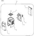
- FIG. 1 is a schematic diagram of a conventional power conversion device 8.
- FIG. 1 is an exploded view of each component when the power conversion device 8 is installed in a normal use state.
- the power conversion device 8 includes a semiconductor 4 that converts input DC power into AC power and a main circuit board 3 that drives the semiconductor 4.
- the main circuit board 3 and the semiconductor 4 are attached to the main body case 2 and are Covered.
- a surface cover 1 is attached to an opening located on the opposite side of the surface of the main body case 2 to which the main circuit board 3 and the semiconductor 4 are connected, and an upper surface wall 7 facing the installation surface of the main body case 2 is attached to the upper surface wall 7.
- a plurality of openings 9 are formed so that gas can flow in and out.
- a cooling fin 6 is attached adjacent to the main circuit board 3 and the semiconductor 4 to cool the heat generated in the main circuit board 3 and the semiconductor 4.
- FIG. 2 is an example of a configuration diagram of the power conversion device 8 of the present embodiment.
- the power converter 8 of this embodiment has a two-layer structure of the upper wall 7 having the opening of the main body case 2 of the conventional power converter 8 of FIG.
- the upper surface wall having a plurality of openings of the main body case 2 has a two-layer structure. Even if dust enters from the slit 10, which is a part, the structure can be prevented by the second non-opening portion that is staggered and does not enter the inside of the main body case 2.
- FIG. 3 is a detailed view of the top wall of the main body case of the power conversion device according to the first embodiment of the present invention.
- the upper surface wall having the opening of the main body case 2 has a two-layer structure, and the first and second layer openings of the upper surface wall 7 as shown in FIG.
- the shape is the same, and the shape is a pattern in which linear openings (slits 10) are arranged in parallel at intervals. Furthermore, the pattern of the opening and non-opening in the first layer and the pattern of the opening and non-opening in the second layer are alternated.
- the second layer non-opening is located below the first layer opening, and the second layer opening is located below the first layer non-opening.
- the main body case 2 can be structured so as not to enter the inside, and the safety in operation of the apparatus can be improved.
- an opening shape pattern in which straight slit-shaped openings are arranged in parallel has been described.
- the present invention is not limited to this shape pattern, and the second non-opening portion is located below the first opening portion. What is necessary is just to have the upper surface wall arrange
- FIG. 4 is a comparison diagram of air convection and dust contamination in the two-layer structure of the upper surface wall of the main body case of the power converter according to the first embodiment of the present invention and the conventional structure of the upper surface wall.
- the upper wall In the structure of the conventional upper wall on the left side, the upper wall is a single layer, and the substrate can be seen from the opening slit of the upper wall when viewed in the inner direction from directly above. Therefore, air convection tends to flow out of the main body case. Similarly, when there is a fallen object such as dust, the dust easily enters the inside of the main body case from the opening slit. For this reason, there was a problem in safety in terms of operating the apparatus.
- the upper surface wall of this embodiment on the right side has two layers, and the openings in the first layer and the second layer are alternately arranged. I can't see the board. Therefore, when there is a fallen object such as dust, even if it passes through the opening slit of the first layer, it prevents intrusion of dust etc. into the inside by the non-opening portion of the opening slit of the upper surface wall cover of the second layer. Is possible.
- FIG. 5 is a result of comparing the cooling performance of the power converter of Example 1 of the present invention and the conventional power converter of FIG.
- the structure of the opening of the upper surface wall of the main body case 2 of the conventional power converter 8 and the upper surface wall of the main body case 2 of this embodiment have a two-layer structure. Even when compared with the power converter 8, it was found that the wind speed flowing in or out did not change.
- FIG. 6 is an example of a configuration diagram of the power conversion device 8 according to the second embodiment of the present invention.
- the present embodiment is an example in which the top wall having a two-layer structure is detachable from the structure described in the first embodiment.
- the main body case 2 of the power conversion device 8 has a structure in which an upper surface wall is detachable and has a structure in which the upper surface wall can be removed.
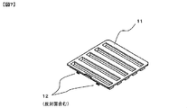
- FIG. 7 is a detailed view of the top wall cover 11 of this embodiment.
- the top wall cover 11 has the same structure as the two-layer structure of the top wall 7 of the first embodiment, and the dust that could not be prevented by the opening slit 10 in the first layer of the top wall cover 11 is two layers. It is prevented by the opening slit 10 of the eye. Therefore, it can suppress that dust etc. mix into the inside of an apparatus, and can improve the safety
- the top wall cover 11 can be attached to and detached from the main body case 2 by four claws 12 provided on the top wall cover 11.
- FIG. 7 only two pawls 12 are illustrated. However, two pawls 12 are further provided on the opposite surface on which the two pawls 12 are provided.
- the upper surface wall having the opening of the main body case has a two-layer structure, so that dust and the like can be prevented from being mixed into the apparatus, and the safety of the apparatus can be improved.
- the detachable top wall cover 11 is removed after the power conversion device 8 is turned off, and the top wall cover 11 is washed as it is. Therefore, it is possible to reduce the risk of dust entering the inside.
- FIG. 8 is an example of a configuration diagram of the power conversion device 8 according to the third embodiment of the present invention.
- Example 1 and Example 2 an example in which the semiconductor non-contact portion of the semiconductor installation surface of the cooling fin is covered with a heat insulating member 5 having heat insulating properties is shown.
- the heat of the semiconductor 4 is conducted to the cooling fin 6 in the conventional power converter 8 shown in FIG.
- the cooling fins are heated by the heat, and the heat is transmitted to the outside air and the main circuit board 3. This causes a problem that the operability and safety of the apparatus are lowered.
- the present invention is not limited to the above-described embodiments, and the opening of the main body case 2 having a two-layer structure is disposed on the side surface and the bottom surface, and the removable top wall cover 11 is disposed on the side surface of the main body case 2. Many modifications are included, such as disposing on various surfaces such as the bottom surface.
Landscapes
- Engineering & Computer Science (AREA)
- Microelectronics & Electronic Packaging (AREA)
- Power Engineering (AREA)
- Physics & Mathematics (AREA)
- Thermal Sciences (AREA)
- Inverter Devices (AREA)
- Cooling Or The Like Of Electrical Apparatus (AREA)
- Rectifiers (AREA)
Abstract
La présente invention a trait à un convertisseur de secteur qui est caractérisé en ce qu'il est doté d'un semi-conducteur, d'une carte de circuit primaire qui est pourvue d'un circuit permettant de commander le semi-conducteur, d'un boîtier permettant de loger la carte de circuit primaire et d'une ailette de refroidissement permettant de dissiper la chaleur de la carte de circuit primaire ; lequel boîtier est constitué d'une structure à deux couches dont la paroi de surface supérieure à l'opposé d'une surface sur laquelle le boîtier est monté est pourvue d'une pluralité d'ouvertures.
Priority Applications (1)
| Application Number | Priority Date | Filing Date | Title |
|---|---|---|---|
| CN201290001146.2U CN204090404U (zh) | 2012-02-15 | 2012-12-21 | 电力转换装置 |
Applications Claiming Priority (2)
| Application Number | Priority Date | Filing Date | Title |
|---|---|---|---|
| JP2012030112A JP2013168457A (ja) | 2012-02-15 | 2012-02-15 | 電力変換装置 |
| JP2012-030112 | 2012-02-15 |
Publications (1)
| Publication Number | Publication Date |
|---|---|
| WO2013121678A1 true WO2013121678A1 (fr) | 2013-08-22 |
Family
ID=48983820
Family Applications (1)
| Application Number | Title | Priority Date | Filing Date |
|---|---|---|---|
| PCT/JP2012/083189 Ceased WO2013121678A1 (fr) | 2012-02-15 | 2012-12-21 | Convertisseur de secteur |
Country Status (3)
| Country | Link |
|---|---|
| JP (1) | JP2013168457A (fr) |
| CN (1) | CN204090404U (fr) |
| WO (1) | WO2013121678A1 (fr) |
Citations (7)
| Publication number | Priority date | Publication date | Assignee | Title |
|---|---|---|---|---|
| JPS6170972U (fr) * | 1984-10-15 | 1986-05-15 | ||
| JPH0320489U (fr) * | 1989-03-16 | 1991-02-28 | ||
| JPH0353893U (fr) * | 1989-09-29 | 1991-05-24 | ||
| JPH0464881U (fr) * | 1990-10-12 | 1992-06-04 | ||
| JPH06120677A (ja) * | 1992-10-05 | 1994-04-28 | Meisei Electric Co Ltd | 筐体の通気構造 |
| WO2006030606A1 (fr) * | 2004-09-17 | 2006-03-23 | Kabushiki Kaisha Yaskawa Denki | Dispositif de commande de moteur et procédé d’assemblage de dispositif de commande de moteur |
| JP2007165423A (ja) * | 2005-12-12 | 2007-06-28 | Yaskawa Electric Corp | 電子機器装置 |
Family Cites Families (1)
| Publication number | Priority date | Publication date | Assignee | Title |
|---|---|---|---|---|
| JP2861506B2 (ja) * | 1991-08-05 | 1999-02-24 | 富士通株式会社 | 電子機器のモールド成形ケース |
-
2012
- 2012-02-15 JP JP2012030112A patent/JP2013168457A/ja active Pending
- 2012-12-21 CN CN201290001146.2U patent/CN204090404U/zh not_active Expired - Lifetime
- 2012-12-21 WO PCT/JP2012/083189 patent/WO2013121678A1/fr not_active Ceased
Patent Citations (7)
| Publication number | Priority date | Publication date | Assignee | Title |
|---|---|---|---|---|
| JPS6170972U (fr) * | 1984-10-15 | 1986-05-15 | ||
| JPH0320489U (fr) * | 1989-03-16 | 1991-02-28 | ||
| JPH0353893U (fr) * | 1989-09-29 | 1991-05-24 | ||
| JPH0464881U (fr) * | 1990-10-12 | 1992-06-04 | ||
| JPH06120677A (ja) * | 1992-10-05 | 1994-04-28 | Meisei Electric Co Ltd | 筐体の通気構造 |
| WO2006030606A1 (fr) * | 2004-09-17 | 2006-03-23 | Kabushiki Kaisha Yaskawa Denki | Dispositif de commande de moteur et procédé d’assemblage de dispositif de commande de moteur |
| JP2007165423A (ja) * | 2005-12-12 | 2007-06-28 | Yaskawa Electric Corp | 電子機器装置 |
Also Published As
| Publication number | Publication date |
|---|---|
| JP2013168457A (ja) | 2013-08-29 |
| CN204090404U (zh) | 2015-01-07 |
Similar Documents
| Publication | Publication Date | Title |
|---|---|---|
| CN205249640U (zh) | 工业用不断电系统机箱结构 | |
| KR100997012B1 (ko) | 전력 변환 장치 | |
| TWI426860B (zh) | 熱交換裝置及應用熱交換裝置的密閉式電器設備 | |
| US8755183B2 (en) | Car electric equipment case module | |
| CN103415431B (zh) | 车辆用控制装置 | |
| JP5554651B2 (ja) | 電力変換装置 | |
| JP5965779B2 (ja) | 電力変換装置 | |
| JP6433631B2 (ja) | 電力変換装置 | |
| JP6094416B2 (ja) | 電力変換装置 | |
| CN105408183A (zh) | 用于车辆的电力变换装置以及铁路车辆 | |
| US20130092431A1 (en) | Enclosure | |
| JP2000286580A (ja) | 電子装置の冷却装置 | |
| JP5380262B2 (ja) | 電力変換装置及びエレベータの制御装置 | |
| WO2013121678A1 (fr) | Convertisseur de secteur | |
| US11540427B2 (en) | Converter having a separate interior | |
| JP4725338B2 (ja) | モータ駆動装置の冷却構造 | |
| JP2004349548A (ja) | ヒートシンクとこれを備えた電気制御装置 | |
| JPH04338074A (ja) | エレベータ制御盤 | |
| JP2017112190A (ja) | 冷却装置および電力変換装置 | |
| CN211128745U (zh) | 电机控制器 | |
| JP7662951B2 (ja) | 電装品箱および換気装置 | |
| KR20180073263A (ko) | 이더넷 스위치의 방열구조 | |
| KR101287664B1 (ko) | 히트 싱크 모듈 | |
| CN116715111B (zh) | 电梯控制柜 | |
| KR20160043689A (ko) | 전자기기의 캐비닛 |
Legal Events
| Date | Code | Title | Description |
|---|---|---|---|
| WWE | Wipo information: entry into national phase |
Ref document number: 201290001146.2 Country of ref document: CN |
|
| 121 | Ep: the epo has been informed by wipo that ep was designated in this application |
Ref document number: 12868497 Country of ref document: EP Kind code of ref document: A1 |
|
| NENP | Non-entry into the national phase |
Ref country code: DE |
|
| 122 | Ep: pct application non-entry in european phase |
Ref document number: 12868497 Country of ref document: EP Kind code of ref document: A1 |