WO2013129253A1 - Dispositif semi-conducteur, son procédé de fabrication et câble de connexion - Google Patents
Dispositif semi-conducteur, son procédé de fabrication et câble de connexion Download PDFInfo
- Publication number
- WO2013129253A1 WO2013129253A1 PCT/JP2013/054524 JP2013054524W WO2013129253A1 WO 2013129253 A1 WO2013129253 A1 WO 2013129253A1 JP 2013054524 W JP2013054524 W JP 2013054524W WO 2013129253 A1 WO2013129253 A1 WO 2013129253A1
- Authority
- WO
- WIPO (PCT)
- Prior art keywords
- wire
- electrode
- metal
- power semiconductor
- coating layer
- Prior art date
- Legal status (The legal status is an assumption and is not a legal conclusion. Google has not performed a legal analysis and makes no representation as to the accuracy of the status listed.)
- Ceased
Links
Images

Classifications
-
- H—ELECTRICITY
- H10—SEMICONDUCTOR DEVICES; ELECTRIC SOLID-STATE DEVICES NOT OTHERWISE PROVIDED FOR
- H10W—GENERIC PACKAGES, INTERCONNECTIONS, CONNECTORS OR OTHER CONSTRUCTIONAL DETAILS OF DEVICES COVERED BY CLASS H10
- H10W72/00—Interconnections or connectors in packages
- H10W72/90—Bond pads, in general
-
- H—ELECTRICITY
- H10—SEMICONDUCTOR DEVICES; ELECTRIC SOLID-STATE DEVICES NOT OTHERWISE PROVIDED FOR
- H10W—GENERIC PACKAGES, INTERCONNECTIONS, CONNECTORS OR OTHER CONSTRUCTIONAL DETAILS OF DEVICES COVERED BY CLASS H10
- H10W72/00—Interconnections or connectors in packages
- H10W72/01—Manufacture or treatment
- H10W72/015—Manufacture or treatment of bond wires
-
- H—ELECTRICITY
- H10—SEMICONDUCTOR DEVICES; ELECTRIC SOLID-STATE DEVICES NOT OTHERWISE PROVIDED FOR
- H10W—GENERIC PACKAGES, INTERCONNECTIONS, CONNECTORS OR OTHER CONSTRUCTIONAL DETAILS OF DEVICES COVERED BY CLASS H10
- H10W72/00—Interconnections or connectors in packages
- H10W72/01—Manufacture or treatment
- H10W72/019—Manufacture or treatment of bond pads
-
- H—ELECTRICITY
- H10—SEMICONDUCTOR DEVICES; ELECTRIC SOLID-STATE DEVICES NOT OTHERWISE PROVIDED FOR
- H10W—GENERIC PACKAGES, INTERCONNECTIONS, CONNECTORS OR OTHER CONSTRUCTIONAL DETAILS OF DEVICES COVERED BY CLASS H10
- H10W72/00—Interconnections or connectors in packages
- H10W72/071—Connecting or disconnecting
- H10W72/075—Connecting or disconnecting of bond wires
-
- H—ELECTRICITY
- H10—SEMICONDUCTOR DEVICES; ELECTRIC SOLID-STATE DEVICES NOT OTHERWISE PROVIDED FOR
- H10W—GENERIC PACKAGES, INTERCONNECTIONS, CONNECTORS OR OTHER CONSTRUCTIONAL DETAILS OF DEVICES COVERED BY CLASS H10
- H10W72/00—Interconnections or connectors in packages
- H10W72/50—Bond wires
-
- H—ELECTRICITY
- H10—SEMICONDUCTOR DEVICES; ELECTRIC SOLID-STATE DEVICES NOT OTHERWISE PROVIDED FOR
- H10W—GENERIC PACKAGES, INTERCONNECTIONS, CONNECTORS OR OTHER CONSTRUCTIONAL DETAILS OF DEVICES COVERED BY CLASS H10
- H10W72/00—Interconnections or connectors in packages
- H10W72/01—Manufacture or treatment
- H10W72/015—Manufacture or treatment of bond wires
- H10W72/01515—Forming coatings
-
- H—ELECTRICITY
- H10—SEMICONDUCTOR DEVICES; ELECTRIC SOLID-STATE DEVICES NOT OTHERWISE PROVIDED FOR
- H10W—GENERIC PACKAGES, INTERCONNECTIONS, CONNECTORS OR OTHER CONSTRUCTIONAL DETAILS OF DEVICES COVERED BY CLASS H10
- H10W72/00—Interconnections or connectors in packages
- H10W72/01—Manufacture or treatment
- H10W72/015—Manufacture or treatment of bond wires
- H10W72/01551—Changing the shapes of bond wires
-
- H—ELECTRICITY
- H10—SEMICONDUCTOR DEVICES; ELECTRIC SOLID-STATE DEVICES NOT OTHERWISE PROVIDED FOR
- H10W—GENERIC PACKAGES, INTERCONNECTIONS, CONNECTORS OR OTHER CONSTRUCTIONAL DETAILS OF DEVICES COVERED BY CLASS H10
- H10W72/00—Interconnections or connectors in packages
- H10W72/01—Manufacture or treatment
- H10W72/015—Manufacture or treatment of bond wires
- H10W72/01565—Thermally treating
-
- H—ELECTRICITY
- H10—SEMICONDUCTOR DEVICES; ELECTRIC SOLID-STATE DEVICES NOT OTHERWISE PROVIDED FOR
- H10W—GENERIC PACKAGES, INTERCONNECTIONS, CONNECTORS OR OTHER CONSTRUCTIONAL DETAILS OF DEVICES COVERED BY CLASS H10
- H10W72/00—Interconnections or connectors in packages
- H10W72/01—Manufacture or treatment
- H10W72/019—Manufacture or treatment of bond pads
- H10W72/01931—Manufacture or treatment of bond pads using blanket deposition
- H10W72/01933—Manufacture or treatment of bond pads using blanket deposition in liquid form, e.g. spin coating, spray coating or immersion coating
- H10W72/01935—Manufacture or treatment of bond pads using blanket deposition in liquid form, e.g. spin coating, spray coating or immersion coating by plating, e.g. electroless plating or electroplating
-
- H—ELECTRICITY
- H10—SEMICONDUCTOR DEVICES; ELECTRIC SOLID-STATE DEVICES NOT OTHERWISE PROVIDED FOR
- H10W—GENERIC PACKAGES, INTERCONNECTIONS, CONNECTORS OR OTHER CONSTRUCTIONAL DETAILS OF DEVICES COVERED BY CLASS H10
- H10W72/00—Interconnections or connectors in packages
- H10W72/01—Manufacture or treatment
- H10W72/019—Manufacture or treatment of bond pads
- H10W72/01931—Manufacture or treatment of bond pads using blanket deposition
- H10W72/01938—Manufacture or treatment of bond pads using blanket deposition in gaseous form, e.g. by CVD or PVD
-
- H—ELECTRICITY
- H10—SEMICONDUCTOR DEVICES; ELECTRIC SOLID-STATE DEVICES NOT OTHERWISE PROVIDED FOR
- H10W—GENERIC PACKAGES, INTERCONNECTIONS, CONNECTORS OR OTHER CONSTRUCTIONAL DETAILS OF DEVICES COVERED BY CLASS H10
- H10W72/00—Interconnections or connectors in packages
- H10W72/071—Connecting or disconnecting
- H10W72/0711—Apparatus therefor
- H10W72/07141—Means for applying energy, e.g. ovens or lasers
-
- H—ELECTRICITY
- H10—SEMICONDUCTOR DEVICES; ELECTRIC SOLID-STATE DEVICES NOT OTHERWISE PROVIDED FOR
- H10W—GENERIC PACKAGES, INTERCONNECTIONS, CONNECTORS OR OTHER CONSTRUCTIONAL DETAILS OF DEVICES COVERED BY CLASS H10
- H10W72/00—Interconnections or connectors in packages
- H10W72/071—Connecting or disconnecting
- H10W72/075—Connecting or disconnecting of bond wires
- H10W72/07531—Techniques
- H10W72/07532—Compression bonding, e.g. thermocompression bonding
- H10W72/07533—Ultrasonic bonding, e.g. thermosonic bonding
-
- H—ELECTRICITY
- H10—SEMICONDUCTOR DEVICES; ELECTRIC SOLID-STATE DEVICES NOT OTHERWISE PROVIDED FOR
- H10W—GENERIC PACKAGES, INTERCONNECTIONS, CONNECTORS OR OTHER CONSTRUCTIONAL DETAILS OF DEVICES COVERED BY CLASS H10
- H10W72/00—Interconnections or connectors in packages
- H10W72/50—Bond wires
- H10W72/521—Structures or relative sizes of bond wires
- H10W72/522—Multilayered bond wires, e.g. having a coating concentric around a core
- H10W72/523—Multilayered bond wires, e.g. having a coating concentric around a core characterised by the structures of the outermost layers, e.g. multilayered coatings
-
- H—ELECTRICITY
- H10—SEMICONDUCTOR DEVICES; ELECTRIC SOLID-STATE DEVICES NOT OTHERWISE PROVIDED FOR
- H10W—GENERIC PACKAGES, INTERCONNECTIONS, CONNECTORS OR OTHER CONSTRUCTIONAL DETAILS OF DEVICES COVERED BY CLASS H10
- H10W72/00—Interconnections or connectors in packages
- H10W72/50—Bond wires
- H10W72/531—Shapes of wire connectors
- H10W72/536—Shapes of wire connectors the connected ends being ball-shaped
-
- H—ELECTRICITY
- H10—SEMICONDUCTOR DEVICES; ELECTRIC SOLID-STATE DEVICES NOT OTHERWISE PROVIDED FOR
- H10W—GENERIC PACKAGES, INTERCONNECTIONS, CONNECTORS OR OTHER CONSTRUCTIONAL DETAILS OF DEVICES COVERED BY CLASS H10
- H10W72/00—Interconnections or connectors in packages
- H10W72/50—Bond wires
- H10W72/531—Shapes of wire connectors
- H10W72/5363—Shapes of wire connectors the connected ends being wedge-shaped
-
- H—ELECTRICITY
- H10—SEMICONDUCTOR DEVICES; ELECTRIC SOLID-STATE DEVICES NOT OTHERWISE PROVIDED FOR
- H10W—GENERIC PACKAGES, INTERCONNECTIONS, CONNECTORS OR OTHER CONSTRUCTIONAL DETAILS OF DEVICES COVERED BY CLASS H10
- H10W72/00—Interconnections or connectors in packages
- H10W72/50—Bond wires
- H10W72/551—Materials of bond wires
- H10W72/552—Materials of bond wires comprising metals or metalloids, e.g. silver
- H10W72/5522—Materials of bond wires comprising metals or metalloids, e.g. silver comprising gold [Au]
-
- H—ELECTRICITY
- H10—SEMICONDUCTOR DEVICES; ELECTRIC SOLID-STATE DEVICES NOT OTHERWISE PROVIDED FOR
- H10W—GENERIC PACKAGES, INTERCONNECTIONS, CONNECTORS OR OTHER CONSTRUCTIONAL DETAILS OF DEVICES COVERED BY CLASS H10
- H10W72/00—Interconnections or connectors in packages
- H10W72/50—Bond wires
- H10W72/551—Materials of bond wires
- H10W72/552—Materials of bond wires comprising metals or metalloids, e.g. silver
- H10W72/5524—Materials of bond wires comprising metals or metalloids, e.g. silver comprising aluminium [Al]
-
- H—ELECTRICITY
- H10—SEMICONDUCTOR DEVICES; ELECTRIC SOLID-STATE DEVICES NOT OTHERWISE PROVIDED FOR
- H10W—GENERIC PACKAGES, INTERCONNECTIONS, CONNECTORS OR OTHER CONSTRUCTIONAL DETAILS OF DEVICES COVERED BY CLASS H10
- H10W72/00—Interconnections or connectors in packages
- H10W72/50—Bond wires
- H10W72/551—Materials of bond wires
- H10W72/552—Materials of bond wires comprising metals or metalloids, e.g. silver
- H10W72/5525—Materials of bond wires comprising metals or metalloids, e.g. silver comprising copper [Cu]
-
- H—ELECTRICITY
- H10—SEMICONDUCTOR DEVICES; ELECTRIC SOLID-STATE DEVICES NOT OTHERWISE PROVIDED FOR
- H10W—GENERIC PACKAGES, INTERCONNECTIONS, CONNECTORS OR OTHER CONSTRUCTIONAL DETAILS OF DEVICES COVERED BY CLASS H10
- H10W72/00—Interconnections or connectors in packages
- H10W72/50—Bond wires
- H10W72/551—Materials of bond wires
- H10W72/553—Materials of bond wires not comprising solid metals or solid metalloids, e.g. polymers, ceramics or liquids
-
- H—ELECTRICITY
- H10—SEMICONDUCTOR DEVICES; ELECTRIC SOLID-STATE DEVICES NOT OTHERWISE PROVIDED FOR
- H10W—GENERIC PACKAGES, INTERCONNECTIONS, CONNECTORS OR OTHER CONSTRUCTIONAL DETAILS OF DEVICES COVERED BY CLASS H10
- H10W72/00—Interconnections or connectors in packages
- H10W72/50—Bond wires
- H10W72/551—Materials of bond wires
- H10W72/555—Materials of bond wires of outermost layers of multilayered bond wires, e.g. material of a coating
-
- H—ELECTRICITY
- H10—SEMICONDUCTOR DEVICES; ELECTRIC SOLID-STATE DEVICES NOT OTHERWISE PROVIDED FOR
- H10W—GENERIC PACKAGES, INTERCONNECTIONS, CONNECTORS OR OTHER CONSTRUCTIONAL DETAILS OF DEVICES COVERED BY CLASS H10
- H10W72/00—Interconnections or connectors in packages
- H10W72/50—Bond wires
- H10W72/59—Bond pads specially adapted therefor
-
- H—ELECTRICITY
- H10—SEMICONDUCTOR DEVICES; ELECTRIC SOLID-STATE DEVICES NOT OTHERWISE PROVIDED FOR
- H10W—GENERIC PACKAGES, INTERCONNECTIONS, CONNECTORS OR OTHER CONSTRUCTIONAL DETAILS OF DEVICES COVERED BY CLASS H10
- H10W72/00—Interconnections or connectors in packages
- H10W72/851—Dispositions of multiple connectors or interconnections
- H10W72/874—On different surfaces
- H10W72/884—Die-attach connectors and bond wires
-
- H—ELECTRICITY
- H10—SEMICONDUCTOR DEVICES; ELECTRIC SOLID-STATE DEVICES NOT OTHERWISE PROVIDED FOR
- H10W—GENERIC PACKAGES, INTERCONNECTIONS, CONNECTORS OR OTHER CONSTRUCTIONAL DETAILS OF DEVICES COVERED BY CLASS H10
- H10W72/00—Interconnections or connectors in packages
- H10W72/90—Bond pads, in general
- H10W72/921—Structures or relative sizes of bond pads
- H10W72/923—Bond pads having multiple stacked layers
-
- H—ELECTRICITY
- H10—SEMICONDUCTOR DEVICES; ELECTRIC SOLID-STATE DEVICES NOT OTHERWISE PROVIDED FOR
- H10W—GENERIC PACKAGES, INTERCONNECTIONS, CONNECTORS OR OTHER CONSTRUCTIONAL DETAILS OF DEVICES COVERED BY CLASS H10
- H10W72/00—Interconnections or connectors in packages
- H10W72/90—Bond pads, in general
- H10W72/951—Materials of bond pads
- H10W72/952—Materials of bond pads comprising metals or metalloids, e.g. PbSn, Ag or Cu
-
- H—ELECTRICITY
- H10—SEMICONDUCTOR DEVICES; ELECTRIC SOLID-STATE DEVICES NOT OTHERWISE PROVIDED FOR
- H10W—GENERIC PACKAGES, INTERCONNECTIONS, CONNECTORS OR OTHER CONSTRUCTIONAL DETAILS OF DEVICES COVERED BY CLASS H10
- H10W90/00—Package configurations
- H10W90/701—Package configurations characterised by the relative positions of pads or connectors relative to package parts
- H10W90/731—Package configurations characterised by the relative positions of pads or connectors relative to package parts of die-attach connectors
- H10W90/736—Package configurations characterised by the relative positions of pads or connectors relative to package parts of die-attach connectors between a chip and a stacked lead frame, conducting package substrate or heat sink
-
- H—ELECTRICITY
- H10—SEMICONDUCTOR DEVICES; ELECTRIC SOLID-STATE DEVICES NOT OTHERWISE PROVIDED FOR
- H10W—GENERIC PACKAGES, INTERCONNECTIONS, CONNECTORS OR OTHER CONSTRUCTIONAL DETAILS OF DEVICES COVERED BY CLASS H10
- H10W90/00—Package configurations
- H10W90/701—Package configurations characterised by the relative positions of pads or connectors relative to package parts
- H10W90/751—Package configurations characterised by the relative positions of pads or connectors relative to package parts of bond wires
- H10W90/753—Package configurations characterised by the relative positions of pads or connectors relative to package parts of bond wires between laterally-adjacent chips
-
- H—ELECTRICITY
- H10—SEMICONDUCTOR DEVICES; ELECTRIC SOLID-STATE DEVICES NOT OTHERWISE PROVIDED FOR
- H10W—GENERIC PACKAGES, INTERCONNECTIONS, CONNECTORS OR OTHER CONSTRUCTIONAL DETAILS OF DEVICES COVERED BY CLASS H10
- H10W90/00—Package configurations
- H10W90/701—Package configurations characterised by the relative positions of pads or connectors relative to package parts
- H10W90/751—Package configurations characterised by the relative positions of pads or connectors relative to package parts of bond wires
- H10W90/754—Package configurations characterised by the relative positions of pads or connectors relative to package parts of bond wires between a chip and a stacked insulating package substrate, interposer or RDL
-
- H—ELECTRICITY
- H10—SEMICONDUCTOR DEVICES; ELECTRIC SOLID-STATE DEVICES NOT OTHERWISE PROVIDED FOR
- H10W—GENERIC PACKAGES, INTERCONNECTIONS, CONNECTORS OR OTHER CONSTRUCTIONAL DETAILS OF DEVICES COVERED BY CLASS H10
- H10W90/00—Package configurations
- H10W90/701—Package configurations characterised by the relative positions of pads or connectors relative to package parts
- H10W90/751—Package configurations characterised by the relative positions of pads or connectors relative to package parts of bond wires
- H10W90/756—Package configurations characterised by the relative positions of pads or connectors relative to package parts of bond wires between a chip and a stacked lead frame, conducting package substrate or heat sink
Definitions
- the present invention relates to a power semiconductor device, a manufacturing method thereof, and a bonding wire used in the power semiconductor device.
- This application claims priority based on Japanese Patent Application No. 2012-040116 for which it applied to Japan on February 27, 2012, and uses the content here.
- a power semiconductor means a semiconductor used for control and supply of electric energy, such as converting alternating current to direct current or lowering voltage. Compared to LSI or the like, the current flowing in the semiconductor circuit is a large current.
- Power semiconductor devices are widely used for various motor controls, power converters, and uninterruptible power supplies.
- a power semiconductor device power semiconductor module
- power semiconductor switching elements such as IGBT (Insulated Gate Bipolar Transistor), GTO, and power transistor are packaged in an insulating container.
- IGBT Insulated Gate Bipolar Transistor
- GTO Insulated Gate Bipolar Transistor
- power transistor are packaged in an insulating container.
- IGBT Insulated Gate Bipolar Transistor
- GTO Insulated Gate Bipolar Transistor
- power transistor are packaged in an insulating container.
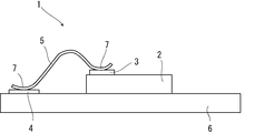
- FIG. 1 shows a schematic partial cross-sectional view of the power semiconductor device 1.
- a metal electrode is provided on the power semiconductor element 2, and one end of a metal wire 5 is connected to the metal electrode, and a lead frame of the power semiconductor device, an electrode on the substrate 6, or another mounted power semiconductor element
- a circuit is configured by connecting the other end of the metal wire to the metal electrode.
- the metal electrode on the target power semiconductor element 2 is referred to as “element electrode 3”
- connection electrode 4 the metal electrode for connecting to the element electrode 3
- a large-diameter Al wire having a diameter of several hundred ⁇ m is usually used as the metal wire for connecting electrodes (Patent Document 1).
- a Cu wire is used as a metal wire in a part of the LSI, but it is not used as a large-diameter wire of a power semiconductor device. This is because the Cu wire has high hardness and work hardening index, and in particular, has a high probability of damaging the device electrode when connected by ultrasonic waves with a thick wire diameter.
- Gold wires are frequently used for ball bonding of LSIs, but material costs are particularly high for thick wire diameters used in power semiconductor devices, so that they have hardly been put to practical use.
- Patent Document 2 discloses a bonding wire in which a core material made only of Ag or an Ag alloy is covered with a skin material made only of Au.
- Patent Document 3 discloses a bonding wire having a coating layer containing Pd, Pt, and Ni on a core material containing Ag. However, both are intended for thin diameters of 25 ⁇ m or 40 ⁇ m or less. Further, as described in Patent Document 2, when an Ag wire is bonded to an Al electrode, the formation of an Al 2 Ag intermetallic compound is remarkable, and this intermetallic compound is very brittle. In particular, the Ag wire cannot be used for the power semiconductor device.
- Patent Document 4 discloses an example in which Ag is used as a conductor for joining an electrode and a pad as a power semiconductor module, but the conductor, the pad and the electrode are joined by soldering, and ball bonding or wedge bonding is performed. Not intended.
- a gold-based surface metal layer is provided on an aluminum-based or copper-based bonding pad on a semiconductor chip, which is a part of a semiconductor integrated circuit device, via a barrier metal film.
- a metal-based or copper-based bonding wire bond or a bonding ball for connection to a wire is disclosed. This is to prevent connection failure such as Kirkendall void due to the interaction between aluminum and gold. It is intended only for gold wires or copper wires, and is not intended for power semiconductor devices using thick wires.
- power semiconductor devices using a power semiconductor element having a SiC substrate that has been attracting attention in recent years can operate at a high temperature of 250 ° C. or higher because the band gap of the SiC crystal is much larger than that of the Si crystal.
- Power semiconductor devices that are premised on operation at high temperatures are being studied. In such a power semiconductor device that is premised on operation at a high temperature, the heat resistance of the device becomes more and more important.
- Conventionally used Al wire has a relatively low melting point of around 660 ° C., so recrystallization occurs when used at a high temperature, and cracks and void defects are likely to occur inside the wire and at the interface of the joint. is there.
- JP 2002-314038 A Japanese Patent Laid-Open No. 2-79439 JP 2004-14884 A Japanese Patent Laid-Open No. 9-36186 JP 2010-157683 A
- Al wire as a metal wire for connection in power semiconductor devices has the advantage that it has a low hardness at room temperature and can be bonded to the Al electrode on the element side relatively easily by ultrasonic vibration. is there.
- Al has a low melting point of around 660 ° C., so that the heat resistance at high temperature is not sufficient, and Al has a specific resistance. Is 2.7 ⁇ ⁇ cm, which is the highest among the good conductors, and the heat generation of the wire when a large current is passed through the Al wire cannot be ignored.
- the thermal stress causes a stress migration of Al and causes defects.
- resistance increases further with increasing temperature, so defects especially during aluminum grain growth and recrystallization are not only problematic when used at high temperatures. There is also concern about being connected.
- the present invention can increase the current capacity of a power semiconductor device and can be used without any problem even when thermal stress occurs when used in a high temperature environment, and can reduce the heat generation of the wire itself, for example, even in a high temperature environment of 200 ° C. or higher. It is an object of the present invention to provide a power semiconductor device capable of ensuring the reliability of the joint, a manufacturing method thereof, and a bonding wire used in the power semiconductor device.
- the specific resistance of Ag is 1.6 ⁇ ⁇ cm, which is lower than 2.7 ⁇ ⁇ cm of Al. Heat generation of the wire itself can be reduced.
- Ag has a melting point of 962 ° C., which is much higher than the melting point of Al, 660 ° C., and can improve heat resistance at high temperatures. Since Ag has a higher melting point than Al, defects due to stress migration are less likely to occur.
- it compared with Cu, it has high deformability and can absorb stress, so it has excellent resistance to breakage such as cracks caused by thermal stress.
- an Ag wire has a low hardness at normal temperature and a low work hardening, so that the possibility of element electrode damage during bonding by applying ultrasonic waves during wire bonding is low.
- the inventors used any one kind of metal of Ni, Cr, Cu, Pd, V, Ti, Pt, Zn, Ag, Au, W, and Al having a thickness of 50 mm or more for the element electrode or these.
- Using one or more layers composed only of an alloy composed of only two or more types, electrodes having adjacent element electrodes and metal components of the layers different from each other, and wire bonding instead of ball bonding By using (wedge bonding), it has been found that the reliability of the electrode and the wire bonding portion can be secured even when Ag or an Ag alloy wire is used as the metal wire.
- a power semiconductor element a metal electrode (hereinafter referred to as “element electrode”) on the power semiconductor element, and a metal electrode (hereinafter referred to as “connection electrode”) for connection to the element electrode
- the metal wire is an Ag or Ag alloy wire having a diameter of more than 50 ⁇ m and 2 mm or less
- the element electrode is Ni, Cr, Cu, Pd, V, Ti, Pt, Zn, Ag, Au, W, Al metal (hereinafter referred to as “coating layer metal”), or only one type of metal or two or more types of the coating layer metal.
- Electrode covering layer One or more layers composed of an alloy only (hereinafter referred to as an “electrode covering layer”) have different metal components in the adjacent element electrode and electrode covering layer, and the element electrode is A
- the outermost layer of the electrode coating layer is Ag in the electrode, any one of the metals obtained by removing Ag from the coating layer metal below the outermost electrode coating layer, or two types of the coating layer metal
- a power semiconductor device comprising: one or more electrode coating layers composed of only an alloy composed of the above components so that the metal components of the adjacent element electrode and electrode coating layer are different.
- the power semiconductor device according to any one of (1) to (4), wherein the power semiconductor element is an element using a SiC semiconductor.
- the connection between the Ag or Ag alloy wire and the element electrode and the connection electrode is performed using ultrasonic waves, and the temperature of either the electrode or the wire at the time of connection is 60 ° C. or higher.
- the method for manufacturing a power semiconductor device according to the above (1) or (2).
- a coating layer on the surface of the wire is formed by coating by wet, dry, or nanoparticle metal deposition. Manufacturing method.
- Ag or Ag alloy bonding wire for semiconductor connection having a diameter of more than 50 ⁇ m and 2 mm or less, and having one or more of Pd, Au, Zn, Pt, Ni, Sn on the surface thereof, an alloy thereof or a metal thereof
- a bonding wire comprising a wire coating layer comprising an oxide or a nitride.
- a metal and Ag diffusion layer of the wire coating layer is provided between the wire coating layer and the wire base material, and the thickness of the diffusion layer is 50 mm or more and 10 ⁇ m or less (8) ) Or the bonding wire according to (9).
- the present invention includes a power semiconductor element, a metal electrode (element electrode) on the power semiconductor element, and a metal electrode (connection electrode) for connecting to the element electrode, and the element electrode and the connection electrode are both connected by a metal wire.
- the metal wire is an Ag or Ag alloy wire having a diameter of more than 50 ⁇ m and 2 mm or less
- the element electrode has a coating layer metal (Ni, Cr, Cu, Pd, V, Ti, having a thickness of 50 mm or more on the surface. , Pt, Zn, Ag, Au, W, Al), or one or more electrode coating layers that are layers composed of only one type of metal or an alloy composed of only two or more types of the coating layer metal.
- an Al electrode, a Cu electrode, a Ni electrode, or a Ti electrode can be used, and an Al electrode is preferably used.
- an Al electrode is used as the element electrode.
- an intermetallic compound such as Ag 2 Al is generated at the interface when a large Ag or Ag alloy wire having a diameter of more than 50 ⁇ m is joined to the Al electrode, and the metal Since the intermetallic compound is very brittle and voids are generated at the site where the intermetallic compound is produced, it is difficult to bond with good reliability.
- any one of coating layer metals Ni, Cr, Cu, Pd, V, Ti, Pt, Zn, Ag, Au, W, Al having a thickness of 50 mm or more is provided.
- an electrode having one or more electrode coating layers composed of only metal or an alloy composed of only two or more types of the coating layer metal so that the metal components of the adjacent element electrode and electrode coating layer are different Further, it has been found that by using wedge bonding for wire bonding, the reliability of the electrode and wire bonding portion can be ensured even when a large diameter Ag or Ag alloy wire having a diameter of more than 50 ⁇ m is used as the metal wire.
- adjacent element electrodes are formed when forming one or more electrode coating layers on the surface of the element electrode.
- the metal components of the metal or alloy constituting the electrode coating layer are different, and the electrode coating layers of Al, Cu, Ni and Ti are formed on the Al electrode, Cu electrode, Ni electrode and Ti electrode, respectively. Or an electrode covering layer composed of only the same kind of covering layer metal or its alloy is excluded.
- an electrode coating layer composed only of a coating layer metal or a coating layer metal alloy on the surface of the Al electrode
- these metals are different from the Al electrode and are bonded to Al and Ag.
- the formation of intermetallic compounds with many defects such as voids formed in the portion can be suppressed.
- these metals and Ag can form a diffusion layer at a relatively good joint by ultrasonic bonding.
- a noble metal such as Pd, Au, Ag, etc. to prevent oxidation.
- V, Ti, Cr, and Ni are effective in adhesion to the Al electrode, and also function effectively as a diffusion barrier between Ag and Al.
- Cu, Pd, Pt, and Zn are suitable for improving initial bondability with Ag. It is also effective to stack a plurality of layers of these metals in order to ensure initial bondability and long-term bond reliability.
- the thickness of the electrode coating layer is 50 mm or more, the above effect can be exhibited. This is because if it is less than 50 mm, defects are likely to occur in the electrode coating layer. Therefore, when laminating a plurality of electrode coating layers, the thickness of each electrode coating layer is 50 mm or more. More preferably, the thickness of the electrode coating layer is 100 mm or more. More preferably, it is 200 mm or more.
- the upper limit of the thickness of the electrode coating layer is preferably 5 ⁇ m. This is because if it exceeds 5 ⁇ m, the cost becomes high and the electric resistance value of the joint portion varies depending on the joining condition.
- an electrode coating layer composed only of Ag or Au is used as the coating layer metal constituting the outermost electrode coating layer on the Al electrode
- an electrode coating layer composed only of Ag or Au is directly provided on the Al electrode.
- Ni, Cr, Cu, Pd, V, Ti, Pt, Zn, Au which is an intermediate layer between the Al electrode and the electrode coating layer composed only of Ag or Au, excluding Ag from the coating layer metal.
- Metal component of the element electrode and the electrode coating layer adjacent to one or more of the electrode coating layer composed of only an alloy composed of only one kind of metal of W or Al or two or more kinds of metals of the coating layer metal Are preferably different from each other.
- the metal used for these intermediate layers has adhesiveness and diffusion barrier properties, it is possible to avoid the problem of voids formed due to the compounds generated by the reaction at the time of temperature rise.
- Cr is taken as an example.
- the coating layer has the effect of improving the adhesion with the surface of the Al electrode
- the Ni coating layer has the function of preventing diffusion and blocking the formation of Al and Ag compounds
- the outermost Ag coating layer is coated with Ni. It has a function of preventing surface oxidation of the layer.
- a combination of metals having adhesion and diffusion barrier properties such as / Cu / Ag and Al / Zn / Pd / Ni / Ag is preferable.
- the structure of the film used for these intermediate layers is not limited to the case where the outermost surface layer is Ag, but is used as an intermediate layer between the Al electrode and the outermost surface metal, thereby improving the reliability of bonding with the Ag wire. Effective to enhance.
- the use of Ag, Au, or Pd as the outermost surface layer of the electrode coating layer has the effect of preventing the oxidation of the underlying intermediate layer metal.
- the outermost layer is Ag
- an electrode coating layer composed only of a metal obtained by removing Ag from the coating layer metal or an alloy composed of only two or more types of coating layer metals is provided in the intermediate layer below it. By having it, formation of intermetallic compounds by the Ag layer and the Al electrode can be prevented.
- the electrode coating layer may be an Ag single layer.
- the use of a Cu electrode as a wire bonding electrode of a semiconductor element has not been studied in the past, but the use of Cu as an electrode of a semiconductor element for the purpose of using a wire mainly composed of Ag as a wedge wire. Is preferred.
- the Ag wire can remarkably reduce chip damage at the time of bonding as compared with the Cu wire, but the hardness is higher than that of the conventional Al wire. Therefore, by adopting a Cu electrode in place of a conventional Al electrode having a low hardness at the joint portion of the Ag wire, an effect of reducing the probability of chip damage appears.
- the electrode coating layer has a thickness of 3 ⁇ m or more, the effect can be further enhanced.
- a mutual diffusion layer of Cu and Ag is formed to have a thickness of 0.1 ⁇ m or more.
- the electrode covering layer has at least one metal layer of Au, Pd, Ni or an alloy layer thereof for the purpose of preventing oxidation. Yes, desirable.
- a metal different from the electrode material on the surface may be disposed below the electrode surface.
- a layer having an Al layer on the electrode surface and a metal different from Al, for example, Cu may be formed in the lower layer.
- the metal used for the internal wiring of the semiconductor element is Cu
- the element electrode is an Al electrode
- an Al layer is formed on the electrode surface, and the same Cu layer as the internal wiring of the semiconductor element is formed in the lower layer.
- a Cu layer may be provided on the electrode surface, and the same Al layer as the internal wiring of the semiconductor element may be formed in the lower layer.
- the Ag wire refers to a wire using Ag with an Ag content of 99% by mass or more.
- an Ag alloy wire means the wire using Ag alloy whose Ag content is 50 mass% or more.
- an Ag alloy added with Au, Pd, or both is particularly effective.
- Ag has a problem of being easily sulfided, and an alloy with Au is effective for suppressing this.
- an intermetallic compound such as Ag 2 Al is formed by bonding with Al, and an alloy of Ag and Pd is effective for this suppression.
- Au is desirably 1% by mass or more and 10% by mass or less, and Pd is desirably 0.1% by mass or more and 5% by mass or less.
- the Ag or Ag alloy wire targeted by the present invention is intended for those having a diameter of more than 50 ⁇ m and 2 mm or less. This is because the effect of the present invention is particularly remarkable when the wire diameter exceeds 50 ⁇ m. More preferably, the wire diameter is 150 ⁇ m or more. More preferably, the wire diameter is 200 ⁇ m or more. However, if the wire diameter exceeds 2 mm, the ultrasonic output for obtaining the necessary deformation at the time of joining becomes excessive, and there is a concern about damage to the chip. Therefore, the upper limit of the wire diameter is set to 2 mm.
- the element electrode and the connection electrode are both wedge-connected by a metal wire.
- the use of wedge bonding (wedge bonding) instead of ball bonding for wire bonding can ensure the reliability of the electrode and the wire bonding portion even when Ag or Ag alloy wire is used as the metal wire.
- a thick wire having a large diameter is used to pass a large current through the wire, but it is difficult to form a ball stably at 100 ⁇ m or more. Joining a large number of small diameters is disadvantageous in terms of design, and ensuring reliability is also a problem for the above reasons.
- the electrode coating layer on the electrode surface has an advantageous effect when formed on the surface of the element electrode as described above.
- the electrode on the lead frame of the power semiconductor device or a metal on another mounted power semiconductor element The same effect can be obtained by forming the electrode on the surface of the connection electrode for connecting to the element electrode.
- At least one or more of Pd, Au, Zn, Pt, Ni, Sn having a thickness of 30 mm or more or an alloy or an oxide or nitride of these metals is formed on the surface of the Ag or Ag alloy wire.
- a wire coating layer By having such a wire covering layer, it is effective in preventing reactions such as sulfidation and corrosion of the wire after resin sealing and migration that elutes as Ag ions and also prevents diffusion of gas molecules and the like. There is. In order to exhibit such an effect, it is preferable that the thickness of the wire coating layer is 50 mm or more.
- the thickness of the wire coating layer be 50 to 10 ⁇ m.
- the surface oxidation-preventing effect is exhibited when the thickness is 50 mm or more, and the stability of the electrical resistance of the connection portion when the wire is connected can be ensured when the thickness is 10 ⁇ m or less.
- connection between the Ag or Ag alloy wire and the element electrode and the connection electrode is connected using ultrasonic waves, and the temperature of either the electrode or the wire at the time of connection is 60. It is preferable that the connection is performed at a temperature of ° C or higher. Details will be described later in the manufacturing method of the present invention.
- the coating layer may be formed before the connection, or the coating layer is not formed before the connection and the coating layer is formed after the connection.
- a thin coating layer may be formed on the wire surface before connection, and the wire surface may be additionally coated after connection.
- the wire and the electrode can be connected and then wet, dry, or coating by nanoparticle metal deposition.
- the power semiconductor element is preferably an element using a SiC semiconductor. This is because an element using a SiC semiconductor can operate even at a high temperature of 250 ° C. or higher, so that it can be a power semiconductor device premised on use at a high temperature, and the features of the present invention are realized particularly remarkably.
- the electrode coating layer formed on the element electrode surface can be applied by any one of a plating method, a vapor deposition method, and a sputtering method.
- connection between the Ag or Ag alloy wire and the element electrode and the connection electrode is performed using ultrasonic waves, and the temperature of either the electrode or the wire at the time of connection is 60 ° C. or higher.
- the temperature of either the electrode or the wire at the time of connection is 60 ° C. or higher.
- the temperature of the wire can be plastically deformed to expose the new surface, and more uniform metal bonding can be performed.
- Bonding at 120 ° C. or higher is more preferable. However, at 200 ° C. or higher, stable bonding becomes difficult due to oxidation of the objects to be bonded, bonding tools, and the like, and thermal expansion differences.
- a wire coating layer on the surface of the wire by wet, dry, or coating by deposition of nanoparticle metal after connecting the wire and the electrode.
- a wet method may be applied by electroplating, electroless plating, or a method in which a plating precursor solution is applied to the wire surface by electrostatic coating or the like and then heated.
- electroplating or electroless plating in addition to immersing in a plating solution, in electroplating, a plating solution is supplied to the tip of a brush to which a voltage can be applied, and the plating solution is selectively applied only to the wire.
- a plating method can also be adopted. With dry coating, dry coating such as evaporation or sputtering can be performed.
- the selective coating method is to either coat the part that does not require coating with resist or coat the entire part with resist coating, and then selectively strip the resist only on the part that requires metal coating. It is also effective to perform. For coating by nanoparticle metal deposition, selective coating applying the principle of electrostatic painting is also possible.
- a coating layer on the wire surface at the wire stage before connection it is more preferable to have a coating layer on the wire surface at the wire stage before connection, and further to coat the wire surface by the above method after connecting the wire and the electrode.
- the thickness of the wire coating layer before connection to 50 mm or more and 100 mm or less, the surface oxidation prevention effect before connection can be exhibited, and at the same time, the connectivity during wire connection can be ensured.
- the thickness of the wire coating layer 500 mm or more by additional coating after wire connection it is effective in preventing reaction such as wire corrosion after resin sealing and also preventing diffusion of gas molecules etc. There is.
- the bonding wire of the present invention is an Ag or Ag alloy bonding wire for connecting a semiconductor having a diameter of more than 50 ⁇ m and 2 mm or less, and has one or more of Pd, Au, Zn, Pt, Ni, Sn on the surface or an alloy thereof.
- a wire coating layer containing an oxide or nitride of these metals are all as described above.
- the thickness of the wire covering layer is preferably 1/5 or less of the wire diameter and 10 mm or more, more preferably 1/10 or less of the wire diameter and 50 mm or more, and still more preferably.
- the wire diameter is 1/20 or less and 100 mm or more.
- Increasing the thickness of the wire coating layer increases the electrical resistivity, and also increases the possibility of damage to the chip during bonding and a decrease in bondability.On the other hand, if the thickness of the coating layer decreases, Defects often occur and sufficient effects cannot be exhibited. With respect to chip damage, the SiC semiconductor has a high crystal strength and a low possibility of damage. In the case of Si, the possibility of damage can be reduced by laminating, for example, a 3 ⁇ m or more Ni electroless plating layer on the electrode surface.
- the bonding wire of the present invention preferably has a metal and Ag diffusion layer included in the wire coating layer between the wire coating layer and the wire base material, and the thickness of the diffusion layer is 50 to 10 ⁇ m.
- the thickness of the diffusion layer is 50 to 10 ⁇ m.
- the residual resistance ratio (RRR) of the wire is a value obtained by dividing the specific resistance at a temperature of 293K by the specific resistance at 4.2K. At extremely low temperatures, resistance due to thermal vibration becomes extremely small, and resistance due to lattice defects and impurities contributes as resistance. Therefore, by determining the ratio between room temperature and cryogenic temperature, defects (lattice defects and A value depending on the amount of impurities) is obtained.
- the residual resistance ratio (RRR) of the wire can be obtained by dividing the specific resistance of the wire at normal temperature (20 ° C.) by the specific resistance of the wire at the liquid helium temperature (4.2 K).
- the bonding wire of the present invention preferably has a residual resistance ratio (RRR) of 5 or more and 2000 or less. Although the resistance value increases by alloying with the Ag wire, the higher the residual resistance ratio, the higher the purity. In particular, the purity of a bonding wire having a large wire diameter corresponding to a high current is preferably defined by the residual resistance ratio. If the bonding resistance is less than 5, the heat generated by the resistance becomes large.
- the residual resistance ratio (RRR) of the wire is preferably 80 or more and 1000 or less, and more preferably 800 or more and 1000 or less.
- the breaking elongation of the wire is a value obtained as ⁇ L / L ⁇ 100 (%) from the wire elongation ⁇ L when the wire is stretched to the breaking point and the wire length L before being stretched, and the wire elongation ⁇ L can be measured by a tensile tester.
- the bonding wire of the present invention preferably has a breaking elongation of 15% or more.
- the fact that the elongation at break is large is related to the deformability of the wire, and if it is less than 15%, the possibility of damage to the chip when ultrasonic bonding is increased.
- the breaking elongation of the wire is more preferably 20% or more, and further preferably 25% or more.
- the manufacturing method of the bonding wire of this invention is demonstrated.
- the wire As a method of covering the wire, it can be applied by plating, vapor deposition or sputtering.
- the surface In the method of manufacturing the wire, the surface may be coated with a metal having a diameter of 2 to 100 times the final wire diameter, and then the wire may be drawn. However, the wire may be coated with the final wire diameter. After the coating, it is preferable to carry out a diffusion treatment by heating.
- the thickness measurement method for the electrode coating layer on the electrode surface and the wire coating layer on the wire surface will be described.
- the substantial thickness of the coating layer is defined as the thickness up to the point where the concentration of the coating component on the outermost surface decreases in the inner direction and the concentration is halved.
- the thickness of the wire coating layer on the wire surface can be measured by AES (Auger Electron Spectroscope) or the like.
- the concentration measurement of the surface coating layer can be determined from the component analysis in the depth direction by performing component analysis in the Auger electron spectrometer from the surface. Alternatively, when the coating layer is relatively thick, the concentration can be measured by performing the Auger spectroscopic analysis or the line analysis such as EDX or EPMA for the analysis from the surface to the inner direction after the cross section polishing.
- a power semiconductor device as shown in FIG. 1 was manufactured.
- a 2 ⁇ m-thick metal electrode is formed on the 10 mm square semiconductor element 2 as the element electrode 3 to produce a chip sample.
- the substrate 6 is subjected to 4 ⁇ m Ag plating on a 50 mm square Cu substrate.
- Si and SiC elements are used as the semiconductor element 2
- Al electrodes, Cu electrodes, Ni electrodes, and Ti electrodes are used as metal electrodes.
- the semiconductor element 2 is die bonded to the substrate 6.
- Table 1 shows the manufacturing conditions. In the example of the present invention, 1 to 4 electrode coating layers shown in Table 1 are formed on the surface of the device electrode 3. The first layer is the lowest layer on the electrode side, and the second to fourth layers are formed thereon as shown in Table 1. Table 1 shows the metal type and thickness of the coating layer.
- the Ag wire having a diameter of 200 ⁇ m is used as the metal wire 5 and the type of wire and RRR (wire residual resistance ratio) are as shown in Table 1.
- a 2 to 10 ⁇ m metal is plated on a 2 mm ⁇ wire material to form a wire coating layer.
- the wire coating layer is Au
- plating is carried out while continuously drawing and winding the wire in a plating gold cyanide plating bath.
- the wire is drawn after heat treatment at 250 ° C.
- the hardness of the Au of the wire coating layer decreases as shown in FIG.
- a heat treatment at 200 ° C. is performed again for a joining experiment.
- a wedge joint 7 is formed using a commercially available wedge wire bonding apparatus.
- the stage temperature is adjusted to 100 ° C to 150 ° C.
- the joining conditions are set so that the initial shear breaking strength of the wire joint is 200 gf or more.
- a heating test at 200 ° C. for 100 hours is performed in a nitrogen atmosphere.
- the quality evaluation will be described. Those with an initial shear strength of 200 gf or more have an initial shear strength evaluation of ⁇ (good), and those other than that have an initial shear strength evaluation of x (bad). In the case where the strength becomes 1/2 or less of the initial strength after the heating test, the strength change after heating is evaluated as x (defect), and in the other cases, the strength change after heating is evaluated as ⁇ (good). In addition, when chip damage such as cratering is observed after bonding, or when cratering occurs on the chip after the shear test, the chip damage is evaluated as x (defect). Is set to ⁇ (good).
- the evaluation is an average value of 10 measurements.
- the electrode coating layer is not formed on the metal electrode, any quality is poor.
- the above-mentioned bonded sample of the present invention example is stored at room temperature for 30 days and the discoloration of the Ag wire portion is observed, no discoloration is observed in the coated one including the transparent ZnO film.
- the discoloration of the Ag wire portion is observed, no discoloration is observed in the coated one including the transparent ZnO film.
- a slight blackening is seen. Almost no discoloration is observed for the Au alloyed material.
- the wire coating is a thick wire diameter before wire drawing, and is drawn to the final wire diameter after coating by plating or vapor deposition.
- the oxide is coated by a wet method at the final wire diameter.
- the wire with an average 20 mm Au coating on the final wire diameter is confirmed to be discolored after storage for 30 days. From the results of surface analysis, it is confirmed that surface blackening has Ag sulfide or oxide on the outermost surface.
- Example 2 is also evaluated in the same manner as in Example 1.
- the initial shear strength is evaluated as ⁇ (good) for those obtained above 500 gf. Shows the evaluation of the initial shear strength as x (defect). As in Example 1, all of the inventive examples can obtain good results.
- the present invention is applicable to a power semiconductor device and a manufacturing method thereof.
Landscapes
- Wire Bonding (AREA)
- Engineering & Computer Science (AREA)
- Manufacturing & Machinery (AREA)
Abstract
Priority Applications (3)
| Application Number | Priority Date | Filing Date | Title |
|---|---|---|---|
| JP2014502176A JP5728126B2 (ja) | 2012-02-27 | 2013-02-22 | パワー半導体装置及びその製造方法並びにボンディングワイヤ |
| EP13754800.4A EP2822029B1 (fr) | 2012-02-27 | 2013-02-22 | Fil de connexion |
| US14/364,555 US9059003B2 (en) | 2012-02-27 | 2013-02-22 | Power semiconductor device, method of manufacturing the device and bonding wire |
Applications Claiming Priority (2)
| Application Number | Priority Date | Filing Date | Title |
|---|---|---|---|
| JP2012-040116 | 2012-02-27 | ||
| JP2012040116 | 2012-02-27 |
Publications (1)
| Publication Number | Publication Date |
|---|---|
| WO2013129253A1 true WO2013129253A1 (fr) | 2013-09-06 |
Family
ID=49082453
Family Applications (1)
| Application Number | Title | Priority Date | Filing Date |
|---|---|---|---|
| PCT/JP2013/054524 Ceased WO2013129253A1 (fr) | 2012-02-27 | 2013-02-22 | Dispositif semi-conducteur, son procédé de fabrication et câble de connexion |
Country Status (5)
| Country | Link |
|---|---|
| US (1) | US9059003B2 (fr) |
| EP (1) | EP2822029B1 (fr) |
| JP (1) | JP5728126B2 (fr) |
| TW (1) | TWI524443B (fr) |
| WO (1) | WO2013129253A1 (fr) |
Cited By (8)
| Publication number | Priority date | Publication date | Assignee | Title |
|---|---|---|---|---|
| JP2016018976A (ja) * | 2014-07-11 | 2016-02-01 | ローム株式会社 | 電子装置 |
| CN105934813A (zh) * | 2014-04-16 | 2016-09-07 | 三菱电机株式会社 | 半导体装置 |
| JP2017084866A (ja) * | 2015-10-23 | 2017-05-18 | タツタ電線株式会社 | ボンディングワイヤ |
| JPWO2020136810A1 (ja) * | 2018-12-27 | 2021-02-15 | 三菱電機株式会社 | 半導体装置、半導体装置の製造方法及び電力変換装置 |
| KR20210065165A (ko) * | 2018-12-12 | 2021-06-03 | 헤라우스 매터리얼즈 싱가포르 피티이 엘티디 | 전자 부품의 콘택트 표면을 전기적으로 연결하는 방법 |
| DE112020004723T5 (de) | 2019-10-01 | 2022-06-15 | Tanaka Denshi Kogyo K.K. | Drahtbondstruktur, hierfür verwendeter Bonddraht und Halbleitervorrichtung |
| KR20220150940A (ko) | 2020-04-10 | 2022-11-11 | 타나카 덴시 코오교오 카부시키가이샤 | 금피복 본딩 와이어와 그 제조 방법, 반도체 와이어 접합 구조, 및 반도체 장치 |
| KR20250140505A (ko) | 2023-01-31 | 2025-09-25 | 타츠타 전선 주식회사 | 본딩 와이어 |
Families Citing this family (11)
| Publication number | Priority date | Publication date | Assignee | Title |
|---|---|---|---|---|
| CN104134645B (zh) * | 2014-06-30 | 2017-06-27 | 厦门润晶光电集团有限公司 | 一种封装导线材料结构及其加工方法 |
| DE102016117389B4 (de) * | 2015-11-20 | 2020-05-28 | Semikron Elektronik Gmbh & Co. Kg | Leistungshalbleiterchip und Verfahren zur Herstellung eines Leistungshalbleiterchips und Leistungshalbleitereinrichtung |
| DE202016101688U1 (de) * | 2016-03-30 | 2016-04-21 | Semikron Elektronik Gmbh & Co. Kg | Leistungshalbleitermodul mit einem Schaltungsträger |
| CN109411437A (zh) * | 2018-09-14 | 2019-03-01 | 汕头市骏码凯撒有限公司 | 一种具有表面复合膜的银合金线及其制作方法 |
| CN109686714B (zh) * | 2018-12-14 | 2020-05-15 | 汕头市骏码凯撒有限公司 | 一种具有复合钯钨镀层的银合金线及其制造方法 |
| JP6807426B2 (ja) * | 2019-04-12 | 2021-01-06 | 田中電子工業株式会社 | 金被覆銀ボンディングワイヤとその製造方法、及び半導体装置とその製造方法 |
| CN115552635A (zh) * | 2020-05-08 | 2022-12-30 | 罗姆股份有限公司 | 半导体装置、半导体封装件以及它们的制造方法 |
| CN113278929A (zh) * | 2021-05-28 | 2021-08-20 | 安徽纯源镀膜科技有限公司 | 一种多层导电纳米涂层及其生产工艺 |
| CN117038618A (zh) * | 2021-06-25 | 2023-11-10 | 日铁新材料股份有限公司 | 半导体装置用接合线 |
| JP7157280B1 (ja) * | 2021-06-25 | 2022-10-19 | 日鉄マイクロメタル株式会社 | 半導体装置用ボンディングワイヤ |
| DE102022113629A1 (de) | 2022-05-31 | 2023-11-30 | Robert Bosch Gesellschaft mit beschränkter Haftung | Leistungshalbleiterbauelement und Verfahren zum Herstellen eines Leistungshalbleiterbauelements |
Citations (20)
| Publication number | Priority date | Publication date | Assignee | Title |
|---|---|---|---|---|
| JPS5185669A (fr) * | 1975-01-27 | 1976-07-27 | Noge Denki Kogyo Kk | |
| JPS61234540A (ja) * | 1985-04-11 | 1986-10-18 | Mitsubishi Electric Corp | 半導体装置 |
| JPS62150836A (ja) * | 1985-12-25 | 1987-07-04 | Hitachi Ltd | 半導体装置 |
| JPS6346738A (ja) * | 1986-08-14 | 1988-02-27 | Kobe Steel Ltd | 半導体素子用ボンデイングワイヤ及びその製造方法 |
| JPH0279439A (ja) | 1988-09-14 | 1990-03-20 | Kobe Steel Ltd | ボンディングワイヤのボールボンディング方法 |
| JPH0936186A (ja) | 1995-07-24 | 1997-02-07 | Hitachi Ltd | パワー半導体モジュール及びその実装方法 |
| JPH09275120A (ja) * | 1996-04-04 | 1997-10-21 | Nippon Steel Corp | 半導体装置 |
| JPH11186314A (ja) * | 1997-12-17 | 1999-07-09 | Sumitomo Metal Mining Co Ltd | ボンディングワイヤ |
| JPH11243111A (ja) * | 1998-02-25 | 1999-09-07 | Noge Denki Kogyo:Kk | 金めっきしたボンディングワイヤおよびその製造方法 |
| JP2000195892A (ja) * | 1998-12-25 | 2000-07-14 | Sumitomo Electric Ind Ltd | ボンディングワイヤ― |
| JP2001308134A (ja) * | 2000-04-24 | 2001-11-02 | Nippon Steel Corp | 半導体実装用のボンディングワイヤ |
| JP2002314038A (ja) | 2001-04-18 | 2002-10-25 | Hitachi Ltd | パワー半導体モジュール |
| JP2003303845A (ja) * | 2002-04-10 | 2003-10-24 | Fuji Electric Co Ltd | 半導体装置およびワイヤボンディング方法 |
| JP2004014884A (ja) | 2002-06-07 | 2004-01-15 | Sumitomo Electric Wintec Inc | ボンディングワイヤー |
| JP2007123597A (ja) * | 2005-10-28 | 2007-05-17 | Nippon Steel Materials Co Ltd | 半導体装置用ボンディングワイヤ |
| JP2008174779A (ja) * | 2007-01-17 | 2008-07-31 | Tanaka Electronics Ind Co Ltd | ワイヤ材料およびその製造方法 |
| JP2008198977A (ja) * | 2007-01-18 | 2008-08-28 | Nippon Steel Materials Co Ltd | 半導体実装用ボンディングワイヤ |
| JP2009033127A (ja) * | 2007-06-28 | 2009-02-12 | Nippon Steel Materials Co Ltd | 半導体実装用ボンディングワイヤ |
| JP2010157683A (ja) | 2008-12-03 | 2010-07-15 | Renesas Technology Corp | 半導体集積回路装置 |
| JP2012040116A (ja) | 2010-08-18 | 2012-03-01 | Daito Giken:Kk | 遊技台 |
Family Cites Families (7)
| Publication number | Priority date | Publication date | Assignee | Title |
|---|---|---|---|---|
| KR100379835B1 (ko) * | 1998-12-31 | 2003-06-19 | 앰코 테크놀로지 코리아 주식회사 | 반도체패키지및그제조방법 |
| WO2001029889A1 (fr) * | 1999-10-16 | 2001-04-26 | Calvary Metal Tech Co., Ltd. | Fil pour semi-conducteur et son procede de fabrication |
| MY137479A (en) * | 2000-09-18 | 2009-01-30 | Nippon Steel Corp | Bonding wire for semiconductor device and method for producing the same |
| CN1412786A (zh) * | 2001-10-11 | 2003-04-23 | 森茂科技股份有限公司 | 半导体封装导线的制造方法及其制成品 |
| US20070235887A1 (en) * | 2003-10-20 | 2007-10-11 | Shingo Kaimori | Bonding Wire and Integrated Circuit Device Using the Same |
| EP2239766B1 (fr) * | 2008-01-25 | 2013-03-20 | Nippon Steel & Sumikin Materials Co., Ltd. | Fil de connexion pour dispositif à semi-conducteur |
| CN101925992B (zh) * | 2009-03-17 | 2012-08-22 | 新日铁高新材料株式会社 | 半导体用接合线 |
-
2013
- 2013-02-22 EP EP13754800.4A patent/EP2822029B1/fr active Active
- 2013-02-22 US US14/364,555 patent/US9059003B2/en active Active
- 2013-02-22 JP JP2014502176A patent/JP5728126B2/ja active Active
- 2013-02-22 WO PCT/JP2013/054524 patent/WO2013129253A1/fr not_active Ceased
- 2013-02-26 TW TW102106688A patent/TWI524443B/zh active
Patent Citations (20)
| Publication number | Priority date | Publication date | Assignee | Title |
|---|---|---|---|---|
| JPS5185669A (fr) * | 1975-01-27 | 1976-07-27 | Noge Denki Kogyo Kk | |
| JPS61234540A (ja) * | 1985-04-11 | 1986-10-18 | Mitsubishi Electric Corp | 半導体装置 |
| JPS62150836A (ja) * | 1985-12-25 | 1987-07-04 | Hitachi Ltd | 半導体装置 |
| JPS6346738A (ja) * | 1986-08-14 | 1988-02-27 | Kobe Steel Ltd | 半導体素子用ボンデイングワイヤ及びその製造方法 |
| JPH0279439A (ja) | 1988-09-14 | 1990-03-20 | Kobe Steel Ltd | ボンディングワイヤのボールボンディング方法 |
| JPH0936186A (ja) | 1995-07-24 | 1997-02-07 | Hitachi Ltd | パワー半導体モジュール及びその実装方法 |
| JPH09275120A (ja) * | 1996-04-04 | 1997-10-21 | Nippon Steel Corp | 半導体装置 |
| JPH11186314A (ja) * | 1997-12-17 | 1999-07-09 | Sumitomo Metal Mining Co Ltd | ボンディングワイヤ |
| JPH11243111A (ja) * | 1998-02-25 | 1999-09-07 | Noge Denki Kogyo:Kk | 金めっきしたボンディングワイヤおよびその製造方法 |
| JP2000195892A (ja) * | 1998-12-25 | 2000-07-14 | Sumitomo Electric Ind Ltd | ボンディングワイヤ― |
| JP2001308134A (ja) * | 2000-04-24 | 2001-11-02 | Nippon Steel Corp | 半導体実装用のボンディングワイヤ |
| JP2002314038A (ja) | 2001-04-18 | 2002-10-25 | Hitachi Ltd | パワー半導体モジュール |
| JP2003303845A (ja) * | 2002-04-10 | 2003-10-24 | Fuji Electric Co Ltd | 半導体装置およびワイヤボンディング方法 |
| JP2004014884A (ja) | 2002-06-07 | 2004-01-15 | Sumitomo Electric Wintec Inc | ボンディングワイヤー |
| JP2007123597A (ja) * | 2005-10-28 | 2007-05-17 | Nippon Steel Materials Co Ltd | 半導体装置用ボンディングワイヤ |
| JP2008174779A (ja) * | 2007-01-17 | 2008-07-31 | Tanaka Electronics Ind Co Ltd | ワイヤ材料およびその製造方法 |
| JP2008198977A (ja) * | 2007-01-18 | 2008-08-28 | Nippon Steel Materials Co Ltd | 半導体実装用ボンディングワイヤ |
| JP2009033127A (ja) * | 2007-06-28 | 2009-02-12 | Nippon Steel Materials Co Ltd | 半導体実装用ボンディングワイヤ |
| JP2010157683A (ja) | 2008-12-03 | 2010-07-15 | Renesas Technology Corp | 半導体集積回路装置 |
| JP2012040116A (ja) | 2010-08-18 | 2012-03-01 | Daito Giken:Kk | 遊技台 |
Non-Patent Citations (1)
| Title |
|---|
| See also references of EP2822029A4 |
Cited By (11)
| Publication number | Priority date | Publication date | Assignee | Title |
|---|---|---|---|---|
| CN105934813A (zh) * | 2014-04-16 | 2016-09-07 | 三菱电机株式会社 | 半导体装置 |
| JP2016018976A (ja) * | 2014-07-11 | 2016-02-01 | ローム株式会社 | 電子装置 |
| JP2017084866A (ja) * | 2015-10-23 | 2017-05-18 | タツタ電線株式会社 | ボンディングワイヤ |
| KR20210065165A (ko) * | 2018-12-12 | 2021-06-03 | 헤라우스 매터리얼즈 싱가포르 피티이 엘티디 | 전자 부품의 콘택트 표면을 전기적으로 연결하는 방법 |
| JP2022512991A (ja) * | 2018-12-12 | 2022-02-07 | ヘレウス マテリアルズ シンガポール ピーティーイー. リミテッド | 電子部品の接触面を電気的に接続するプロセス |
| JP7168780B2 (ja) | 2018-12-12 | 2022-11-09 | ヘレウス マテリアルズ シンガポール ピーティーイー. リミテッド | 電子部品の接触面を電気的に接続するプロセス |
| KR102579103B1 (ko) * | 2018-12-12 | 2023-09-15 | 헤라우스 매터리얼즈 싱가포르 피티이 엘티디 | 전자 부품의 콘택트 표면을 전기적으로 연결하는 방법 |
| JPWO2020136810A1 (ja) * | 2018-12-27 | 2021-02-15 | 三菱電機株式会社 | 半導体装置、半導体装置の製造方法及び電力変換装置 |
| DE112020004723T5 (de) | 2019-10-01 | 2022-06-15 | Tanaka Denshi Kogyo K.K. | Drahtbondstruktur, hierfür verwendeter Bonddraht und Halbleitervorrichtung |
| KR20220150940A (ko) | 2020-04-10 | 2022-11-11 | 타나카 덴시 코오교오 카부시키가이샤 | 금피복 본딩 와이어와 그 제조 방법, 반도체 와이어 접합 구조, 및 반도체 장치 |
| KR20250140505A (ko) | 2023-01-31 | 2025-09-25 | 타츠타 전선 주식회사 | 본딩 와이어 |
Also Published As
| Publication number | Publication date |
|---|---|
| JP5728126B2 (ja) | 2015-06-03 |
| US20140327018A1 (en) | 2014-11-06 |
| EP2822029B1 (fr) | 2024-12-18 |
| EP2822029A1 (fr) | 2015-01-07 |
| JPWO2013129253A1 (ja) | 2015-07-30 |
| EP2822029A4 (fr) | 2015-12-23 |
| TW201347060A (zh) | 2013-11-16 |
| US9059003B2 (en) | 2015-06-16 |
| TWI524443B (zh) | 2016-03-01 |
Similar Documents
| Publication | Publication Date | Title |
|---|---|---|
| JP5728126B2 (ja) | パワー半導体装置及びその製造方法並びにボンディングワイヤ | |
| US8815019B2 (en) | Bonding wire for semiconductor | |
| JP4542203B2 (ja) | 半導体装置用ボンディングワイヤ | |
| JP4637256B1 (ja) | 半導体用ボンディングワイヤー | |
| JP5343069B2 (ja) | ボンディングワイヤの接合構造 | |
| KR102459273B1 (ko) | 반도체 장치용 본딩 와이어 | |
| WO2011013527A1 (fr) | Fil de connexion pour semi-conducteur | |
| TW201336599A (zh) | 銀-鈀合金表面鍍金屬薄膜之複合線材及其製造方法 | |
| JP2010199528A (ja) | ボンディングワイヤ | |
| TWI599664B (zh) | 用於功率模組封裝之金屬帶材 | |
| US20130233594A1 (en) | Composite wire of silver-gold-palladium alloy coated with metal thin film and method thereof | |
| WO2015053356A1 (fr) | Procédé de connexion d'électrodes et structure de connexion d'électrodes | |
| JP7684952B2 (ja) | 半導体装置用ボンディングワイヤ | |
| US8421246B2 (en) | Joint structure and electronic component | |
| JP2010245390A (ja) | ボンディングワイヤ | |
| Liu et al. | Reliability of copper wire bonding in humidity environment | |
| TWI559417B (zh) | 功率模組封裝的連接線及其製造方法 | |
| TWI731234B (zh) | 球焊用之貴金屬被覆銀線及其製造方法、及使用球焊用之貴金屬被覆銀線的半導體裝置及其製造方法 | |
| US9421645B2 (en) | Solder joint material and method of manufacturing the same | |
| Kumar et al. | Novel coated silver (Ag) bonding wire: bondability and reliability | |
| JP2018125354A (ja) | 半導体装置 | |
| JP5293728B2 (ja) | ボンディングワイヤ | |
| Eto et al. | Newly developed high reliability palladium coated Cu wire for automotive application | |
| Chan et al. | A Micro-alloying Strategy for Enhancing Bond Wire Reliability in IGBT Modules: Performance of Cu-Zn-Si versus Conventional Copper Wires | |
| Qu et al. | Electroless over pad metallization for high temperature interconnections |
Legal Events
| Date | Code | Title | Description |
|---|---|---|---|
| 121 | Ep: the epo has been informed by wipo that ep was designated in this application |
Ref document number: 13754800 Country of ref document: EP Kind code of ref document: A1 |
|
| ENP | Entry into the national phase |
Ref document number: 2014502176 Country of ref document: JP Kind code of ref document: A |
|
| WWE | Wipo information: entry into national phase |
Ref document number: 2013754800 Country of ref document: EP |
|
| WWE | Wipo information: entry into national phase |
Ref document number: 14364555 Country of ref document: US |
|
| NENP | Non-entry into the national phase |
Ref country code: DE |