WO2013140687A1 - 調心方法及び半導体レーザモジュールの製造方法 - Google Patents
調心方法及び半導体レーザモジュールの製造方法 Download PDFInfo
- Publication number
- WO2013140687A1 WO2013140687A1 PCT/JP2012/082639 JP2012082639W WO2013140687A1 WO 2013140687 A1 WO2013140687 A1 WO 2013140687A1 JP 2012082639 W JP2012082639 W JP 2012082639W WO 2013140687 A1 WO2013140687 A1 WO 2013140687A1
- Authority
- WO
- WIPO (PCT)
- Prior art keywords
- optical fiber
- face
- semiconductor laser
- crit
- angle
- Prior art date
- Legal status (The legal status is an assumption and is not a legal conclusion. Google has not performed a legal analysis and makes no representation as to the accuracy of the status listed.)
- Ceased
Links
Images



Classifications
-
- G—PHYSICS
- G02—OPTICS
- G02B—OPTICAL ELEMENTS, SYSTEMS OR APPARATUS
- G02B6/00—Light guides; Structural details of arrangements comprising light guides and other optical elements, e.g. couplings
- G02B6/24—Coupling light guides
- G02B6/42—Coupling light guides with opto-electronic elements
- G02B6/4201—Packages, e.g. shape, construction, internal or external details
- G02B6/4219—Mechanical fixtures for holding or positioning the elements relative to each other in the couplings; Alignment methods for the elements, e.g. measuring or observing methods especially used therefor
- G02B6/422—Active alignment, i.e. moving the elements in response to the detected degree of coupling or position of the elements
- G02B6/4225—Active alignment, i.e. moving the elements in response to the detected degree of coupling or position of the elements by a direct measurement of the degree of coupling, e.g. the amount of light power coupled to the fibre or the opto-electronic element
-
- H—ELECTRICITY
- H01—ELECTRIC ELEMENTS
- H01S—DEVICES USING THE PROCESS OF LIGHT AMPLIFICATION BY STIMULATED EMISSION OF RADIATION [LASER] TO AMPLIFY OR GENERATE LIGHT; DEVICES USING STIMULATED EMISSION OF ELECTROMAGNETIC RADIATION IN WAVE RANGES OTHER THAN OPTICAL
- H01S5/00—Semiconductor lasers
- H01S5/02—Structural details or components not essential to laser action
- H01S5/022—Mountings; Housings
- H01S5/0235—Method for mounting laser chips
- H01S5/02375—Positioning of the laser chips
-
- G—PHYSICS
- G02—OPTICS
- G02B—OPTICAL ELEMENTS, SYSTEMS OR APPARATUS
- G02B6/00—Light guides; Structural details of arrangements comprising light guides and other optical elements, e.g. couplings
- G02B6/10—Light guides; Structural details of arrangements comprising light guides and other optical elements, e.g. couplings of the optical waveguide type
- G02B6/14—Mode converters
-
- G—PHYSICS
- G02—OPTICS
- G02B—OPTICAL ELEMENTS, SYSTEMS OR APPARATUS
- G02B6/00—Light guides; Structural details of arrangements comprising light guides and other optical elements, e.g. couplings
- G02B6/24—Coupling light guides
- G02B6/26—Optical coupling means
- G02B6/262—Optical details of coupling light into, or out of, or between fibre ends, e.g. special fibre end shapes or associated optical elements
-
- G—PHYSICS
- G02—OPTICS
- G02B—OPTICAL ELEMENTS, SYSTEMS OR APPARATUS
- G02B6/00—Light guides; Structural details of arrangements comprising light guides and other optical elements, e.g. couplings
- G02B6/24—Coupling light guides
- G02B6/42—Coupling light guides with opto-electronic elements
- G02B6/4201—Packages, e.g. shape, construction, internal or external details
- G02B6/4202—Packages, e.g. shape, construction, internal or external details for coupling an active element with fibres without intermediate optical elements, e.g. fibres with plane ends, fibres with shaped ends, bundles
- G02B6/4203—Optical features
-
- H—ELECTRICITY
- H01—ELECTRIC ELEMENTS
- H01S—DEVICES USING THE PROCESS OF LIGHT AMPLIFICATION BY STIMULATED EMISSION OF RADIATION [LASER] TO AMPLIFY OR GENERATE LIGHT; DEVICES USING STIMULATED EMISSION OF ELECTROMAGNETIC RADIATION IN WAVE RANGES OTHER THAN OPTICAL
- H01S5/00—Semiconductor lasers
- H01S5/02—Structural details or components not essential to laser action
- H01S5/022—Mountings; Housings
- H01S5/0225—Out-coupling of light
- H01S5/02251—Out-coupling of light using optical fibres
Definitions
- the present invention relates to an alignment method for adjusting a relative position between an emission end face of a semiconductor laser element and an incident end face of an optical fiber. Moreover, it is related with the manufacturing method of a semiconductor laser module including the alignment process using such an alignment method.
- Semiconductor laser modules are widely used as light source devices such as fiber lasers.
- the semiconductor laser module includes a semiconductor laser element provided in the casing and an optical fiber drawn into the casing.
- the semiconductor laser element and the optical fiber are fixed to the bottom plate of the semiconductor laser module or a submount provided on the bottom plate.
- Fig. 6 shows an overview of the conventional alignment method.
- the alignment method shown in FIG. 6 includes a semiconductor laser module LD fixed to the bottom plate 51 via the submount 52 and an optical fiber drawn through the insertion pipe 54 and fixed to the bottom plate 51 via the submount 53.
- F is an alignment method used in the manufacture of the semiconductor laser module 50 including F, and is performed before the optical fiber F is fixed to the submount 53.
- the semiconductor laser element LD is an edge-emitting semiconductor laser element having an active layer parallel to the zx plane in FIG. 6, and light emitted from the emission end face of the semiconductor laser element LD spreads in the y-axis direction due to diffraction. For this reason, in the alignment of the optical fiber F, it is particularly important to accurately align in the y-axis direction (the direction orthogonal to the active layer of the semiconductor laser element LD).
- the alignment of the optical fiber F in the y-axis direction is performed with reference to the intensity of the output light output from the exit end face of the optical fiber F. That is, the incident end face of the optical fiber F is moved in the y-axis direction while measuring the intensity of the output light of the optical fiber F with the power meter PM. Then, the position of the incident end face of the optical fiber F in the y-axis direction is matched with the position where the intensity of the output light of the optical fiber F is maximized (hereinafter also referred to as “appropriate position”).
- the incident end face of the optical fiber F is processed so that the cross section parallel to the yz plane has a wedge shape, and the hatched area near the ridge line is the lens portion L. Is configured.
- Light emitted from the active layer AL of the semiconductor laser element LD enters the optical fiber F through the lens portion L. If the propagation angle ⁇ is
- JP 2003-57498 Japanese Patent Publication “JP 2007-258479” (released October 4, 2007)
- JP 2007-287726 Japanese Patent Publication “JP 2007-287726” (published November 1, 2007)
- the semiconductor laser module If the light propagating through the optical fiber constituting the semiconductor laser module contains a component having a propagation angle close to the critical propagation angle of the optical fiber (hereinafter also referred to as “wide angle component”), the semiconductor laser module is There arises a problem that the efficiency of the provided fiber laser or fiber amplifier is deteriorated or the coating of the optical fiber for amplification is heated. This is because the wide-angle component contained in the light propagating through the optical fiber constituting the semiconductor laser module becomes a loss factor in the pump combiner and amplification fiber connected to the optical fiber.
- the position of the incident end face of the optical fiber (relative to the outgoing end face of the semiconductor laser element) is reduced so as to reduce the wide-angle component contained in the light propagating through the optical fiber. Relative position) is required to be determined.
- the incident end face of the optical fiber is a lens as shown in FIG.
- the processed optical fiber F is an alignment target
- FIG. 8B when the incident end face of the optical fiber F is displaced in the y-axis direction, a part of the light emitted from the active layer AL of the semiconductor laser element LD is shown in FIG. As shown by a dotted line in b), the light enters the optical fiber F without passing through the lens portion L.
- the light incident on the optical fiber F without passing through the lens portion L is the same as the light incident on the optical fiber F through the lens portion L if the propagation angle ⁇ ′ is
- the maximum propagation angle ⁇ max refers to the propagation angle of light (mode) having the maximum propagation angle among the light (mode) that actually propagates through the optical fiber F.
- the tolerance of the light output (the intensity of the output light of the optical fiber F) may be widened.
- the light propagating through the optical fiber F includes a wide angle component.
- the present invention has been made in view of the above problems, and an object of the present invention is to provide an output light from an optical fiber in an alignment method for adjusting a relative position between an emission end face of a semiconductor laser element and an incident end face of an optical fiber.
- An alignment method that can reduce the wide-angle component contained in the light propagating through the optical fiber is realized.
- an alignment method for adjusting a relative position between an emission end face of a semiconductor laser element and an incident end face of an optical fiber, and propagates through the optical fiber. From light whose propagation angle ⁇ is
- alignment capable of reducing the wide-angle component contained in light propagating through an optical fiber can be realized with a simpler configuration than alignment based on FFP.
- FIG. 2 is a diagram showing an optical path of light propagating through an optical fiber in the alignment method shown in FIG. 1.
- the solid line is a graph showing the tolerance curve of the optical output of the low NA fiber F2 in the alignment method shown in FIG.
- the dotted line is a graph showing the tolerance curve of the optical output of the optical fiber F1 in the alignment method shown in FIG.
- FIG. 5 is a diagram showing an optical path of light propagating through an optical fiber in the alignment method shown in FIG. 4. It is a schematic diagram which shows the outline
- FIG. 6 is a graph which shows the tolerance curve of the optical output obtained in the alignment method shown in FIG.
- FIG. 7 is a diagram showing an optical path of light propagating through an optical fiber in the alignment method shown in FIG. 6.
- A shows the case where the position of the incident end face of the optical fiber is in an appropriate position
- (b) shows the case where the position of the incident end face of the optical fiber is out of the proper position.
- the alignment method according to the present embodiment is used in the alignment process included in the manufacturing method of the semiconductor laser module, and the alignment target is the semiconductor laser element and the optical fiber constituting the semiconductor laser module.
- the present invention is not limited to this.
- the alignment method according to the present invention only needs to adjust the relative position between the emission end face of the semiconductor laser element and the incident end face of the optical fiber, and the semiconductor laser element and the optical fiber to be aligned are semiconductor lasers. It does not need to be part of a module.
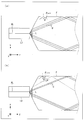
- FIG. 1 is a schematic diagram showing an outline of the alignment method according to the present embodiment.
- the alignment method according to the present embodiment is used in the alignment process included in the manufacturing method of the semiconductor laser module 10 as described above.
- a semiconductor laser module including a bottom plate 11 and submounts 12 to 13 in addition to the semiconductor laser element LD and the optical fiber F1 is assumed as the semiconductor laser module 10.
- the optical fiber F1 is a multimode fiber having a lens processed on an end face (hereinafter also referred to as an “incident end face”) facing the emission end face of the semiconductor laser element LD.
- the submount 12 is used as a base for mounting the semiconductor laser element LD.
- the submount 13 is used as a pedestal for placing the optical fiber F1.
- the optical fiber F1 is drawn into the semiconductor laser module 10 via an insertion pipe 14 provided on the side wall of the semiconductor laser module 10 and fixed (soldered or bonded) to the upper surface of the submount 13.
- the alignment method according to the present embodiment is performed after the step of drawing the optical fiber F1 into the semiconductor laser module 10 and before the step of fixing the optical fiber F1 to the upper surface of the submount 13.
- the alignment method includes (1) an insertion step of inserting a low NA optical fiber F2 having a numerical aperture lower than that of the optical fiber F1 into the output end face side of the optical fiber F1, and (2) a low NA optical fiber. And adjusting the position of the incident end face of the optical fiber F1 with respect to the exit end face of the semiconductor laser module LD so as to maximize the intensity with reference to the intensity of the light output from F2.
- the low NA optical fiber F2 functions as a wide-angle component removing unit that removes the wide-angle component from the light propagating through the optical fiber F1 and outputs the remaining narrow-angle component. Therefore, the adjustment process described above is performed with reference to a narrow-angle component in the light propagating through the optical fiber F1.
- one end face of the low NA optical fiber F2 (hereinafter also referred to as “incident end face”) is used as an outgoing end face of the optical fiber F1 (an end face opposite to the incident end face facing the outgoing end face of the semiconductor laser element LD).
- incident end face an end face opposite to the incident end face facing the outgoing end face of the semiconductor laser element LD.
- exit end face the intensity of light (narrow angle component) emitted from the other end face (hereinafter also referred to as “exit end face”) of the low NA optical fiber F2 is measured with the power meter PM,
- the incident end face is moved in the y-axis direction (direction perpendicular to the active layer of the semiconductor laser element LD).
- the position of the incident end face of the optical fiber F1 in the y-axis direction is matched with the position where the intensity of light emitted from the exit end face of the low NA optical fiber F2 is maximized.
- this invention is not limited to this.
- a configuration in which the optical fiber F1 is directly fixed to the bottom plate 11 may be employed.
- a configuration in which the semiconductor laser element LD is directly fixed to the bottom plate 11 may be employed.
- FIG. 2 is a diagram illustrating an optical path of light propagating through the optical fiber F1 and the low NA optical fiber F2.
- the optical fiber F1 propagates light whose propagation angle ⁇ is
- the low NA optical fiber F2 propagates light whose propagation angle ⁇ ′ is
- the low NA optical fiber F2 is an optical fiber having a lower numerical aperture than the optical fiber F1. Therefore, the critical angle ⁇ ′ that causes total reflection in the low NA optical fiber F2 is larger than the critical angle ⁇ that causes total reflection in the optical fiber F1.
- the wide-angle component that becomes crit ′ leaks from the side surface of the low NA optical fiber F2 without being confined in the low NA optical fiber F2.
- the function of the low NA optical fiber F2 can be expressed as follows. That is, the low NA optical fiber F2 removes a wide-angle component in which the propagation angle ⁇ in the optical fiber F1 is ⁇ crit ⁇ ⁇
- ⁇ ⁇ crit ⁇ is output from the emission end face.
- a solid line indicates an optical path corresponding to the narrow-angle component
- a dotted line indicates an optical path corresponding to the wide-angle component.
- the narrow angle component incident on the low NA optical fiber F2 is confined in the low NA optical fiber F2, as shown in FIG. 2, because the propagation angle ⁇ ′ in the low NA optical fiber F2 is
- the wide-angle component incident on the low NA optical fiber F2 has a propagation angle ⁇ ′ in the low NA optical fiber F2 of
- the dotted line is a tolerance curve of the optical output of the optical fiber F1 (the intensity of the light including both the wide-angle component and the narrow-angle component output from the output end face of the optical fiber F1)
- the solid line is a low NA
- It is a tolerance curve of the optical output of the optical fiber F2 (the intensity of light that is output from the output end face of the low NA optical fiber F2 and includes only the narrow-angle component).
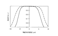
- the numerical aperture of the optical fiber F1 was 0.22
- the numerical aperture of the low NA optical fiber F2 was 0.15.
- the light propagating through the optical fiber F1 includes a wide-angle component. It comes to be.
- This wide-angle component is output from the output end face of the optical fiber F1 as long as the propagation angle ⁇ in the optical fiber F1 does not exceed the critical propagation angle ⁇ crit of the optical fiber 1. For this reason, even if the position of the incident end face of the optical fiber F1 deviates from the proper position, the intensity of light output from the exit end face of the optical fiber F1 hardly decreases. Therefore, the tolerance of the optical output of the optical fiber F1 is widened as shown by a dotted line in FIG.
- the tolerance of the output light of the low NA optical fiber F2 becomes narrower than the tolerance of the optical output of the optical fiber F1, as shown by a solid line in FIG. This is because, when the position of the incident end face of the optical fiber F1 deviates from the proper position, a wide angle component in which the propagation angle ⁇ ′ in the low NA optical fiber F2 exceeds the critical propagation angle ⁇ crit ′ of the low NA optical fiber F2 is low. This is because leakage occurs from the side surface of F2, and as a result, the intensity of light output from the emission end surface of the low NA optical fiber F2 decreases.
- the position of the incident end face of the optical fiber F1 is adjusted with reference to the light output of the low NA optical fiber F2, the position of the incident end face of the optical fiber F1 is adjusted with reference to the light output of the optical fiber F1.
- the low NA optical fiber F2 is used as the wide angle component removing means for removing the wide angle component from the light propagating through the optical fiber F1, but the present invention is not limited to this. That is, the low NA optical fiber F2 can be replaced with another optical system having a function of removing a wide-angle component from the light propagating through the optical fiber F1.
- the low NA optical fiber F2 can be replaced with another optical system having a function of removing a wide-angle component from the light propagating through the optical fiber F1.
- FIG. 4 is a schematic diagram showing an outline of the alignment method according to this modification.
- a spatial filter constituted by a lens L is used as a wide-angle component removing unit.
- the lens L is incident only on the light receiving surface of the power meter PM, of the light emitted from the emitting end face of the optical fiber F1, only the narrow-angle component in which the propagation angle ⁇ in the optical fiber F1 is
- ⁇ ⁇ crit is incident on the light receiving surface of the power meter PM. Without being removed (see the dotted line in FIG. 5).
- the alignment method according to the present embodiment is an alignment method for adjusting the relative position between the emission end face of the semiconductor laser element and the incident end face of the optical fiber, and the propagation angle propagates through the optical fiber.
- the wide angle component contained in the light propagating through the optical fiber is removed by the wide angle component removing means, and alignment based on the intensity of the remaining narrow angle component is performed. Therefore, according to the above configuration, the ratio of the narrow-angle component included in the light propagating through the optical fiber is increased as much as possible, that is, the ratio of the wide-angle component included in the light propagating through the optical fiber is as large as possible.
- the position of the incident end face of the optical fiber (relative position with respect to the emitting end face of the semiconductor laser element) can be adjusted so as to reduce the number.
- the only measurement required for alignment is the measurement of the intensity of the narrow-angle component output from the wide-angle component removal means, and no FFP measurement is required. Therefore, alignment capable of reducing the wide-angle component contained in the light propagating through the optical fiber can be realized with a simpler configuration than alignment based on FFP.
- the wide-angle component removing unit is another optical fiber connected to the emission end face of the optical fiber, and is another optical fiber having a lower numerical aperture than the optical fiber. Is preferable.
- the wide-angle component removing unit can be realized with a simple configuration at low cost.
- the optical fiber is preferably an optical fiber in which lens processing is performed on the incident end face.
- the alignment method may decrease in alignment accuracy due to the increased tolerance of the output light in the conventional alignment method.
- the alignment method according to the present invention since the spread of the tolerance of the output light can be suppressed, alignment with higher accuracy than the conventional alignment method can be realized.
- the method for manufacturing a semiconductor laser module according to the present embodiment is a method for manufacturing a semiconductor laser module including a semiconductor laser element and an optical fiber, and includes an emission end face of the semiconductor laser element and the light.
- the above alignment method is used.
- alignment capable of reducing the wide-angle component contained in the light propagating through the optical fiber can be realized with a simpler configuration than alignment based on FFP. Therefore, a semiconductor laser module capable of outputting light that does not include a wide-angle component that causes a loss in the combiner or the amplification fiber can be realized at low cost.
- the present invention can be widely applied to an alignment method for adjusting the relative position between the emission end face of the semiconductor laser element and the incident end face of the optical fiber.
- it can be suitably used for alignment in a semiconductor laser module.
Landscapes
- Physics & Mathematics (AREA)
- General Physics & Mathematics (AREA)
- Optics & Photonics (AREA)
- Condensed Matter Physics & Semiconductors (AREA)
- Electromagnetism (AREA)
- Optical Couplings Of Light Guides (AREA)
- Semiconductor Lasers (AREA)
Abstract
光ファイバ(F1)を伝搬する光から広角成分を除去する低NA光ファイバ(F2)を、光ファイバ(F1)の出射端面側に挿入する。そして、低NA光ファイバ(F2)から出力された狭角成分の強度を参照し、該強度を最大化するように半導体レーザ素子(LD)の出射端面に対する光ファイバ(F1)の入射端面の相対位置を調整する。
Description
本発明は、半導体レーザ素子の出射端面と光ファイバの入射端面との相対位置を調整する調心方法に関する。また、そのような調心方法を用いた調心工程を含む、半導体レーザモジュールの製造方法に関する。
ファイバレーザ等の光源装置として、半導体レーザモジュールが広く用いられている。半導体レーザモジュールは、その筐体内に設けられた半導体レーザ素子と、その筐体内に引き込まれた光ファイバとを備えている。半導体レーザ素子及び光ファイバは、半導体レーザモジュールの底板、又は、その底板上に設けられたサブマウントに固定される。
半導体レーザモジュールの製造に際しては、半導体レーザ素子の出射端面と光ファイバの入射端面との相対位置を結合効率が最大となるように調整すること(以下、「調心」とも記載)が重要になる。なぜなら、光ファイバに結合しなかった光は、光ファイバの被覆やメタライズを加熱し、焼損させる虞があるからである。なお、このメタライズは、光ファイバを底板又はサブマウントに半田付けする場合に必要となるものである。
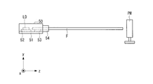
従来の調心方法の概要を図6に示す。図6に示す調心方法は、サブマウント52を介して底板51に固定された半導体レーザモジュールLDと、挿通パイプ54を介して引き込まれ、サブマウント53を介して底板51に固定された光ファイバFとを備えた半導体レーザモジュール50の製造に際して用いられる調心方法であり、光ファイバFをサブマウント53に固定する前に実施される。
半導体レーザ素子LDは、図6におけるzx平面に平行な活性層を有する端面発光型の半導体レーザ素子であり、半導体レーザ素子LDの出射端面から出射される光は、回折によりy軸方向に広がる。このため、光ファイバFの調心においては、特にy軸方向(半導体レーザ素子LDの活性層に直交する方向)の調心を精度良く行なうことが重要になる。
光ファイバFのy軸方向の調心は、光ファイバFの出射端面から出力される出力光の強度を参照して行われる。すなわち、光ファイバFの出力光の強度をパワーメータPMで測定しながら、光ファイバFの入射端面をy軸方向に移動する。そして、光ファイバFの入射端面のy軸方向の位置を、光ファイバFの出力光の強度が最大になる位置(以下、「適正位置」とも記載)に合わせる。
なお、光ファイバFの入射端面は、図8の(a)に示すように、yz平面に平行な断面が楔形になるように加工されており、稜線近傍の斜線を付した領域がレンズ部Lを構成している。半導体レーザ素子LDの活性層ALから出射された光は、このレンズ部Lを介し光ファイバFに入射する。光ファイバFに入射した光は、その伝搬角θが|θ|≦θcritであれば、光ファイバF内に閉じ込められ、光ファイバF内を伝搬する。ここで、θcritは、全反射を生じる臨界角をφとして、θcrit=90°-φにより定義される角度であり、本明細書ではこれを臨界伝搬角と呼ぶ。
このような調心方法を開示した文献としては、例えば、特許文献1~3などが挙げられる。
半導体レーザモジュールを構成する光ファイバを伝播する光に、その光ファイバの臨界伝搬角に近い伝搬角を有する成分(以下、「広角成分」とも記載)が含まれていると、その半導体レーザモジュールを備えたファイバレーザやファイバアンプの効率を悪化させたり、増幅用光ファイバの被覆を発熱させたりするといった問題を生じる。何故なら、半導体レーザモジュールを構成する光ファイバを伝播する光に含まれる広角成分は、その光ファイバに接続されるポンプコンバイナや増幅用ファイバにおける損失要因となるからである。したがって、半導体レーザモジュールを構成する光ファイバの調心においては、その光ファイバを伝播する光に含まれる広角成分を減少させるように、その光ファイバの入射端面の位置(半導体レーザ素子の出射端面に対する相対位置)を決定することが要求される。
しかしながら、光ファイバの入射端面の位置を、単に、その光ファイバの出射端面から出力される出力光の強度を参照して決定する構成では、この要求に応えることができない。何故なら、その光ファイバを伝播した光は、広角成分であるか狭角成分であるかの区別なくパワーメータに受光されるので、広角成分の多寡に応じて測定される出力光の強度が増減することはないからである。
また、光ファイバの入射端面の位置を、単に、その光ファイバの出射端面から出力される出力光の強度を参照して決定する構成では、図8の(a)に示すように入射端面がレンズ加工された光ファイバFを調心対象とする場合、精度の良い調心を実現することができないという問題を生じる。何故なら、図8の(b)に示すように、光ファイバFの入射端面がy軸方向に変位しても、図7の(a)に示すように、光ファイバFの出力光の強度が殆ど変化しない場合、すなわち、光出力(光ファイバFの出力光の強度)のトレランスが広がる場合があるためである。このように、光出力のトレランスが広がる理由は、以下のとおりである。
すなわち、図8の(b)に示すように、光ファイバFの入射端面がy軸方向に変位した場合、半導体レーザ素子LDの活性層ALから出射された光の一部は、図8の(b)に点線で示すように、レンズ部Lを介さずに光ファイバFに入射することになる。しかしながら、レンズ部Lを介さずに光ファイバFに入射した光も、その伝搬角θ’が|θ’|≦θcritであれば、レンズ部Lを介して光ファイバFに入射した光と同様、光ファイバF内に閉じ込められ、光ファイバF内を伝搬する。このため、光ファイバFの入射端面が適正位置から僅かに変位しても、光ファイバFの出力光の強度は、殆ど変化しない。
一方、図8の(b)に示すように、光ファイバFの入射端面がy軸方向に変位すると、光ファイバFを伝搬する光に、臨界伝搬角θcritに近い伝搬角を有する広角成分が含まれるようになる。この広角成分は、レンズ部Lを介さずに光ファイバFに入射した光により構成され、その伝搬角θ’は、光ファイバFのy軸方向への変位に略比例して大きくなる。このため、図7の(a)に示すように、光出力のトレンランスが広がる場合であっても、図7の(b)に示すように、最大伝搬角θmaxのトレランスは広がらない。ここで、最大伝搬角θmaxとは、実際に光ファイバFを伝搬する光(モード)のうち、最大の伝搬角を有する光(モード)の伝搬角のことを指す。
以上のように、入射端面にレンズ加工が施された光ファイバFの調心においては、光出力(光ファイバFの出力光の強度)のトレランスが広がる場合がある。この場合、光ファイバFの出力光の強度に基づく調心では、光ファイバFの入射端面の位置を真の適正位置に合わせることは困難である。そして、光ファイバFの入射端面の位置が真の適正位置から外れた場合、光ファイバFを伝搬する光に広角成分が含まれるようになる。
なお、光ファイバの出力光の強度に基づく調心に代えて、光ファイバの出力光のFFP(Far Field Pattern)に基づく調心を行なえば、上述した問題を回避することができる。しかしながら、FFPの測定には、複雑な装置が必要であり、時間的及び金銭的コストの上昇が避けられない。
本発明は、上記の問題に鑑みてなされたものであり、その目的は、半導体レーザ素子の出射端面と光ファイバの入射端面との相対位置を調整する調心方法において、その光ファイバの出力光の強度に基づきながらも、その光ファイバを伝播する光に含まれる広角成分を減少させ得る調心方法を実現することにある。
上記課題を解決するために、本発明に係る調心方法は、半導体レーザ素子の出射端面と光ファイバの入射端面との相対位置を調整する調心方法であって、上記光ファイバを伝搬する、伝搬角θが|θ|≦θcrit(θcritは上記光ファイバの臨界伝搬角)となる光から、伝搬角θがθcrit-δ<|θ|≦θcrit(δは正の定数)である広角成分を除去し、伝搬角θが|θ|≦θcrit-δである狭角成分を出力する広角成分除去手段を、上記光ファイバの出射端面側に挿入する挿入工程と、上記広角成分除去手段から出力された上記狭角成分の強度を参照し、該強度を最大化するように上記半導体レーザ素子の出射端面と上記光ファイバの入射端面との相対位置を調整する調整工程と、を含んでいる、ことを特徴とする。
本発明によれば、光ファイバを伝播する光に含まれる広角成分を減少させ得る調心を、FFPに基づく調心よりも簡単な構成で実現することができる。
本発明の一実施形態に係る調心方法について、図面に基づいて説明すれば以下のとおりである。
なお、本実施形態に係る調心方法は、半導体レーザモジュールの製造方法に含まれる調心工程において用いられるものであり、その半導体レーザモジュールを構成する半導体レーザ素子及び光ファイバを調心対象とする。ただし、本発明は、これに限定されるものではない。すなわち、本発明に係る調心方法は、半導体レーザ素子の出射端面と光ファイバの入射端面との相対位置を調整するものであればよく、調心対象とする半導体レーザ素子及び光ファイバが半導体レーザモジュールを構成するものであることを要さない。
〔調心方法の概要〕
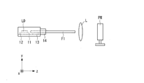
まず、本実施形態に係る調心方法の概要について、図1を参照して説明する。図1は、本実施形態に係る調心方法の概要を示す模式図である。
まず、本実施形態に係る調心方法の概要について、図1を参照して説明する。図1は、本実施形態に係る調心方法の概要を示す模式図である。
本実施形態に係る調心方法は、上述したように、半導体レーザモジュール10の製造方法に含まれる調心工程において用いられるものである。本実施形態においては、半導体レーザモジュール10として、半導体レーザ素子LDと、光ファイバF1とに加え、底板11と、サブマウント12~13とを備えた半導体レーザモジュールを想定する。光ファイバF1は、半導体レーザ素子LDの出射端面に対向する端面(以下「入射端面」とも記載)にレンズ加工が施されたマルチモードファイバである。
半導体レーザモジュール10において、サブマウント12は、半導体レーザ素子LDを載置するための台座として利用される。また、サブマウント13は、光ファイバF1を載置するための台座として利用される。光ファイバF1は、半導体レーザモジュール10の筐体側壁に設けられた挿通パイプ14を介して、半導体レーザモジュール10の内部に引き込まれ、サブマウント13の上面に固定(半田付け又は接着)される。本実施形態に係る調心方法は、光ファイバF1を半導体レーザモジュール10の内部に引き込む工程を実施した後、光ファイバF1をサブマウント13の上面に固定する工程を実施する前に実施される。
本実施形態に係る調心方法は、(1)光ファイバF1よりも開口数の低い低NA光ファイバF2を、光ファイバF1の出射端面側に挿入する挿入工程と、(2)低NA光ファイバF2から出力された光の強度を参照し、その強度を最大化するように半導体レーザモジュールLDの出射端面に対する光ファイバF1の入射端面の位置を調整する調整工程とを含む。ここで、低NA光ファイバF2は、光ファイバF1を伝搬する光から広角成分を除去し、残った狭角成分を出力する広角成分除去手段として機能する。したがって、上述した調整工程は、光ファイバF1を伝搬する光のうち、狭角成分を参照して実施される。
挿入工程においては、低NA光ファイバF2の一方の端面(以下「入射端面」とも記載)を、光ファイバF1の出射端面(半導体レーザ素子LDの出射端面と対向する入射端面と反対側の端面)に接続(例えば、融着)する。また、調整工程においては、低NA光ファイバF2の他方の端面(以下「出射端面」とも記載)から出射された光(狭角成分)の強度をパワーメータPMで測定しながら、光ファイバF1の入射端面をy軸方向(半導体レーザ素子LDの活性層に直交する方向)に移動する。そして、光ファイバF1の入射端面のy軸方向の位置を、低NA光ファイバF2の出射端面から出射された光の強度が最大になる位置に合わせる。
なお、本実施形態においては、光ファイバF1をサブマウント13を介して底板11に固定する構成を例示しているが、本発明はこれに限定されるものではない。例えば、光ファイバF1を底板11に直接固定する構成も採用してもよい。同様に、半導体レーザ素子LDを底板11に直接固定する構成を採用してもよい。
〔低NA光ファイバの機能〕
次に、低NA光ファイバF2の機能について、図2を参照して説明する。図2は、光ファイバF1及び低NA光ファイバF2を伝搬する光の光路を示す図である。
次に、低NA光ファイバF2の機能について、図2を参照して説明する。図2は、光ファイバF1及び低NA光ファイバF2を伝搬する光の光路を示す図である。
光ファイバF1は、伝搬角θが|θ|≦θcritとなる光を伝搬する。ここで、θcritは、光ファイバF1の臨界伝搬角であり、光ファイバF1において全反射を生じる臨界角をφとすると、θcrit=90°-φにより定義される角である。一方、低NA光ファイバF2は、伝搬角θ’が|θ’|≦θcrit’となる光を伝搬する。ここで、θcrit’は、低NA光ファイバF2の臨界伝搬角であり、低NA光ファイバF2において全反射を生じる臨界角をφ’とすると、θcrit’=90°-φ’により定義される角である。
ここで、低NA光ファイバF2は、光ファイバF1よりも開口数の低い光ファイバである。したがって、低NA光ファイバF2において全反射を生じる臨界角φ’は、光ファイバF1において全反射を生じる臨界角φよりも大きい。換言すれば、低NA光ファイバF2の臨界伝搬角θcrit’=90°-φ’は、光ファイバF1の臨界伝搬角θcritよりも小さい。したがって、光ファイバF1を伝搬する光(すなわち、光ファイバF1における伝搬角θが|θ|≦θcritとなる光)のうち、低NA光ファイバF2における伝搬角θ’が|θ’|>θcrit’となる広角成分は、低NA光ファイバF2に閉じ込められることなく、低NA光ファイバF2の側面から漏れ出す。
ここで、光ファイバF1を伝搬する光のうち、低NA光ファイバF2に入射したときに伝搬角がθcrit'となる光の伝搬角をθcrit”とし、δ=θcrit-θcrit”とすると、低NA光ファイバF2の機能は、以下のように表現することができる。すなわち、低NA光ファイバF2は、光ファイバF1を伝搬する光から、光ファイバF1における伝搬角θがθcrit-δ<|θ|≦θcritである広角成分を除去し、光ファイバF1における伝搬角θが|θ|≦θcrit-δである狭角成分を出射端面から出力する。なお、光ファイバF1のコアの屈折率と低NA光ファイバF2のコアの屈折率とが同一の場合、θcrit”=θcrit’であり、δ=θcrit-θcrit’となる。
図2において、実線は、上記狭角成分に対応する光路を示し、点線は、上記広角成分に対応する光路を示す。低NA光ファイバF2に入射した狭角成分は、低NA光ファイバF2における伝搬角θ’が|θ’|≦θcrit'となるので、図2に示すように、低NA光ファイバF2に閉じ込められ、低NA光ファイバF2の出射端面から出力される。一方、低NA光ファイバF2に入射した広角成分は、低NA光ファイバF2における伝搬角θ’が|θ’|>θcrit'となるので、図2に示すように、低NA光ファイバF2に閉じ込められることなく、低NA光ファイバF2の側面から外部に漏れ出す。したがって、低NA光ファイバF2に入射した光のうち、狭角成分のみが低NA光ファイバF2の出射端面から出射され、図1に示すパワーメータPMに入射することになる。
〔低NA光ファイバの効果〕
次に、低NA光ファイバ2の効果について、図3を参照して説明する。図3において、点線は、光ファイバF1の光出力(光ファイバF1の出射端面から出力される、広角成分及び狭角成分の両方を含む光の強度)のトレランスカーブであり、実線は、低NA光ファイバF2の光出力(低NA光ファイバF2の出射端面から出力される、狭角成分のみを含む光の強度)のトレンランスカーブである。なお、図3に示す各トレランスカーブの測定に際しては、光ファイバF1の開口数を0.22とし、低NA光ファイバF2の開口数を0.15とした。
次に、低NA光ファイバ2の効果について、図3を参照して説明する。図3において、点線は、光ファイバF1の光出力(光ファイバF1の出射端面から出力される、広角成分及び狭角成分の両方を含む光の強度)のトレランスカーブであり、実線は、低NA光ファイバF2の光出力(低NA光ファイバF2の出射端面から出力される、狭角成分のみを含む光の強度)のトレンランスカーブである。なお、図3に示す各トレランスカーブの測定に際しては、光ファイバF1の開口数を0.22とし、低NA光ファイバF2の開口数を0.15とした。
上述したように、入射端面にレンズ加工が施された光ファイバF1の調心においては、光ファイバF1の入射端面の位置が適正位置から外れると、光ファイバF1を伝搬する光に広角成分が含まれるようになる。この広角成分は、光ファイバF1における伝搬角θが光ファイバ1の臨界伝搬角θcritを超えない限り、光ファイバF1の出射端面から出力される。このため、光ファイバF1の入射端面の位置が適正位置から外れても、光ファイバF1の出射端面から出力される光の強度は殆ど低下しない。したがって、光ファイバF1の光出力のトレランスは、図3に点線で示すように広がったものとなる。
一方、低NA光ファイバF2の出力光のトレランスは、図3に実線で示すように、光ファイバF1の光出力のトレランスよりも狭くなる。これは、光ファイバF1の入射端面の位置が適正位置から外れると、低NA光ファイバF2における伝搬角θ’が低NA光ファイバF2の臨界伝搬角θcrit’を超える広角成分が低NA光ファイバF2の側面から漏れ出し、その結果、低NA光ファイバF2の出射端面から出力される光の強度が低下するからである。このため、低NA光ファイバF2の光出力を参照して光ファイバF1の入射端面の位置を調整すれば、光ファイバF1の光出力を参照して光ファイバF1の入射端面の位置を調整するよりも、精度の高い調心を行なうことが可能になる。
〔変形例〕
なお、本実施形態においては、光ファイバF1を伝搬する光から広角成分を除去する広角成分除去手段として低NA光ファイバF2を用いたが、本発明はこれに限定されるものではない。すなわち、低NA光ファイバF2は、光ファイバF1を伝搬する光から広角成分を除去する機能を有する他の光学系に置換することが可能である。以下、このような変形例について、図4及び図5を参照して簡単に説明する。
なお、本実施形態においては、光ファイバF1を伝搬する光から広角成分を除去する広角成分除去手段として低NA光ファイバF2を用いたが、本発明はこれに限定されるものではない。すなわち、低NA光ファイバF2は、光ファイバF1を伝搬する光から広角成分を除去する機能を有する他の光学系に置換することが可能である。以下、このような変形例について、図4及び図5を参照して簡単に説明する。
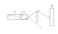
図4は、本変形例に係る調心方法の概要を示す模式図である。本変形例においては、図4に示すように、レンズLにより構成される空間フィルタを広角成分除去手段として用いている。
レンズLは、光ファイバF1の出射端面から出射された光のうち、光ファイバF1における伝搬角θが|θ|≦θcrit-δとなる狭角成分のみを、パワーメータPMの受光面に入射させるように設計されている(図5における実線参照)。一方、光ファイバF1の出射端面から出射された光のうち、光ファイバF1における伝搬角θがθcrit-δ<|θ|≦θcritとなる広角成分は、パワーメータPMの受光面に入射することなく、除去される(図5における点線参照)。
このように、広角成分除去手段として空間フィルタを用いた場合であっても、広角成分除去手段として低NA光ファイバ2を用いた場合と同様、精度の高い調心を行なうことができる。
〔まとめ〕
以上のように、本実施形態に係る調心方法は、半導体レーザ素子の出射端面と光ファイバの入射端面との相対位置を調整する調心方法であって、上記光ファイバを伝搬する、伝搬角θが|θ|≦θcrit(θcritは上記光ファイバの臨界伝搬角)となる光から、伝搬角θがθcrit-δ<|θ|≦θcrit(δは正の定数)である広角成分を除去し、伝搬角θが|θ|≦θcrit-δである狭角成分を出力する広角成分除去手段を、上記光ファイバの出射端面側に挿入する挿入工程と、上記広角成分除去手段から出力された上記狭角成分の強度を参照し、該強度を最大化するように上記半導体レーザ素子の出射端面と上記光ファイバの入射端面との相対位置を調整する調整工程と、を含んでいる、ことを特徴とする。
以上のように、本実施形態に係る調心方法は、半導体レーザ素子の出射端面と光ファイバの入射端面との相対位置を調整する調心方法であって、上記光ファイバを伝搬する、伝搬角θが|θ|≦θcrit(θcritは上記光ファイバの臨界伝搬角)となる光から、伝搬角θがθcrit-δ<|θ|≦θcrit(δは正の定数)である広角成分を除去し、伝搬角θが|θ|≦θcrit-δである狭角成分を出力する広角成分除去手段を、上記光ファイバの出射端面側に挿入する挿入工程と、上記広角成分除去手段から出力された上記狭角成分の強度を参照し、該強度を最大化するように上記半導体レーザ素子の出射端面と上記光ファイバの入射端面との相対位置を調整する調整工程と、を含んでいる、ことを特徴とする。
上記の構成によれば、上記光ファイバを伝播する光に含まれる広角成分が上記広角成分除去手段によって除去され、残った狭角成分の強度に基づく調心が行なわれる。このため、上記の構成によれば、上記光ファイバを伝播する光に含まれる狭角成分の割合ができるだけ多くなるように、すなわち、上記光ファイバを伝播する光に含まれる広角成分の割合ができるだけ少なくなるように、上記光ファイバの入射端面の位置(上記半導体レーザ素子の出射端面に対する相対位置)を調整することができる。
しかも、上記の構成によれば、調心のために必要な測定は、上記広角成分除去手段から出力された上記狭角成分の強度の測定のみであり、FFPの測定を要さない。したがって、上記光ファイバを伝播する光に含まれる広角成分を減少させ得る調心を、FFPに基づく調心よりも簡単な構成で実現することができる。
本実施形態に係る調心方法において、上記広角成分除去手段は、上記光ファイバの出射端面に接続された他の光ファイバであって、上記光ファイバよりも開口数の低い他の光ファイバである、ことが好ましい。
上記の構成によれば、上記広角成分除去手段を、簡単な構成で安価に実現することができる。
本実施形態に係る調心方法において、上記光ファイバは、上記入射端面にレンズ加工が施された光ファイバであることが好ましい。
調心対象となる光ファイバの入射端面にレンズ加工が施されている場合、従来の調心方法では出力光のトレランスが広がることに伴う調心精度の低下が生じ得る。これに対し、本発明に係る調心方法によれば、出力光のトレランスの広がりを抑えることができるので、従来の調心方法よりも精度の良い調心を実現することができる。
また、以上のように、本実施形態に係る半導体レーザモジュールの製造方法は、半導体レーザ素子と光ファイバとを備えた半導体レーザモジュールの製造方法であって、上記半導体レーザ素子の出射端面と上記光ファイバの入射端面との相対位置を調整する調心工程において、上記調心方法を用いることを特徴とする。
上記の構成によれば、上記光ファイバを伝播する光に含まれる広角成分を減少させ得る調心を、FFPに基づく調心よりも簡単な構成で実現することができる。このため、コンバイナや増幅用ファイバにおける損失要因になる広角成分を含まない光を出力することが可能な半導体レーザモジュールを安価に実現することができる。
〔付記事項〕
本発明は上述した実施形態に限定されるものではなく、請求項に示した範囲で種々の変更が可能である。すなわち、請求項に示した範囲で適宜変更した技術的手段を組み合わせて得られる実施形態についても本発明の技術的範囲に含まれる。
本発明は上述した実施形態に限定されるものではなく、請求項に示した範囲で種々の変更が可能である。すなわち、請求項に示した範囲で適宜変更した技術的手段を組み合わせて得られる実施形態についても本発明の技術的範囲に含まれる。
本発明は、半導体レーザ素子の出射端面と光ファイバの入射端面との相対位置を調整する調心方法に広く適用することができる。特に、半導体レーザモジュールにおける調心に好適に利用することができる。
10 半導体レーザモジュール
11 底板
12 サブマウント(LD用)
13 サブマウント(光ファイバ用)
14 挿通パイプ
LD 半導体レーザ素子
F1 光ファイバ
F2 低NA光ファイバ(他の光ファイバ)
PM パワーメータ
11 底板
12 サブマウント(LD用)
13 サブマウント(光ファイバ用)
14 挿通パイプ
LD 半導体レーザ素子
F1 光ファイバ
F2 低NA光ファイバ(他の光ファイバ)
PM パワーメータ
Claims (4)
- 半導体レーザ素子の出射端面と光ファイバの入射端面との相対位置を調整する調心方法であって、
上記光ファイバを伝搬する、伝搬角θが|θ|≦θcrit(θcritは上記光ファイバの臨界伝搬角)となる光から、伝搬角θがθcrit-δ<|θ|≦θcrit(δは正の定数)である広角成分を除去し、伝搬角θが|θ|≦θcrit-δである狭角成分を出力する広角成分除去手段を、上記光ファイバの出射端面側に挿入する挿入工程と、
上記広角成分除去手段から出力された上記狭角成分の強度を参照し、該強度を最大化するように上記半導体レーザ素子の出射端面と上記光ファイバの入射端面との相対位置を調整する調整工程と、を含んでいる、
ことを特徴とする調心方法。 - 上記広角成分除去手段は、上記光ファイバの出射端面に接続された他の光ファイバであって、上記光ファイバよりも開口数の低い他の光ファイバである、
ことを特徴とする請求項1に記載の調心方法。 - 上記光ファイバは、上記入射端面にレンズ加工が施された光ファイバである、
ことを特徴とする請求項1又は2に記載の調心方法。 - 半導体レーザ素子と光ファイバとを備えた半導体レーザモジュールの製造方法であって、
上記半導体レーザ素子の出射端面と上記光ファイバの入射端面との相対位置を調整する調心工程において、請求項1から3までの何れか1項に記載の調心方法を用いる、
ことを特徴とする半導体レーザモジュールの製造方法。
Applications Claiming Priority (2)
| Application Number | Priority Date | Filing Date | Title |
|---|---|---|---|
| JP2012063756A JP2013197372A (ja) | 2012-03-21 | 2012-03-21 | 調心方法及び半導体レーザモジュールの製造方法 |
| JP2012-063756 | 2012-03-21 |
Publications (1)
| Publication Number | Publication Date |
|---|---|
| WO2013140687A1 true WO2013140687A1 (ja) | 2013-09-26 |
Family
ID=49222173
Family Applications (1)
| Application Number | Title | Priority Date | Filing Date |
|---|---|---|---|
| PCT/JP2012/082639 Ceased WO2013140687A1 (ja) | 2012-03-21 | 2012-12-17 | 調心方法及び半導体レーザモジュールの製造方法 |
Country Status (2)
| Country | Link |
|---|---|
| JP (1) | JP2013197372A (ja) |
| WO (1) | WO2013140687A1 (ja) |
Families Citing this family (1)
| Publication number | Priority date | Publication date | Assignee | Title |
|---|---|---|---|---|
| JP7126062B2 (ja) * | 2016-12-06 | 2022-08-26 | パナソニックIpマネジメント株式会社 | 調芯方法 |
Citations (4)
| Publication number | Priority date | Publication date | Assignee | Title |
|---|---|---|---|---|
| JPH07283425A (ja) * | 1994-04-07 | 1995-10-27 | Hitachi Ltd | 光送受信モジュール |
| JPH10332985A (ja) * | 1997-05-27 | 1998-12-18 | Canon Inc | レンズの位置調整に用いる治具及びそれを用いたレンズ位置調整方法 |
| JPH1158665A (ja) * | 1997-08-27 | 1999-03-02 | Asahi Chem Ind Co Ltd | レーザ製版装置 |
| JP2012042819A (ja) * | 2010-08-20 | 2012-03-01 | Fujikura Ltd | レーザダイオードモジュール及びレーザ光源 |
-
2012
- 2012-03-21 JP JP2012063756A patent/JP2013197372A/ja active Pending
- 2012-12-17 WO PCT/JP2012/082639 patent/WO2013140687A1/ja not_active Ceased
Patent Citations (4)
| Publication number | Priority date | Publication date | Assignee | Title |
|---|---|---|---|---|
| JPH07283425A (ja) * | 1994-04-07 | 1995-10-27 | Hitachi Ltd | 光送受信モジュール |
| JPH10332985A (ja) * | 1997-05-27 | 1998-12-18 | Canon Inc | レンズの位置調整に用いる治具及びそれを用いたレンズ位置調整方法 |
| JPH1158665A (ja) * | 1997-08-27 | 1999-03-02 | Asahi Chem Ind Co Ltd | レーザ製版装置 |
| JP2012042819A (ja) * | 2010-08-20 | 2012-03-01 | Fujikura Ltd | レーザダイオードモジュール及びレーザ光源 |
Also Published As
| Publication number | Publication date |
|---|---|
| JP2013197372A (ja) | 2013-09-30 |
Similar Documents
| Publication | Publication Date | Title |
|---|---|---|
| US10746933B2 (en) | Fiber coupled laser source pump with wavelength division multiplexer, isolator, tap filter, and photodetector | |
| JP6420237B2 (ja) | 高性能空間フィルタ | |
| US9224929B2 (en) | Optical semiconductor device and manufacturing method therefor | |
| US6668112B1 (en) | Multimode laser diode and side-coupled fiber package | |
| WO2024066048A1 (zh) | 光路耦合组件及带有光路耦合组件的光模块 | |
| JP7504702B2 (ja) | 半導体レーザ装置及びレーザ装置 | |
| JPH03140912A (ja) | 反射軽減集成装置 | |
| JP5420388B2 (ja) | 光モジュール、光モジュールの製造方法及び光モジュールの調整方法 | |
| CN118295086B (zh) | 具有波分复用器的光纤耦合激光源泵浦 | |
| US7251394B2 (en) | Optical isolator with tilted optical isolator element | |
| JP2020134609A (ja) | 光学素子 | |
| JP6540310B2 (ja) | 光ファイバ端末 | |
| JP2013197372A (ja) | 調心方法及び半導体レーザモジュールの製造方法 | |
| JP2005134803A (ja) | 光アイソレータ付きフェルール及びそれを備えた光送受信モジュール | |
| JP2010066562A (ja) | 光ファイバ位置決め方法 | |
| JP7623613B2 (ja) | 光モジュール、調芯システム及び光計測方法 | |
| JP2006276507A (ja) | ファラデー回転ミラー | |
| JP6010892B2 (ja) | 平面導波路型レーザ装置 | |
| EP2637052B1 (en) | Optical coupling structure and array optical amplification module | |
| US20200183102A1 (en) | Light guide body, optical module, and optical path and optical axis adjustment method | |
| JP4764654B2 (ja) | 光モジュール | |
| JP2005331762A (ja) | 光モニタならびにそれを用いた光モニタアレイおよび光システム | |
| JP2008003211A (ja) | インライン型ハイブリッド光デバイス | |
| JP2002124723A (ja) | 光結合器 | |
| CN120415574A (zh) | 一种集成化多通道掺铒放大光源装置与封装方法 |
Legal Events
| Date | Code | Title | Description |
|---|---|---|---|
| 121 | Ep: the epo has been informed by wipo that ep was designated in this application |
Ref document number: 12872087 Country of ref document: EP Kind code of ref document: A1 |
|
| NENP | Non-entry into the national phase |
Ref country code: DE |
|
| 122 | Ep: pct application non-entry in european phase |
Ref document number: 12872087 Country of ref document: EP Kind code of ref document: A1 |