WO2013157350A1 - 電力変換回路 - Google Patents
電力変換回路 Download PDFInfo
- Publication number
- WO2013157350A1 WO2013157350A1 PCT/JP2013/058342 JP2013058342W WO2013157350A1 WO 2013157350 A1 WO2013157350 A1 WO 2013157350A1 JP 2013058342 W JP2013058342 W JP 2013058342W WO 2013157350 A1 WO2013157350 A1 WO 2013157350A1
- Authority
- WO
- WIPO (PCT)
- Prior art keywords
- switching
- switching element
- switching elements
- input terminal
- side input
- Prior art date
- Legal status (The legal status is an assumption and is not a legal conclusion. Google has not performed a legal analysis and makes no representation as to the accuracy of the status listed.)
- Ceased
Links
Images
Classifications
-
- H—ELECTRICITY
- H02—GENERATION; CONVERSION OR DISTRIBUTION OF ELECTRIC POWER
- H02M—APPARATUS FOR CONVERSION BETWEEN AC AND AC, BETWEEN AC AND DC, OR BETWEEN DC AND DC, AND FOR USE WITH MAINS OR SIMILAR POWER SUPPLY SYSTEMS; CONVERSION OF DC OR AC INPUT POWER INTO SURGE OUTPUT POWER; CONTROL OR REGULATION THEREOF
- H02M7/00—Conversion of AC power input into DC power output; Conversion of DC power input into AC power output
- H02M7/42—Conversion of DC power input into AC power output without possibility of reversal
- H02M7/44—Conversion of DC power input into AC power output without possibility of reversal by static converters
- H02M7/48—Conversion of DC power input into AC power output without possibility of reversal by static converters using discharge tubes with control electrode or semiconductor devices with control electrode
- H02M7/53—Conversion of DC power input into AC power output without possibility of reversal by static converters using discharge tubes with control electrode or semiconductor devices with control electrode using devices of a triode or transistor type requiring continuous application of a control signal
- H02M7/537—Conversion of DC power input into AC power output without possibility of reversal by static converters using discharge tubes with control electrode or semiconductor devices with control electrode using devices of a triode or transistor type requiring continuous application of a control signal using semiconductor devices only, e.g. single switched pulse inverters
- H02M7/5387—Conversion of DC power input into AC power output without possibility of reversal by static converters using discharge tubes with control electrode or semiconductor devices with control electrode using devices of a triode or transistor type requiring continuous application of a control signal using semiconductor devices only, e.g. single switched pulse inverters in a bridge configuration
- H02M7/53871—Conversion of DC power input into AC power output without possibility of reversal by static converters using discharge tubes with control electrode or semiconductor devices with control electrode using devices of a triode or transistor type requiring continuous application of a control signal using semiconductor devices only, e.g. single switched pulse inverters in a bridge configuration with automatic control of output voltage or current
-
- H—ELECTRICITY
- H02—GENERATION; CONVERSION OR DISTRIBUTION OF ELECTRIC POWER
- H02M—APPARATUS FOR CONVERSION BETWEEN AC AND AC, BETWEEN AC AND DC, OR BETWEEN DC AND DC, AND FOR USE WITH MAINS OR SIMILAR POWER SUPPLY SYSTEMS; CONVERSION OF DC OR AC INPUT POWER INTO SURGE OUTPUT POWER; CONTROL OR REGULATION THEREOF
- H02M7/00—Conversion of AC power input into DC power output; Conversion of DC power input into AC power output
- H02M7/42—Conversion of DC power input into AC power output without possibility of reversal
- H02M7/44—Conversion of DC power input into AC power output without possibility of reversal by static converters
- H02M7/48—Conversion of DC power input into AC power output without possibility of reversal by static converters using discharge tubes with control electrode or semiconductor devices with control electrode
- H02M7/53—Conversion of DC power input into AC power output without possibility of reversal by static converters using discharge tubes with control electrode or semiconductor devices with control electrode using devices of a triode or transistor type requiring continuous application of a control signal
- H02M7/537—Conversion of DC power input into AC power output without possibility of reversal by static converters using discharge tubes with control electrode or semiconductor devices with control electrode using devices of a triode or transistor type requiring continuous application of a control signal using semiconductor devices only, e.g. single switched pulse inverters
- H02M7/538—Conversion of DC power input into AC power output without possibility of reversal by static converters using discharge tubes with control electrode or semiconductor devices with control electrode using devices of a triode or transistor type requiring continuous application of a control signal using semiconductor devices only, e.g. single switched pulse inverters in a push-pull configuration
-
- H—ELECTRICITY
- H02—GENERATION; CONVERSION OR DISTRIBUTION OF ELECTRIC POWER
- H02M—APPARATUS FOR CONVERSION BETWEEN AC AND AC, BETWEEN AC AND DC, OR BETWEEN DC AND DC, AND FOR USE WITH MAINS OR SIMILAR POWER SUPPLY SYSTEMS; CONVERSION OF DC OR AC INPUT POWER INTO SURGE OUTPUT POWER; CONTROL OR REGULATION THEREOF
- H02M7/00—Conversion of AC power input into DC power output; Conversion of DC power input into AC power output
- H02M7/42—Conversion of DC power input into AC power output without possibility of reversal
- H02M7/44—Conversion of DC power input into AC power output without possibility of reversal by static converters
- H02M7/48—Conversion of DC power input into AC power output without possibility of reversal by static converters using discharge tubes with control electrode or semiconductor devices with control electrode
- H02M7/53—Conversion of DC power input into AC power output without possibility of reversal by static converters using discharge tubes with control electrode or semiconductor devices with control electrode using devices of a triode or transistor type requiring continuous application of a control signal
- H02M7/537—Conversion of DC power input into AC power output without possibility of reversal by static converters using discharge tubes with control electrode or semiconductor devices with control electrode using devices of a triode or transistor type requiring continuous application of a control signal using semiconductor devices only, e.g. single switched pulse inverters
- H02M7/5387—Conversion of DC power input into AC power output without possibility of reversal by static converters using discharge tubes with control electrode or semiconductor devices with control electrode using devices of a triode or transistor type requiring continuous application of a control signal using semiconductor devices only, e.g. single switched pulse inverters in a bridge configuration
Definitions
- the present invention relates to a bridge-type power conversion circuit that converts DC power into AC power.
- Non-Patent Document 1 discloses a single-phase inverter and a three-phase inverter as this type of bridge-type inverter.
- the single-phase bridge inverter includes first and second switching elements connected in series between a high voltage side input terminal and a low voltage side input terminal, and a high voltage side input terminal and a low voltage side input terminal. And a third switching element and a fourth switching element connected in series.
- This single-phase bridge inverter has an intermediate node between the first and second switching elements by alternately turning on the first and fourth switching elements and the second and third switching elements. And single-phase AC power between the third switching element and the intermediate node of the third and fourth switching elements (for example, FIGS. 6 and 9).
- the three-phase bridge inverter includes first and second switching elements connected in series between a high voltage side input terminal and a low voltage side input terminal, a high voltage side input terminal, and a low voltage side input terminal. And third and fourth switching elements connected in series in sequence between the first and second switching elements, and fifth and sixth switching elements connected in series in order between the high voltage side input terminal and the low voltage side input terminal, Is provided.
- This three-phase bridge inverter for example, combines a set of first and fourth switching elements, a set of third and sixth switching elements, and a set of fifth and second switching elements with a 1/3 period.
- the intermediate node of the first and second switching elements, the intermediate node of the third and fourth switching elements, and the intermediate node of the fifth and sixth switching elements And three-phase AC power is generated between them (for example, FIGS. 7 and 10).
- Non-Patent Document 1 also discloses a bridge-type inverter that performs switching control using a pulse width modulation (PWM) method during a period in which each set of switching elements is in an on state ( For example, FIG.
- PWM pulse width modulation
- an object of the present invention is to provide a power conversion circuit capable of reducing the price.
- the power conversion circuit of the present invention is connected in series between the high voltage side input terminal and the low voltage side input terminal in order, and the first and second intermediate nodes are connected to the first output terminal.
- a switching element, and a third and a fourth switching element connected in series between the high-voltage side input terminal and the low-voltage side input terminal, and having an intermediate node connected to the second output terminal.
- the first and fourth switching elements and the second and third switching elements are alternately turned on to input between the high voltage side input terminal and the low voltage side input terminal.
- a bridge-type power conversion circuit that converts direct-current power generated to generate alternating-current power between first and second output terminals, the first and third switching elements and the second and fourth Any one of a set of switching elements Controlling switching of the set at a higher frequency than the other set.
- one of the first and third switching elements and the second and fourth switching elements is subjected to switching control at a higher frequency than the other.
- a switching element having a relatively low operating speed and a low price can be used as the other set of switching elements. Therefore, according to this power conversion circuit, the price can be reduced.
- a CMOSFET Complementary Metal Oxide Semiconductor Field Effect Transistor
- PMOSFET P-channel Metal Oxide Semiconductor Field Effect Transistor
- NMOSFET N-channel
- Metal Oxide Semiconductor Field Effect Transistor may be used. While the CMOSFET has an advantage that it can be easily driven by a clock signal, the PMOSFET tends to be slower in operation speed than the NMOSFET, and has a problem that it is difficult to increase the switching control speed.
- the switching control of the second and fourth switching elements on the lower arm side is performed at a higher frequency than the first and third switching elements on the upper arm side, it is suitable when a CMOSFET is used as the switching element. In addition, it is possible to obtain both high speed switching control and easy driving of the switching element.
- the first switching element is turned on and the pulse width modulation method is used in the half cycle period of the AC power in which the first and fourth switching elements are turned on. And using the fourth switching element to control the switching, and in the other half-cycle period of the AC power to turn on the set of the second and third switching elements, the third switching element is turned on, It is preferable to control the switching of the second switching element using a pulse width modulation method.
- the switching of the first switching element is controlled using the pulse width modulation method during the half cycle period of the AC power in which the first and fourth switching elements are turned on.
- AC power that controls the switching of the fourth switching element at a frequency that is twice or more the switching frequency of the first switching element by using the pulse width modulation method, and turns on the set of the second and third switching elements.
- the third switching element is subjected to switching control using the pulse width modulation method, and the second switching frequency of the third switching element is set to a frequency that is twice or more the switching frequency of the third switching element using the pulse width modulation method. It is preferable to perform switching control of the two switching elements.
- the first to fourth switching elements are subjected to switching control so as to generate single-phase AC power between the first and second output terminals. According to this, it is possible to realize a low-cost full-bridge type single-phase inverter circuit.
- the fifth and sixth terminals are connected in series between the high voltage side input terminal and the low voltage side input terminal in order, and the intermediate node is connected to the third output terminal.
- Switching elements, and any one of the first, third, and fifth switching elements and the second, fourth, and sixth switching elements is higher than the other.
- the first to sixth switching elements are preferably subjected to switching control so that switching control is performed at a frequency and three-phase AC power is generated between the first to third output terminals. According to this, a low-cost bridge-type three-phase inverter circuit can be realized.
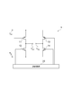
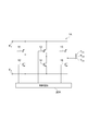
- FIG. 1 is a circuit diagram showing a single-phase full-bridge type inverter according to a first embodiment of the present invention.
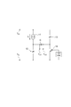
- FIG. 2 is a diagram illustrating an equivalent circuit of the inverter according to the first embodiment during a period in which the first switching element is in the on state.
- FIG. 3 is a diagram illustrating an equivalent circuit of the inverter of the first embodiment during a period in which the third switching element is in the on state.
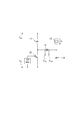
- FIG. 4 is a diagram illustrating the output voltage of the inverter according to the first embodiment during a period in which the first switching element is in the on state.
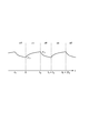
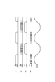
- FIG. 5 is a diagram illustrating an output AC voltage of the inverter according to the first embodiment.
- FIG. 6 is a circuit diagram showing a single-phase bridge type inverter according to the second embodiment of the present invention.
- FIG. 1 is a circuit diagram showing an inverter according to the first embodiment of the present invention.
- the inverter (power conversion circuit) 1 of the first embodiment is a single-phase full-bridge type inverter.
- the inverter 1 converts DC power input between the high voltage side input terminal T IH and the low voltage side input terminal T IL to provide a simple connection between the first and second output terminals T O1 and T O2. Generate phase AC power.
- the inverter 1 includes first to fourth switching elements 11 to 14 and a control circuit 20.
- the first and second switching elements 11 and 12 are sequentially connected in series between the high voltage side input terminal T IH and the low voltage side input terminal T IL, and these intermediate nodes serve as the first output terminal. Connected to TO1 .
- the first switching element 11 on the upper arm side is a PMOSFET
- the second switching element 12 on the lower arm side is an NMOSFET.
- the source terminal of the first switching element 11 is connected to the high-voltage side input terminal TIH
- the drain terminal is connected to the drain terminal of the second switching element 12.
- the source terminal of the second switching element 12 is connected to the low voltage side input terminal TIL .
- the drain terminals of the first and second switching elements 11 and 12 are connected to the first output terminal TO1 .
- the gate terminals of the first and second switching elements 11 and 12 are connected to the control circuit 20.
- the third and fourth switching elements 13 and 14 are sequentially connected in series between the high voltage side input terminal T IH and the low voltage side input terminal T IL, and these intermediate nodes are connected to the second node.
- the third switching element 13 on the upper arm side is a PMOSFET
- the fourth switching element 14 on the lower arm side is an NMOSFET.
- the source terminal of the third switching element 13 is connected to the high voltage side input terminal TIH
- the drain terminal is connected to the drain terminal of the fourth switching element 14.
- the source terminal of the fourth switching element 14 is connected to the low voltage side input terminal TIL .
- the drain terminals of the third and fourth switching elements 13 and 14 are connected to the second output terminal TO2 .
- the gate terminals of the third and fourth switching elements 13 and 14 are connected to the control circuit 20.
- the control circuit 20 performs switching control of the first to fourth switching elements 11 to 14. Specifically, the control circuit 20 turns on a set of the first and fourth switching elements 11 and 14 and a set of the second and third switching elements 12 and 13 alternately to turn on the high DC power input between the voltage side input terminal T IH and the low voltage side input terminal T IL is converted to generate single-phase AC power between the first and second output terminals T O1 and T O2. .
- control circuit 20 turns on the first switching element 11 during a half cycle period of the output single-phase AC power in which the pair of the first and fourth switching elements 11 and 14 is turned on. And switching control of the fourth switching element 14 using a pulse width modulation (PWM) method.
- PWM pulse width modulation
- control circuit 20 turns on the third switching element 13 in the other half-cycle period of the output single-phase AC power that turns on the pair of the second and third switching elements 12 and 13.
- the second switching element 12 is subjected to switching control using the PWM method.
- control circuit 20 performs switching control of the first and third switching elements 11 and 13 on the upper arm side at the frequency of the output AC power, and controls the second and fourth switching elements 12 and 14 on the lower arm side. Switching control is performed at a frequency higher than that of the first and third switching elements 11 and 13 using the PWM method.
- the operation of the inverter 1 of the first embodiment will be described.
- the first switching element 11 and the third switching element 13 are alternately on / off controlled at a low speed (for example, a frequency of 60 Hz).
- the fourth switching element 14 is PWM-controlled at a high speed (for example, 120 kHz)
- the third switching element 13 is in the on state.
- the switching element 12 is PWM-controlled at a high speed (for example, 120 kHz).
- FIG. 2 is a diagram showing an equivalent circuit of the inverter 1 during the period in which the first switching element 11 is in the on state
- FIG. 3 is an equivalent circuit of the inverter 1 during the period in which the third switching element 13 is in the on state.
- a smoothing capacitor (capacitance value C) is connected between the first and second output terminals T O1 and T O2 in order to facilitate the following description of the operation. To do. Further, it is assumed that a resistive load (resistance value R) is connected between the first and second output terminals T O1 and T O2 .
- i S in FIGS. 2 and 3 is the saturation current value of each of the first and third switching elements 11 and 13.
- FIG. 4 is a diagram illustrating the output voltage of the inverter 1 during the period in which the first switching element 11 is in the on state.
- the time when the fourth switching element 14 switches from the off state to the on state is the origin, the off time is t 1 , and the on time is t 2 . That is, one cycle of on-off switching is t 1 + t 2 .
- FIG. 5 is a diagram showing the output voltage of the inverter 1.
- FIG. 5 also shows the on state-off state of the first to fourth switching elements 11-14.
- the second and third switching elements 12 and 13 are held in the off state during the period in which the first switching element 11 is in the on state.
- the fourth switching element 14 is PWM-controlled at 120 kHz, for example.
- the above equations (1) and (2) are one-stage linear ordinary differential equations.
- the general solution of the above equation (1) is obtained as the following equation (3), and the general solution of the above equation (2) is It is calculated as shown in (4).
- ⁇ is a voltage decay constant, that is, the reciprocal 1 / CR of the CR time constant
- v 0 and v 1 are integration constants determined from voltage continuity conditions on the time axis described below.
- the coefficient ⁇ t 2 / (t 1 + t 2 ) is a ratio of the on period to one cycle of on / off switching of the fourth switching element 14, and is called a switching duty ratio.
- a desired output voltage can be obtained by controlling the duty ratio of the fourth switching 14.
- the first and fourth switching elements 11 and 14 are held in the off state during the period in which the third switching element 13 is in the on state.
- the second switching element 12 is PWM-controlled at 120 kHz, for example.
- the output voltage waveform in the period in which the third switching element 13 is in the on state has the opposite polarity to the output voltage waveform in the period in which the first switching element 11 is in the on state.
- the lower arm side second and fourth switching elements 12 and 14 are higher than the upper arm side first and third switching elements 11 and 13.
- the first arm and the third switching elements 11 and 13 on the upper arm side can use switching elements with relatively low operating speed and low cost.
- the driving circuit for the first and third switching elements 11 and 13 on the upper arm side can be configured to be relatively slow in operation speed and low in cost. Therefore, according to the inverter 1 of the first embodiment, the price can be reduced.
- the switching element on the upper arm side is also composed of an NMOSFET.
- NMOSFET an insulating device such as a photocoupler is required for the drive circuit of the NMOSFET on the upper arm side, and there is a problem that the driving easiness of the switching element is impaired and the cost reduction is difficult.
- the inverter 1 of the first embodiment it is suitable when a CMOSFET is used as a switching element, and it is possible to obtain high speed switching control, easy driving of the switching element, and low cost. Become. [Second Embodiment]
- FIG. 6 is a circuit diagram showing an inverter according to the second embodiment of the present invention.
- the inverter (power conversion circuit) 1A of the second embodiment is a three-phase bridge type inverter.
- the inverter 1A converts the DC power input between the high voltage side input terminal T IH and the low voltage side input terminal T IL to convert the first to third output terminals T O1 , T O2 , T O3 . Three-phase AC power is generated between them.
- This inverter 1A is different from the first embodiment in that the inverter 1 further includes fifth and sixth switching elements 15 and 16 and a control circuit 20A instead of the control circuit 20.
- the fifth and sixth switching elements 15 and 16 are sequentially connected in series between the high voltage side input terminal T IH and the low voltage side input terminal T IL, and these intermediate nodes serve as the third output terminal. Connected to TO3 .
- the upper arm side fifth switching element 15 is a PMOSFET
- the lower arm side sixth switching element 16 is an NMOSFET.
- the source terminal of the fifth switching element 15 is connected to the high voltage side input terminal TIH , and the drain terminal is connected to the drain terminal of the sixth switching element 16.
- the source terminal of the sixth switching element 16 is connected to the low voltage side input terminal TIL .
- the drain terminals of the fifth and sixth switching elements 15 and 16 are connected to the third output terminal TO3 .
- the gate terminals of the fifth and sixth switching elements 15 and 16 are connected to the control circuit 20A.
- the control circuit 20A performs switching control of the first to sixth switching elements 11 to 16.
- the control circuit 20A includes a set of first and fourth switching elements 11 and 14, a set of third and sixth switching elements 13 and 16, and a set of fifth and second switching elements 15 and 12. Are shifted by 1/3 period and turned on to convert the DC power input between the high voltage side input terminal T IH and the low voltage side input terminal T IL to convert the first to third Three-phase AC power is generated between the output terminals T O1 to T O3 .
- control circuit 20A turns on the first switching element 11 during the period of 1/3 cycle of the output three-phase AC power, and sets the fourth switching element 14 using the PWM method. Control switching. Further, the control circuit 20A turns on the third switching element 13 and controls the switching of the sixth switching element 16 using the PWM method in the other one-third period of the output three-phase AC power. To do. In addition, the control circuit 20A turns on the fifth switching element 15 and switches the second switching element 12 using the PWM method in another 1/3 cycle period of the output three-phase AC power. Control.
- control circuit 20A performs switching control of the first, third, and fifth switching elements 11, 13, and 15 on the upper arm side at the frequency of the output AC power, and performs the second, fourth, and sixth on the lower arm side.
- the switching elements 12, 14, and 16 are subjected to switching control at a frequency higher than that of the first, third, and fifth switching elements 11, 13, and 15 using the PWM method.
- the second, fourth, and sixth switching elements 12, 14, and 16 on the lower arm side are replaced with the first, third, and fifth switching elements 11, 13 on the upper arm side.
- 15 is used for switching control at a frequency higher than that of the first, third, and fifth switching elements 11, 13, and 15 on the upper arm side. it can.
- the driving circuit of the first, third, and fifth switching elements 11, 13, 15 on the upper arm side can be configured with a relatively slow operation speed and a low price. Accordingly, the price can be reduced even with the inverter 1A of the second embodiment.
- the present invention is not limited to the above-described embodiment, and various modifications can be made.
- a CMOSFET is used as a switching element. That is, a PMOSFET is used as a switching element on the upper arm side, and an NMOSFET is used as a switching element on the lower arm side.
- the combination of the element and the switching element on the lower arm side is not limited to this embodiment.
- the switching element on the upper arm side has a different conductivity type from the switching element on the lower arm side, and the switching speed is slower than the switching element on the lower arm side.
- An element may be used. Specifically, an N-channel transistor may be used as the switching element on the lower arm side, and a P-channel transistor may be used as the switching element on the upper arm side.
- a switching element having a different structure from the switching element on the lower arm side and operating at a lower operating speed than the switching element on the lower arm side may be used.
- a switching element capable of relatively high speed operation from the group of FET, IGBT (Insulated Gate Bipolar Transistor), bipolar transistor, thyristor, etc. is used.
- a switching element having a structure that is relatively slow in operation speed and different from the switching element on the lower arm side among the group of FET, IGBT (Insulated Gate Bipolar Transistor), bipolar transistor, thyristor, and the like may be used. .
- a switching element having a device different from the switching element on the lower arm side and operating at a lower speed than the switching element on the lower arm side may be used.
- a switching element made of an SiC device capable of relatively high speed operation is used as the switching element on the lower arm side
- a switching element made of an Si device having a relatively low operating speed is used as the switching element on the upper arm side.
- An element may be used.
- switching control of the lower arm side switching element is performed at a higher frequency than that of the upper arm side switching element, but switching control of the upper arm side switching element is performed at a frequency higher than that of the lower arm side switching element. May be.
- the switching device on the upper arm side (that is, the low speed side) is not subjected to switching control using the PWM method.
- Switching control may be performed using a PWM method during the period.
- the switching frequency on the lower arm side is preferably at least twice the switching frequency of the switching element on the upper arm side. In this case, it is preferable to synchronize the switching control on the lower arm side and the switching control on the upper arm side.
Landscapes
- Engineering & Computer Science (AREA)
- Power Engineering (AREA)
- Inverter Devices (AREA)
Abstract
本発明の一実施形態に係る電力変換回路1は、高電圧側入力端子と低電圧側入力端子との間に順に直列に接続されている第1及び第2のスイッチング素子11,12と、高電圧側入力端子と低電圧側入力端子との間に順に直列に接続されている第3及び第4のスイッチング素子13,14とを備え、第1及び第4のスイッチング素子11,14の組と第2及び第3のスイッチング素子12,13の組とを交互にオン状態とすることによって、高電圧側入力端子と低電圧側入力端子との間に入力される直流電力を交流電力に変換するブリッジ型の電力変換回路であって、第1及び第3のスイッチング素子11,13の組と第2及び第4のスイッチング素子12,14の組とのうちの何れか一方の組を他方の組よりも高い周波数でスイッチング制御する。
Description
本発明は、直流電力を交流電力に変換するブリッジ型の電力変換回路に関するものである。
直流電力を交流電力に変換する電力変換回路として、ブリッジ型のインバータが広く知られている。非特許文献1には、この種のブリッジ型のインバータとして、単相インバータ及び三相インバータが開示されている。
単相ブリッジインバータは、高電圧側入力端子と低電圧側入力端子との間に順に直列に接続された第1及び第2のスイッチング素子と、高電圧側入力端子と低電圧側入力端子との間に順に直列に接続された第3及び第4のスイッチング素子とを備える。この単相ブリッジインバータは、第1及び第4のスイッチング素子の組と第2及び第3のスイッチング素子の組とを交互にオン状態とすることによって、第1及び第2のスイッチング素子の中間ノードと、第3及び第4のスイッチング素子の中間ノードとの間に単相交流電力を生成する(例えば、図6、9)。
一方、三相ブリッジインバータは、高電圧側入力端子と低電圧側入力端子との間に順に直列に接続された第1及び第2のスイッチング素子と、高電圧側入力端子と低電圧側入力端子との間に順に直列に接続された第3及び第4のスイッチング素子と、高電圧側入力端子と低電圧側入力端子との間に順に直列に接続された第5及び第6のスイッチング素子とを備える。この三相ブリッジインバータは、例えば、第1及び第4のスイッチング素子の組と、第3及び第6のスイッチング素子の組と、第5及び第2のスイッチング素子の組とを1/3周期の位相差で周期的にオン状態とすることによって、第1及び第2のスイッチング素子の中間ノードと、第3及び第4のスイッチング素子の中間ノードと、第5及び第6のスイッチング素子の中間ノードとの間に三相交流電力を生成する(例えば、図7、10)。
また、非特許文献1には、各組のスイッチング素子がオン状態である期間に、パルス幅変調(Pulse Width Modulation:PWM)方式を用いてスイッチング制御を行うブリッジ型のインバータも開示されている(例えば、図13)。
今井考二、「パワーエレクトロニクスハンドブック」、株式会社R&Dプランニング、2002年2月、p328-p337
ところで、この種のブリッジ型の電力変換回路では、単相タイプで4個のスイッチング素子が必要であり、三相タイプでは6個ものスイッチング素子が必要である。そして、このブリッジ型の電力変換回路では、全てのスイッチング素子を同じ周波数でスイッチング制御している。したがって、全てのスイッチング素子に、比較的に高速動作が可能なスイッチング素子を用いる必要があり、低価格化が困難であった。
そこで、本発明は、低価格化が可能な電力変換回路を提供することを目的としている。
本発明の電力変換回路は、高電圧側入力端子と低電圧側入力端子との間に順に直列に接続されており、中間ノードが第1の出力端子に接続されている第1及び第2のスイッチング素子と、高電圧側入力端子と低電圧側入力端子との間に順に直列に接続されており、中間ノードが第2の出力端子に接続されている第3及び第4のスイッチング素子とを備え、第1及び第4のスイッチング素子の組と第2及び第3のスイッチング素子の組とを交互にオン状態とすることによって、高電圧側入力端子と低電圧側入力端子との間に入力される直流電力を変換して第1及び第2の出力端子の間に交流電力を生成するブリッジ型の電力変換回路であって、第1及び第3のスイッチング素子の組と第2及び第4のスイッチング素子の組とのうちの何れか一方の組を他方の組よりも高い周波数でスイッチング制御する。
この電力変換回路によれば、第1及び第3のスイッチング素子の組と第2及び第4のスイッチング素子の組とのうちの何れか一方の組を他方の組よりも高い周波数でスイッチング制御することにより、他方の組のスイッチング素子として比較的に動作速度が遅く低価格なスイッチング素子を用いることができる。したがって、この電力変換回路によれば、低価格化が可能となる。
ところで、ブリッジ型の回路におけるスイッチング素子として、CMOSFET(Complemetary Metal Oxide Semiconductor Field Effect Transistor)が用いられることがある。すなわち、上アーム側の第1及び第3のスイッチング素子としてPMOSFET(P-channel Metal Oxide Semiconductor Field Effect Transistor)が用いられ、下アーム側の第2及び第4のスイッチング素子としてNMOSFET(N-channel
Metal Oxide Semiconductor Field Effect Transistor)が用いられることがある。CMOSFETでは、クロック信号による駆動が容易であるという利点を有する反面、PMOSFETはNMOSFETと比較して動作速度が遅い傾向があり、スイッチング制御の高速化が困難であるという問題点を有する。
Metal Oxide Semiconductor Field Effect Transistor)が用いられることがある。CMOSFETでは、クロック信号による駆動が容易であるという利点を有する反面、PMOSFETはNMOSFETと比較して動作速度が遅い傾向があり、スイッチング制御の高速化が困難であるという問題点を有する。
そこで、上記した電力変換回路では、第2及び第4のスイッチング素子の組を第1及び第3のスイッチング素子の組よりも高い周波数でスイッチング制御することが好ましい。
これによれば、下アーム側の第2及び第4のスイッチング素子を上アーム側の第1及び第3のスイッチング素子よりも高い周波数でスイッチング制御するので、スイッチング素子としてCMOSFETを用いる場合に好適であり、スイッチング制御の高速性とスイッチング素子の駆動容易性との両方を得ることが可能となる。
また、上記した電力変換回路では、第1及び第4のスイッチング素子の組をオン状態とする交流電力の半周期の期間では、第1のスイッチング素子をオン状態とするとともに、パルス幅変調方式を用いて第4のスイッチング素子をスイッチング制御し、第2及び第3のスイッチング素子の組をオン状態とする交流電力の他の半周期の期間では、第3のスイッチング素子をオン状態とするとともに、パルス幅変調方式を用いて第2のスイッチング素子をスイッチング制御することが好ましい。
また、上記した電力変換回路では、第1及び第4のスイッチング素子の組をオン状態とする交流電力の半周期の期間では、パルス幅変調方式を用いて第1のスイッチング素子をスイッチング制御するとともに、パルス幅変調方式を用いて第1のスイッチング素子のスイッチング周波数の2倍以上の周波数で第4のスイッチング素子をスイッチング制御し、第2及び第3のスイッチング素子の組をオン状態とする交流電力の他の半周期の期間では、パルス幅変調方式を用いて第3のスイッチング素子をスイッチング制御するとともに、パルス幅変調方式を用いて第3のスイッチング素子のスイッチング周波数の2倍以上の周波数で第2のスイッチング素子をスイッチング制御することが好ましい。
また、上記した電力変換回路では、第1及び第2の出力端子の間に単相交流電力を生成するように、第1~第4のスイッチング素子をスイッチング制御することが好ましい。これによれば、低価格なフルブリッジ型の単相インバータ回路を実現可能である。
また、上記した電力変換回路では、高電圧側入力端子と低電圧側入力端子との間に順に直列に接続されており、中間ノードが第3の出力端子に接続されている第5及び第6のスイッチング素子を更に備え、第1、第3及び第5のスイッチング素子の組と第2、第4及び第6のスイッチング素子の組とのうちの何れか一方の組を他方の組よりも高い周波数でスイッチング制御し、第1~第3の出力端子の間に三相交流電力を生成するように、第1~第6のスイッチング素子をスイッチング制御することが好ましい。これによれば、低価格なブリッジ型の三相インバータ回路を実現可能である。
本発明によれば、ブリッジ型の電力変換回路の低価格化を実現することができる。
以下、図面を参照して本発明の好適な実施形態について詳細に説明する。なお、各図面において同一又は相当の部分に対しては同一の符号を附すこととする。
[第1の実施形態]
[第1の実施形態]
図1は、本発明の第1の実施形態に係るインバータを示す回路図である。第1の実施形態のインバータ(電力変換回路)1は、単相フルブリッジ型のインバータである。このインバータ1は、高電圧側入力端子TIHと低電圧側入力端子TILとの間に入力される直流電力を変換して第1及び第2の出力端子TO1,TO2の間に単相交流電力を生成する。インバータ1は、第1~第4のスイッチング素子11~14と、制御回路20とを備える。
第1及び第2のスイッチング素子11,12は、高電圧側入力端子TIHと低電圧側入力端子TILとの間に順に直列に接続されており、これらの中間ノードが第1の出力端子TO1に接続されている。例えば、上アーム側の第1のスイッチング素子11はPMOSFETであり、下アーム側の第2のスイッチング素子12はNMOSFETである。
より具体的には、第1のスイッチング素子11のソース端子は高電圧側入力端子TIHに接続されており、ドレイン端子は第2のスイッチング素子12のドレイン端子に接続されている。第2のスイッチング素子12のソース端子は低電圧側入力端子TILに接続されている。第1及び第2のスイッチング素子11,12のドレイン端子は第1の出力端子TO1に接続されている。第1及び第2のスイッチング素子11,12のゲート端子は制御回路20に接続されている。
同様に、第3及び第4のスイッチング素子13,14は、高電圧側入力端子TIHと低電圧側入力端子TILとの間に順に直列に接続されており、これらの中間ノードが第2の出力端子TO2に接続されている。例えば、上アーム側の第3のスイッチング素子13はPMOSFETであり、下アーム側の第4のスイッチング素子14はNMOSFETである。
より具体的には、第3のスイッチング素子13のソース端子は高電圧側入力端子TIHに接続されており、ドレイン端子は第4のスイッチング素子14のドレイン端子に接続されている。第4のスイッチング素子14のソース端子は低電圧側入力端子TILに接続されている。第3及び第4のスイッチング素子13,14のドレイン端子は第2の出力端子TO2に接続されている。第3及び第4のスイッチング素子13,14のゲート端子は制御回路20に接続されている。
制御回路20は、第1~第4のスイッチング素子11~14のスイッチング制御を行う。具体的には、制御回路20は、第1及び第4のスイッチング素子11,14の組と、第2及び第3のスイッチング素子12,13の組とを交互にオン状態とすることによって、高電圧側入力端子TIHと低電圧側入力端子TILとの間に入力される直流電力を変換して第1及び第2の出力端子TO1,TO2の間に単相交流電力を生成する。
より具体的には、制御回路20は、第1及び第4のスイッチング素子11,14の組をオン状態とする出力単相交流電力の半周期の期間では、第1のスイッチング素子11をオン状態とするとともに、パルス幅変調(Pulse Width Modulation:PWM)方式を用いて第4のスイッチング素子14をスイッチング制御する。また、制御回路20は、第2及び第3のスイッチング素子12,13の組をオン状態とする出力単相交流電力の他の半周期の期間では、第3のスイッチング素子13をオン状態とするとともに、PWM方式を用いて第2のスイッチング素子12をスイッチング制御する。
すなわち、制御回路20は、上アーム側の第1及び第3のスイッチング素子11,13を出力交流電力の周波数でスイッチング制御し、下アーム側の第2及び第4のスイッチング素子12,14を、PWM方式を用いて、第1及び第3のスイッチング素子11,13よりも高い周波数でスイッチング制御する。
次に、第1の実施形態のインバータ1の動作を説明する。例えば、第1のスイッチング素子11と第3のスイッチング素子13とを低速(例えば、周波数60Hz)で交互にon/off制御することとする。そして、第1のスイッチング素子11がon状態である期間に、第4のスイッチング素子14を高速(例えば、120kHz)でPWM制御し、第3のスイッチング素子13がon状態である期間に、第2のスイッチング素子12を高速(例えば、120kHz)でPWM制御する。
図2は、第1のスイッチング素子11がon状態である期間におけるインバータ1の等価回路を示す図であり、図3は、第3のスイッチング素子13がon状態である期間におけるインバータ1の等価回路を示す図である。図2及び図3には、以下の動作説明を容易にするために、第1及び第2の出力端子TO1,TO2の間に平滑用コンデンサ(容量値C)を接続しているものとする。また、第1及び第2の出力端子TO1,TO2の間に抵抗負荷(抵抗値R)を接続しているものとする。なお、図2及び図3中のiSは、第1及び第3のスイッチング素子11,13それぞれの飽和電流値である。
また、図4は、第1のスイッチング素子11がon状態である期間におけるインバータ1の出力電圧を示す図である。図4では、第4のスイッチング素子14がoff状態からon状態へ切り替わる時刻を原点と、off時間をt1、on時間をt2としている。すなわち、on-offのスイッチングの1周期はt1+t2となる。
また、図5は、インバータ1の出力電圧を示す図である。図5には、第1~第4のスイッチング素子11~14のon状態-off状態も示されている。
まず、図2及び図5に示すように、第1のスイッチング素子11がon状態である期間では、第2及び第3のスイッチング素子12,13はoff状態に保持される。そして、第4のスイッチング素子14が、例えば120kHzでPWM制御される。
インバータ1の出力電圧v(t)を時刻tの関数とすると、キルヒホッフの電流方程式に基づいて、第4のスイッチング素子14がoffの期間では下式(1)が得られ、第4のスイッチング素子14がonの期間では下式(2)が得られる。

ここで、上記したように、Cは平滑用コンデンサの容量値であり、Rは抵抗負荷の抵抗値であり、iSは第1のスイッチング素子11の飽和電流値である。
上式(1),(2)は1段線形常微分方程式であり、上式(1)の一般解は下式(3)のように求められ、上式(2)の一般解は下式(4)のように求められる。

ここで、σは、電圧減衰定数、すなわちCR時定数の逆数1/CRであり、v0及びv1は、以下に述べる時間軸上の電圧連続条件から定まる積分定数である。
図4に示すように、第4のスイッチング素子14がoff状態からon状態へ切り替わる時刻t=0において、出力電圧v(t)が連続であるとすると、上式(3),(4)より下式(5)が得られる。

また、図4に示すように、第4のスイッチング素子14のoff状態の一期間とon状態の一期間とを一周期として、出力電圧v(t)が周期的に連続であるとすると、すなわちv(-t1)=v(t2)とすると、上式(3),(4)より下式(6)が得られる。

上式(5),(6)を2元連立方程式としてv0及びv1を求めると、下式(7),(8)が得られる。

上式(7),(8)を上式(3),(4)にそれぞれ代入すると、第4のスイッチング素子14がoffの期間では下式(9)が得られ、第4のスイッチング素子14がonの期間では下式(10)が得られる。

ここで、時刻t=t2における出力電圧をv2とすると、上式(10)より下式(11)が得られる。

これらの上式(9),(10),(11)より、図4に示す出力電圧v(t)が求まる。
ここで、平滑用コンデンサの容量値Cを大きくすると、その時定数は第4のスイッチング素子のon/offスイッチングの1周期t1+t2よりも十分長くなり、下式(12)のように近似される。

すると、近似公式ex=1+xを用いて、下式のように近似される。

これらを上式(9)、(10)に適用すると、第4のスイッチング素子14がoffの期間では下式(13)が得られ、第4のスイッチング素子14がonの期間では下式(14)が得られる。

すなわち、三角波形状の出力電圧が得られることとなる。この三角波形状の出力電圧の底値v(0)と頂値v(t2)は、下式のように求められる。

そして、平滑用コンデンサの容量値Cを更に大きくすると、σは0に近似されるので、出力電圧波形は、下式のように一定の直流値に漸近することとなる。

ここで、係数ρ=t2/(t1+t2)は、第4のスイッチング素子14のon/offスイッチングの1周期に対するon期間の割合であり、スイッチングのデューティ比と呼ばれている。これより、第4のスイッチング14のデューティ比を制御することにより、所望の出力電圧が得られることとなる。
次に、図3及び図5に示すように、第3のスイッチング素子13がon状態である期間では、第1及び第4のスイッチング素子11,14はoff状態に保持される。そして、第2のスイッチング素子12が、例えば120kHzでPWM制御される。この第3のスイッチング素子13がon状態である期間での出力電圧波形は、上記した第1のスイッチング素子11がon状態である期間での出力電圧波形と逆極性となる。
そして、第1のスイッチング素子11と第3のスイッチング素子13とを例えば60Hzで交互にon/off制御すると、図5に示すように60Hzの交流電圧が得られる。なお、図6に示すように、第2及び第4のスイッチング素子12,14のPWM制御において、上記したデューティ比ρを時間的に変化させることにより、正弦波状の交流電圧が得られることとなる。
このように、第1の実施形態のインバータ1によれば、下アーム側の第2及び第4のスイッチング素子12,14を上アーム側の第1及び第3のスイッチング素子11,13よりも高い周波数でスイッチング制御することにより、上アーム側の第1及び第3のスイッチング素子11,13として比較的に動作速度が遅く低価格なスイッチング素子を用いることができる。更に、上アーム側の第1及び第3のスイッチング素子11,13の駆動回路として比較的に動作速度が遅く低価格な構成を用いることができる。したがって、第1の実施形態のインバータ1によれば、低価格化が可能となる。
ところで、ブリッジ型の回路におけるスイッチング素子として、CMOSFETが用いられる場合、クロック信号による駆動が容易であるという利点を有する。しかしながら、上アーム側のPMOSFETは、下アーム側のNMOSFETと比較して動作速度が遅い傾向があり、PWM方式を用いたスイッチング制御の高速化が困難であるという問題点を有する。
この問題点に関し、上アーム側のスイッチング素子もNMOSFETで構成することが考えられる。この場合、NMOSFETによるスイッチング制御の高速化が容易であるという利点を有する。しかしながら、上アーム側のNMOSFETの駆動回路にフォトカプラなどの絶縁デバイスが必要となり、スイッチング素子の駆動容易性が損なわれ、また低価格化も困難であるという問題点を有する。
しかしながら、第1の実施形態のインバータ1によれば、スイッチング素子としてCMOSFETを用いる場合に好適であり、スイッチング制御の高速性、スイッチング素子の駆動容易性、及び、低価格性を得ることが可能となる。
[第2の実施形態]
[第2の実施形態]
図6は、本発明の第2の実施形態に係るインバータを示す回路図である。第2の実施形態のインバータ(電力変換回路)1Aは、三相ブリッジ型のインバータである。このインバータ1Aは、高電圧側入力端子TIHと低電圧側入力端子TILとの間に入力される直流電力を変換して第1~第3の出力端子TO1,TO2,TO3の間に三相交流電力を生成する。このインバータ1Aは、インバータ1において第5及び6のスイッチング素子15,16を更に備える点、及び、制御回路20に代えて制御回路20Aを備える点で第1の実施形態と異なる。
第5及び第6のスイッチング素子15,16は、高電圧側入力端子TIHと低電圧側入力端子TILとの間に順に直列に接続されており、これらの中間ノードが第3の出力端子TO3に接続されている。例えば、上アーム側の第5のスイッチング素子15はPMOSFETであり、下アーム側の第6のスイッチング素子16はNMOSFETである。
より具体的には、第5のスイッチング素子15のソース端子は高電圧側入力端子TIHに接続されており、ドレイン端子は第6のスイッチング素子16のドレイン端子に接続されている。第6のスイッチング素子16のソース端子は低電圧側入力端子TILに接続されている。第5及び第6のスイッチング素子15,16のドレイン端子は第3の出力端子TO3に接続されている。第5及び第6のスイッチング素子15,16のゲート端子は制御回路20Aに接続されている。
制御回路20Aは、第1~第6のスイッチング素子11~16のスイッチング制御を行う。例えば、制御回路20Aは、第1及び第4のスイッチング素子11,14の組と、第3及び第6のスイッチング素子13,16の組と、第5及び第2のスイッチング素子15,12の組とを1/3周期ずつずらしてオン状態とすることによって、高電圧側入力端子TIHと低電圧側入力端子TILとの間に入力される直流電力を変換して第1~第3の出力端子TO1~TO3の間に三相交流電力を生成する。
より具体的には、制御回路20Aは、出力三相交流電力の1/3周期の期間では、第1のスイッチング素子11をオン状態とするとともに、PWM方式を用いて第4のスイッチング素子14をスイッチング制御する。また、制御回路20Aは、出力三相交流電力の他の1/3周期の期間では、第3のスイッチング素子13をオン状態とするとともに、PWM方式を用いて第6のスイッチング素子16をスイッチング制御する。また、制御回路20Aは、出力三相交流電力の更に他の1/3周期の期間では、第5のスイッチング素子15をオン状態とするとともに、PWM方式を用いて第2のスイッチング素子12をスイッチング制御する。
すなわち、制御回路20Aは、上アーム側の第1、第3及び第5のスイッチング素子11,13,15を出力交流電力の周波数でスイッチング制御し、下アーム側の第2、第4及び第6のスイッチング素子12,14,16を、PWM方式を用いて、第1、第3及び第5のスイッチング素子11,13,15よりも高い周波数でスイッチング制御する。
この第2の実施形態のインバータ1Aでも、下アーム側の第2、第4及び第6のスイッチング素子12,14,16を上アーム側の第1、第3及び第5のスイッチング素子11、13,15よりも高い周波数でスイッチング制御することにより、上アーム側の第1、第3及び第5のスイッチング素子11、13,15として比較的に動作速度が遅く低価格なスイッチング素子を用いることができる。更に、上アーム側の第1、第3及び第5のスイッチング素子11、13,15の駆動回路として比較的に動作速度が遅く低価格な構成を用いることができる。したがって、第2の実施形態のインバータ1Aでも、低価格化が可能である。
なお、本発明は上記した本実施形態に限定されることなく種々の変形が可能である。例えば、本実施形態では、スイッチング素子としてCMOSFETを用いる形態を例示したが、すなわち、上アーム側のスイッチング素子としてPMOSFETを用い、下アーム側のスイッチング素子としてNMOSFETを用いたが、上アーム側のスイッチング素子と下アーム側のスイッチング素子との組み合わせは、本実施形態に限定されない。
例えば、IGBTタイプやバイポーラタイプ等の全てのタイプのトランジスタにおいて、上アーム側のスイッチング素子として、下アーム側のスイッチング素子と異なる導電型を有し、下アーム側のスイッチング素子より動作速度が遅いスイッチング素子を用いてもよい。具体的には、下アーム側のスイッチング素子としてNチャネル型トランジスタを用い、上アーム側のスイッチング素子としてPチャネル型トランジスタを用いてもよい。
また、例えば、上アーム側のスイッチング素子として、下アーム側のスイッチング素子と異なる構造を有し、下アーム側のスイッチング素子より動作速度が遅いスイッチング素子を用いてもよい。具体的には、下アーム側のスイッチング素子として、FET、IGBT(Insulated Gate Bipolar Transistor)、バイポーラトランジスタ、サイリスタ等の群のうちの比較的に高速動作が可能なスイッチング素子を用い、上アーム側のスイッチング素子として、FET、IGBT(Insulated Gate Bipolar Transistor)、バイポーラトランジスタ、サイリスタ等の群のうちの比較的に動作速度が遅く、下アーム側のスイッチング素子と異なる構造を有するスイッチング素子を用いてもよい。
また、例えば、上アーム側のスイッチング素子として、下アーム側のスイッチング素子と異なるデバイスを有し、下アーム側のスイッチング素子より動作速度が遅いスイッチング素子を用いてもよい。具体的には、下アーム側のスイッチング素子として、比較的に高速動作が可能なSiCデバイスからなるスイッチング素子を用い、上アーム側のスイッチング素子として、比較的に動作速度が遅いSiデバイスからなるスイッチング素子を用いてもよい。
また、本実施形態では、下アーム側のスイッチング素子を上アーム側のスイッチング素子よりも高い周波数でスイッチング制御したが、上アーム側のスイッチング素子を下アーム側のスイッチング素子よりも高い周波数でスイッチング制御してもよい。
また、本実施形態では、上アーム側のスイッチング素子(すなわち、低速側)をPWM方式を用いてスイッチング制御していないが、上アーム側のスイッチング素子を、オン状態とする交流電力の半周期の期間にPWM方式を用いてスイッチング制御してもよい。このとき、下アーム側のスイッチング周波数は、上アーム側のスイッチング素子のスイッチング周波数の2倍以上であることが好ましい。また、この場合、下アーム側のスイッチング制御と上アーム側のスイッチング制御とは、同期させることが好ましい。
電力変換回路の低価格化の用途に適用することができる。
1,1A インバータ(電力変換回路)
11 第1のスイッチング素子
12 第2のスイッチング素子
13 第3のスイッチング素子
14 第4のスイッチング素子
15 第5のスイッチング素子
16 第6のスイッチング素子
20,20A 制御回路
TIH 高電圧側入力端子
TIL 低電圧側入力端子
TO1 第1の出力端子
TO2 第2の出力端子
TO3 第3の出力端子
11 第1のスイッチング素子
12 第2のスイッチング素子
13 第3のスイッチング素子
14 第4のスイッチング素子
15 第5のスイッチング素子
16 第6のスイッチング素子
20,20A 制御回路
TIH 高電圧側入力端子
TIL 低電圧側入力端子
TO1 第1の出力端子
TO2 第2の出力端子
TO3 第3の出力端子
Claims (6)
- 高電圧側入力端子と低電圧側入力端子との間に順に直列に接続されており、中間ノードが第1の出力端子に接続されている第1及び第2のスイッチング素子と、
前記高電圧側入力端子と前記低電圧側入力端子との間に順に直列に接続されており、中間ノードが第2の出力端子に接続されている第3及び第4のスイッチング素子と、
を備え、
前記第1及び第4のスイッチング素子の組と前記第2及び第3のスイッチング素子の組とを交互にオン状態とすることによって、前記高電圧側入力端子と前記低電圧側入力端子との間に入力される直流電力を変換して前記第1及び第2の出力端子の間に交流電力を生成するブリッジ型の電力変換回路であって、
前記第1及び第3のスイッチング素子の組と前記第2及び第4のスイッチング素子の組とのうちの何れか一方の組を他方の組よりも高い周波数でスイッチング制御する、
電力変換回路。 - 前記第2及び第4のスイッチング素子の組を前記第1及び第3のスイッチング素子の組よりも高い周波数でスイッチング制御する、請求項1に記載の電力変換回路。
- 前記第1及び第4のスイッチング素子の組をオン状態とする前記交流電力の半周期の期間では、前記第1のスイッチング素子をオン状態とするとともに、パルス幅変調方式を用いて前記第4のスイッチング素子をスイッチング制御し、
前記第2及び第3のスイッチング素子の組をオン状態とする前記交流電力の他の半周期の期間では、前記第3のスイッチング素子をオン状態とするとともに、パルス幅変調方式を用いて前記第2のスイッチング素子をスイッチング制御する、
請求項2に記載の電力変換回路。 - 前記第1及び第4のスイッチング素子の組をオン状態とする前記交流電力の半周期の期間では、パルス幅変調方式を用いて前記第1のスイッチング素子をスイッチング制御するとともに、パルス幅変調方式を用いて前記第1のスイッチング素子のスイッチング周波数の2倍以上の周波数で前記第4のスイッチング素子をスイッチング制御し、
前記第2及び第3のスイッチング素子の組をオン状態とする前記交流電力の他の半周期の期間では、パルス幅変調方式を用いて前記第3のスイッチング素子をスイッチング制御するとともに、パルス幅変調方式を用いて前記第3のスイッチング素子のスイッチング周波数の2倍以上の周波数で前記第2のスイッチング素子をスイッチング制御する、
請求項2に記載の電力変換回路。 - 前記第1及び第2の出力端子の間に単相交流電力を生成するように、前記第1~第4のスイッチング素子をスイッチング制御する、請求項1に記載の電力変換回路。
- 前記高電圧側入力端子と前記低電圧側入力端子との間に順に直列に接続されており、中間ノードが第3の出力端子に接続されている第5及び第6のスイッチング素子を更に備え、
前記第1、第3及び第5のスイッチング素子の組と前記第2、第4及び第6のスイッチング素子の組とのうちの何れか一方の組を他方の組よりも高い周波数でスイッチング制御し、
前記第1~第3の出力端子の間に三相交流電力を生成するように、前記第1~第6のスイッチング素子をスイッチング制御する、
請求項1に記載の電力変換回路。
Priority Applications (2)
| Application Number | Priority Date | Filing Date | Title |
|---|---|---|---|
| CN201380018555.2A CN104205608B (zh) | 2012-04-19 | 2013-03-22 | 电源逆变器电路 |
| EP13778128.2A EP2840698A4 (en) | 2012-04-19 | 2013-03-22 | Power converter circuit |
Applications Claiming Priority (2)
| Application Number | Priority Date | Filing Date | Title |
|---|---|---|---|
| JP2012095308A JP2013223393A (ja) | 2012-04-19 | 2012-04-19 | 電力変換回路 |
| JP2012-095308 | 2012-04-19 |
Publications (1)
| Publication Number | Publication Date |
|---|---|
| WO2013157350A1 true WO2013157350A1 (ja) | 2013-10-24 |
Family
ID=49379981
Family Applications (1)
| Application Number | Title | Priority Date | Filing Date |
|---|---|---|---|
| PCT/JP2013/058342 Ceased WO2013157350A1 (ja) | 2012-04-19 | 2013-03-22 | 電力変換回路 |
Country Status (6)
| Country | Link |
|---|---|
| US (1) | US9154052B2 (ja) |
| EP (1) | EP2840698A4 (ja) |
| JP (1) | JP2013223393A (ja) |
| CN (1) | CN104205608B (ja) |
| TW (1) | TWI571041B (ja) |
| WO (1) | WO2013157350A1 (ja) |
Families Citing this family (1)
| Publication number | Priority date | Publication date | Assignee | Title |
|---|---|---|---|---|
| TWI675539B (zh) * | 2018-12-18 | 2019-10-21 | 沈志隆 | 電源轉換裝置 |
Citations (3)
| Publication number | Priority date | Publication date | Assignee | Title |
|---|---|---|---|---|
| JPH0583984A (ja) * | 1991-09-17 | 1993-04-02 | Matsushita Refrig Co Ltd | 直流電動機の運転制御装置 |
| JPH06215882A (ja) * | 1993-01-18 | 1994-08-05 | Sansha Electric Mfg Co Ltd | メタルハライドランプ用電源装置の制御方法 |
| JP2003088130A (ja) * | 2001-09-07 | 2003-03-20 | Matsushita Electric Ind Co Ltd | バッテリ内蔵型電力変換装置 |
Family Cites Families (13)
| Publication number | Priority date | Publication date | Assignee | Title |
|---|---|---|---|---|
| JPS5341729A (en) * | 1976-09-29 | 1978-04-15 | Hitachi Ltd | Inverter |
| JPS56157275A (en) * | 1980-05-09 | 1981-12-04 | Toshiba Corp | Controlling device for inverter |
| JPS62177298U (ja) * | 1986-04-24 | 1987-11-11 | ||
| JPS6499A (en) * | 1987-03-17 | 1989-01-05 | Nippon Kayaku Co Ltd | 23-phenylsteroids and production thereof |
| JPH03236004A (ja) * | 1990-02-14 | 1991-10-22 | Mitsubishi Cable Ind Ltd | たるみ付き自己支持型光ファイバケーブル |
| JPH0773404B2 (ja) * | 1990-02-28 | 1995-08-02 | 澤藤電機株式会社 | 過電流保護装置 |
| US6075717A (en) * | 1996-05-01 | 2000-06-13 | General Electric Company | PWM rectifier control with switching losses equally distributed among multiple switching devices |
| JP2000020006A (ja) * | 1998-06-30 | 2000-01-21 | Denso Corp | 表示装置用駆動回路 |
| TWI327812B (en) * | 2006-11-28 | 2010-07-21 | Ind Tech Res Inst | Inverter circuit and control circuit thereof |
| JP2008236932A (ja) * | 2007-03-22 | 2008-10-02 | Rohm Co Ltd | モータ駆動装置及びこれを用いた電気機器 |
| JP2008278670A (ja) * | 2007-05-01 | 2008-11-13 | Funai Electric Co Ltd | 他励式インバータ回路及び液晶テレビジョン |
| CN101604923B (zh) * | 2009-07-13 | 2012-05-16 | 西安理工大学 | 用于单相并网逆变器的脉冲宽度调制pwm控制方法 |
| CN102035425B (zh) * | 2010-12-28 | 2013-01-30 | 广东易事特电源股份有限公司 | 一种单相并网逆变器的逆变电路的控制方法 |
-
2012
- 2012-04-19 JP JP2012095308A patent/JP2013223393A/ja active Pending
-
2013
- 2013-03-22 WO PCT/JP2013/058342 patent/WO2013157350A1/ja not_active Ceased
- 2013-03-22 EP EP13778128.2A patent/EP2840698A4/en not_active Withdrawn
- 2013-03-22 CN CN201380018555.2A patent/CN104205608B/zh not_active Expired - Fee Related
- 2013-03-28 US US13/852,805 patent/US9154052B2/en not_active Expired - Fee Related
- 2013-03-29 TW TW102111596A patent/TWI571041B/zh not_active IP Right Cessation
Patent Citations (3)
| Publication number | Priority date | Publication date | Assignee | Title |
|---|---|---|---|---|
| JPH0583984A (ja) * | 1991-09-17 | 1993-04-02 | Matsushita Refrig Co Ltd | 直流電動機の運転制御装置 |
| JPH06215882A (ja) * | 1993-01-18 | 1994-08-05 | Sansha Electric Mfg Co Ltd | メタルハライドランプ用電源装置の制御方法 |
| JP2003088130A (ja) * | 2001-09-07 | 2003-03-20 | Matsushita Electric Ind Co Ltd | バッテリ内蔵型電力変換装置 |
Non-Patent Citations (2)
| Title |
|---|
| IMAI KOJI: "Power Electronics Handbook", February 2002, R & D PLANNING CO., LTD., pages: 328 - 337 |
| See also references of EP2840698A4 * |
Also Published As
| Publication number | Publication date |
|---|---|
| US20130279229A1 (en) | 2013-10-24 |
| CN104205608A (zh) | 2014-12-10 |
| EP2840698A4 (en) | 2017-04-12 |
| CN104205608B (zh) | 2017-05-17 |
| US9154052B2 (en) | 2015-10-06 |
| TWI571041B (zh) | 2017-02-11 |
| JP2013223393A (ja) | 2013-10-28 |
| TW201351867A (zh) | 2013-12-16 |
| EP2840698A1 (en) | 2015-02-25 |
Similar Documents
| Publication | Publication Date | Title |
|---|---|---|
| US20100182814A1 (en) | Bidirectional dc-dc converter | |
| JP6702334B2 (ja) | マトリックスコンバータに基づいた整流器の高速転流を行う装置および方法 | |
| WO2010146637A1 (ja) | 電力変換装置 | |
| JP6355187B2 (ja) | 電力変換装置 | |
| CN106068604B (zh) | 电力转换装置 | |
| JP5731923B2 (ja) | インバータ回路、電力変換回路、及び電気推進車両 | |
| WO2013145854A1 (ja) | 電力変換装置 | |
| US20210126525A1 (en) | Control device of power factor correction circuit, power factor correction circuit, power supply device, and semiconductor device | |
| WO2014203697A1 (ja) | 電力変換装置 | |
| JP2016208744A (ja) | マルチレベル電力変換器 | |
| JP6140007B2 (ja) | 電力変換装置 | |
| JP2012191761A (ja) | 交流−直流変換回路 | |
| TWI571041B (zh) | 電源變流器電路 | |
| CN113169661B (zh) | 电力转换装置及其控制装置 | |
| CN217428014U (zh) | 双h桥移相变换器 | |
| JP2017017868A (ja) | 直流交流変換回路及び電源装置 | |
| JP6172231B2 (ja) | 電力変換装置 | |
| US20120275204A1 (en) | Bridgeless Power Factor Correcting Circuits with two Switches | |
| RU195700U1 (ru) | Полупроводниковый преобразователь | |
| JP5885203B2 (ja) | 昇降圧スイッチング電源回路 | |
| KR102377317B1 (ko) | 배전압 생성 및 역률 제어 기능을 갖는 부분 스위칭 컨버터 및 이를 포함하는 전력 변환 장치 | |
| JP5879705B2 (ja) | 電力変換装置 | |
| CN114400915A (zh) | 双h桥移相变换器 | |
| RU175601U1 (ru) | Двунаправленный импульсный преобразователь напряжений | |
| JP2016119773A (ja) | 電力変換装置 |
Legal Events
| Date | Code | Title | Description |
|---|---|---|---|
| 121 | Ep: the epo has been informed by wipo that ep was designated in this application |
Ref document number: 13778128 Country of ref document: EP Kind code of ref document: A1 |
|
| WWE | Wipo information: entry into national phase |
Ref document number: 2013778128 Country of ref document: EP |
|
| NENP | Non-entry into the national phase |
Ref country code: DE |