WO2013183471A1 - Dispositif d'inspection d'apparence et procédé d'inspection d'apparence - Google Patents
Dispositif d'inspection d'apparence et procédé d'inspection d'apparence Download PDFInfo
- Publication number
- WO2013183471A1 WO2013183471A1 PCT/JP2013/064574 JP2013064574W WO2013183471A1 WO 2013183471 A1 WO2013183471 A1 WO 2013183471A1 JP 2013064574 W JP2013064574 W JP 2013064574W WO 2013183471 A1 WO2013183471 A1 WO 2013183471A1
- Authority
- WO
- WIPO (PCT)
- Prior art keywords
- pass
- pattern
- difference
- inspection target
- determination
- Prior art date
- Legal status (The legal status is an assumption and is not a legal conclusion. Google has not performed a legal analysis and makes no representation as to the accuracy of the status listed.)
- Ceased
Links
Images




Classifications
-
- G—PHYSICS
- G01—MEASURING; TESTING
- G01N—INVESTIGATING OR ANALYSING MATERIALS BY DETERMINING THEIR CHEMICAL OR PHYSICAL PROPERTIES
- G01N21/00—Investigating or analysing materials by the use of optical means, i.e. using sub-millimetre waves, infrared, visible or ultraviolet light
- G01N21/84—Systems specially adapted for particular applications
- G01N21/88—Investigating the presence of flaws or contamination
- G01N21/95—Investigating the presence of flaws or contamination characterised by the material or shape of the object to be examined
- G01N21/956—Inspecting patterns on the surface of objects
Definitions
- the present invention continuously captures appearance images of a plurality of circuit patterns and transfer patterns formed on a substrate to be inspected, such as a semiconductor wafer, a photomask, and a printed circuit board, and inspects the quality of the pattern.
- the present invention relates to an inspection apparatus and an appearance inspection method.
- a plurality of circuit patterns and transfer patterns formed in a matrix on a substrate such as a semiconductor wafer, photomask, or printed circuit board are visually inspected to determine whether the patterns are patterned in a predetermined state. Has been done. In this appearance inspection, the presence or absence of foreign matters contained in the pattern, chipping / peeling of the pattern, thinning / thickening of the pattern, etc. is inspected. As a specific visual inspection procedure, a pattern to be inspected is continuously imaged by an imaging camera, luminance information contained in an image acquired by imaging is extracted, and pass / fail judgment is performed based on the extracted luminance information It is carried out.
- FIG. 8 is a plan view of a semiconductor wafer on which a plurality of patterns to be inspected are arranged.
- FIG. 8 shows a state in which the semiconductor wafer Wz to be inspected is placed on the placement table 20.
- the imaging is sequentially performed.
- the images of the chips Dz (1) to Dz (N) obtained by sequentially capturing images in the above order are further subdivided into a matrix, and luminance information is acquired for each subdivided divided area.
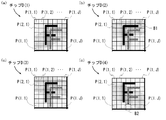
- FIG. 9 is an image diagram showing a divided region P (i, j) that is subdivided into a matrix with respect to the pattern of the chip Dz (n) picked up at the nth time.
- n 1 to N
- i 1 to I
- j 1 to J (the same applies hereinafter).
- the first chip Dz (1) to the fourth chip Dz (4) schematically represent circuit patterns using patterns in which two figures such as “F” having different line densities are overlapped.
- Each of the chips Dz (1) to Dz (4) is subdivided into a matrix of I rows ⁇ J columns, and respective divided regions P (1, 1) to P (I, J) are set.
- the luminance information Bz (1, i, j) of each divided region P (i, j) is acquired.
- the acquired luminance information B (1, i, j) is determined to be good or bad based on an allowable range associated with the luminance information B0 (i, j) of the chip D0 serving as a determination reference pattern.
- the chip Dz (1) is a non-defective product if the luminance information B (1, 1, 1) to B (1, i, j) of each divided region P is within the allowable range associated with the luminance information B0. Is determined.
- the chip Dz (2) shown in FIG. 9B includes the defective pattern B1
- the luminance information B of the divided area P of the portion is out of the allowable range associated with the luminance information B0 of the chip D0. It is determined as a defective product.
- the chip Dz (3) shown in FIG. 9C does not include a defective pattern, and the luminance information B of the divided area P in the portion is within the allowable range associated with the luminance information B0 of the chip D0. It is determined as a non-defective product.
- the chip Dz (4) shown in FIG. 9D includes the defective pattern B2, the luminance information B of the divided area P of the portion is out of the allowable range associated with the luminance information B0 of the chip D0. It is determined as a defective product.
- the chip D0 serving as a determination reference pattern in order to define the chip D0 serving as a determination reference pattern as a non-defective model, a plurality of non-defective products are selected from images acquired in the past, and the positions of the selected images are determined.
- the luminance information B of the corresponding divided area P is registered by averaging (for example, Patent Document 1).
- the surrounding pattern is also acquired at the same time, the average data of the eight images around the inspection target pattern is set as a non-defective model, and compared with the central inspection target pattern.
- the technique which performs is proposed (for example, patent document 2).
- the pattern formed on the substrate to be inspected is formed through a film forming process and a patterning process.
- the luminance information at the time of pattern inspection varies due to the influence of the film thickness change in the film forming process.
- the influence of the change of the film thickness in the spin coating for applying the photoresist is large, and the film thickness gradually changes from the center of the substrate to the peripheral part. Therefore, in the pattern inspection after exposure / development, the luminance information of the inspection target pattern gradually changes from the center of the substrate to the peripheral portion.
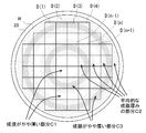
- FIG. 10 is a plan view of another semiconductor wafer on which a plurality of patterns to be inspected are arranged.
- the semiconductor wafer W is affected by a change in film thickness in the film forming process. For this reason, the semiconductor wafer W is gradually thinned from the center in the outer peripheral direction, and the film thickness gradually changes, and the part C1 with a slightly thin film, the part C2 with an average film thickness, and the part C3 with a slightly thick film However, it occurs several times concentrically.
- the semiconductor wafer W including such a change in film thickness
- the form in which a non-defective product model is specified from images acquired in the past and a determination reference pattern for determining pass / fail is specified
- the brightness of the acquired image it is possible to make an erroneous determination that a good product is a defective product.
- an erroneous determination that a defective product is a good product may be made.
- the present invention provides an appearance inspection apparatus and an appearance inspection method capable of performing strict pass / fail judgment without being affected by unevenness of film formation while maintaining good inspection resolution and a short inspection tact.
- an appearance inspection apparatus that images and inspects the appearance of the pattern on a substrate on which a plurality of patterns are repeatedly patterned
- a mounting table for mounting the substrate;
- a moving stage unit for moving the mounting table in a predetermined direction;
- An illumination unit that emits light toward the substrate;
- An imaging unit for imaging a pattern on the substrate;
- An image acquisition unit that acquires, as image data, a pattern on the substrate imaged by the imaging unit;
- an inspection pattern specifying unit that specifies at least a part of the region as an inspection target pattern image;
- About the inspection target pattern image a luminance information acquisition unit that acquires luminance information for each divided region divided into a matrix,
- a determination reference pattern registration unit for registering the previously acquired inspection target pattern as a determination reference pattern;
- a luminance difference calculation unit that compares the determination reference pattern with an inspection target pattern to be acquired next and is a target of pass / fail determination, and calculates a difference in luminance information for each of the divided
- the reference value for the pass / fail judgment is: A standard deviation set for each of the divided areas; Multiplying the standard deviation by a multiplication factor; An offset value that is added to a value obtained by multiplying the standard deviation by the magnification factor,
- the appearance inspection apparatus according to claim 1, further comprising a determination reference parameter registration unit that registers the offset value, the magnification count, and a standard deviation set for each divided region.
- the invention according to claim 3
- the determination reference pattern as a first inspection target pattern
- the second inspection target pattern is the inspection target pattern that is acquired next and is the target of pass / fail judgment, Obtaining a third inspection target circuit pattern different from the two inspection target patterns;
- a first luminance difference calculation unit for calculating a difference in luminance information between the first and second inspection target patterns;
- a second luminance difference calculation unit for calculating a difference in luminance information between the first and third inspection target patterns;
- In the pass / fail judgment section A first pass / fail determination unit that performs pass / fail determination on a difference in brightness information for each of the divided areas calculated by the first brightness difference calculation unit;
- a second pass / fail determination unit that performs pass / fail determination on the difference in brightness information for each of the divided areas calculated by the second brightness difference calculation unit; If one of the result of the first pass / fail determination unit and the result of the second pass / fail determination unit is a pass determination, the part is determined to be a passable product,
- the invention according to claim 4 4.
- the invention described in claim 5 The inspection target pattern is replaced with the determination reference pattern if the inspection target pattern to be inspected is determined to be a non-defective product in the quality determination unit. It is an appearance inspection device.
- the invention described in claim 6 Acquire the first to third inspection target patterns immediately after the start of inspection,
- the difference between the luminance information of the first and second inspection target patterns is the first difference
- the difference between the luminance information of the first and third inspection target patterns is the second difference
- In the pass / fail judgment unit A pass / fail determination is made for each of the first difference and the second difference, Determined by the pass / fail determination unit,
- the first inspection target pattern is registered as a non-defective product in the determination reference pattern registration unit if any one of the first difference and the second difference is determined to be good. 6.
- An appearance inspection apparatus according to any one of 1 to 5.
- a substrate mounting step for mounting the substrate on a mounting table;
- a table moving step for moving the mounting table in a predetermined direction;
- An illumination light irradiation step for irradiating light toward the substrate;
- An image acquisition step of acquiring the pattern on the substrate imaged in the imaging step as image data;
- An inspection pattern specifying step of specifying at least a part of the image data acquired in the image acquisition step as an inspection target pattern image;
- For the inspection target pattern image a luminance information acquisition step for acquiring luminance information for each divided region divided in a matrix,
- a determination reference pattern registration step for registering the previously acquired inspection target pattern as a determination reference pattern,
- a luminance difference calculation step of comparing the determination reference pattern with an inspection target pattern to be acquired next and being a pass / fail determination target, and calculating a difference in luminance information for each of the divided regions
- the invention according to claim 8 provides:
- the reference value for the pass / fail judgment is: A standard deviation set for each of the divided areas; Multiplying the standard deviation by a multiplication factor; An offset value that is added to a value obtained by multiplying the standard deviation by the magnification factor, 8.
- the invention according to claim 9 is: The determination reference pattern as a first inspection target pattern, Next, the second inspection target pattern is the inspection target pattern that is acquired next and is the target of pass / fail judgment, Obtaining a third test target circuit pattern different from the two different test target patterns;
- a first luminance difference calculating step for calculating a difference in luminance information between the first and second inspection target patterns;
- a second luminance difference calculating step for calculating a difference between luminance information of the first and third inspection target patterns;
- a first pass / fail judgment step for performing pass / fail judgment on the difference of the brightness information for each of the divided areas calculated in the first brightness difference calculating step;
- a second pass / fail determination step for determining pass / fail with respect to the difference in brightness information for each of the divided areas calculated in the second brightness difference calculating step; If any one of the result of the first pass / fail determination step and the result of the second pass / fail determination step is a pass determination, the portion is determined to be a
- the invention according to claim 10 is: 10.
- the invention according to claim 11 11.
- the inspection target pattern is replaced with the determination reference pattern if the inspection target pattern to be inspected is determined to be non-defective in the pass / fail determination step. This is an appearance inspection method.
- the invention according to claim 12 Acquire the first to third inspection target patterns immediately after the start of inspection,
- the difference between the luminance information of the first and second inspection target patterns is the first difference
- the difference between the luminance information of the first and third inspection target patterns is the second difference
- a pass / fail determination is made for each of the first difference and the second difference, Determined in the pass / fail determination step
- the registration of the determination reference pattern registration step is performed when one of the first difference and the second difference is determined to be good, and the first inspection target pattern is determined as non-defective.
- the visual inspection method according to any one of 7 to 11.
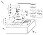
- the conceptual diagram which shows an example of the form which embodies this invention The conceptual diagram which shows the mode of the imaging in an example of the form which embodies this invention
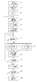
- the image acquisition flowchart in an example of the form which embodies the present invention The quality determination flowchart in an example of the embodiment embodying the present invention
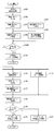
- the quality determination flowchart in another example of the embodiment embodying the present invention The quality determination flowchart in yet another example of the embodiment embodying the present invention
- FIG. 1 is a conceptual diagram showing an example of a form for embodying the present invention, in which a perspective view of an apparatus used for acquiring an image and a block diagram of a configuration necessary for an appearance inspection by acquiring an image are combined.
- the three axes of the orthogonal coordinate system are X, Y, and Z
- the XY plane is the horizontal plane
- the Z direction is the vertical direction.
- the direction of the arrow is represented as the top
- the opposite direction is represented as the bottom.
- the appearance inspection apparatus 1 includes a placement table 20, a moving stage unit 2, an illumination unit 3, an imaging unit 4, an image acquisition unit 5, an inspection pattern specifying unit 6, and a luminance information acquisition unit 7. And a determination reference pattern registration unit 8, a luminance difference calculation unit 9, a quality reference registration unit 10, and a quality determination unit 11.
- the mounting table 20 is for mounting the substrate W to be inspected, and has a flat surface in the XY direction.
- the mounting table 20 has grooves and pores formed in a portion where a substrate to be inspected is mounted. Further, the grooves and pores are connected to a vacuum source and a compressed air source via an open / close valve.
- the moving stage unit 2 moves the mounting table 20 to an arbitrary position on the XY plane.
- the moving stage unit 2 includes an X-axis slider 21 and a Y-axis slider 22.
- the X-axis slider 21 is mounted on the apparatus frame 1F, moves at a predetermined speed in the X direction, and can be stopped at an arbitrary position.
- the Y-axis slider 22 is mounted on the X-axis slider 21, moves at a predetermined speed in the Y direction, and can be stopped at an arbitrary position.
- the mounting table 20 is mounted on the Y-axis slider 22. Therefore, the moving stage unit 2 can move the mounting table 20 at a predetermined speed alone or in conjunction with each other in the X direction and the Y direction, and can stand still at an arbitrary position.
- the illumination unit 3 irradiates light toward the substrate W to be inspected, and includes a light source unit 31.
- the light source unit 31 is attached to the lens barrel 40, and the light 32 emitted from the light source unit 31 is reflected by the half mirror 41 incorporated in the lens barrel 40, passes through the objective lens 44a, and irradiates the substrate W. Is done.
- the light source unit 31 can be exemplified by using strobe illumination as a specific example.
- the strobe illumination is configured to repeat light emission at predetermined feed pitches in cooperation with the movement of the X-axis slider 21 and the Y-axis slider 22 of the moving stage unit 2.
- the light source part 31 is not restricted to the form directly attached to the lens-barrel 40, The thing of the form light-guided using a light guide from the light source installed in another place may be sufficient.
- the imaging unit 4 images a pattern on the substrate W to be inspected, and includes a lens barrel 40, a half mirror 41, an objective lens 44a, and an imaging camera 45.
- the imaging camera 45 is configured to include a light receiving element 46, and among the light 35 irradiated to the substrate W, the light 42 reflected by the observation region V on the substrate W is an objective lens 42 a, a half mirror 41, An image that passes through the lens barrel 43 and is irradiated on the light receiving element 46 is output to the outside as image data.
- imaging is performed simultaneously with the light emission of the strobe illumination, and image data is output. At this time, since the light emission time of the strobe illumination is very short, even an image captured during movement is captured in a state like a still image.
- the image acquisition unit 5 acquires a pattern included in the observation region V on the substrate W imaged by the light receiving element 46 of the imaging camera 45 as image data.
- the image acquisition unit 5 can be configured using a device called a so-called image processing apparatus.
- the image processing apparatus include a unit type having an image processing function and a type using a board called an image processing board incorporated in a personal computer or a workstation.
- the appearance inspection apparatus 1 Since the appearance inspection apparatus 1 according to the present invention is configured as described above, continuous imaging is performed while moving the mounting table 20 on which the substrate W to be inspected is placed at a predetermined speed, and the inspection object is inspected. Image data corresponding to the pattern can be acquired. Further, the acquired image data is judged as good or bad as described later.
- the position of the pattern (chip D) patterned on the actual substrate W varies, and the moving speed of the moving stage unit 2 varies. To do. Therefore, even if the same part is intended to be imaged every time, it may be acquired in a slightly shifted state. Therefore, the range of the observation region V imaged by the imaging unit 5 is set to be slightly wider than the range in which the pattern (chip D) necessary for actual inspection can be observed.
- FIG. 2 is a conceptual diagram showing a state of imaging in an example of a form embodying the present invention.
- a state in which chips D (4) are sequentially imaged is shown.
- the imaging camera 45 is imaging the third chip D (3).
- the range of the observation region V set slightly wider than the chip D (3) is projected onto the light receiving element 46.
- the inspection pattern specifying unit 6 specifies at least a part of the image data acquired by the image acquisition unit 5 as an inspection target pattern image.
- the inspection pattern specifying unit 6 is configured by using a device called an image processing apparatus similar to the image acquiring unit 5, and specifying necessary for appearance inspection from the image data acquired by the image acquiring unit 5.
- the inspection pattern is extracted. If it demonstrates using FIG. 2, the area
- the processing to be specified is performed based on the alignment position of the periphery of each chip D (n), the peripheral pattern, and the relative position of the internal pattern, and the corresponding positions of the patterns to be compared in the processing described later are Make sure they are aligned.
- the entire region of the observation region V and each chip D (n) are identified by extracting a necessary pattern, for example, by trimming unnecessary peripheral portions of the acquired image data, It can be used for comparison processing and luminance difference processing described later.
- the luminance information acquisition unit 7 finely divides the image specified as the inspection target pattern image into a matrix, and acquires luminance information for each divided area P.
- Each of the divided areas P is, for example, a minute area corresponding to each of the light receiving elements 46 of the imaging camera 45, or a group of several light receiving elements (100 ⁇ 100 or 1000 ⁇ 1000) or the like.
- FIG. 3 is a conceptual diagram showing divided areas of an acquired image in an example of a form embodying the present invention.
- the first chip D (1) to the fourth chip D (4) on the substrate W which is the specified pattern image to be inspected, are divided into a matrix-like divided region P of I rows ⁇ J columns.
- luminance information about P (i, j) for each divided area of the nth chip D (n) is expressed as luminance information B (n, i, j).
- the luminance information B (n, i, j) is determined by an output signal from the imaging camera 45 and is expressed by, for example, a value by an 8-bit signal (tone data from black: 0 to white: 255).
- the determination reference pattern registration unit A registers the previously acquired inspection target pattern as a determination reference pattern. Specifically, the first inspection target pattern of the substrate to be inspected is set, the pattern inspected immediately before in the flow of sequential inspection, or the flow of sequential inspection Among them, the pattern determined to be non-defective is set last (in other words, immediately before). For example, the luminance information B (n ⁇ 1, i, j) of the “n ⁇ 1” th chip D (n ⁇ 1) immediately before the nth chip D (n) is stored in the determination reference pattern registration unit A. Register.
- the luminance difference calculation unit 8 compares a determination reference pattern with an inspection target pattern that is acquired next and is a target of pass / fail determination, and calculates a difference in luminance information for each divided region corresponding to each position. is there. Specifically, the luminance information B (n, i, j) of the nth chip D (n) and the luminance of the “n ⁇ 1” th chip D (n ⁇ 1) registered as the determination reference pattern. A difference def (n, i, j) from the information B (n-1, i, j) is calculated using the following equation.
- the pass / fail criterion registration unit B registers in advance a pass / fail judgment reference value for the difference in brightness information for each divided coordinate calculated by the brightness difference calculation unit for each divided region. Specifically, when the luminance information B is acquired as a value by an 8-bit signal (tone data from black: 0 to white: 255), the reference value for pass / fail judgment is ⁇ 5 in a certain range of divided areas.
- the reference values for pass / fail judgment are set individually such that the reference value for pass / fail judgment is ⁇ 10 in the divided areas of another range, and the reference value for pass / fail judgment is ⁇ 20 in the divided areas of another range.
- Table 1 shows an example of the pass / fail criterion table for the chip D (n) of the type K.
- a criterion def0 (i, j) is defined for each divided region P (i, j).
- the criterion def0 (i, j) corresponding to P (i, j) is defined as “20”, “10”, “5”, the luminance difference of the divided region P (i, j) is If it is “within ⁇ 20”, “within ⁇ 10”, or “within ⁇ 5”, it means that it can be determined as a non-defective product.
- the data table of this determination criterion def0 (i, j) is registered in advance in association with the product information of the chip D.
- the determination reference data table may be in the form exemplified above, but it is more preferable to do the following.
- the criterion def0 (i, j) which is a criterion value for pass / fail judgment, is not a fixed value but a value represented by Equation (2).
- the standard deviation ⁇ (i, j) set for each divided region P (i, j) is calculated from the distribution of luminance information of the pattern image to be inspected acquired from a plurality of chips that are known to be non-defective in advance.
- the intermediate value between b1 and b2 is set as the sensitivity.
- the above-determined a and b are inspected, and if over-detection does not occur, this value is adopted, and if over-detection occurs, the value of a is increased to 1) to 3) above. To implement.
- Each criterion parameter thus set: standard deviation ⁇ (i, j), magnification factor b, offset value a set for each divided region P (i, j), and formula for calculating the criterion value
- pass / fail determination is performed. In this pass / fail judgment, if def (i, j) is within a range of ⁇ ⁇ a + b ⁇ ⁇ (i, j) ⁇ , that is, if Formula (3) is satisfied, it is judged as a non-defective product.
- the criterion def0 (i, j) is not a fixed value, Standard deviation ⁇ (i, j) for each divided region derived from a plurality of non-defective samples, It can be quickly set using two parameters a and b determined by the person in charge of inspection. By doing so, it is possible to perform inspection within a wide allowable range for a portion with originally large variation, and to perform inspection with a narrow allowable range for a portion with originally small variation.
- the pass / fail judgment unit 9 performs pass / fail judgment for each divided region of the inspection target pattern based on the pass / fail judgment reference value. Specifically, when the reference value for pass / fail judgment is set to “5” in a certain area, the difference in luminance information of the corresponding divided areas between the previous image data and the subsequent image data is “ If it is “within ⁇ 5”, the product is judged as non-defective, otherwise it is judged as defective. Alternatively, as described above, the quality determination is performed as a non-defective product if Equation (3) is satisfied, and as a defective product if it is not considered.
- the appearance inspection apparatus 1 Since the appearance inspection apparatus 1 according to the present invention has the above-described configuration, it is possible to perform pass / fail determination from the difference between the image data acquired first and the image data acquired later.
- the result of the pass / fail judgment is displayed on an information display provided in the appearance inspection apparatus 1, stored in a data collection unit, or transmitted to a host computer connected to the appearance inspection apparatus 1 through a communication line.
- the information display is configured using a so-called display monitor such as a liquid crystal display.
- the data collection unit is configured using an information recording medium such as a memory or a hard disk.
- FIG. 4 is an image acquisition flowchart in an example of a form embodying the present invention.
- FIG. 4 shows a series of steps for acquiring image data of each inspection target pattern for each step in order to inspect a plurality of inspection target patterns arranged on the substrate W.
- the substrate W to be inspected is placed on the placement table 20 of the appearance inspection apparatus 1 (s1: substrate placement step).
- pre-registered inspection conditions and the like are read (s2), moved to a reference mark reading position formed on the substrate W, and an alignment operation is performed (s3).
- the mounting table 20 is moved to the movement start position in the first row (s4), the moving stage unit 2 is moved at a predetermined speed, and the movement of the mounting table 20 is started (s5: table moving step). .
- the current position information of the mounting table 20 is acquired from the X-axis position detector and the Y-axis position detector of the moving stage unit 2 (s6).
- the imaging camera 45 Based on the acquired current position information of the mounting table 20, it is determined whether or not it is a position where the imaging camera 45 should image the substrate W (s 7). If the current position of the mounting table 20 is a position where the imaging camera 45 should image the substrate W, strobe illumination is emitted toward the substrate W (s8: illumination light irradiation step), and at the same time, it is reflected from the substrate W. The captured light is imaged by the imaging camera 45 (s9: imaging step).
- the image data captured by the imaging camera 45 will be described in detail later, but an image is acquired and a pass / fail judgment is made (s10).
- step s21 While continuing the movement of the mounting table 20, it is determined based on the current position information whether or not one line of imaging has been completed (s21). If it is determined that the imaging of the first row has been completed, the movement of the moving stage unit 2 is stopped (s22). On the other hand, if it is determined in step s21 that the imaging in the first row has not been completed, steps s8 to s21 are repeated.
- step s22 it is determined whether or not the imaging of all the columns is completed on the substrate W (s23). If it is determined that all the imaging is completed, the substrate W is taken out from the mounting table 20 (s24). . On the other hand, if it is determined in step s23 that the imaging of all the rows has not been completed, the placement table 20 is moved to the measurement start position of the next row (s4), and the steps necessary for the series of image acquisition ( Repeat s4 to s23).
- FIG. 5 is a pass / fail judgment flowchart in an example of a form embodying the present invention.
- a series of steps for continuously determining pass / fail based on the image data acquired in step s10 is shown in detail for each step.
- the pattern on the substrate W imaged in the imaging step (s9) is acquired as image data (s105: image acquisition step).
- image data is acquired as image data (s105: image acquisition step).
- inspection target pattern image is specified as an inspection target pattern image (s106: inspection pattern specifying step).
- a so-called trimming process also referred to as a crop process
- processing for extracting and specifying the inspection target pattern included in the image data is performed based on positioning reference marks arranged in and around the inspection target pattern.
- the inspection target pattern image identified in step s106 is divided into a matrix and luminance information is acquired for each divided region (s107: luminance information acquisition step).
- the nth chip D (n) on the substrate W is subdivided into I-row ⁇ J-column matrix-like divided areas to define individual divided areas P (i, j).
- the luminance information B (n, i, j) is acquired for each divided region P (i, j).
- the acquired luminance information B (n, i, j) is stored in a temporary storage memory in the image processing unit or stored in a data recording medium connected to the image processing unit.
- the inspection target pattern that is, the (n ⁇ 1) -th chip D (n ⁇ 1) acquired immediately before the inspection target pattern is used as the determination reference pattern.
- S10A determination reference pattern registration step
- the luminance information B (n, i, j) of the nth chip D (n) and the luminance information B (n ⁇ 1) of the “n ⁇ 1” th chip D (n ⁇ 1) as the determination reference pattern. , I, j) is calculated (s108: luminance difference calculation step).
- the pass / fail judgment standard def0 (n, i, j), which is the pass / fail judgment standard, is registered in advance (s10B: pass / fail standard registration step).
- step s108 the luminance difference def (n, i, j) calculated in step s108 is compared with a pass / fail judgment criterion def0 (n, i, j), and each divided region P (i, j) of the nth chip D (n) is compared. J) is judged for pass / fail (s109: pass / fail judgment step).
- the luminance information B (n, i, j) of the nth chip D (n) is updated and registered as a determination reference pattern used for the next (n + 1) th inspection (s110).
- the determination for registering the offset value, the magnification factor, and the standard deviation set for each divided region is performed in the same manner as in the aspect related to the appearance inspection apparatus described above.
- the method further includes a reference parameter registration step. By doing so, it is possible to perform a strict quality determination without being affected by film formation unevenness. In addition, it is not necessary to manually set the pass / fail judgment reference value for each divided area, so that it can be quickly reset and operated.
- the subsequent inspection target pattern is determined as a defective product.
- the determination reference pattern is set as the first inspection target pattern
- the inspection target pattern to be acquired and passed next is set as the second inspection target pattern, and is different from these two inspection target patterns.
- a third circuit pattern to be inspected is acquired. Then, the following two-step determination is performed so that the pass / fail determination can be performed correctly.
- the appearance inspection apparatus 1B has the same apparatus configuration as the appearance inspection apparatus 1 described above, includes a first luminance difference calculation unit 7A and a second luminance difference calculation unit 7B, and replaces the pass / fail determination unit 9.
- the pass / fail judgment unit 9B is included.
- the first luminance difference calculation unit 7A has the same configuration as the luminance difference calculation unit 7 of the appearance inspection apparatus 1, but when inspecting the nth chip D (n), the n ⁇ 1th as described above.
- the difference def (n, i, j) of luminance information is calculated in comparison with the chip D (n ⁇ 1).
- the second luminance difference calculation unit 7B has the same configuration as the luminance difference calculation unit 7 of the appearance inspection apparatus 1, but when inspecting the nth chip D (n), the second luminance difference calculation unit 7B
- the difference def (n + 1, i, j) of the luminance information is calculated by comparing with the (n + 1) th chip D (n + 1).
- the pass / fail determination unit 9B further includes a first pass / fail determination unit 9A, a second pass / fail determination unit 9B, and an overall determination unit 5C.
- the first pass / fail judgment unit 9A compares the brightness information difference def (n, i, j) with the pass / fail judgment criterion def0 (n, i, j) to make a pass / fail judgment, and the first pass / fail result is determined. Output as judgment result.
- the second pass / fail judgment unit 9B compares the brightness information difference def (n + 1, i, j) with the pass / fail judgment criterion def0 (n, i, j) to make a pass / fail judgment, and the result of the pass / fail judgment is the second pass / fail. Output as judgment result.
- the overall determination unit 9C determines that the part is “non-defective” if either the result of the first pass / fail determination unit or the result of the second pass / fail determination unit is “good”. If both the result of the first pass / fail determination unit and the result of the second pass / fail determination unit are “defective” determination, the part is determined to be “defective”.
- the appearance inspection apparatus 1B When inspecting the nth chip D (n), the appearance inspection apparatus 1B according to the present invention not only compares with the image of the n ⁇ 1th chip D (n ⁇ 1) as described above, but also adds n + 1. The determination is made in consideration of the comparison result with the image of the second chip D (n + 1).
- FIG. 6 is a pass / fail judgment flow chart in another example of a form embodying the present invention.
- FIG. 6 shows a pass / fail judgment flow for the appearance inspection method corresponding to the appearance inspection apparatus 1B according to the present invention.
- Steps s105 to s108 are the same as the appearance inspection method corresponding to the appearance inspection apparatus 1 shown in FIG.
- step s109B first pass / fail judgment step. If it is a defective product, the judgment reference pattern is updated (s110), and the next (n + 1) th image is displayed. Obtaining (s125), specifying the inspection pattern (s126), obtaining the luminance information B (n + 1, i, j) (s127), and calculating the luminance difference def (n + 1, i, j) (s128).
- a pass / fail judgment is performed on the luminance difference def (n + 1, i, j) (s129: second pass / fail judgment step). If def (n + 1, i, j) is within the judgment criteria, the nth chip D ( n) is determined as non-defective (s131). On the other hand, if def (n + 1, i, j) is not within the criterion, the nth chip D (n) is determined as a defective product (s132).
- the chip D (n-1) is a good product
- D (n) is a defective product
- D (n + 1) is a good product. Even if the inspection target pattern is acquired, it is possible to correctly determine the quality of each.
- the acquired inspection target pattern is preferably a pattern arranged at an adjacent position. If it does so, image data can be acquired at a fixed interval by making the illumination strobe light at a predetermined interval while moving the mounting table at a predetermined speed. By adjusting this interval to the processing tact of the appearance inspection apparatuses 1 and 1B, the inspection can be performed with the shortest processing tact.
- the inspection target pattern determined as a non-defective product at the end is registered as a determination reference pattern. Specifically, when it is determined as “defective”, the pattern is not updated as the determination reference pattern, and the inspection target pattern determined as “non-defective” immediately before is maintained as the determination reference pattern. By doing so, even if defective products are continuously present, the defective product can be correctly determined as “defective” as compared with the determination reference pattern registered in advance as non-defective products.
- FIG. 7 is a pass / fail judgment flow chart in still another example of the embodiment embodying the present invention, and shows a specific procedure for first judging whether or not the first chip of the substrate to be inspected is a non-defective product. ing.
- the first to third inspection target patterns immediately after the start of inspection are acquired. Then, in the luminance difference calculation unit, The difference between the luminance information of the first and second inspection target patterns is the first difference, The difference between the luminance information of the first and third inspection target patterns is calculated as the second difference.
- An image of the first chip D (1) immediately after the start of inspection is acquired (s305), and then an image of the second chip D (2) is acquired (s315), and the third chip D ( The image of 3) is acquired (s325).
- the inspection pattern is specified (s306), and the luminance information B (1) is acquired (s307).
- the inspection pattern is specified (s316), and the luminance information B (2) is acquired (s317).
- the inspection pattern is specified (s326), and the luminance information B (3) is acquired (s327).
- the luminance difference between the inspection target patterns of the first chip D (1) and the second chip D (2) is calculated as the first difference def (1-2) (s318). Further, the luminance difference between the inspection target patterns of the first chip D (1) and the third chip D (3) is calculated as the second difference def (1-3) (s328).
- the pass / fail determination is performed on the first difference def (f1-2) and the second difference def (1-3), and if any of the pass / fail determination results of the first difference and the second difference is a pass / fail determination,
- the first inspection target pattern is registered as a non-defective product in the determination reference pattern registration unit.
- a pass / fail determination is made for the first difference def (1-2) (s319), and if it is determined as “defective product”, a pass / fail determination is made for the second difference def (1-3) (s329). If any of step s319 and step 329 is determined as “non-defective”, the chip D (1) as the first inspection target pattern is determined as non-defective (s331) and registered in the determination reference pattern registration unit. To do.
- step s319 and step 329 are determined as “defective products”, the chip D (1) as the first pattern is determined as a defective product (s332).
- the chip D (1) as the first pattern is determined as a defective product (s332).
- an image of the fourth chip D (4) is subsequently acquired, and the same processing as described above is performed, and the second and third inspection patterns, and the second and fourth inspection patterns are obtained. Comparison is made, each difference is calculated, and pass / fail judgment is performed. By doing so, appearance inspection can be started without preparing a good product model as in the prior art.
- the first inspection pattern in addition to obtaining the first to third inspection patterns, further obtaining a fourth pattern, the first inspection pattern and the first An appearance inspection apparatus and method in which the quality is determined based on the difference in luminance information of the second to fourth inspection patterns may be used. Then, there is non-regular film formation unevenness in the peripheral portion of the substrate to be inspected, and it is not possible to determine whether the first pattern is a non-defective product by simply comparing the first to third inspection patterns. Even in a case where it is determined as “defective product”, it is more preferable that the non-defective product can be correctly determined as “defective product” by adding the fourth pattern.
- the imaging camera 45 a camera in which a 1-inch size light receiving element 46 having 2352 ⁇ 1728 effective vertical and horizontal effective pixels is incorporated is used.
- a xenon flash lamp having a rated output of 40 W and a half width of about 1 usec is used. Since a plurality of objective lenses can be attached, an appropriate objective lens is selected according to the defect to be detected.
- the objective lens 44 has a magnification of 1 ⁇ Observation field of view: length: 16.46 mm ⁇ width: 12.1 mm Pixel size is 7 ⁇ m
- the objective lens 44 has a magnification of 10 times.
- Observation field of view: length: 1.65 mm ⁇ width: 1.21 mm Pixel size is 0.7 ⁇ m It becomes.
Landscapes
- Physics & Mathematics (AREA)
- Health & Medical Sciences (AREA)
- Life Sciences & Earth Sciences (AREA)
- Chemical & Material Sciences (AREA)
- Analytical Chemistry (AREA)
- Biochemistry (AREA)
- General Health & Medical Sciences (AREA)
- General Physics & Mathematics (AREA)
- Immunology (AREA)
- Pathology (AREA)
- Investigating Materials By The Use Of Optical Means Adapted For Particular Applications (AREA)
Applications Claiming Priority (2)
| Application Number | Priority Date | Filing Date | Title |
|---|---|---|---|
| JP2012126912A JP2013250225A (ja) | 2012-06-04 | 2012-06-04 | 外観検査装置及び外観検査方法 |
| JP2012-126912 | 2012-06-04 |
Publications (1)
| Publication Number | Publication Date |
|---|---|
| WO2013183471A1 true WO2013183471A1 (fr) | 2013-12-12 |
Family
ID=49711864
Family Applications (1)
| Application Number | Title | Priority Date | Filing Date |
|---|---|---|---|
| PCT/JP2013/064574 Ceased WO2013183471A1 (fr) | 2012-06-04 | 2013-05-27 | Dispositif d'inspection d'apparence et procédé d'inspection d'apparence |
Country Status (3)
| Country | Link |
|---|---|
| JP (1) | JP2013250225A (fr) |
| TW (1) | TW201405120A (fr) |
| WO (1) | WO2013183471A1 (fr) |
Families Citing this family (8)
| Publication number | Priority date | Publication date | Assignee | Title |
|---|---|---|---|---|
| JP6012655B2 (ja) * | 2014-03-28 | 2016-10-25 | 東レエンジニアリング株式会社 | ウエーハ検査装置の検査条件データ生成方法及び検査条件データ生成システム |
| JP6351408B2 (ja) * | 2014-07-08 | 2018-07-04 | アズビル株式会社 | 画像検査装置および画像検査方法 |
| JP6936577B2 (ja) * | 2017-01-20 | 2021-09-15 | 株式会社Screenホールディングス | 位置ずれ量取得装置、検査装置、位置ずれ量取得方法および検査方法 |
| JP7048979B2 (ja) * | 2019-07-24 | 2022-04-06 | 株式会社ホニック | 段成形検査方法 |
| JP7353717B2 (ja) * | 2019-11-22 | 2023-10-02 | 株式会社指月電機製作所 | 金属化フィルムの検査方法及び検査装置 |
| CN111239152B (zh) * | 2020-01-02 | 2023-11-17 | 长江存储科技有限责任公司 | 晶圆检测方法、装置和设备 |
| JP7714414B2 (ja) * | 2021-09-13 | 2025-07-29 | ファスフォードテクノロジ株式会社 | ダイボンディング装置および半導体装置の製造方法 |
| CN116835407A (zh) * | 2023-06-16 | 2023-10-03 | 广东寰宇电子科技股份有限公司 | 一种用于导轨对接的视觉检测方法及装置 |
Citations (10)
| Publication number | Priority date | Publication date | Assignee | Title |
|---|---|---|---|---|
| JPS61205811A (ja) * | 1985-03-11 | 1986-09-12 | Hitachi Ltd | 欠陥検出方法 |
| JPH05281151A (ja) * | 1992-04-02 | 1993-10-29 | Nippondenso Co Ltd | ウエハパターン検査装置 |
| JPH0618428A (ja) * | 1992-07-01 | 1994-01-25 | Seiko Epson Corp | 欠陥検査方法及び半導体装置の製造方法 |
| JPH0727708A (ja) * | 1993-07-09 | 1995-01-31 | Sony Corp | ウエハの欠陥検査方法 |
| JP2000105203A (ja) * | 1998-07-28 | 2000-04-11 | Hitachi Ltd | 欠陥検査装置およびその方法 |
| JP2000131240A (ja) * | 1998-10-28 | 2000-05-12 | Tokyo Seimitsu Co Ltd | パターン比較方法および外観検査装置 |
| JP2007149837A (ja) * | 2005-11-25 | 2007-06-14 | Tokyo Seimitsu Co Ltd | 画像欠陥検査装置、画像欠陥検査システム及び画像欠陥検査方法 |
| JP2007192759A (ja) * | 2006-01-23 | 2007-08-02 | Hitachi High-Technologies Corp | 欠陥検査装置およびその方法 |
| JP2008058111A (ja) * | 2006-08-30 | 2008-03-13 | Hitachi High-Technologies Corp | 欠陥検査装置、及び欠陥検査方法 |
| JP2009002743A (ja) * | 2007-06-20 | 2009-01-08 | Hitachi High-Technologies Corp | 外観検査方法及びその装置および画像処理評価システム |
-
2012
- 2012-06-04 JP JP2012126912A patent/JP2013250225A/ja active Pending
-
2013
- 2013-05-27 WO PCT/JP2013/064574 patent/WO2013183471A1/fr not_active Ceased
- 2013-06-04 TW TW102119830A patent/TW201405120A/zh unknown
Patent Citations (10)
| Publication number | Priority date | Publication date | Assignee | Title |
|---|---|---|---|---|
| JPS61205811A (ja) * | 1985-03-11 | 1986-09-12 | Hitachi Ltd | 欠陥検出方法 |
| JPH05281151A (ja) * | 1992-04-02 | 1993-10-29 | Nippondenso Co Ltd | ウエハパターン検査装置 |
| JPH0618428A (ja) * | 1992-07-01 | 1994-01-25 | Seiko Epson Corp | 欠陥検査方法及び半導体装置の製造方法 |
| JPH0727708A (ja) * | 1993-07-09 | 1995-01-31 | Sony Corp | ウエハの欠陥検査方法 |
| JP2000105203A (ja) * | 1998-07-28 | 2000-04-11 | Hitachi Ltd | 欠陥検査装置およびその方法 |
| JP2000131240A (ja) * | 1998-10-28 | 2000-05-12 | Tokyo Seimitsu Co Ltd | パターン比較方法および外観検査装置 |
| JP2007149837A (ja) * | 2005-11-25 | 2007-06-14 | Tokyo Seimitsu Co Ltd | 画像欠陥検査装置、画像欠陥検査システム及び画像欠陥検査方法 |
| JP2007192759A (ja) * | 2006-01-23 | 2007-08-02 | Hitachi High-Technologies Corp | 欠陥検査装置およびその方法 |
| JP2008058111A (ja) * | 2006-08-30 | 2008-03-13 | Hitachi High-Technologies Corp | 欠陥検査装置、及び欠陥検査方法 |
| JP2009002743A (ja) * | 2007-06-20 | 2009-01-08 | Hitachi High-Technologies Corp | 外観検査方法及びその装置および画像処理評価システム |
Also Published As
| Publication number | Publication date |
|---|---|
| JP2013250225A (ja) | 2013-12-12 |
| TW201405120A (zh) | 2014-02-01 |
Similar Documents
| Publication | Publication Date | Title |
|---|---|---|
| JP2013250225A (ja) | 外観検査装置及び外観検査方法 | |
| KR101735403B1 (ko) | 검사 방법, 템플릿 기판 및 포커스 오프셋 방법 | |
| US6198529B1 (en) | Automated inspection system for metallic surfaces | |
| US6292260B1 (en) | System and method of optically inspecting surface structures on an object | |
| US7460219B2 (en) | Method for optically inspecting a wafer by sequentially illuminating with bright and dark field light beams wherein the images from the bright and dark field illuminated regions are spatially offset | |
| US20100302364A1 (en) | Three dimensional shape measurement apparatus and method | |
| TWI289719B (en) | Inspection system imager method for inspecting surfaces for defect and method for fabricating electrical circuit | |
| JP2016145887A (ja) | 検査装置および検査方法 | |
| KR20100067659A (ko) | 관찰 장치, 관찰 방법, 검사 장치 및 검사 방법 | |
| JP2011123019A (ja) | 画像検査装置 | |
| KR101146081B1 (ko) | 마이크로-검사 입력을 이용한 매크로 결함 검출 방법 및시스템 | |
| JP5178781B2 (ja) | センサ出力データの補正装置及びセンサ出力データの補正方法 | |
| KR101320183B1 (ko) | 패턴 결함 검사 방법, 패턴 결함 검사 장치, 포토마스크의 제조 방법, 및 표시 디바이스용 기판의 제조 방법 | |
| US20060158643A1 (en) | Method and system of inspecting mura-defect and method of fabricating photomask | |
| JP4111613B2 (ja) | 半導体検査方法及び装置 | |
| JP2000283929A (ja) | 配線パターン検査方法及びその装置 | |
| JP2007178144A (ja) | パターン検査装置、パターン検査方法、検査対象試料、及び検査対象試料の管理方法 | |
| KR102847060B1 (ko) | 얼라인먼트 장치 및 얼라인먼트 방법 | |
| JP2009075068A (ja) | パターン検査装置及びパターン検査方法 | |
| JP3944075B2 (ja) | 試料検査方法及び検査装置 | |
| JP2004212353A (ja) | 光学的検査装置 | |
| JP2006275780A (ja) | パターン検査方法 | |
| JPH0522176B2 (fr) | ||
| JP2008068284A (ja) | 欠陥修正装置、欠陥修正方法、及びパターン基板の製造方法 | |
| JP7362324B2 (ja) | 画像表示装置の検査方法、製造方法及び検査装置 |
Legal Events
| Date | Code | Title | Description |
|---|---|---|---|
| 121 | Ep: the epo has been informed by wipo that ep was designated in this application |
Ref document number: 13799935 Country of ref document: EP Kind code of ref document: A1 |
|
| NENP | Non-entry into the national phase |
Ref country code: DE |
|
| 122 | Ep: pct application non-entry in european phase |
Ref document number: 13799935 Country of ref document: EP Kind code of ref document: A1 |