WO2013187070A1 - 高純度多結晶シリコンの製造方法 - Google Patents
高純度多結晶シリコンの製造方法 Download PDFInfo
- Publication number
- WO2013187070A1 WO2013187070A1 PCT/JP2013/003729 JP2013003729W WO2013187070A1 WO 2013187070 A1 WO2013187070 A1 WO 2013187070A1 JP 2013003729 W JP2013003729 W JP 2013003729W WO 2013187070 A1 WO2013187070 A1 WO 2013187070A1
- Authority
- WO
- WIPO (PCT)
- Prior art keywords
- polycrystalline silicon
- carbon
- sim
- trichlorosilane
- column
- Prior art date
- Legal status (The legal status is an assumption and is not a legal conclusion. Google has not performed a legal analysis and makes no representation as to the accuracy of the status listed.)
- Ceased
Links
Images






Classifications
-
- C—CHEMISTRY; METALLURGY
- C01—INORGANIC CHEMISTRY
- C01B—NON-METALLIC ELEMENTS; COMPOUNDS THEREOF; METALLOIDS OR COMPOUNDS THEREOF NOT COVERED BY SUBCLASS C01C
- C01B33/00—Silicon; Compounds thereof
- C01B33/02—Silicon
- C01B33/021—Preparation
- C01B33/027—Preparation by decomposition or reduction of gaseous or vaporised silicon compounds other than silica or silica-containing material
- C01B33/03—Preparation by decomposition or reduction of gaseous or vaporised silicon compounds other than silica or silica-containing material by decomposition of silicon halides or halosilanes or reduction thereof with hydrogen as the only reducing agent
-
- C—CHEMISTRY; METALLURGY
- C01—INORGANIC CHEMISTRY
- C01B—NON-METALLIC ELEMENTS; COMPOUNDS THEREOF; METALLOIDS OR COMPOUNDS THEREOF NOT COVERED BY SUBCLASS C01C
- C01B33/00—Silicon; Compounds thereof
- C01B33/02—Silicon
- C01B33/021—Preparation
- C01B33/027—Preparation by decomposition or reduction of gaseous or vaporised silicon compounds other than silica or silica-containing material
- C01B33/035—Preparation by decomposition or reduction of gaseous or vaporised silicon compounds other than silica or silica-containing material by decomposition or reduction of gaseous or vaporised silicon compounds in the presence of heated filaments of silicon, carbon or a refractory metal, e.g. tantalum or tungsten, or in the presence of heated silicon rods on which the formed silicon is deposited, a silicon rod being obtained, e.g. Siemens process
-
- G—PHYSICS
- G01—MEASURING; TESTING
- G01N—INVESTIGATING OR ANALYSING MATERIALS BY DETERMINING THEIR CHEMICAL OR PHYSICAL PROPERTIES
- G01N33/00—Investigating or analysing materials by specific methods not covered by groups G01N1/00 - G01N31/00
-
- H—ELECTRICITY
- H10—SEMICONDUCTOR DEVICES; ELECTRIC SOLID-STATE DEVICES NOT OTHERWISE PROVIDED FOR
- H10P—GENERIC PROCESSES OR APPARATUS FOR THE MANUFACTURE OR TREATMENT OF DEVICES COVERED BY CLASS H10
- H10P14/00—Formation of materials, e.g. in the shape of layers or pillars
- H10P14/20—Formation of materials, e.g. in the shape of layers or pillars of semiconductor materials
- H10P14/24—Formation of materials, e.g. in the shape of layers or pillars of semiconductor materials using chemical vapour deposition [CVD]
-
- H—ELECTRICITY
- H10—SEMICONDUCTOR DEVICES; ELECTRIC SOLID-STATE DEVICES NOT OTHERWISE PROVIDED FOR
- H10P—GENERIC PROCESSES OR APPARATUS FOR THE MANUFACTURE OR TREATMENT OF DEVICES COVERED BY CLASS H10
- H10P14/00—Formation of materials, e.g. in the shape of layers or pillars
- H10P14/20—Formation of materials, e.g. in the shape of layers or pillars of semiconductor materials
- H10P14/34—Deposited materials, e.g. layers
- H10P14/3402—Deposited materials, e.g. layers characterised by the chemical composition
- H10P14/3404—Deposited materials, e.g. layers characterised by the chemical composition being Group IVA materials
- H10P14/3411—Silicon, silicon germanium or germanium
-
- H—ELECTRICITY
- H10—SEMICONDUCTOR DEVICES; ELECTRIC SOLID-STATE DEVICES NOT OTHERWISE PROVIDED FOR
- H10P—GENERIC PROCESSES OR APPARATUS FOR THE MANUFACTURE OR TREATMENT OF DEVICES COVERED BY CLASS H10
- H10P14/00—Formation of materials, e.g. in the shape of layers or pillars
- H10P14/20—Formation of materials, e.g. in the shape of layers or pillars of semiconductor materials
- H10P14/34—Deposited materials, e.g. layers
- H10P14/3451—Structure
- H10P14/3452—Microstructure
- H10P14/3456—Polycrystalline
-
- H—ELECTRICITY
- H10—SEMICONDUCTOR DEVICES; ELECTRIC SOLID-STATE DEVICES NOT OTHERWISE PROVIDED FOR
- H10P—GENERIC PROCESSES OR APPARATUS FOR THE MANUFACTURE OR TREATMENT OF DEVICES COVERED BY CLASS H10
- H10P74/00—Testing or measuring during manufacture or treatment of wafers, substrates or devices
- H10P74/20—Testing or measuring during manufacture or treatment of wafers, substrates or devices characterised by the properties tested or measured, e.g. structural or electrical properties
-
- C—CHEMISTRY; METALLURGY
- C01—INORGANIC CHEMISTRY
- C01P—INDEXING SCHEME RELATING TO STRUCTURAL AND PHYSICAL ASPECTS OF SOLID INORGANIC COMPOUNDS
- C01P2006/00—Physical properties of inorganic compounds
- C01P2006/80—Compositional purity
-
- G—PHYSICS
- G01—MEASURING; TESTING
- G01N—INVESTIGATING OR ANALYSING MATERIALS BY DETERMINING THEIR CHEMICAL OR PHYSICAL PROPERTIES
- G01N33/00—Investigating or analysing materials by specific methods not covered by groups G01N1/00 - G01N31/00
- G01N33/0095—Semiconductive materials
Definitions
- the present invention relates to a technology for producing high-purity polycrystalline silicon, and more particularly to a technology for realizing high-purity polycrystalline silicon by using a source gas having a low concentration of carbon-containing impurities.
- Semiconductor grade high-purity polycrystalline silicon is usually a CVD method called “Siemens method” using, as a raw material, a chlorosilane gas mainly composed of trichlorosilane in the presence of hydrogen (for example, Patent Document 1: Japanese Patent Laid-Open No. 56-73617). Manufactured by the official gazette).
- chlorosilanes for producing polycrystalline silicon are prepared by reacting metallurgical grade silicon with hydrogen chloride (see, for example, Patent Document 2: JP-A-2-208217 and Patent Document 3: JP-A-9-169514)
- Patent Document 4 JP-A-60-36318 and Patent Document 5: JP-A-10-29813.
- the synthesized chlorosilanes contain impurities derived from metallurgical grade silicon or the like used as a raw material, chemical treatment for increasing the purity (for example, Patent Document 6: JP 2009-62213 A). And after high-precision distillation, it is used as a raw material for producing polycrystalline silicon.
- Such purification ie, removal of impurities
- the reason for this is that when the contained impurities are phosphorus or arsenic serving as a donor in silicon crystal, or boron or aluminum serving as an acceptor, even if the content of these impurities is very small, polycrystalline silicon This is because when it is taken in, the electrical characteristics (resistivity) are significantly affected. Accordingly, donor impurities and acceptor impurities contained in the raw material chlorosilanes are removed by various methods (for example, chemical treatment as in Patent Document 6).
- Carbon impurities also form impurity levels in the band gap in silicon crystals to act as carrier traps, or accelerate the formation of oxygen precipitation nuclei in the crystal during the semiconductor device manufacturing process. Inducing crystal defects. For this reason, in semiconductor grade polycrystalline silicon, the content of carbon impurities is also a problem.
- carbon-containing impurities such as alkylchlorosilanes and hydrocarbons generated during the production of trichlorosilane and mixed with trichlorosilane and hydrogen can be considered.
- These carbon-containing impurities may be mixed in the weight ratio of several tens of ppm during the production of trichlorosilane.
- methyldichlorosilane which is a main component of methylchlorosilanes
- trichlorosilane which is the object of distillation purification.
- Patent Documents 7 to 9 many proposals have been made on methods for removing methyldichlorosilane (for example, Patent Documents 7 to 9).
- Patent Document 10 when carbon impurities are brought into the polycrystalline silicon generation reaction system in the form of methylchlorosilanes, the carbon impurities are contained in the polycrystalline silicon. Although the rate of direct incorporation is not so high, it is said that it is easily stored in the reaction system as methane, and as a result, the quality of polycrystalline silicon may be deteriorated.
- the GC-FID method has been used as a high-sensitivity analytical method for analyzing methyldichlorosilane, which is the main carbon impurity in trichlorosilane, but its detection limit is 0 for general organic substances. About 1 ppmw and about 0.1 ppmw for methylsilanes.
- the FID detector hydrogen ionization detector
- SiO 2 is generated in the detector portion, destabilizing the detection sensitivity, and continued use There is a problem that is difficult.
- the semiconductor grade polycrystalline silicon is demanded to be further purified, but the current situation is that the conventional method cannot meet this requirement.
- the present invention has been made in view of such problems, and the object of the present invention is to realize a technique for realizing further purification of polycrystalline silicon by using a source gas having a low concentration of carbon-containing impurities. Is to provide.
- a method for producing high-purity polycrystalline silicon according to the present invention is a method for producing high-purity polycrystalline silicon by a CVD method using chlorosilanes, and includes a GC / MS-SIM method. Analyzes the amount of carbon-containing impurities including methyldichlorosilane and isopentane using the above, and makes a pass / fail judgment based on the allowable carbon-containing impurity amount set based on the target allowable carbon content of polycrystalline silicon Trichlorosilane satisfying a standard condition is used as the chlorosilanes.
- the carbon-containing impurities to be analyzed by the GC / MS-SIM method are methyldichlorosilane and isopentane.
- the determination criterion is 0.01 ppmw or less for methylsilanes as the carbon-containing impurities and 0.05 ppmw or less for hydrocarbons.
- components are separated using a column in which a nonpolar column and a medium polarity column are connected in series as a separation column.
- chlorosilanes having a carbon-containing impurity amount exceeding the criterion are excluded from the raw material, so that the polycrystalline silicon can be further purified.
- separation of chlorosilanes and hydrocarbons and separation of chlorosilanes and methylsilanes by the GC / MS-SIM method are performed simultaneously by using a column in which a nonpolar column and a medium polarity column are connected in series as a separation column. be able to.
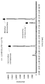
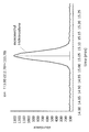
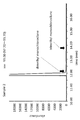
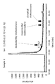
- FIG. 1 It is a chart (measurement chart of mass number 43) obtained by GC / MS-SIM analysis of sample A.
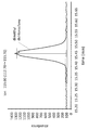
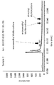
- 6 is a chart (measurement chart having a mass number of 93) obtained by GC / MS-SIM analysis of Sample A.
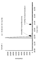
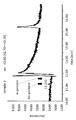
- FIG. 2 is a chart (measurement chart having a mass number of 113) obtained by GC / MS-SIM analysis of sample A.
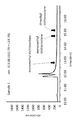
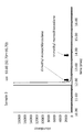
- FIG. It is a chart (measurement chart of mass number 43) obtained by GC / MS-SIM analysis of sample B.
- 6 is a chart (measurement chart having a mass number of 93) obtained by GC / MS-SIM analysis of Sample B.
- FIG. 6 is a chart (measurement chart having a mass number of 93) obtained by GC / MS-SIM analysis of Sample B.
- FIG. 2 is a chart (measurement chart having a mass number of 113) obtained by GC / MS-SIM analysis of Sample B.
- FIG. 2 is a chart (measurement chart having a mass number of 113) obtained by GC / MS-SIM analysis of Sample B.
- FIG. 2 is a chart (measurement chart having a mass number of 113) obtained by GC / MS-SIM analysis of Sample B.
- FIG. 3 is a chart obtained by GC / MS-SIM analysis of Sample 1 (mass number 43). It is the chart obtained by GC / MS-SIM analysis of sample 1 (mass number 93).
- 3 is a chart obtained by GC / MS-SIM analysis of Sample 1 (mass number 113).
- 3 is a chart obtained by GC / MS-SIM analysis of Sample 2 (mass number 43). It is the chart obtained by GC / MS-SIM analysis of sample 2 (mass number 93).
- 3 is a chart obtained by GC / MS-SIM analysis of Sample 2 (mass number 113).
- 6 is a chart obtained by GC / MS-SIM analysis of Sample 3 (mass number 43). It is the chart obtained by GC / MS-SIM analysis of sample 3 (mass number 93).
- 3 is a chart obtained by GC / MS-SIM analysis of Sample 3 (mass number 113).
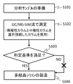
- 6 is a chart obtained by GC-FID analysis of Sample 2. It is a flowchart of the manufacturing method of the polycrystalline silicon which concerns on this invention.
- Chlorosilanes can be obtained, for example, by a direct method using metallurgical grade silicon and hydrogen chloride (see Patent Documents 2 and 3). Also, when polycrystal silicon is produced using tetrachlorosilane or trichlorosilane, which are by-products when obtaining chlorosilanes by the direct method, as raw materials, tetrachlorosilane can be obtained from the exhaust gas at that time. Chlorosilanes can also be obtained by a method of reducing by reacting with hydrogen in the presence of (see Patent Documents 4 and 5).
- the GC-FID method is generally used for measuring impurities in the obtained trichlorosilane. If the purification process of trichlorosilane is appropriate, the impurity content is below the detection limit of the GC-FID method, specifically, The general organic matter is 0.1 ppmw or less, and the methylsilanes is 0.1 ppmw or less.
- the present inventors have studied a method for detecting carbon-containing impurities in trichlorosilane with high sensitivity.
- the detection sensitivity of the carbon-containing impurities is set to GC.
- GC / MS means a gas chromatograph mass spectrometer
- SIM means selected ion monitoring.
- the lower limit of detection of carbon-containing impurities in trichlorosilane is 0.01 ppmw for methylsilanes and 0.05 ppmw for general carbon-containing compounds, which is approximately compared to the GC-FID method. Analysis with 10 times the sensitivity becomes possible. That is, by analyzing the carbon-containing impurities in trichlorosilane by the GC / MS-SIM method, 0.01 ppmw or less for methylsilanes and 0.05 ppmw or less for general carbon-containing compounds (hydrocarbons) were guaranteed. It is possible to produce polycrystalline silicon using trichlorosilane as a raw material.
- the transfer rate is in the range of about 1 to 10%.
- the amount of methyldichlorosilane that can be mixed even when the production of polycrystalline silicon is performed in an environment where the maximum amount is transferred, even when highly purified is 0.01 ppmw or less
- the carbon concentration in the synthesized polycrystalline silicon is 0.048 ppma or less, assuming that 10% of the total amount of carbon is transferred.
- 135.45 is the molecular weight of trichlorosilane, and 12.0 is the atomic weight of C.
- the method for producing high-purity polycrystalline silicon according to the present invention is a method for producing high-purity polycrystalline silicon by CVD using chlorosilanes, and analyzing the amount of carbon-containing impurities by GC / MS-SIM method. Then, the quality is judged, and trichlorosilane that satisfies the conditions used as the judgment criteria is used as a raw material.
- the determination criteria are 0.01 ppmw or less for methylsilanes as carbon-containing impurities and 0.05 ppmw or less for hydrocarbons for the reasons described above.
- Non-Patent Document 1 The method of quantitative analysis by the GC / MS-SIM method has been introduced in Non-Patent Document 1, etc.
- the conditions for analyzing carbon-containing impurities in trichlorosilane in the present invention are, for example, as follows: Is.
- the usual analysis conditions for chlorosilanes can be applied as they are, and as the carrier gas, for example, hydrogen, helium, nitrogen or the like can be used.
- a medium polarity capillary column is preferable for methylsilanes
- a nonpolar capillary column is preferable for hydrocarbons.
- a nonpolar column and a medium polarity column are connected in series.
- nonpolar column or the medium polarity column there are no particular restrictions on the nonpolar column or the medium polarity column, and known ones can be appropriately selected and used. For example, there are products of Agilent Technologies, Varian, Supelco, Restek, GL Science, etc. .
- nonpolar capillary columns include DB-1, DB-5, VF-1, VF-5, SPB-1, SPB-5, Rtx-1, Rtx-5, TC-1, TC- 5 etc. can be used suitably.
- medium polarity capillary columns include DB-17, DB-200, DB-210, DB-225, VF-17, VF-23, VF-200, VF-1701, Select Silane, SBP. -17, SP-2331, Rtx-225, Rtx-1701, TC-17, etc. can be preferably used.
- the oven temperature at the time of separation is in the range of about 20 to 150 ° C., and a good temperature separation program can be established within this temperature range to obtain good separation.
- an electron impact ionization method (EI) can be employed.
- EI electron impact ionization method
- a 70 eV electron beam bombardment may be applied to gas molecules to form monovalent positive ions.
- the ionization current is about 34 to 35 ⁇ A
- the ionization chamber temperature is 200 to 250 ° C.
- the transfer line temperature is 200 to 250 ° C.
- the detector voltage is 1000 to 2000 V as a guide.
- the amount of carbon-containing impurities in the trichlorosilane is previously analyzed by the GC / MS-SIM method. Then, a product that satisfies the conditions set as the judgment criteria is judged as a good product, and this good product is used as a raw material.
- a method for producing polycrystalline silicon by the Siemens method is widely known.
- the method is as follows.
- a silicon core wire serving as a seed crystal of polycrystalline silicon is placed in a CVD reactor and energized to heat it. Further, in a state where the surface temperature of the silicon core wire is maintained at 900 to 1200 ° C., trichlorosilane which is determined to be non-defective by the GC / MS-SIM method is supplied together with hydrogen which is a carrier gas. Trichlorosilane decomposes on the silicon core wire, and polycrystalline silicon grows on the silicon core wire.
- chlorosilanes such as trichlorosilane and tetrachlorosilane are discharged together with hydrogen as exhaust gas, but hydrogen and trichlorosilane are recovered and reused.
- chlorosilanes such as tetrachlorosilane are converted to trichlorosilane and reused (see Patent Documents 4 and 5).
- the detection sensitivity of carbon-containing impurities can be increased by about 10 times compared to the case of using the conventional GC-FID method. It becomes easy to increase the purity of the production raw material trichlorosilane, and as a result, the polycrystalline silicon can be further purified.
- GC conditions Carrier gas: He (1 ml / min)
- 1 to 3 show charts obtained by the above-described GC / MS-SIM analysis.
- 1 is a measurement chart of mass number 43
- FIG. 2 is a measurement chart of mass number 93
- Peaks derived from trimethylsilane, isopentane and n-pentane can be detected by measuring the mass number 43 in the GC / MS-SIM method by comparing with the gas chromatography chart previously obtained by the GC-FID method. It is possible to detect peaks derived from dimethylmonochlorosilane and trimethylmonochlorosilane by measuring mass number 93, and from monomethyldichlorosilane, monomethyltrichlorosilane, dimethyldichlorosilane by measuring mass number 113. It was confirmed that peak detection was possible.
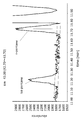
- FIGS. 4 to 9 show charts obtained by GC / MS-SIM analysis.
- 4 is a measurement chart of mass number 43
- FIGS. 5 and 6 are measurement charts of mass number 93
- FIGS. 7 to 9 are measurement charts of mass number 113.
- the detection limit of each component was determined. The results are as follows.
- the detection limit (SN2) was determined by the following formula.
- [SN2] 2 ⁇ (baseline noise width mm) ⁇ (0.1 ppmw / peak abundance height mm)
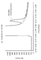
- FIGS. 10 to 12 are charts obtained by GC / MS-SIM analysis of sample 1
- FIGS. 13 to 15 are charts obtained by GC / MS-SIM analysis of sample 2
- FIGS. 16 to 18 are GC / MS of sample 3.
- 3 is a chart obtained by MS-SIM analysis. The quantitative analysis results obtained from these charts are summarized in Table 1 (concentration is ppmw).
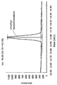
- FIG. 19 is a chart obtained by GC-FID analysis of Sample 2.
- this chart is compared with the charts obtained by the GC / MS-SIM analysis of FIGS. 13 to 15, the peaks (methyldichlorosilane and isopentane) that can be observed with GC / MS-SIM cannot be observed with GC-FID. I understand that.
- FIG. 20 is a flowchart of a method for producing polycrystalline silicon according to the present invention, and this example is a flowchart for producing polycrystalline silicon by the Siemens method using the sample 1 described above as a raw material.
- sample 1 which is trichlorosilane is prepared (S101), and the amount of carbon-containing impurities is analyzed by the GC / MS-SIM method (S102).
- the quality is judged based on the analysis result (S103), and if it is judged as a good product (S103: Yes), it is used as a raw material for producing high-purity polycrystalline silicon by the CVD method (104).
- S103: Yes when it is determined as a defective product
- impurity analysis by the GC / MS-SIM method was performed using a column in which a nonpolar column and a medium polarity column were connected in series as a separation column.
- Sample 1 was determined to be non-defective. Therefore, polycrystalline silicon was produced using the sample 1 by the Siemens method (see Patent Document 1).
- the carbon concentration in the obtained polycrystalline silicon was found to be 0 according to the analysis by the cryogenic FT-IR method (BRUKER-Optics, FT-IR, VERTEX80V, using liquid nitrogen).
- the concentration was as low as less than 0.05 ppma.
- separation of chlorosilanes and hydrocarbons and separation of chlorosilanes and methylsilanes by the GC / MS-SIM method are performed simultaneously by using a column in which a nonpolar column and a medium polarity column are connected in series as a separation column.
- a column in which a nonpolar column and a medium polarity column are connected in series as a separation column is also an advantage of being able to.
Landscapes
- Chemical & Material Sciences (AREA)
- Organic Chemistry (AREA)
- Inorganic Chemistry (AREA)
- Health & Medical Sciences (AREA)
- Life Sciences & Earth Sciences (AREA)
- Engineering & Computer Science (AREA)
- Physics & Mathematics (AREA)
- Medicinal Chemistry (AREA)
- Food Science & Technology (AREA)
- Analytical Chemistry (AREA)
- Biochemistry (AREA)
- General Health & Medical Sciences (AREA)
- General Physics & Mathematics (AREA)
- Immunology (AREA)
- Pathology (AREA)
- Silicon Compounds (AREA)
- Manufacturing & Machinery (AREA)
Abstract
Description
高度に精製したトリクロロシランに、想定される不純物を各2ppmw含むトリクロロシランGC分析用サンプルAを調整し、下記の条件で分析を行った。
キャリアガス:He(1ml/min)
カラム:アジレントテクノロジ社製DB-1の出口側にVarian社製のVF-200を更に直列に連結して使用
インジェクション:スプリット(0.6μL)、23.4psi、150℃
オーブン温度:20~150℃(10℃/minで昇温し、150℃で温度維持)
イオン化エネルギ:70eV
イオン化電流:34μA
イオン源温度:230℃
トランスファライン温度:230℃
検出器電圧:1000~2000V
モニターイオン:イソペンタン、n-ペンタン、テトラメチルシラン、
ジメチルモノクロロシラン、トリメチルモノクロロシラン
、メチルトリクロロシラン、ジメチルジクロロシラン
サイクルタイム:4.3サイクル/秒
図1~3に、上述のGC/MS-SIM分析で得られたチャートを示す。図1は質量数43の計測チャート、図2は質量数93の計測チャート、図3は質量数113の計測チャートである。予めGC-FID法で得ていたガスクロマトグラフィのチャートと比較することにより、GC/MS-SIM法において、質量数43を計測することによりトリメチルシラン、イソペンタン、n-ペンタンに由来するピーク検出が可能であり、質量数93を計測することによりジメチルモノクロロシラン、トリメチルモノクロロシランに由来するピーク検出が可能であり、質量数113を計測することによりモノメチルジクロロシラン、モノメチルトリクロロシラン、ジメチルジクロロシランに由来するピーク検出が可能であることを確認した。
高度に精製したトリクロロシランに、想定される不純物を各0.1ppmw含むトリクロロシランGC分析用サンプルBを調整し、上記と同様の条件で分析を行った。
n-ペンタン:SN2=2(3.5mm)x(0.1ppmw/43mm)=<0.02ppmw
ジクロロモノクロロシラン:SN2=2(2.0mm)x(0.1ppmw/26mm)=<0.02ppmw
トリメチルモノクロロシラン:SN2=2(2.0mm)x(0.1ppmw/46mm)=<0.01ppmw
モノメチルジクロロシラン:SN2=2(1.5mm)x(0.1ppmw/42mm)=<0.01ppmw
モノメチルトリクロロシラン:SN2=2(1.0mm)x(0.1ppmw/50mm)=<0.01ppmw
ジメチルジクロロシラン:SN2=2(1.5mm)x(0.1ppmw/45mm)=<0.01ppmw
蒸留精度の異なるトリクロロシランのサンプルを3種(サンプル1~3)準備し、GC/MS-SIM法とGC-FID法により分析を行って不純物起因のピーク検出感度の比較を行った。分析は上述の条件で行い、絶対検量線法により各成分の定量を行った。

Claims (4)
- クロロシラン類を用いてCVD法により高純度多結晶シリコンを製造する方法であって、GC/MS-SIM法によりメチルジクロロシランとイソペンタンを含む炭素含有不純物量を分析して良否判定を行い、目的とした多結晶シリコンの炭素含有量の許容値を基準として設けられた炭素含有不純物量許容値を基に判定基準とされた条件を満足したトリクロロシランを前記クロロシラン類として用いる、ことを特徴とする高純度多結晶シリコンの製造方法。
- 前記GC/MS-SIM法による分析対象となる前記炭素含有不純物は、メチルジクロロシランとイソペンタンである、請求項1に記載の高純度多結晶シリコンの製造方法。
- 前記判定基準は、前記炭素含有不純物としてのメチルシラン類が0.01ppmw以下、かつ、炭化水素類が0.05ppmw以下である、請求項1又は2に記載の高純度多結晶シリコンの製造方法。
- 前記GC/MS-SIM法による不純物分析は、無極性カラムと中極性カラムを直列に接続したカラムを分離カラムとして用いて成分の分離を行う、
請求項1又は2に記載の高純度多結晶シリコンの製造方法。
Priority Applications (4)
| Application Number | Priority Date | Filing Date | Title |
|---|---|---|---|
| EP13804452.4A EP2862840B1 (en) | 2012-06-14 | 2013-06-13 | Method for producing high-purity polycrystalline silicon |
| CN201380031327.9A CN104395236B (zh) | 2012-06-14 | 2013-06-13 | 高纯度多晶硅的制造方法 |
| US14/407,255 US9355918B2 (en) | 2012-06-14 | 2013-06-13 | Method for producing high-purity polycrystalline silicon |
| KR20157000531A KR20150032859A (ko) | 2012-06-14 | 2013-06-13 | 고순도 다결정 실리콘의 제조 방법 |
Applications Claiming Priority (2)
| Application Number | Priority Date | Filing Date | Title |
|---|---|---|---|
| JP2012-134863 | 2012-06-14 | ||
| JP2012134863A JP5909153B2 (ja) | 2012-06-14 | 2012-06-14 | 高純度多結晶シリコンの製造方法 |
Publications (1)
| Publication Number | Publication Date |
|---|---|
| WO2013187070A1 true WO2013187070A1 (ja) | 2013-12-19 |
Family
ID=49757914
Family Applications (1)
| Application Number | Title | Priority Date | Filing Date |
|---|---|---|---|
| PCT/JP2013/003729 Ceased WO2013187070A1 (ja) | 2012-06-14 | 2013-06-13 | 高純度多結晶シリコンの製造方法 |
Country Status (7)
| Country | Link |
|---|---|
| US (1) | US9355918B2 (ja) |
| EP (2) | EP2862840B1 (ja) |
| JP (1) | JP5909153B2 (ja) |
| KR (1) | KR20150032859A (ja) |
| CN (2) | CN106966395B (ja) |
| MY (1) | MY170224A (ja) |
| WO (1) | WO2013187070A1 (ja) |
Cited By (1)
| Publication number | Priority date | Publication date | Assignee | Title |
|---|---|---|---|---|
| WO2017022515A1 (ja) * | 2015-08-05 | 2017-02-09 | 東亞合成株式会社 | 炭素分析方法 |
Families Citing this family (9)
| Publication number | Priority date | Publication date | Assignee | Title |
|---|---|---|---|---|
| JP6292164B2 (ja) * | 2015-04-30 | 2018-03-14 | 信越半導体株式会社 | シリコン単結晶の製造方法 |
| CN104849366B (zh) * | 2015-05-11 | 2017-12-19 | 中国恩菲工程技术有限公司 | 检测系统及检测方法 |
| JP6343592B2 (ja) | 2015-07-28 | 2018-06-13 | 信越化学工業株式会社 | 多結晶シリコン製造用反応炉及び多結晶シリコンの製造方法 |
| JP6586405B2 (ja) * | 2016-09-28 | 2019-10-02 | 信越化学工業株式会社 | トリクロロシランの精製システムおよび多結晶シリコンの製造方法 |
| WO2019154502A1 (de) * | 2018-02-08 | 2019-08-15 | Wacker Chemie Ag | Verfahren zur klassifizierung von metallurgischem silicium |
| JP6694002B2 (ja) * | 2018-05-21 | 2020-05-13 | 信越化学工業株式会社 | 多結晶シリコンの製造方法 |
| JP6919633B2 (ja) | 2018-08-29 | 2021-08-18 | 信越半導体株式会社 | 単結晶育成方法 |
| CN111289689A (zh) * | 2018-12-07 | 2020-06-16 | 新疆新特新能材料检测中心有限公司 | 多晶硅生产中的尾气中各组分含量的检测方法及检测系统 |
| CN117310033A (zh) * | 2023-09-27 | 2023-12-29 | 内蒙古新特硅材料有限公司 | 一种氯硅烷中碳杂质的检测方法 |
Citations (13)
| Publication number | Priority date | Publication date | Assignee | Title |
|---|---|---|---|---|
| JPS5673617A (en) | 1979-11-17 | 1981-06-18 | Osaka Titanium Seizo Kk | Manufacture of trichlorosilane |
| JPS6036318A (ja) | 1983-07-18 | 1985-02-25 | モトローラ・インコーポレーテツド | トリクロロシラン製造方法及び装置 |
| JPH02208217A (ja) | 1988-12-08 | 1990-08-17 | Elkem As | トリクロルモノシランの製造方法 |
| JPH09169514A (ja) | 1995-12-22 | 1997-06-30 | Tokuyama Corp | 三塩化ケイ素の製造方法 |
| JPH1029813A (ja) | 1995-12-25 | 1998-02-03 | Tokuyama Corp | トリクロロシランの製造方法 |
| JPH1149509A (ja) | 1997-06-03 | 1999-02-23 | Tokuyama Corp | 炭素含有量の少ない多結晶シリコンの製造方法 |
| JP2003172726A (ja) * | 2001-12-07 | 2003-06-20 | Shimadzu Corp | クロマトグラフ質量分析装置 |
| JP2004149351A (ja) | 2002-09-04 | 2004-05-27 | Sumitomo Titanium Corp | クロロシラン及びその精製方法 |
| JP2009062213A (ja) | 2007-09-05 | 2009-03-26 | Shin Etsu Chem Co Ltd | クロロシラン類の精製方法 |
| JP2009062212A (ja) | 2007-09-05 | 2009-03-26 | Shin Etsu Chem Co Ltd | トリクロロシランの製造方法および多結晶シリコンの製造方法 |
| WO2010021339A1 (ja) * | 2008-08-22 | 2010-02-25 | チッソ株式会社 | 四塩化珪素の精製方法 |
| JP2010281699A (ja) * | 2009-06-04 | 2010-12-16 | Canon Anelva Corp | イオン付着質量分析装置(iams)を用いた不分離ピークの定量方法 |
| JP2011184255A (ja) | 2010-03-10 | 2011-09-22 | Shin-Etsu Chemical Co Ltd | トリクロロシランの製造方法 |
Family Cites Families (13)
| Publication number | Priority date | Publication date | Assignee | Title |
|---|---|---|---|---|
| US4374110A (en) * | 1981-06-15 | 1983-02-15 | Motorola, Inc. | Purification of silicon source materials |
| US5444246A (en) * | 1992-09-30 | 1995-08-22 | Shin-Etsu Handotai Co., Ltd. | Determining carbon concentration in silicon single crystal by FT-IR |
| US5445679A (en) * | 1992-12-23 | 1995-08-29 | Memc Electronic Materials, Inc. | Cleaning of polycrystalline silicon for charging into a Czochralski growing process |
| JP3506599B2 (ja) * | 1998-02-04 | 2004-03-15 | Necエレクトロニクス株式会社 | 分析方法 |
| JP2007505477A (ja) * | 2003-07-23 | 2007-03-08 | エーエスエム アメリカ インコーポレイテッド | シリコン−オン−インシュレーター構造及びバルク基板に対するSiGeの堆積 |
| DE102005046703A1 (de) * | 2005-09-29 | 2007-04-05 | Wacker Chemie Ag | Verfahren und Vorrichtung zur Hydrierung von Chlorsilanen |
| DE102007049930B4 (de) * | 2007-10-18 | 2011-04-28 | Universität Hamburg | Oberflächenmodifizierte Hohlraumstrukturen, Verfahren zu deren Herstellung sowie deren Verwendung |
| JPWO2010029894A1 (ja) * | 2008-09-09 | 2012-05-17 | Jnc株式会社 | 高純度結晶シリコン、高純度四塩化珪素およびそれらの製造方法 |
| JP2010217440A (ja) * | 2009-03-16 | 2010-09-30 | Powdertech Co Ltd | 二成分系電子写真現像剤用キャリア及び該キャリアを用いた電子写真現像剤 |
| CN101531674B (zh) * | 2009-04-23 | 2012-02-15 | 嘉兴学院 | 一种甲基氯硅烷的制备方法 |
| DE102010040293A1 (de) * | 2010-09-06 | 2012-03-08 | Wacker Chemie Ag | Verfahren zur Herstellung von polykristallinem Silicium |
| CN102351195A (zh) * | 2011-07-15 | 2012-02-15 | 中国科学院过程工程研究所 | 一种闭路循环生产多晶硅的工艺 |
| CN102286016A (zh) * | 2011-09-15 | 2011-12-21 | 江苏弘博新材料有限公司 | 一种甲基氯硅烷的制备方法 |
-
2012
- 2012-06-14 JP JP2012134863A patent/JP5909153B2/ja active Active
-
2013
- 2013-06-13 US US14/407,255 patent/US9355918B2/en active Active
- 2013-06-13 CN CN201610890923.8A patent/CN106966395B/zh active Active
- 2013-06-13 MY MYPI2014703617A patent/MY170224A/en unknown
- 2013-06-13 EP EP13804452.4A patent/EP2862840B1/en active Active
- 2013-06-13 EP EP16202542.3A patent/EP3170791A1/en not_active Withdrawn
- 2013-06-13 WO PCT/JP2013/003729 patent/WO2013187070A1/ja not_active Ceased
- 2013-06-13 CN CN201380031327.9A patent/CN104395236B/zh active Active
- 2013-06-13 KR KR20157000531A patent/KR20150032859A/ko not_active Withdrawn
Patent Citations (13)
| Publication number | Priority date | Publication date | Assignee | Title |
|---|---|---|---|---|
| JPS5673617A (en) | 1979-11-17 | 1981-06-18 | Osaka Titanium Seizo Kk | Manufacture of trichlorosilane |
| JPS6036318A (ja) | 1983-07-18 | 1985-02-25 | モトローラ・インコーポレーテツド | トリクロロシラン製造方法及び装置 |
| JPH02208217A (ja) | 1988-12-08 | 1990-08-17 | Elkem As | トリクロルモノシランの製造方法 |
| JPH09169514A (ja) | 1995-12-22 | 1997-06-30 | Tokuyama Corp | 三塩化ケイ素の製造方法 |
| JPH1029813A (ja) | 1995-12-25 | 1998-02-03 | Tokuyama Corp | トリクロロシランの製造方法 |
| JPH1149509A (ja) | 1997-06-03 | 1999-02-23 | Tokuyama Corp | 炭素含有量の少ない多結晶シリコンの製造方法 |
| JP2003172726A (ja) * | 2001-12-07 | 2003-06-20 | Shimadzu Corp | クロマトグラフ質量分析装置 |
| JP2004149351A (ja) | 2002-09-04 | 2004-05-27 | Sumitomo Titanium Corp | クロロシラン及びその精製方法 |
| JP2009062213A (ja) | 2007-09-05 | 2009-03-26 | Shin Etsu Chem Co Ltd | クロロシラン類の精製方法 |
| JP2009062212A (ja) | 2007-09-05 | 2009-03-26 | Shin Etsu Chem Co Ltd | トリクロロシランの製造方法および多結晶シリコンの製造方法 |
| WO2010021339A1 (ja) * | 2008-08-22 | 2010-02-25 | チッソ株式会社 | 四塩化珪素の精製方法 |
| JP2010281699A (ja) * | 2009-06-04 | 2010-12-16 | Canon Anelva Corp | イオン付着質量分析装置(iams)を用いた不分離ピークの定量方法 |
| JP2011184255A (ja) | 2010-03-10 | 2011-09-22 | Shin-Etsu Chemical Co Ltd | トリクロロシランの製造方法 |
Non-Patent Citations (2)
| Title |
|---|
| "New Approaches to the Development of GC/MS Selected Ion Monitoring Acquisition and Quantitation Methods", 14 November 2001, EN AGILENT TECHNOLOGIES, INC., pages: 5988 - 4188 |
| See also references of EP2862840A4 |
Cited By (1)
| Publication number | Priority date | Publication date | Assignee | Title |
|---|---|---|---|---|
| WO2017022515A1 (ja) * | 2015-08-05 | 2017-02-09 | 東亞合成株式会社 | 炭素分析方法 |
Also Published As
| Publication number | Publication date |
|---|---|
| EP2862840A4 (en) | 2015-11-11 |
| JP5909153B2 (ja) | 2016-04-26 |
| CN104395236A (zh) | 2015-03-04 |
| US20150170976A1 (en) | 2015-06-18 |
| CN106966395A (zh) | 2017-07-21 |
| US9355918B2 (en) | 2016-05-31 |
| EP2862840A1 (en) | 2015-04-22 |
| MY170224A (en) | 2019-07-10 |
| JP2013256431A (ja) | 2013-12-26 |
| KR20150032859A (ko) | 2015-03-30 |
| EP2862840B1 (en) | 2017-01-25 |
| CN104395236B (zh) | 2016-11-16 |
| EP3170791A1 (en) | 2017-05-24 |
| CN106966395B (zh) | 2019-11-01 |
Similar Documents
| Publication | Publication Date | Title |
|---|---|---|
| JP5909153B2 (ja) | 高純度多結晶シリコンの製造方法 | |
| EP2957543B1 (en) | Method for producing trichlorosilane | |
| US9266742B2 (en) | Method for producing trichlorosilane | |
| JP6184898B2 (ja) | クロロシラン類、クロロシラン類の精製方法、および、シリコン結晶 | |
| TWI582044B (zh) | 藉由裂開如八氯三矽烷之高級多氯矽烷製造六氯二矽烷的方法 | |
| KR20150144760A (ko) | 옥타클로로트리실란을 제조하는 방법 및 장치 | |
| JP3878278B2 (ja) | 燐含有量の少ない多結晶シリコンの製造方法 | |
| US20180086645A1 (en) | Trichlorosilane purification system and method for producing polycrystalline silicon | |
| JP7506836B2 (ja) | 精製トリクロロシランの製造方法 | |
| CN106488884A (zh) | 氯硅烷的纯化方法 | |
| US11691884B2 (en) | Method of classifying metallurgical silicon | |
| Operti et al. | Gas-phase ion chemistry in silane/propyne mixtures |
Legal Events
| Date | Code | Title | Description |
|---|---|---|---|
| 121 | Ep: the epo has been informed by wipo that ep was designated in this application |
Ref document number: 13804452 Country of ref document: EP Kind code of ref document: A1 |
|
| REEP | Request for entry into the european phase |
Ref document number: 2013804452 Country of ref document: EP |
|
| WWE | Wipo information: entry into national phase |
Ref document number: 2013804452 Country of ref document: EP |
|
| WWE | Wipo information: entry into national phase |
Ref document number: 14407255 Country of ref document: US |
|
| NENP | Non-entry into the national phase |
Ref country code: DE |
|
| ENP | Entry into the national phase |
Ref document number: 20157000531 Country of ref document: KR Kind code of ref document: A |