WO2013190838A1 - Substrat tft, procédé pour sa production, dispositif d'affichage el organique et procédé de fabrication d'un dispositif d'affichage el organique - Google Patents
Substrat tft, procédé pour sa production, dispositif d'affichage el organique et procédé de fabrication d'un dispositif d'affichage el organique Download PDFInfo
- Publication number
- WO2013190838A1 WO2013190838A1 PCT/JP2013/003823 JP2013003823W WO2013190838A1 WO 2013190838 A1 WO2013190838 A1 WO 2013190838A1 JP 2013003823 W JP2013003823 W JP 2013003823W WO 2013190838 A1 WO2013190838 A1 WO 2013190838A1
- Authority
- WO
- WIPO (PCT)
- Prior art keywords
- film
- layer
- opening
- insulating layer
- tft substrate
- Prior art date
- Legal status (The legal status is an assumption and is not a legal conclusion. Google has not performed a legal analysis and makes no representation as to the accuracy of the status listed.)
- Ceased
Links
Images


Classifications
-
- H—ELECTRICITY
- H10—SEMICONDUCTOR DEVICES; ELECTRIC SOLID-STATE DEVICES NOT OTHERWISE PROVIDED FOR
- H10P—GENERIC PROCESSES OR APPARATUS FOR THE MANUFACTURE OR TREATMENT OF DEVICES COVERED BY CLASS H10
- H10P50/00—Etching of wafers, substrates or parts of devices
- H10P50/20—Dry etching; Plasma etching; Reactive-ion etching
- H10P50/28—Dry etching; Plasma etching; Reactive-ion etching of insulating materials
- H10P50/282—Dry etching; Plasma etching; Reactive-ion etching of insulating materials of inorganic materials
- H10P50/283—Dry etching; Plasma etching; Reactive-ion etching of insulating materials of inorganic materials by chemical means
-
- H—ELECTRICITY
- H10—SEMICONDUCTOR DEVICES; ELECTRIC SOLID-STATE DEVICES NOT OTHERWISE PROVIDED FOR
- H10D—INORGANIC ELECTRIC SEMICONDUCTOR DEVICES
- H10D30/00—Field-effect transistors [FET]
- H10D30/01—Manufacture or treatment
- H10D30/021—Manufacture or treatment of FETs having insulated gates [IGFET]
- H10D30/031—Manufacture or treatment of FETs having insulated gates [IGFET] of thin-film transistors [TFT]
- H10D30/0312—Manufacture or treatment of FETs having insulated gates [IGFET] of thin-film transistors [TFT] characterised by the gate electrodes
- H10D30/0316—Manufacture or treatment of FETs having insulated gates [IGFET] of thin-film transistors [TFT] characterised by the gate electrodes of lateral bottom-gate TFTs comprising only a single gate
-
- H—ELECTRICITY
- H10—SEMICONDUCTOR DEVICES; ELECTRIC SOLID-STATE DEVICES NOT OTHERWISE PROVIDED FOR
- H10D—INORGANIC ELECTRIC SEMICONDUCTOR DEVICES
- H10D30/00—Field-effect transistors [FET]
- H10D30/01—Manufacture or treatment
- H10D30/021—Manufacture or treatment of FETs having insulated gates [IGFET]
- H10D30/031—Manufacture or treatment of FETs having insulated gates [IGFET] of thin-film transistors [TFT]
- H10D30/0321—Manufacture or treatment of FETs having insulated gates [IGFET] of thin-film transistors [TFT] comprising silicon, e.g. amorphous silicon or polysilicon
-
- H—ELECTRICITY
- H10—SEMICONDUCTOR DEVICES; ELECTRIC SOLID-STATE DEVICES NOT OTHERWISE PROVIDED FOR
- H10D—INORGANIC ELECTRIC SEMICONDUCTOR DEVICES
- H10D30/00—Field-effect transistors [FET]
- H10D30/60—Insulated-gate field-effect transistors [IGFET]
- H10D30/67—Thin-film transistors [TFT]
- H10D30/6704—Thin-film transistors [TFT] having supplementary regions or layers in the thin films or in the insulated bulk substrates for controlling properties of the device
-
- H—ELECTRICITY
- H10—SEMICONDUCTOR DEVICES; ELECTRIC SOLID-STATE DEVICES NOT OTHERWISE PROVIDED FOR
- H10D—INORGANIC ELECTRIC SEMICONDUCTOR DEVICES
- H10D30/00—Field-effect transistors [FET]
- H10D30/60—Insulated-gate field-effect transistors [IGFET]
- H10D30/67—Thin-film transistors [TFT]
- H10D30/674—Thin-film transistors [TFT] characterised by the active materials
- H10D30/6755—Oxide semiconductors, e.g. zinc oxide, copper aluminium oxide or cadmium stannate
- H10D30/6756—Amorphous oxide semiconductors
-
- H—ELECTRICITY
- H10—SEMICONDUCTOR DEVICES; ELECTRIC SOLID-STATE DEVICES NOT OTHERWISE PROVIDED FOR
- H10D—INORGANIC ELECTRIC SEMICONDUCTOR DEVICES
- H10D86/00—Integrated devices formed in or on insulating or conducting substrates, e.g. formed in silicon-on-insulator [SOI] substrates or on stainless steel or glass substrates
- H10D86/01—Manufacture or treatment
- H10D86/021—Manufacture or treatment of multiple TFTs
- H10D86/0231—Manufacture or treatment of multiple TFTs using masks, e.g. half-tone masks
-
- H—ELECTRICITY
- H10—SEMICONDUCTOR DEVICES; ELECTRIC SOLID-STATE DEVICES NOT OTHERWISE PROVIDED FOR
- H10D—INORGANIC ELECTRIC SEMICONDUCTOR DEVICES
- H10D86/00—Integrated devices formed in or on insulating or conducting substrates, e.g. formed in silicon-on-insulator [SOI] substrates or on stainless steel or glass substrates
- H10D86/40—Integrated devices formed in or on insulating or conducting substrates, e.g. formed in silicon-on-insulator [SOI] substrates or on stainless steel or glass substrates characterised by multiple TFTs
- H10D86/421—Integrated devices formed in or on insulating or conducting substrates, e.g. formed in silicon-on-insulator [SOI] substrates or on stainless steel or glass substrates characterised by multiple TFTs having a particular composition, shape or crystalline structure of the active layer
- H10D86/423—Integrated devices formed in or on insulating or conducting substrates, e.g. formed in silicon-on-insulator [SOI] substrates or on stainless steel or glass substrates characterised by multiple TFTs having a particular composition, shape or crystalline structure of the active layer comprising semiconductor materials not belonging to the Group IV, e.g. InGaZnO
-
- H—ELECTRICITY
- H10—SEMICONDUCTOR DEVICES; ELECTRIC SOLID-STATE DEVICES NOT OTHERWISE PROVIDED FOR
- H10D—INORGANIC ELECTRIC SEMICONDUCTOR DEVICES
- H10D86/00—Integrated devices formed in or on insulating or conducting substrates, e.g. formed in silicon-on-insulator [SOI] substrates or on stainless steel or glass substrates
- H10D86/40—Integrated devices formed in or on insulating or conducting substrates, e.g. formed in silicon-on-insulator [SOI] substrates or on stainless steel or glass substrates characterised by multiple TFTs
- H10D86/60—Integrated devices formed in or on insulating or conducting substrates, e.g. formed in silicon-on-insulator [SOI] substrates or on stainless steel or glass substrates characterised by multiple TFTs wherein the TFTs are in active matrices
-
- H—ELECTRICITY
- H10—SEMICONDUCTOR DEVICES; ELECTRIC SOLID-STATE DEVICES NOT OTHERWISE PROVIDED FOR
- H10D—INORGANIC ELECTRIC SEMICONDUCTOR DEVICES
- H10D99/00—Subject matter not provided for in other groups of this subclass
-
- H—ELECTRICITY
- H10—SEMICONDUCTOR DEVICES; ELECTRIC SOLID-STATE DEVICES NOT OTHERWISE PROVIDED FOR
- H10K—ORGANIC ELECTRIC SOLID-STATE DEVICES
- H10K59/00—Integrated devices, or assemblies of multiple devices, comprising at least one organic light-emitting element covered by group H10K50/00
- H10K59/10—OLED displays
- H10K59/12—Active-matrix OLED [AMOLED] displays
- H10K59/1201—Manufacture or treatment
-
- H—ELECTRICITY
- H10—SEMICONDUCTOR DEVICES; ELECTRIC SOLID-STATE DEVICES NOT OTHERWISE PROVIDED FOR
- H10P—GENERIC PROCESSES OR APPARATUS FOR THE MANUFACTURE OR TREATMENT OF DEVICES COVERED BY CLASS H10
- H10P50/00—Etching of wafers, substrates or parts of devices
- H10P50/73—Etching of wafers, substrates or parts of devices using masks for insulating materials
-
- H—ELECTRICITY
- H10—SEMICONDUCTOR DEVICES; ELECTRIC SOLID-STATE DEVICES NOT OTHERWISE PROVIDED FOR
- H10K—ORGANIC ELECTRIC SOLID-STATE DEVICES
- H10K59/00—Integrated devices, or assemblies of multiple devices, comprising at least one organic light-emitting element covered by group H10K50/00
- H10K59/80—Constructional details
- H10K59/805—Electrodes
- H10K59/8051—Anodes
- H10K59/80516—Anodes combined with auxiliary electrodes, e.g. ITO layer combined with metal lines
Definitions
- the technology disclosed herein relates to a TFT (Thin Film Transistor) substrate and a manufacturing method of the TFT substrate, an organic EL (Electro-Luminescence) display device driven by the TFT, and a manufacturing method of the organic EL display device.
- TFT Thin Film Transistor
- organic EL Electro-Luminescence
- the conventional technology has a problem that it is difficult to realize a TFT substrate having desired performance.
- a TFT substrate manufacturing method in which a TFT including an oxide semiconductor layer is formed, and a step of forming an insulating layer so as to cover the TFT And forming an opening in the insulating layer.
- the insulating layer includes a first film, a second film that is an aluminum oxide film provided on the first film, and a second film
- a step of forming an opening in the insulating layer includes a step of forming a resist pattern on the third film, and a step of forming a resist pattern on the third layer.
- a step of processing the film by dry etching and a step of processing the second film by wet etching a step of processing the second film by wet etching.
- One embodiment of a TFT substrate that solves the above problem includes an insulating layer provided with an opening, and an electrode provided continuously in the opening and on the insulating layer.
- a film, a second film provided on the first film, and a third film provided on the second film, and at least the cross section of the three films in the opening is a forward tapered shape
- an aspect of the second TFT substrate manufacturing method that solves the above problem includes a step of forming an insulating layer, a step of forming an opening in the insulating layer, and the inside of the opening and the insulating layer continuously.
- a step of processing the second film by wet etching and a step of processing the first film by dry etching, and the step of processing the third film by dry etching The cross section of the film is a forward tapered shape.
- a TFT substrate having desired performance can be realized.
- FIG. 1 is an exploded perspective view showing a schematic configuration of the organic EL display device according to the first embodiment.
- FIG. 2 is a view showing a part of a cross section taken along line 2-2 in FIG.
- FIG. 3 is a view showing a part of a cross section taken along line 3-3 in FIG.
- FIG. 4 is a manufacturing flowchart of the organic EL display device according to the first embodiment.
- FIG. 5 is a manufacturing flowchart of the TFT substrate in the first embodiment.
- FIG. 6 is a diagram showing a schematic cross section after the formation of the gate electrode in the manufacturing process of the TFT substrate in the first embodiment.
- FIG. 7 is a diagram showing a schematic cross section after the formation of the gate insulating film in the manufacturing process of the TFT substrate in the first embodiment.
- FIG. 8 is a diagram showing a schematic cross section after the formation of the semiconductor layer in the manufacturing process of the TFT substrate in the first embodiment.
- FIG. 9 is a diagram showing a schematic cross section after the formation of the first insulating layer in the manufacturing process of the TFT substrate in the first embodiment.
- FIG. 10 is a diagram showing a schematic cross section after the formation of the first electrode in the manufacturing process of the TFT substrate in the first embodiment.
- FIG. 11 is a diagram showing a schematic cross section after the formation of the protective layer in the manufacturing process of the TFT substrate in the first embodiment.
- FIG. 12 is a diagram showing a schematic cross section after the formation of the second electrode in the manufacturing process of the TFT substrate in the first embodiment.
- FIG. 13 is a diagram showing a schematic cross section after the formation of the second insulating layer in the manufacturing process of the TFT substrate in the first embodiment.
- FIG. 14 is a manufacturing flow diagram of the EL device unit according to the first embodiment.
- FIG. 15 is a diagram showing a schematic cross section after the planarization layer is formed in the manufacturing process of the EL device portion in the first embodiment.
- FIG. 16 is a diagram showing a schematic cross section after formation of the reflective anode in the manufacturing process of the EL device portion in the first embodiment.
- FIG. 17 is a diagram showing a schematic cross section after forming the hole injection layer in the manufacturing process of the EL device portion in the first embodiment.
- FIG. 18 is a diagram showing a schematic cross section after forming a bank in the manufacturing process of the EL device portion in the first embodiment.
- FIG. 19 is a diagram showing a schematic cross section after the formation of the electronic block layer in the manufacturing process of the EL device portion in the first embodiment.
- FIG. 20 is a diagram showing a schematic cross section after the formation of the light emitting layer in the manufacturing process of the EL device portion in the first embodiment.
- FIG. 21 is a diagram showing a schematic cross section after formation of the electron injection layer in the manufacturing process of the EL device portion in the first embodiment.
- FIG. 22 is a diagram showing a schematic cross section after forming the cathode in the manufacturing process of the EL device portion in the first embodiment.
- FIG. 23 is a diagram showing a schematic cross section after forming the sealing layer in the manufacturing process of the EL device portion in the first embodiment.
- FIG. 24 is a diagram showing a schematic cross section around the opening of the first insulating layer of the TFT substrate in the first embodiment.
- FIG. 25 is a diagram showing a flow of forming the first insulating layer in the first embodiment.
- FIG. 26 is a diagram showing a flow of forming the opening of the first insulating layer and the first electrode.
- FIG. 27 is a diagram showing a schematic cross section after forming a resist pattern in the process of forming the opening of the first insulating layer in the first embodiment.
- FIG. 28 is a diagram showing a schematic cross section after processing the third film in the process of forming the opening of the first insulating layer in the first embodiment.
- FIG. 29 is a diagram showing a schematic cross section after processing the second film in the process of forming the opening of the first insulating layer in the first embodiment.
- FIG. 30 is a diagram showing a schematic cross section after processing the first film in the process of forming the opening of the first insulating layer in the first embodiment.
- FIG. 31 is a diagram showing a schematic cross section after resist removal in the process of forming the opening of the first insulating layer in the first embodiment.
- FIG. 32 is a diagram showing a schematic cross section of the first electrode formation step in the first embodiment.
- FIG. 33 is a cross-sectional SEM image of the periphery of the first opening in the example of the first embodiment.
- FIG. 34 is a diagram showing a schematic cross section around the opening of the first insulating layer of the TFT substrate in the second embodiment.
- FIG. 35 is a diagram showing a flow of forming the first insulating layer in the second embodiment.
- FIG. 36 is a diagram showing a flow of forming the opening of the first insulating layer and the first electrode in the second embodiment.
- FIG. 37 is a diagram showing a schematic cross section after forming a resist pattern in the process of forming the opening of the first insulating layer in the second embodiment.
- FIG. 38 is a diagram showing a schematic cross section after processing the third film in the process of forming the opening of the first insulating layer in the second embodiment.
- FIG. 39 is a diagram showing a schematic cross section after processing the second film in the process of forming the opening of the first insulating layer in the second embodiment.
- FIG. 40 is a diagram showing a schematic cross section when the first film is processed in the process of forming the opening of the first insulating layer in the second embodiment.
- FIG. 41 is a diagram showing a schematic cross section after removing the resist in the process of forming the opening of the first insulating layer in the second embodiment.
- FIG. 42 is a diagram showing a schematic cross section of the first electrode forming step in the second embodiment.
- FIG. 43 is a diagram showing a schematic cross section around the opening of the first insulating layer of the TFT substrate in a modification of the second embodiment.
- FIG. 44 is a diagram showing a schematic cross section after resist pattern formation in the process of forming the opening of the first insulating layer in the modification of the second embodiment.
- FIG. 45 is a diagram showing a schematic cross-section after processing the fourth film and the third film in the process of forming the opening of the first insulating layer in the modification of the second embodiment.
- FIG. 46 is a diagram showing a schematic cross section after processing the second film in the process of forming the opening of the first insulating layer in the modification of the second embodiment.
- FIG. 47 is a diagram showing a schematic cross section after the first film is processed in the process of forming the opening of the first insulating layer in the modification of the second embodiment.
- FIG. 48 is a diagram showing a schematic cross section after removing the resist in the process of forming the opening of the first insulating layer in the modification of the second embodiment.
- FIG. 49 is a diagram showing a schematic cross section of the first electrode forming step in the modification of the second embodiment.
- FIG. 50 is a cross-sectional SEM image around the opening of the first opening in the example of the second embodiment.
- FIG. 51 is a diagram showing a schematic cross section around the opening of the first insulating layer in another modification of the second embodiment.
- FIG. 52 is a diagram showing a schematic cross section of the first electrode in a modification.
- the TFT substrate has an electrode that is electrically connected to a layer provided below the insulating layer through an opening provided in the insulating layer.
- an aluminum oxide film (alumina film) is used as an insulating layer covering the TFT in order to suppress diffusion of hydrogen and oxygen into the oxide semiconductor layer.
- an insulating layer having a three-layer structure of a silicon oxide film, an aluminum oxide film, and a silicon oxide film is used as an etching stopper layer for the oxide semiconductor layer, which also serves as an insulating layer for the oxide semiconductor layer and the electrode. It may be formed to cover. In this case, an opening is formed in the insulating layer in order to enable conduction between the electrode and the oxide semiconductor layer.
- the aluminum oxide film of the insulating layer is processed by wet etching or dry etching.
- an alkaline solution having a high etching rate is used as the wet etching solution.
- the alkaline solution has an action of removing the resist pattern (resist film). Therefore, if a resist pattern is provided directly on the aluminum oxide film when processing the aluminum oxide film, the resist pattern is peeled off by an alkaline solution during wet etching, and the function as a mask for the resist pattern is impaired. May not be processed into a desired shape. For this reason, until now, it has been difficult to use an alkaline solution as a wet etching solution for processing an aluminum oxide film. That is, there is a problem that the throughput is low when the insulating layer is processed.
- the method of processing the aluminum oxide film by dry etching is not suitable for mass production because the etching selectivity with the lower layer is difficult to take.
- the insulating layer has a three-layer structure of a silicon oxide film, an aluminum oxide film, and a silicon oxide film, it is difficult to obtain an etching selectivity between the aluminum oxide film and the underlying silicon oxide film.
- the present disclosure has been made in view of such problems, and provides a TFT substrate capable of suppressing a decrease in throughput even when wet etching is performed on an insulating layer containing aluminum oxide, a manufacturing method thereof, and the like. Is the first purpose.
- the TFT substrate has a problem that the electrode is disconnected at the end of the opening provided in the insulating layer.
- the present disclosure has been made in view of such problems, and a second object of the present disclosure is to provide a TFT substrate capable of suppressing disconnection of an electrode at an end of an opening of an insulating layer, a manufacturing method thereof, and the like. .
- a first TFT substrate manufacturing method is a TFT substrate manufacturing method in which a TFT including an oxide semiconductor layer is formed, and is insulated so as to cover the TFT.
- a step of forming a layer and a step of forming an opening in the insulating layer, wherein the insulating layer is a first film and a second film that is an aluminum oxide film provided on the first film And a step of forming an opening in the insulating layer, the step of forming a resist pattern on the third film.
- an aspect of the TFT substrate includes an insulating layer provided with an opening, and an electrode provided continuously in the opening and on the insulating layer. Includes a first film, a second film provided on the first film, and a third film provided on the second film, and a cross-section of at least the three films in the opening Has a forward tapered shape.
- one aspect of a method for manufacturing the second TFT substrate includes a step of forming an insulating layer, a step of forming an opening in the insulating layer, an inside of the opening, and the insulating layer.
- Forming an electrode continuously, and forming the insulating layer includes forming a first film, forming a second film on the first film, Forming a third film on the second film, and forming the opening in the insulating layer includes forming a resist pattern on the third film and dry etching the third film.
- the step of processing the third film by dry etching the step of processing the second film by dry etching, and the step of processing the first film by dry etching.
- the cross section of the third film in FIG. Characterized in that.
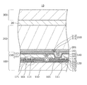
- the disclosed organic EL display device 10 has a configuration in which a TFT substrate 100, an EL device unit 200, and a color filter substrate 300 are laminated. The EL device unit 200 and the color filter substrate 300 are bonded together by the bonding layer 20.
- the configurations of the EL device unit 200 and the color filter substrate are omitted as appropriate.
- the configuration of the TFT substrate 100 is omitted as appropriate.
- the TFT substrate 100 has a plurality of TFT portions 170. As will be described later, each TFT portion 170 has at least two TFTs. The plurality of TFT portions 170 are arranged in a matrix. A signal is supplied to each TFT portion 170 through the gate wiring 180 and the source wiring 190.
- the EL device unit 200 includes a light emitting layer 240.
- the light emitting layer 240 emits light by recombination of holes injected from the anode 210 and electrons injected from the cathode 260.
- the color filter substrate 300 includes a filter 320 provided on the glass substrate 310.
- the filter 320 includes a red filter 321, a green filter 322, and a blue filter 323.
- the red filter 321 transmits red light emitted from the EL device unit 200.
- the green filter 322 transmits the green light emitted from the EL device unit 200.
- the blue filter 323 transmits blue light emitted from the EL device unit 200. That is, the disclosed organic EL display device 10 is a top emission type.
- the TFT substrate is not formed in the direction of extracting light. Therefore, the top emission type can increase the aperture ratio compared to the bottom emission type. In other words, the emission efficiency is further improved in the top emission type.
- the TFT substrate 100 has a plurality of TFT portions 170 on a glass substrate 110.
- Each TFT portion 170 includes a switching TFT 171 and a driving TFT 172.
- the switching TFT 171 switches on / off of the driving TFT 172.
- the driving TFT 172 controls the current supplied to the EL device unit 200.
- the gate electrode 101 is connected to the gate wiring 180.
- the first electrode 130 is connected to the source wiring 190.
- the switching TFT 171 When a gate signal is input to the gate wiring 180, the switching TFT 171 is turned on. Then, charges supplied through the source wiring 190 are accumulated in a capacitor (not shown). The conductance of the driving TFT 172 is continuously changed by the electric charge accumulated in the capacitor (not shown). Therefore, a driving current for causing the EL device unit 200 to emit light so as to obtain a desired luminance can be supplied to the EL device unit 200.
- the disclosed TFT portion 170 is a bottom gate type.
- the gate electrode 101 has a structure in which a Cu (copper) film is stacked on a Mo (molybdenum) film provided on the glass substrate 110.
- the gate electrode 101 is covered with a gate insulating film (gate oxide film) 102.
- the gate insulating film 102 has a structure in which SiO 2 (silicon dioxide) is stacked on SiN (silicon nitride).
- SiO 2 silicon dioxide
- SiN silicon nitride
- a semiconductor layer 111 is provided over the gate insulating film 102.
- a transparent amorphous oxide semiconductor (TAOS), amorphous silicon, or the like is used for the semiconductor layer 111.
- TAOS transparent amorphous oxide semiconductor
- An example of a material for TAOS is a-InGaZnO 4 (amorphous-indium gallium zinc oxide).
- the semiconductor layer 111 is covered with the first insulating layer 120.
- the first insulating layer 120 has a three-layer structure, and includes a first film 121, a second film 122, and a third film 123.
- the first insulating layer 120 is an insulating layer for insulating and separating the semiconductor layer 111 and the first electrode 130. Further, the first insulating layer 120 on the semiconductor layer 111 functions as an etching stopper layer. The configuration of the first insulating layer 120 will be described in detail later.
- the first electrode 130 is connected to the semiconductor layer 111 through the opened portion (opening).
- the first electrode 130 connected to the right side (drain side) of the switching TFT 171 as viewed in the drawing is connected to the gate electrode 101 of the driving TFT 172.
- Cu is used for the first electrode 130.
- the first electrode 130 is covered with a protective layer 140.
- the protective layer 140 has a stacked structure of a first protective layer 141 and a second protective layer 142.
- SiO 2 is used for the first protective layer 141.
- SiN is used for the second protective layer 142.
- a part of the protective layer 140 is opened.
- a second electrode 150 is provided on the protective layer 140.
- the second electrode 150 has a stacked structure of a lower layer electrode 151 and an upper layer electrode 152.
- the second electrode 150 is connected to the first electrode 130 on the left side (source side) of the driving TFT 172 as viewed in the drawing.
- ITO Indium Tin Oxide
- Cu is used for the upper layer electrode 152.
- the second electrode 150 is covered with the second insulating layer 161. A part of the second insulating layer 161 is opened.
- the EL device unit 200 is connected to the TFT substrate 100 through a region opened in a part of the planarization layer 201.
- an anode 210 composed of an upper layer anode 212 and a lower layer anode 211 is connected to the TFT substrate 100.
- the planarization layer 201 is provided on the TFT substrate 100. That is, the unevenness generated in the TFT substrate 100 is alleviated by the planarization layer 201.
- a resin is used for the planarizing layer 201.
- the anode 210 covers the planarization layer 201.
- the opened region of the planarization layer 201 is filled with a part of the anode 210.
- the anode 210 has a laminated structure of a lower layer anode 211 and an upper layer anode 212.
- an aluminum alloy is used for the lower layer anode 211.
- IZO Indium Zinc Oxide
- the anode 210 has a function of reflecting light emitted from the light emitting layer 240. This is to obtain higher luminous efficiency in the top emission type organic EL display device.
- the hole injection layer 231 covers the anode 210.
- the hole injection layer 231 injects holes into the light emitting layer 240.
- the ionization energy of the hole injection layer 231 is selected to be between the work function of the anode 210 and the ionization energy of the light emitting layer 240.
- an organic material such as phthalocyanine, oligoamine, dendrimer amine, or polythiophene, or an inorganic material such as a metal oxide is used.
- a tungsten oxide film is used for the hole injection layer 231.
- the electron blocking layer 232 covers the hole injection layer 231.
- the electron blocking layer 232 suppresses electrons injected from the electron injection layer 251 described later from reaching the hole injection layer 231.
- the ionization energy of the electron block layer 232 is larger than the ionization energy of the light emitting layer 240.
- a polymer material is used for the electron block layer 232.
- the light emitting layer 240 includes a red light emitting layer 241 that emits red light, a green light emitting layer 242 that emits green light, and a blue light emitting layer 243 that emits blue light. As shown in FIG. 3, each of the red light emitting layer 241, the green light emitting layer 242 and the blue light emitting layer 243 is provided in a region partitioned by the bank 220. The light emitting layer 240 is sandwiched between an electron block layer 232 and an electron injection layer 251 described later.
- Both the low molecular weight material and the high molecular weight material can be used for the light emitting layer 240.
- the distinction between low molecular weight materials and high molecular weight materials is not necessarily strict.
- a material having a large molecular weight with a repeating unit of a molecular structure is called a polymer material.
- the molecular weight of the polymer material is approximately 10,000 or more.
- the polymeric material has a molecular weight distribution. Low molecular weight materials usually do not have a molecular weight distribution.
- the light emitting layer 240 is a layer that provides a field where electrons and holes are recombined.
- the light emitting layer 240 includes a host and a dopant that functions as an emission center when electrons and holes are recombined.
- anthracene for example, anthracene, amine, diamine, styryl, silole, azole, polyphenyl and the like are used.
- Examples of the anthracene system include diphenylanthracene derivatives or dimers thereof.
- Examples of the diamine type include biscarbazole.
- Examples of the styryl group include distyrylarylene and styrylamine.
- Silole is a material having a five-membered ring containing silicon (Si). That is, the silole system is one type of electron-deficient ring.
- Examples of azoles include oxazole, oxadiazole, benzimidazole, and the like.
- Examples of the polyphenyl group include terphenyl, quarterphenyl, kinkphenyl, and sexiphenyl.
- the dopant As the dopant, a material having an energy gap smaller than that of the host is selected.
- the dopant is usually added at a concentration of about 0.5 to 5 mol%. The amount of dopant added is adjusted to reduce the effect of concentration quenching. In the light emitting layer 240, the dopant becomes the emission center. Therefore, in general, the EL spectrum of the light emitting layer 240 is the same as the photoluminescence of the dopant.
- Examples of the dopant having a red emission center include cyanomethylenepyran, dicyano, phenoxazone, and thioxanthene.
- Examples of the dopant having a blue emission center include styryl and condensed polycyclic aromatic ring systems.
- Examples of the dopant having a green emission center include a coumarin type and a quinacridone type.
- the electron injection layer 251 covers the light emitting layer 240 and the bank 220.
- the electron injection layer 251 injects electrons into the light emitting layer 240.
- the electron affinity of the electron injection layer 251 is selected to be between the work function of the cathode 260 described later and the electron affinity of the light emitting layer 240.
- an organic material such as a metal chelate, a phenanthroline, an oxadiazole, or a triazole
- an inorganic material such as an alkali metal compound, an alkaline earth metal compound, or the like is used.
- the cathode 260 covers the electron injection layer 251. In the top emission type organic EL display device, it is desired to increase the visible light transmittance of the display surface side electrode (that is, the cathode 260).
- a transparent conductive material such as ITO or IZO is used.
- the cathode 260 may be a laminated film in which a metal film is provided on a transparent conductive material film. For example, silver (Ag), aluminum (Al), or the like is used for the metal film.
- the sealing layer 270 covers the cathode 260.
- moisture derived from the environment, moisture due to cleaning, and the like are likely to enter the EL device portion 200, and peeling of the layer occurs due to the entering moisture. There is. As a result, defects such as failure to obtain normal light emission tend to occur. Therefore, the sealing layer 270 is preferably provided.
- sealing layer 270 organic materials such as polyparaxylene and fluororesin, oxide materials such as SiO 2 , GeO (germanium oxide), Al 2 O 3 (aluminum oxide), SiON (silicon oxynitride), SiN, etc. Nitride materials are used. Note that the sealing layer 270 may have a structure in which a plurality of types of materials are stacked. In the disclosed EL device unit 200, SiN is used as an example.
- the color filter substrate 300 changes the emission color by utilizing light absorption. In other words, the color purity is improved by transmitting light through the color filter substrate 300.
- the filter 320 adjusts the wavelength of transmitted light with a pigment or the like.
- the method for manufacturing the organic EL display device 10 includes a step of manufacturing the TFT substrate 100 (step 1), a step of manufacturing the EL device unit 200 (step 2), and the color filter substrate 300. Including a step (step 3).
- step 1 The process for producing the TFT substrate 100 (step 1) and the process for producing the EL device unit 200 (step 2) will be described in detail later as a manufacturing method of the TFT substrate 100 and a manufacturing method of the EL device unit 200.
- the EL device unit 200 and the color filter substrate 300 are bonded together by the bonding layer 20, as shown in FIG.
- the bonding layer 20 for example, a UV curable resin is used.
- the thickness of the bonding layer 20 is about 10 ⁇ m to 30 ⁇ m. A method for creating the color filter substrate 300 will be described later.
- the TFT substrate 100 is covered with the planarization layer 201 partially opened. Therefore, it is not easy to attach the TFT device 100 after separately manufacturing only the EL device portion 200. On the other hand, after the color filter substrate 300 is separately manufactured, the color filter substrate 300 and the EL device unit 200 can be easily bonded.
- the manufacturing method of the TFT substrate 100 includes a step of forming the gate electrode 101 (step 11), a step of forming the gate insulating film 102 (step 12), and the semiconductor layer 111. Step of forming (Step 13), Step of forming the first insulating layer 120 (Step 14), Step of forming the first electrode 130 (Step 15), Step of forming the protective layer 140 (Step 16) And a step of forming the second electrode 150 (step 17) and a step of forming the second insulating layer 161 (step 18).
- the disclosed TFT substrate 100 is thus manufactured by the steps 11 to 18.
- Step 11 As shown in FIG. 6, in step 11, the gate electrode 101 is formed on the glass substrate 110.
- a Mo film and a Cu film are sequentially deposited on the glass substrate 110 by sputtering.
- the total film thickness of the Mo film and the Cu film is about 50 nm to 150 nm.
- a gate electrode 101 having a predetermined pattern is formed by photolithography and etching using a resist.
- a gate insulating film 102 covering the gate electrode 101 is formed.
- the SiO 2 film is formed to a thickness of about 100 nm to 300 nm by parallel plate type plasma CVD (Chemical Vapor Deposition).
- SiH 4 and N 2 O are used as the material.
- the plasma is generated by applying a high frequency of 13.56 MHz, for example.
- SiH 4 and N 2 O are decomposed in the plasma, and cluster-like SiO 2 is generated.
- SiO 2 is deposited on the glass substrate 110 by self-bias generated in plasma.
- step 13 As shown in FIG. 8, in step 13, the semiconductor layer 111 is formed on the gate insulating film 102.
- a sputtering method is used as an example.
- a target material having a composition ratio In: Ga: Zn of 1: 1: 1 is used.
- a-InGaZnO 4 is formed.
- the film thickness is, for example, about 30 nm to 150 nm.
- the TFT characteristics are improved by performing a heat treatment at about 200 ° C. to 500 ° C. in an air atmosphere.
- a plasma CVD method is used as an example.
- monosilane used as a material, it decomposes into silicon and hydrogen in plasma.
- Silicon is deposited on the gate insulating film 102 in an amorphous state.
- the film thickness is, for example, about 30 nm to 150 nm.
- the semiconductor layer 111 having a predetermined pattern is formed by photolithography and etching using a resist.
- Step 14 As shown in FIG. 9, in step 14, the first insulating layer 120 is formed on the gate insulating film 102 and the semiconductor layer 111. A method for forming the first insulating layer 120 will be described in detail later.
- Step 15 As shown in FIG. 10, in step 15, the first electrode 130 is formed.
- the first electrode 130 is in contact with the source / drain in the gate electrode 101 and the semiconductor layer 111.
- a method for forming the first electrode 130 will be described in detail later.
- a protective layer 140 is formed.
- the disclosed protective layer 140 has, for example, a stacked structure of a first protective layer 141 and a second protective layer 142.
- a SiO 2 film having a thickness of about 100 nm to 400 nm is formed by parallel plate type plasma CVD.
- SiH 4 and N 2 O are used as the material.
- the second protective layer 142 for example, a SiN film having a thickness of about 50 nm to 200 nm is formed by parallel plate plasma CVD.
- SiH 4 and ammonia (NH 3 ) are used as the material.
- Step 17 As shown in FIG. 12, in step 17, the second electrode 150 is formed.
- the second electrode 150 has a stacked structure of a lower layer electrode 151 and an upper layer electrode 152.
- the second electrode 150 is in contact with the first electrode 130.
- a predetermined region of the protective layer 140 is opened by photolithography and etching.
- an ITO film is deposited by sputtering.
- the thickness of the ITO film is, for example, about 50 nm to 150 nm.
- a Cu film is deposited by sputtering.
- the film thickness of the Cu film is, for example, about 100 nm to 400 nm.
- the ITO film and the Cu film are processed into a predetermined pattern by photolithography and etching. As described above, the lower electrode 151 of ITO and the upper electrode 152 of Cu are formed.
- a second insulating layer 161 is formed.
- a SiN film having a thickness of about 50 nm to 200 nm is formed by parallel plate type plasma CVD.
- SiH 4 and ammonia are used as the material.
- the TFT substrate 100 is manufactured through the above steps 11 to 18.
- the method for manufacturing the TFT substrate 100 includes a step of forming the planarization layer 201 (step 21), a step of forming the anode 210 (step 22), and a hole injection layer 231.
- Forming a bank step 23
- forming a bank 220 step 24
- forming an electron blocking layer 232 step 25
- forming a light emitting layer 240 step 26
- the disclosed EL device unit 200 is thus manufactured by the steps 21 to 29.
- a planarization layer 201 is formed.
- a photosensitive resin is used. Specifically, a resin composition containing an acrylate compound having a radical reactive unsaturated compound, a resin composition containing an acrylate compound and a mercapto compound having a thiol group, epoxy acrylate, urethane acrylate, polyester acrylate, polyether acrylate And a resin composition in which a polyfunctional acrylate monomer such as polyethylene glycol acrylate and glycerol methacrylate is dissolved. Moreover, the arbitrary mixtures of said resin composition can also be used.
- a photosensitive resin is formed on the TFT substrate 100 by, for example, a coating method.
- the surface to which the photosensitive resin is applied is a surface on which the second insulating layer 161 is provided.
- photolithography and development are performed. This is for forming an opening for connection with the TFT substrate 100.
- heat treatment is performed in an air atmosphere. The temperature in the heat treatment is about 150 ° C. to 250 ° C. The remaining solvent is volatilized by the heat treatment.
- the thickness of the planarization layer 201 after the heat treatment is about 2 ⁇ m to 5 ⁇ m.
- the second insulating layer 161 is etched using the planarization layer 201 as a mask. This is because the surface of the second electrode 150 is exposed.
- an anode 210 is formed.
- the anode 210 has a laminated structure of a lower layer anode 211 and an upper layer anode 212, for example.
- an aluminum alloy is used for the lower layer anode 211 .
- an IZO is used for the upper layer anode 212 .
- the lower layer anode 211 and the upper layer anode 212 are formed by sputtering as an example.
- the film thickness of the lower layer anode 211 is, for example, about 100 nm to 500 nm.
- the film thickness of the upper layer anode 212 is, for example, about 5 nm to 30 nm.
- a hole injection layer 231 is formed.
- a tungsten oxide film is used for the hole injection layer 231.
- the hole injection layer 231 is formed by sputtering as an example.
- the composition of tungsten oxide is represented by WOx (2 ⁇ x ⁇ 3).
- the film thickness of the hole injection layer 231 is, for example, about 2 nm to 20 nm.
- step 24 As shown in FIG. 18, in step 24, a bank 220 is formed. First, the hole injection layer 231 and the anode 210 are patterned into a pixel shape. Specifically, an opening region is formed in the hole injection layer 231 and the anode 210 by photolithography and etching using a resist.
- a photosensitive resin is used. Specifically, a resin composition containing an acrylate compound having a radical reactive unsaturated compound, a resin composition containing an acrylate compound and a mercapto compound having a thiol group, epoxy acrylate, urethane acrylate, polyester acrylate, polyether acrylate And a resin composition in which a polyfunctional acrylate monomer such as polyethylene glycol acrylate and glycerol methacrylate is dissolved. Moreover, the arbitrary mixtures of said resin composition can also be used.
- a photosensitive resin is formed on the opening region and the hole injection layer 231 by a coating method.
- photolithography and development are performed.
- heat treatment is performed in an air atmosphere.
- the temperature in the heat treatment is about 150 ° C. to 250 ° C.
- the remaining solvent is volatilized by the heat treatment.
- the film thickness of the bank 220 after the heat treatment is about 0.5 ⁇ m to 2 ⁇ m.
- it is preferable that the side surface of the bank 220 has a forward tapered shape because a subsequent step becomes easy.
- an electron blocking layer 232 is formed.
- an amine polymer is used as the electron block layer 232 .
- the amine-based polymer becomes, for example, a printing ink by being dispersed in a solvent.
- the printing ink is applied onto the hole injection layer 231 by, for example, an ink jet apparatus.
- vacuum drying and heat treatment are performed.
- the heat treatment is about 150 ° C. to 250 ° C.
- the solvent is volatilized by the heat treatment.
- the thickness of the electron blocking layer 232 is about 5 nm to 20 nm.
- the light emitting layer 240 is formed.
- the light emitting layer 240 for example, a material in which a dopant is added to a host of a polymer material is used.
- the polymer material becomes, for example, a printing ink by being dispersed in a solvent.
- the printing ink is applied on the electronic block layer 232 by, for example, an inkjet apparatus.
- the red light emitting layer 241, the green light emitting layer 242 and the blue light emitting layer 243 are each applied separately. Note that in the case of using an inkjet device having a plurality of heads, the red light emitting layer 241, the green light emitting layer 242, and the blue light emitting layer 243 can be applied simultaneously.
- the film thickness of each of the red light emitting layer 241, the green light emitting layer 242, and the blue light emitting layer 243 is appropriately set in order to balance the luminance. That is, a color having a relatively large light emission amount per unit film thickness is set to have a relatively small film thickness. A color having a relatively small light emission amount per unit film thickness is set to have a relatively large film thickness.
- the film thickness is adjusted by the viscosity of the printing ink, the opening diameter of the head, and the like.
- heat treatment is performed. The heat treatment is about 150 ° C. to 250 ° C. The remaining solvent is volatilized by the heat treatment.
- the thickness of the light emitting layer 240 is about 40 nm to 100 nm.
- an electron injection layer 251 is formed.
- the electron injection layer 251 for example, a material in which barium (Ba) is added to a low molecular material is used.
- the material of the electron injection layer 251 is formed on the light emitting layer 240 and the bank 220 by vapor deposition, for example.
- the thickness of the electron injection layer 251 is about 2 nm to 50 nm.
- a cathode 260 is formed.
- the cathode 260 for example, ITO is used.
- the cathode 260 is formed on the electron injection layer 251 by sputtering.
- the thickness of the cathode 260 is about 20 nm to 50 nm.
- Step 29 As shown in FIG. 23, in step 29, a sealing layer 270 is formed.
- a SiN film having a thickness of about 500 nm to 800 nm is formed by parallel plate plasma CVD.
- SiH 4 and NH 3 are used as the material.
- the EL device unit 200 is manufactured.
- the color filter substrate 300 can be manufactured by forming the filter 320 on the glass substrate 310.
- the filter 320 is formed by photolithography or the like as conventionally known.
- first insulating layer 120 is formed so as to cover the semiconductor layer 111. As shown in FIG. 24, the first insulating layer 120 is formed on the semiconductor layer 111 so as to be in contact with the semiconductor layer 111.
- the first insulating layer 120 includes a first film 121 provided over the semiconductor layer 111, a second film 122 provided over the first film 121, and a first film provided over the second film 122. 3 film 123.
- the third film 123 is the uppermost layer in the first insulating layer 120.
- an opening is provided in a part of the first insulating layer 120.
- the method for forming the opening will be described in detail later.
- the first insulating layer 120 is formed by a process from step 141 to step 143 as an example.
- the step of forming the first insulating layer 120 includes the step of forming the first film 121 (step 141) and the step of forming the second film 122 (step 142). And the step of forming the third film 123 (step 143).
- the first film 121 is provided on the semiconductor layer 111.
- a silicon oxide film is used for the first film 121.
- the generation of hydrogen is relatively small compared to the formation of a silicon nitride film or the like. Therefore, damage to the semiconductor layer 111 is suppressed.
- the first film 121 is preferably an insulating film that generates less hydrogen during film formation.
- a parallel plate type plasma CVD apparatus is used for forming the silicon oxide film, and for example, SiH 4 , N 2 O, or the like is used as the material.
- Apparatus parameters such as gas flow rate, pressure, applied power, and frequency are appropriately set depending on the substrate size, the set film thickness, and the like.
- the thickness of the first film 121 is preferably not less than 100 nm and not more than 500 nm.
- the electrical characteristics of the semiconductor layer 111 are affected. Specifically, the fixed charge of the second film 122 acts on the semiconductor layer 111 through the first film 121.
- the film thickness of the first film 121 exceeds 500 nm, the throughput during manufacturing deteriorates.
- the first film 121 is not limited to a silicon oxide film. However, it is preferable that the insulating film can suppress damage to the semiconductor layer 111 during film formation.
- the second film 122 is provided on the first film 121.
- an aluminum oxide film alumina film
- the semiconductor layer 111 is damaged by hydrogen or oxygen and deteriorates in electrical characteristics, but is generated in an upper layer by forming an aluminum oxide film above the semiconductor layer 111. Hydrogen and oxygen to be blocked can be blocked by the aluminum oxide film. Thereby, since diffusion of hydrogen or oxygen into the semiconductor layer 111 can be suppressed, the semiconductor layer 111 with stable electrical characteristics can be obtained.
- a reactive sputtering apparatus is used to form the aluminum oxide film.
- aluminum is used for the target, and argon (Ar) and oxygen (O 2 ) are used for the process gas.
- Apparatus parameters such as gas flow rate, pressure, applied power, and frequency are appropriately set depending on the substrate size, the set film thickness, and the like.
- Aluminum oxide can also be used for the target.
- the thickness of the second film 122 is preferably 10 nm or more and 50 nm or less.
- the thickness of the second film 122 is less than 10 nm, the function of blocking hydrogen from the upper layer of the second film 122 is lowered.
- the film thickness of the second film 122 exceeds 50 nm, the throughput during manufacture deteriorates.
- the refractive index of the second film 122 is preferably about 1.55 to 1.65 with respect to light having a wavelength of 633 nm.
- the second film 122 is processed by wet etching. When the refractive index of the second film 122 is within the above range, good workability can be obtained.
- the third film 123 is provided on the second film 122.
- the third film 123 is a film containing silicon, and for example, a silicon oxide film is used.
- the third film 123 is processed by dry etching. By using a silicon oxide film for the third film 123, isotropic etching with a fluorine (F) gas can be performed.
- the third film 123 for example, a parallel plate type plasma CVD apparatus is used.
- a silicon oxide film for example, SiH 4 , N 2 O or the like is used as a material.
- Apparatus parameters such as gas flow rate, pressure, applied power, and frequency are appropriately set depending on the substrate size, the set film thickness, and the like.
- the thickness of the third film 123 is preferably not less than 100 nm and not more than 500 nm. If the film thickness of the third film 123 is less than 100 nm, the workability deteriorates. Specifically, isotropic etching is deteriorated when the third film 123 is dry-etched. That is, it becomes difficult to retract the third film 123 by processing with an etching gas. On the other hand, when the film thickness of the third film 123 exceeds 500 nm, the throughput at the time of manufacture deteriorates.
- a silicon nitride film may be used as the third film 123.
- a parallel plate type plasma CVD apparatus is used, and for example, SiH 4 , NH 3 or the like is used as a material.
- a silicon oxynitride film may be used as the third film 123.
- the formation process of the first insulating layer 120 can be used for the formation process of the protective layer 140.
- an opening is formed in the first insulating layer 120 by opening a part of the first insulating layer 120.
- an opening is formed in the first insulating layer 120 in order to form a contact portion between the semiconductor layer 111 and the first electrode 130. This opening is formed by processing so as to remove part of the first film 121, the second film 122, and the third film 123.
- the first electrode 130 is a metal film, for example, a Cu film.
- the first electrode 130 is continuously provided in the opening of the first insulating layer 120 and on the first insulating layer 120.
- the first electrode 130 is formed on the first insulating layer 120 so as to fill the opening of the first insulating layer 120.
- the opening of the first insulating layer 120 and the first electrode 130 are formed by the processes of step 151 to step 156 as an example.
- the step of forming the opening in the first insulating layer 120 includes a step of forming the resist pattern 135 (step 151), a step of processing the third film 123 (step 152), and a second step.
- a process of processing the film 122 (Step 153), a process of processing the first film 121 (Step 154), and a process of removing the resist pattern 135 (Step 155) are included.
- the step of forming the first electrode 130 is a step of depositing and processing a metal film (step 156).
- a resist pattern (resist film) 135 is formed on the first insulating layer 120. Specifically, a resist made of a photosensitive resin material is applied on the first insulating layer 120 so as to have a predetermined thickness. Next, the resist is exposed through a photomask having a pattern formed thereon. Next, the resist is developed. Thereby, a resist pattern 135 having a predetermined shape is formed.
- step 152 the third film 123 is processed. Specifically, the third film 123 that is a silicon oxide film is dry-etched. The third film 123 in the lower layer of the opening of the resist pattern 135 is removed by dry etching.
- the etching gas at this time causes the opening end of the resist pattern 135 to recede so that the opening is wider than before the etching. Further, in this case, the opening (opening diameter) of the third film 123 is wider than the opening (opening diameter) of the resist pattern 135 due to the difference in etching rate between the resist pattern 135 and the third film 123. Is obtained.
- etching gas for example, sulfur hexafluoride (SF 6 ) and O 2 are used.
- the apparatus parameters such as gas flow rate, pressure, applied power, and frequency are appropriately set depending on the substrate size, the set etching amount, and the like.
- etching conditions in the case of a 6-inch substrate, SF 6 is 70 sccm, O 2 is 30 sccm, pressure is 13 Pa, and applied power is 300 W.
- carbon tetrafluoride (CF 4 ) and O 2 can also be used as the etching gas.
- apparatus parameters such as gas flow rate, pressure, applied power, and frequency are appropriately set according to the substrate size, the set etching amount, and the like.
- step 153 As shown in FIG. 29, in step 153, the second film 122 is processed. Specifically, the second film 122 which is an aluminum oxide film is wet etched. The second film 122 under the opening of the third film 123 is removed by wet etching. At this time, not the resist pattern 135 but the third film 123 acts as a mask pattern.
- the resist pattern 135 is formed on the third film 123 and is not directly formed on the second film (aluminum oxide film) 122. Thereby, it is possible to prevent the resist pattern 135 from being peeled off by an alkaline solution during wet etching.
- the third film 123 acts as a mask pattern for the second film 122, the second film 122 is processed into a desired shape even if the resist pattern 135 is damaged by an alkaline solution. be able to.
- an alkaline solution is used as the etchant. This is because the alkaline solution has a higher etching rate for the aluminum oxide film than the acidic solution.
- a potassium hydroxide (KOH) solution can be used.
- Etching of the aluminum oxide film with the KOH solution can be performed, for example, when the KOH concentration is in the range of 1 wt% to 40 wt%.
- the etching rate of the aluminum oxide film increases monotonously with increasing KOH concentration. Therefore, the concentration of KOH may be adjusted according to the required etching rate.
- KOH reacts with metals such as Zn, Al, Sn, and Pb to generate hydrogen. Therefore, if the etching rate is sufficient, it is desirable to use a lower concentration KOH solution.
- the concentration of KOH is preferably 1 wt% or more and 5 wt% or less.
- step 154 the first film 121 is processed. Specifically, the first film 121 that is a silicon oxide film is dry-etched. The first film 121 in the lower layer of the opening of the second film 122 is removed by dry etching. In this case, the first film 121 is processed using the second film 122 as a mask.
- etching gas for example, carbon tetrafluoride (CF 4 ) and O 2 are used.
- the apparatus parameters such as gas flow rate, pressure, applied power, and frequency are appropriately set depending on the substrate size, the set etching amount, and the like.
- etching conditions in the case of a 6-inch substrate, CF 4 is 80 sccm, O 2 is 20 sccm, pressure is 13 Pa, and applied power is 300 W.
- step 154 the opening end of the resist pattern 135 is further retracted by the etching gas, and the opening end of the resist pattern 135 is further retracted.
- the part is also etched away.
- the cross section (inner peripheral surface) of the first film 121 can be processed into a forward tapered shape.
- the silicon oxide film has a high selectivity (etching rate) to be cut by dry etching with respect to the alumina oxide film, as shown in FIG. 30, the opening at the opening end portion of the first film 121 which is a silicon oxide film.
- a cross-sectional (inner peripheral surface) shape can be formed in a shape close to a vertical surface.
- step 155 As shown in FIG. 31, in step 155, the resist pattern 135 is removed. Specifically, removal with a chemical solution or ashing removal with O 2 radicals is used. By removing the resist pattern 135, an opening can be formed in the first insulating layer 120.
- step 156 the first electrode 130 is provided. As shown in the figure, the first electrode 130 is formed in the opening of the first insulating layer 120 so as to be connected to the semiconductor layer 111, and the surface of the first insulating layer 120 (of the third film 123). Upper surface).
- a Cu film is deposited on the first insulating layer 120 by sputtering so as to fill the opening of the first insulating layer 120.
- the film thickness of the Cu film is, for example, about 100 nm to 300 nm.
- the Cu film is processed into a predetermined pattern by photolithography and etching.
- the first electrode 130 processed into a predetermined shape is formed.
- the first insulating layer 120 has a function of insulating the semiconductor layer 111 and the first electrode 130.
- an opening having a desired shape can be formed with an alkaline solution even if the first insulating layer 120 includes an aluminum oxide film.
- the first film 121, the second film 122 that is an aluminum oxide film, and the third film 123 that is a film containing silicon are used as the first insulating layer 120.
- a resist pattern 135 is formed on the third film 123, the third film 123 is processed by dry etching, and the second film
- the film 122 is processed by wet etching using an alkaline solution.
- the TFT substrate 100 having desired performance can be realized.
- an alkaline solution is used as an etching solution.
- a resist pattern is directly formed on the second film 122 (for example, an aluminum oxide film), and an acidic wet etching is performed.
- a liquid may be used.
- the resist pattern peeling action is small, unlike when an alkaline wet etching solution is used.
- the above method solves the problem that the second film 122 is etched with the stripping solution when the resist is stripped with an alkaline stripping solution (such as an amine-based stripping solution). it can.
- the step of forming the opening in the first insulating layer 120 may further include a step of processing the first film 121 by dry etching. .
- the first film 122 may be processed using the second film 122 that is an aluminum oxide film as a mask.
- the opening shape of the second film 122 is transferred as the opening shape of the first insulating layer 120, so that the size (opening diameter) of the opening portion of the second film 122 is set, so that the first shape is set.
- the opening of the insulating layer 120 can be easily set to a desired size (opening diameter).
- the above method is not limited to the first insulating layer 120, and can be applied to the protective layer 140 in the TFT substrate 100, for example.
- the first film 121 is a silicon oxide film
- the third film 123 is a group of silicon oxide film, silicon oxynitride film, and silicon nitride film. It may be at least one selected.
- the organic EL display device 10 is manufactured by including a step (step 26) of forming a light emitting layer 240 that emits light by recombination of electrons and holes on the TFT substrate 100 manufactured by the above method. Good.
- the second embodiment and the first embodiment are mainly different in the cross-sectional shape of the opening of the first insulating layer 120 in the TFT substrate 100 and the method of forming the opening, and the other configurations are fundamental. Is the same. Therefore, in the present embodiment, the first insulating layer 120 and the third electrode 130 will be mainly described below.
- the first insulating layer 120 in this embodiment is also formed so as to cover the semiconductor layer 111. As illustrated in FIG. 34, the first film 121 provided over the semiconductor layer 111 and the first film 121 are formed. A second film 122 provided over the film 121 and a third film 123 provided over the second film 122 are included. The third film 123 is the uppermost layer in the first insulating layer 120.
- an opening is provided in a part of the first insulating layer 120, but the cross-sectional shape of the opening is different.
- a method for processing the opening of the first insulating layer 120 will be described in detail later.
- the first insulating layer 120 is formed by a process from step 141 to step 143 as an example.
- the step of forming the first insulating layer 120 includes the step of forming the first film 121 (step 141 ′) and the step of forming the second film 122 (step 142 ′). And a step of forming the third film 123 (step 143 ′).
- step 141 ′ the first film 121 is provided on the semiconductor layer 111. Also in this embodiment mode, for example, a silicon oxide film is used as the first film 121 in order to suppress damage to the semiconductor layer 111.
- the thickness of the first film 121 is preferably greater than or equal to 100 nm and less than or equal to 500 nm for the same reason as in the first embodiment.
- the first film 121 is not limited to a silicon oxide film.
- step 142 ′ the second film 122 is provided on the first film 121.
- an aluminum oxide film can be used as the second film 122.
- the thickness of the second film 122 is preferably greater than or equal to 10 nm and less than or equal to 50 nm for the same reason as in the first embodiment.
- the refractive index of the second film 122 is preferably about 1.60 to 1.65 with respect to light having a wavelength of 633 nm for the same reason as in the first embodiment.
- step 143 ′ the third film 123 is provided on the second film 122.
- a silicon nitride film is used for the third film 123.
- the third film 123 is processed by dry etching. By using a silicon nitride film for the third film 123, isotropic etching with a fluorine (F) gas can be performed.
- F fluorine
- the third film 123 for example, a parallel plate type plasma CVD apparatus is used.
- a silicon nitride film for example, SiH 4 or NH 3 is used as a material.
- Apparatus parameters such as gas flow rate, pressure, applied power, and frequency are appropriately set depending on the substrate size, the set film thickness, and the like.
- the thickness of the third film 123 is preferably not less than 100 nm and not more than 500 nm. If the film thickness of the third film 123 is less than 100 nm, the workability deteriorates. Specifically, the isotropic etching is deteriorated when the third film 123 is dry-etched. That is, it becomes difficult to retract the third film 123 by processing with an etching gas. On the other hand, when the film thickness of the third film 123 exceeds 500 nm, the throughput at the time of manufacture deteriorates.
- the refractive index of the third film 123 is preferably 1.89 or less with respect to light having a wavelength of 633 nm. If the refractive index exceeds 1.89, the workability in dry etching deteriorates.
- the third film 123 is not limited to a silicon nitride film, and a silicon oxide film or the like may be used.
- a parallel plate type plasma CVD apparatus is used to form the silicon oxide film.
- an opening is formed in the first insulating layer 120 by opening a part of the first insulating layer 120.
- an opening is formed in the first insulating layer 120 in order to form a contact portion between the semiconductor layer 111 and the first electrode 130. This opening is formed by processing so as to remove part of the first film 121, the second film 122, and the third film 123.
- the first electrode 130 is a metal film, for example, a Cu film.
- the first electrode 130 is continuously provided in the opening of the first insulating layer 120 and on the first insulating layer 120.
- the first electrode 130 is formed on the first insulating layer 120 so as to fill the opening of the first insulating layer 120.
- the opening of the first insulating layer 120 and the first electrode 130 are formed by the process from step 151 ′ to step 156 ′ as an example.
- the step of forming the opening in the first insulating layer 120 includes a step of forming the resist pattern 135 (step 151 ′), a step of processing the third film 123 (step 152 ′), A process of processing the second film 122 (step 153 ′), a process of processing the first film 121 (step 154 ′), and a process of removing the resist pattern 135 (step 155 ′).
- the step of forming the first electrode 130 is a step of depositing and processing a metal film (step 156 ').
- Step 151 ′ As shown in FIG. 37, in step 151 ′, a resist pattern (resist film) 135 is formed on the first insulating layer 120. Specifically, a resist made of a photosensitive resin material is applied on the first insulating layer 120 so as to have a predetermined thickness. Next, the resist is exposed through a photomask having a pattern formed thereon. Next, the resist is developed. Thereby, a resist pattern 135 having a predetermined shape is formed.
- step 152 ′ As shown in FIG. 38, in step 152 ′, the third film 123 is processed. Specifically, the third film 123 that is a silicon nitride film is dry-etched. The third film 123 in the lower layer of the opening of the resist pattern 135 is removed by dry etching.
- the third film 123 is also isotropically etched by the etching gas. .
- the third film 123 can be etched so that the cross-sectional (inner peripheral surface) shape thereof is a forward tapered shape. That is, in this embodiment mode, the cross-sectional shape of the third film 123 is a forward tapered shape by controlling the anisotropy and isotropy of the etching gas.
- the etching gas at this time causes the opening end of the resist pattern 135 to recede so that the opening is wider than before etching.
- the opening (opening diameter) of the third film 123 becomes wider than the opening (opening diameter) of the resist pattern 135 due to the difference in etching rate between the resist pattern 135 and the third film 123. Yes.
- etching gas for example, sulfur hexafluoride (SF 6 ) and O 2 are used.
- the apparatus parameters such as gas flow rate, pressure, applied power, and frequency are appropriately set depending on the substrate size, the set etching amount, and the like.
- etching conditions in the case of a 6-inch substrate, SF 6 is 70 sccm, O 2 is 30 sccm, pressure is 13 Pa, and applied power is 300 W.
- step 153 ′ As shown in FIG. 39, in step 153 ′, the second film 122 is processed. Specifically, the second film 122 which is an aluminum oxide film is wet etched. At this time, not the resist pattern 135 but the third film 123 acts as a mask pattern. The second film 122 under the opening of the third film 123 is removed by wet etching.
- the second film 122 is isotropically etched by the etching solution.
- the second film 122 can be etched so that the cross-section (inner peripheral surface) of the second film 122 has a forward tapered shape.
- the inner peripheral surface (inclined surface) of the opening of the second film 122 is made to coincide with the inner peripheral surface (inclined surface) of the opening of the third film 123, so that the second The film 122 is etched.
- an alkaline solution such as a potassium hydroxide (KOH) solution or an acidic solution such as a mixed acid solution containing phosphoric acid is used.
- KOH potassium hydroxide
- an acidic solution such as a mixed acid solution containing phosphoric acid
- step 154 ′ As shown in FIG. 40, in step 154 ′, the first film 121 is processed. Specifically, the first film 121 that is a silicon oxide film is dry-etched. The first film 121 in the lower layer of the opening of the second film 122 is removed by dry etching.
- the resist pattern 135 is also etched together with the first film 121 by the etching gas. That is, in step 154 ′, dry etching is performed while the resist pattern 135 is retracted.
- the opening end of the resist pattern 135 gradually recedes as the dry etching process time elapses.
- the first film 121 is etched using the resist pattern 135 as a mask, so that the region where the first film 121 is etched gradually widens as the resist pattern 135 recedes.
- the first film 121 can be etched such that the cross-sectional (inner peripheral surface) shape thereof is a forward tapered shape.
- the inner peripheral surface (inclined surface) of the opening of the first film 121 is made to coincide with the inner peripheral surface (inclined surface) of the opening of the second film 122.
- the film 121 is etched.
- the first film 121 is processed using the resist pattern 135 as a mask. That is, in this embodiment mode, the opening shape of the resist pattern 135 is transferred as the opening shape of the first film 121.
- etching gas for example, carbon tetrafluoride (CF 4 ) and O 2 are used.
- the apparatus parameters such as gas flow rate, pressure, applied power, and frequency are appropriately set depending on the substrate size, the set etching amount, and the like.
- etching conditions in the case of a 6-inch substrate, CF 4 is 80 sccm, O 2 is 20 sccm, pressure is 13 Pa, and applied power is 300 W.
- step 155 ′ As shown in FIG. 41, in step 155 ′, the resist pattern 135 is removed. Specifically, removal with a chemical solution or ashing removal with O 2 radicals is used. By removing the resist pattern 135, the first insulating layer 120 is formed with an opening having a forward tapered cross section.
- step 156 ′ the first electrode 130 is provided. As shown in the figure, the first electrode 130 is formed in the opening of the first insulating layer 120 so as to be connected to the semiconductor layer 111, and the surface of the first insulating layer 120 (of the third film 123). Upper surface).
- a Cu film is deposited on the first insulating layer 120 by sputtering so as to fill the opening of the first insulating layer 120.
- the film thickness of the Cu film is, for example, about 100 nm to 300 nm.
- the Cu film is processed into a predetermined pattern by photolithography and etching.
- the first electrode 130 processed into a predetermined shape is formed.
- the first insulating layer 120 has a function of insulating the semiconductor layer 111 and the first electrode 130.
- the TFT substrate 100 in this embodiment includes the first insulating layer 120 in which the first film 121, the second film 122, and the third film 123 are stacked.
- the cross section of at least the uppermost layer has a forward tapered shape.
- the cross section of the opening of the first insulating layer 120 becomes an obtuse angle at the upper end. That is, the angle formed by the surface of the first insulating layer 120 and the inner surface of the opening is an obtuse angle.
- the coverage of the first electrode 130 at the end of the opening is further improved. To do. Therefore, disconnection of the first electrode 130 at the end of the opening of the first insulating layer 120 can be suppressed. Therefore, the TFT substrate 100 having desired performance can be realized.
- the cross sections of the openings of the second film 122 and the third film 123 also have a forward taper shape. Thereby, generation
- the above configuration is not limited to the first insulating layer 120, and can be applied to the protective layer 140 in the TFT substrate 100, for example.
- the first film 121 is a silicon oxide film
- the second film 122 is an aluminum oxide film
- the third film 123 is a silicon nitride film. Good. Thereby, the cross section of an opening part can be processed into a forward taper shape more easily. Note that the materials of the first film 121, the second film 122, and the third film 123 are not limited to these materials.
- the organic EL display device 10 may be configured to include the TFT substrate 100 having the above configuration and a light emitting layer 240 that emits light by recombination of electrons and holes.
- the first insulating layer 120 is a first insulating layer 120 using a stacked film of the first film 121, the second film 122, and the third film 123.
- a resist pattern 135 is formed on the third film 123
- the third film 123 is processed by dry etching
- the second film 122 is processed by wet etching
- the first film 121 is processed by dry etching, so that the cross-sectional shape of the uppermost layer (third film 123) in the opening is a forward tapered shape.
- the cross section of the opening of the first insulating layer 120 can be obtuse at the upper end. Therefore, since the coverage of the 1st electrode 130 in the edge part of an opening part improves more, it can suppress that a disconnection generate
- the second film 122 and the third film 122 are further tapered so that the cross sections at the openings of the second film 122 and the third film 123 also have a forward tapered shape.
- the film 123 is processed. Thereby, generation
- the first film 121 in the process of processing the first film 121 by dry etching, the first film 121 is processed using the resist pattern 135 as a mask. Thereby, the opening shape of the resist pattern 135 is transferred as the opening shape of the first film 121. Therefore, the size (opening diameter) of the opening of the first insulating layer 120 can be set by the mask pattern of the resist pattern 135.
- the cross-sectional shape of the opening of first film 121 is made to be a forward tapered shape by utilizing the recession of the opening of resist pattern 135 during dry etching. .
- the above method is not limited to the first insulating layer 120, and can be applied to the protective layer 140 in the TFT substrate 100, for example.
- the first film 121 may be a silicon oxide film
- the second film 122 may be an aluminum oxide film
- the third film 123 may be a silicon nitride film.
- the cross section of an opening part can be processed into a forward taper shape more easily.
- the materials of the first film 121, the second film 122, and the third film 123 are not limited to these materials.
- the method for manufacturing the organic EL display device 10 may include a step of forming a light emitting layer 240 that emits light by recombination of electrons and holes on the TFT substrate 100 manufactured by the above method.
- the third film 123 that is the uppermost layer of the first insulating layer 120A has a two-layer structure.
- the first insulating layer 120A includes a first film 121 provided over the semiconductor layer 111 and a second film 122 provided over the first film 121.
- the third film 123 provided on the second film 122.
- the third film 123 is composed of a plurality of layers having different film qualities.
- the third film 123 in the present modification is configured by a first layer 123a and a second layer 123b provided on the first layer 123a.
- the first layer 123a and the second layer 123b are formed using the same material, but have different film densities, and the film density of the second layer 123b is the film density of the first layer 123a. Is smaller than That is, the film structure of the first layer 123a is relatively dense compared to the second layer 123b, while the film structure of the second layer 123b is relatively small compared to the first layer 123a. It is rough.
- an opening is provided in a part of the first insulating layer 120A.
- a method for processing the opening of the first insulating layer 120A will be described in detail later.
- Step 141 ′ in this modification is the same as step 141 ′ in the second embodiment.
- the first film 121 is, for example, a silicon oxide film.
- Step 142 ′ in this modification is the same as step 142 ′ in the second embodiment.
- the second film 122 is, for example, an aluminum oxide film.
- step 143 ′ the third film 123 is provided on the second film 122, but the third film 123 in the present modification is configured by a plurality of layers having different film densities.
- a silicon nitride film is used for the third film 123.
- the third film 123 having different film densities, for example, a parallel plate type plasma CVD apparatus is used.
- a material for forming a silicon nitride film as the third film 123 for example, SiH 4 , NH 3 or the like is used.
- Apparatus parameters such as gas flow rate, pressure, applied power, and frequency are appropriately set depending on the substrate size, the set film thickness, and the like.
- a plurality of silicon nitride films having different film densities can be formed by changing the film formation conditions and changing the film formation rate during the formation of the silicon nitride film.
- this modification by changing the deposition rate once, the first layer 123a which is a silicon nitride film layer having a relatively high film density and the first layer 123a which is a silicon nitride film layer having a relatively low film density. Two layers with two layers 123b are formed.
- the film thickness of the third film 123 is preferably 100 nm or more and 500 nm or less as a whole, including the first layer 123a and the second layer 123b.
- an opening is formed by opening a part of the first insulating layer 120A.
- the opening is formed by processing the first film 121, the second film 122, and the third film 123.
- the first electrode 130 is a metal film such as a Cu film, and is formed on the first insulating layer 120A so as to fill the opening of the first insulating layer 120A.
- the opening of the first insulating layer 120A and the first electrode 130 are formed by the process from step 151 ′ to step 156 ′ as in the second embodiment.
- Step 151 ′ As shown in FIG. 44, in step 151 ′, a resist pattern (resist film) 135 is formed on first insulating layer 120A in the same manner as in the second embodiment.
- step 152 ′ As shown in FIG. 45, in step 152 ′, the third film 123 is processed. Specifically, the third film 123 is dry etched. The third film 123 in the lower layer of the opening of the resist pattern 135 is removed by dry etching.
- the third film 123 is constituted by the silicon nitride film of the first layer 123a and the second layer 123b having different film densities, and the film of the second layer 123b as the upper layer.
- the density is smaller than the film density of the first layer 123a which is the lower layer.
- the etching rate of the second layer 123b which is the upper layer can be made larger than the etching rate of the first layer 123a which is the lower layer, so that the third film 123 can be easily and isotropically etched. Can do. Therefore, as compared with Embodiment Mode 2, the cross-sectional shape of the third film 123 can be easily formed into a forward tapered shape.
- the etching rate of the second layer 123b is preferably twice or more the etching rate of the first layer 123a. Accordingly, since the isotropic etching can be performed on the third film 123, the cross-sectional shape of the third film 123 can be easily formed into a forward tapered shape.
- the opening end of the resist pattern 135 recedes with the etching gas so that the opening is wider than before the etching.
- etching gas for example, sulfur hexafluoride (SF 6 ) and O 2 are used.
- the apparatus parameters such as gas flow rate, pressure, applied power, and frequency are appropriately set depending on the substrate size, the set etching amount, and the like.
- etching conditions in the case of a 6-inch substrate, SF 6 is 70 sccm, O 2 is 30 sccm, pressure is 13 Pa, and applied power is 300 W.
- step 153 ′ the second film 122 is processed in the same manner as in the second embodiment. Specifically, the second film 122 that is an aluminum oxide film is wet-etched, and the second film 122 under the opening of the third film 123 is removed. Accordingly, the second film 122 can be etched so that the cross-sectional shape thereof is a forward tapered shape.
- the etching solution is not limited to an alkaline solution such as a potassium hydroxide (KOH) solution, and an acidic solution such as a mixed acid solution containing phosphoric acid is used.
- step 154 ′ the first film 121 is processed in the same manner as in the second embodiment. Specifically, the first film 121 which is a silicon oxide film is dry-etched, and the first film 121 under the opening of the second film 122 is removed.
- the opening end portion of the resist pattern 135 gradually recedes with the elapse of the dry etching processing time, and the etching region of the first film 121 gradually expands due to the receding of the resist pattern 135.
- a forward tapered shape can be formed in the cross section of the film 121.
- the first film 121 is processed using the resist pattern 135 as a mask.
- etching gas for example, carbon tetrafluoride (CF 4 ) and O 2 are used.
- CF 4 carbon tetrafluoride
- O 2 is 20 sccm
- pressure is 13 Pa
- applied power is 300 W.
- Step 155 ′ As shown in FIG. 48, in step 155 ′, the resist pattern 135 is removed as in the second embodiment. As a result, an opening having a forward tapered cross section is formed in the first insulating layer 120A.
- step 156 ′ a first electrode 130 made of a Cu film processed into a predetermined shape is provided in the same manner as in the second embodiment.
- FIG. 50 is a view corresponding to FIG. 47 and shows a state before the resist pattern 135 is removed.
- the uppermost layer has a forward tapered shape in the opening provided in the first insulating layer 120A, as in the second embodiment. Have.
- the cross section of the opening of the first insulating layer 120A has an obtuse angle at the upper end, occurrence of disconnection of the first electrode 130 at the end of the opening can be suppressed. Therefore, the TFT substrate 100 having desired performance can be realized.
- the third film 123 is configured by the first layer 123a and the second layer 123b made of the same material, and the film density of the second layer 123b is the first layer 123a. It is smaller than the film density.
- the cross-sectional shape of the third film 123 can be made a forward tapered shape more easily than in the second embodiment.
- the cross sections at the openings of the second film 122 and the third film 123 also have a forward tapered shape. Thereby, generation
- the first film 121 may be a silicon oxide film
- the second film 122 may be an aluminum oxide film
- the third film 123 may be a silicon nitride film.
- the organic EL display device 10 may be configured to include the TFT substrate 100 having the above configuration and a light emitting layer 240 that emits light by recombination of electrons and holes.
- the resist pattern 135 is formed on the third film 123 in the step of forming the opening in the first insulating layer 120A,
- the third film 123 is processed by dry etching
- the second film 122 is processed by wet etching
- the first film 121 is processed by dry etching, whereby the uppermost layer (in the opening of the first insulating layer 120A ( The cross-sectional shape of the third film 123) is a forward tapered shape.
- the cross section of the opening of the first insulating layer 120A can be made obtuse at the upper end, the occurrence of disconnection of the first electrode 130 at the end of the opening can be suppressed. Therefore, the TFT substrate 100 having desired performance can be realized.
- the third film 123 is configured by the first layer 123a and the second layer 123b made of the same material, and the film density of the second layer 123b is the first layer 123a. It is smaller than the film density.
- the etching rate of the second layer 123b can be made larger than the etching rate of the first layer 123a, so that the third film 123 can be easily formed. It is possible to etch isotropically. Therefore, as compared with Embodiment Mode 2, the cross-sectional shape of the third film 123 can be easily formed into a forward tapered shape.
- the etching rate of the second layer 123b is more than twice the etching rate of the first layer 123a. It is preferable that Accordingly, since the isotropic etching can be performed on the third film 123, the cross-sectional shape of the third film 123 can be easily formed into a forward tapered shape.
- the first film 121 is processed using the resist pattern 135 as a mask.
- the size (opening diameter) of the opening of the first insulating layer 120 can be set by the mask pattern of the resist pattern 135.
- the cross-sectional shape of the opening of the first film 121 is made to be a forward tapered shape by utilizing the receding of the opening of the resist pattern 135 during dry etching. This makes it possible to provide a forward taper structure on the cross section of the opening without unnecessarily increasing the opening diameter of the opening. Therefore, the occurrence of disconnection in the first electrode 130 at the end of the opening can be further suppressed.
- the above method is not limited to the first insulating layer 120A, and can be applied to the protective layer 140 in the TFT substrate 100, for example.
- the first film 121 may be a silicon oxide film
- the second film 122 may be an aluminum oxide film
- the third film 123 may be a silicon nitride film.
- the method for manufacturing the organic EL display device 10 includes a step of forming a light emitting layer 240 that emits light by recombination of electrons and holes on the TFT substrate 100 manufactured by the above method. Configure.
- the opening is formed so that the cross sections of all of the first film 121, the second film 122, and the third film 123 have a forward tapered shape.
- the cross-sectional shapes of the first film 121 and the third film 123 may be forward tapered.
- the cross-sectional shapes of the second film 122 and the third film 123 may be a forward tapered shape.
- the etching is performed so that the inner peripheral surfaces (inclined surfaces) of the openings of the first film 121, the second film 122, and the third film 123 are all flush.
- the film may be formed so that a step is generated in each film.
- the disconnection of the first electrode 130 in the opening can be effectively suppressed when the steps between the films are minimized and the inner peripheral surfaces of the films are all flush.
- the third film 123 has a two-layer structure, but the present invention is not limited to this.
- the third film 123 may have three or more layers. In this case, it is preferable that the upper layer film has a smaller film density.
- a fourth film having a higher etching rate than the third film 123 may be formed over the third film 123. Thereby, an opening having a forward tapered cross section can be formed in the first insulating layer 120A.
- the first electrode 130 is formed so as to fill the openings of the first insulating layers 120 and 120A, but is not limited thereto.
- the first electrode 130 ⁇ / b> A may be formed so as to have the same film thickness over the inner and bottom surfaces of the opening of the first insulating layer 120 and the surface of the first insulating layer 120.
- the cross section (inner peripheral surface) of the opening of the resist pattern 135 is a tapered surface (inclined surface), but this is not restrictive.
- the cross section (inner peripheral surface) of the opening of the resist pattern 135 is a vertical surface, the operational effects of the first and second embodiments can be obtained.
- the disclosed technology can be used for a TFT substrate used for a display device or the like, an organic EL display device driven by the TFT substrate, or the like.
Landscapes
- Engineering & Computer Science (AREA)
- Microelectronics & Electronic Packaging (AREA)
- Manufacturing & Machinery (AREA)
- Electroluminescent Light Sources (AREA)
- Thin Film Transistor (AREA)
- Electrodes Of Semiconductors (AREA)
- Drying Of Semiconductors (AREA)
- Weting (AREA)
- Chemical & Material Sciences (AREA)
- Chemical Kinetics & Catalysis (AREA)
- General Chemical & Material Sciences (AREA)
Abstract
Priority Applications (2)
| Application Number | Priority Date | Filing Date | Title |
|---|---|---|---|
| US14/391,843 US9564474B2 (en) | 2012-06-21 | 2013-06-19 | TFT substrate, method for producing same, organic EL display device, and method for manufacturing organic EL display device |
| JP2014520954A JP6142166B2 (ja) | 2012-06-21 | 2013-06-19 | Tft基板の製造方法および有機el表示装置の製造方法 |
Applications Claiming Priority (4)
| Application Number | Priority Date | Filing Date | Title |
|---|---|---|---|
| JP2012-139313 | 2012-06-21 | ||
| JP2012139313 | 2012-06-21 | ||
| JP2012219112 | 2012-10-01 | ||
| JP2012-219112 | 2012-10-01 |
Publications (1)
| Publication Number | Publication Date |
|---|---|
| WO2013190838A1 true WO2013190838A1 (fr) | 2013-12-27 |
Family
ID=49768451
Family Applications (1)
| Application Number | Title | Priority Date | Filing Date |
|---|---|---|---|
| PCT/JP2013/003823 Ceased WO2013190838A1 (fr) | 2012-06-21 | 2013-06-19 | Substrat tft, procédé pour sa production, dispositif d'affichage el organique et procédé de fabrication d'un dispositif d'affichage el organique |
Country Status (3)
| Country | Link |
|---|---|
| US (1) | US9564474B2 (fr) |
| JP (1) | JP6142166B2 (fr) |
| WO (1) | WO2013190838A1 (fr) |
Cited By (3)
| Publication number | Priority date | Publication date | Assignee | Title |
|---|---|---|---|---|
| WO2015174508A1 (fr) * | 2014-05-12 | 2015-11-19 | Canon Kabushiki Kaisha | Élément électroluminescent organique |
| US9627515B2 (en) | 2013-10-03 | 2017-04-18 | Joled Inc. | Method of manufacturing thin-film transistor substrate |
| JP2018074076A (ja) * | 2016-11-02 | 2018-05-10 | 株式会社ジャパンディスプレイ | 表示装置 |
Families Citing this family (8)
| Publication number | Priority date | Publication date | Assignee | Title |
|---|---|---|---|---|
| WO2014192221A1 (fr) * | 2013-05-29 | 2014-12-04 | パナソニック株式会社 | Dispositif de transistor en couches minces, procédé de fabrication de celui-ci et dispositif d'affichage |
| JP2016001712A (ja) | 2013-11-29 | 2016-01-07 | 株式会社半導体エネルギー研究所 | 半導体装置の作製方法 |
| US9991392B2 (en) * | 2013-12-03 | 2018-06-05 | Semiconductor Energy Laboratory Co., Ltd. | Semiconductor device and manufacturing method thereof |
| US10985196B2 (en) * | 2014-02-24 | 2021-04-20 | Lg Display Co., Ltd. | Thin film transistor substrate with intermediate insulating layer and display using the same |
| CN104659066B (zh) * | 2015-02-05 | 2018-02-13 | 京东方科技集团股份有限公司 | 一种显示面板及其制作方法和显示装置 |
| JP2017152252A (ja) * | 2016-02-25 | 2017-08-31 | 株式会社ジャパンディスプレイ | 表示装置 |
| CN109368587A (zh) * | 2018-10-30 | 2019-02-22 | 杭州士兰集成电路有限公司 | 地磁传感器件及其制造方法 |
| CN109678104A (zh) * | 2018-12-29 | 2019-04-26 | 杭州士兰集成电路有限公司 | Mems器件及其制造方法 |
Citations (5)
| Publication number | Priority date | Publication date | Assignee | Title |
|---|---|---|---|---|
| JPH07335756A (ja) * | 1994-06-02 | 1995-12-22 | Semiconductor Energy Lab Co Ltd | 半導体装置の作製方法 |
| JPH09213968A (ja) * | 1995-11-27 | 1997-08-15 | Semiconductor Energy Lab Co Ltd | 半導体装置の作製方法 |
| JPH09251996A (ja) * | 1995-06-20 | 1997-09-22 | Semiconductor Energy Lab Co Ltd | 半導体装置の製造方法 |
| JP2011103341A (ja) * | 2009-11-10 | 2011-05-26 | Hitachi Displays Ltd | 画像表示装置 |
| JP2011258949A (ja) * | 2010-06-04 | 2011-12-22 | Samsung Electronics Co Ltd | 薄膜トランジスタ表示板及びその製造方法 |
Family Cites Families (15)
| Publication number | Priority date | Publication date | Assignee | Title |
|---|---|---|---|---|
| JPH02273922A (ja) | 1989-04-17 | 1990-11-08 | Sanyo Electric Co Ltd | スルーホールの形成方法 |
| US5384287A (en) | 1991-12-13 | 1995-01-24 | Nec Corporation | Method of forming a semiconductor device having self-aligned contact holes |
| JP3010945B2 (ja) * | 1991-12-13 | 2000-02-21 | 日本電気株式会社 | セルフアライン・コンタクト孔の形成方法 |
| US6396078B1 (en) | 1995-06-20 | 2002-05-28 | Semiconductor Energy Laboratory Co., Ltd. | Semiconductor device with a tapered hole formed using multiple layers with different etching rates |
| JPH09102481A (ja) | 1995-10-03 | 1997-04-15 | Fujitsu Ltd | 半導体装置の製造方法 |
| US5940732A (en) | 1995-11-27 | 1999-08-17 | Semiconductor Energy Laboratory Co., | Method of fabricating semiconductor device |
| JPH09232585A (ja) | 1996-02-20 | 1997-09-05 | Casio Comput Co Ltd | 陽極酸化膜を有する電子デバイス、および陽極酸化膜のエッ チング方法 |
| JP4026998B2 (ja) | 1999-11-26 | 2007-12-26 | 三洋電機株式会社 | Ledアレイ及びその製造方法 |
| US7651896B2 (en) * | 2006-08-30 | 2010-01-26 | Semiconductor Energy Laboratory Co., Ltd. | Method for manufacturing semiconductor device |
| JP5316406B2 (ja) | 2007-03-27 | 2013-10-16 | 富士通セミコンダクター株式会社 | 半導体装置の製造方法 |
| JP5326361B2 (ja) | 2008-05-28 | 2013-10-30 | 富士通セミコンダクター株式会社 | 半導体装置の製造方法 |
| JP5053956B2 (ja) | 2008-06-20 | 2012-10-24 | キヤノン株式会社 | 有機el表示装置 |
| JP2010182819A (ja) | 2009-02-04 | 2010-08-19 | Sony Corp | 薄膜トランジスタおよび表示装置 |
| KR101084173B1 (ko) | 2009-10-27 | 2011-11-17 | 삼성모바일디스플레이주식회사 | 유기 발광 표시장치 및 그 제조 방법 |
| US8895375B2 (en) * | 2010-06-01 | 2014-11-25 | Semiconductor Energy Laboratory Co., Ltd. | Field effect transistor and method for manufacturing the same |
-
2013
- 2013-06-19 JP JP2014520954A patent/JP6142166B2/ja active Active
- 2013-06-19 US US14/391,843 patent/US9564474B2/en active Active
- 2013-06-19 WO PCT/JP2013/003823 patent/WO2013190838A1/fr not_active Ceased
Patent Citations (5)
| Publication number | Priority date | Publication date | Assignee | Title |
|---|---|---|---|---|
| JPH07335756A (ja) * | 1994-06-02 | 1995-12-22 | Semiconductor Energy Lab Co Ltd | 半導体装置の作製方法 |
| JPH09251996A (ja) * | 1995-06-20 | 1997-09-22 | Semiconductor Energy Lab Co Ltd | 半導体装置の製造方法 |
| JPH09213968A (ja) * | 1995-11-27 | 1997-08-15 | Semiconductor Energy Lab Co Ltd | 半導体装置の作製方法 |
| JP2011103341A (ja) * | 2009-11-10 | 2011-05-26 | Hitachi Displays Ltd | 画像表示装置 |
| JP2011258949A (ja) * | 2010-06-04 | 2011-12-22 | Samsung Electronics Co Ltd | 薄膜トランジスタ表示板及びその製造方法 |
Cited By (5)
| Publication number | Priority date | Publication date | Assignee | Title |
|---|---|---|---|---|
| US9627515B2 (en) | 2013-10-03 | 2017-04-18 | Joled Inc. | Method of manufacturing thin-film transistor substrate |
| WO2015174508A1 (fr) * | 2014-05-12 | 2015-11-19 | Canon Kabushiki Kaisha | Élément électroluminescent organique |
| JP2015216040A (ja) * | 2014-05-12 | 2015-12-03 | キヤノン株式会社 | 有機発光素子 |
| US10637004B2 (en) | 2014-05-12 | 2020-04-28 | Canon Kabushiki Kaisha | Organic light-emitting element |
| JP2018074076A (ja) * | 2016-11-02 | 2018-05-10 | 株式会社ジャパンディスプレイ | 表示装置 |
Also Published As
| Publication number | Publication date |
|---|---|
| JP6142166B2 (ja) | 2017-06-07 |
| US20150076467A1 (en) | 2015-03-19 |
| US9564474B2 (en) | 2017-02-07 |
| JPWO2013190838A1 (ja) | 2016-02-08 |
Similar Documents
| Publication | Publication Date | Title |
|---|---|---|
| JP6142166B2 (ja) | Tft基板の製造方法および有機el表示装置の製造方法 | |
| JP4906142B2 (ja) | 発光装置 | |
| JP5302261B2 (ja) | エレクトロルミネッセンスディスプレイ装置及びその製造方法 | |
| KR101217111B1 (ko) | 표시장치 및 그것의 제조방법 | |
| US8487301B2 (en) | Organic light-emitting display device and method of manufacturing the same | |
| US8530922B2 (en) | Organic EL device and method for manufacturing same | |
| JP6080437B2 (ja) | 有機発光装置の製造方法 | |
| US20060024855A1 (en) | Method for manufacturing display device and display device | |
| CN102890351A (zh) | 制造柔性显示装置的方法 | |
| US9331297B2 (en) | Organic EL display device and method for manufacturing same | |
| JP2011107476A (ja) | 電子デバイスの製造方法 | |
| CN102956712A (zh) | 显示器、制造显示器的方法以及电子设备 | |
| CN103038908A (zh) | 发光元件、具备发光元件的发光装置以及发光元件的制造方法 | |
| EP2510546A2 (fr) | Dispositifs electroniques | |
| KR100659757B1 (ko) | 유기전계발광소자 및 그의 제조방법 | |
| JP4932150B2 (ja) | 半導体素子の作製方法 | |
| JP2004014236A (ja) | 有機el素子の作製方法 | |
| JP2011187276A (ja) | 導電膜パターンの製造方法、および有機el表示パネルの製造方法 | |
| JP2015230404A (ja) | 表示パネルの製造方法 | |
| JP5553518B2 (ja) | 画像表示装置 | |
| JP5994139B2 (ja) | 有機el表示装置およびその製造方法 | |
| JP4574295B2 (ja) | 発光装置の作製方法 | |
| JP2013008546A (ja) | 導電膜パターンの製造方法、および有機el表示パネルの製造方法 | |
| WO2011158291A1 (fr) | Procédé de fabrication d'élément électroluminescent organique | |
| KR100667017B1 (ko) | 유기 전계 발광 소자의 제조 방법 |
Legal Events
| Date | Code | Title | Description |
|---|---|---|---|
| 121 | Ep: the epo has been informed by wipo that ep was designated in this application |
Ref document number: 13806858 Country of ref document: EP Kind code of ref document: A1 |
|
| ENP | Entry into the national phase |
Ref document number: 2014520954 Country of ref document: JP Kind code of ref document: A |
|
| WWE | Wipo information: entry into national phase |
Ref document number: 14391843 Country of ref document: US |
|
| NENP | Non-entry into the national phase |
Ref country code: DE |
|
| 122 | Ep: pct application non-entry in european phase |
Ref document number: 13806858 Country of ref document: EP Kind code of ref document: A1 |