WO2014007004A1 - Dispositif de formation d'image à semi-conducteur, procédé d'attaque pour dispositif de formation d'image à semi-conducteur, et dispositif électronique - Google Patents
Dispositif de formation d'image à semi-conducteur, procédé d'attaque pour dispositif de formation d'image à semi-conducteur, et dispositif électronique Download PDFInfo
- Publication number
- WO2014007004A1 WO2014007004A1 PCT/JP2013/065047 JP2013065047W WO2014007004A1 WO 2014007004 A1 WO2014007004 A1 WO 2014007004A1 JP 2013065047 W JP2013065047 W JP 2013065047W WO 2014007004 A1 WO2014007004 A1 WO 2014007004A1
- Authority
- WO
- WIPO (PCT)
- Prior art keywords
- unit
- pixel
- data
- imaging device
- solid
- Prior art date
- Legal status (The legal status is an assumption and is not a legal conclusion. Google has not performed a legal analysis and makes no representation as to the accuracy of the status listed.)
- Ceased
Links
Images









Classifications
-
- H—ELECTRICITY
- H10—SEMICONDUCTOR DEVICES; ELECTRIC SOLID-STATE DEVICES NOT OTHERWISE PROVIDED FOR
- H10F—INORGANIC SEMICONDUCTOR DEVICES SENSITIVE TO INFRARED RADIATION, LIGHT, ELECTROMAGNETIC RADIATION OF SHORTER WAVELENGTH OR CORPUSCULAR RADIATION
- H10F39/00—Integrated devices, or assemblies of multiple devices, comprising at least one element covered by group H10F30/00, e.g. radiation detectors comprising photodiode arrays
- H10F39/80—Constructional details of image sensors
- H10F39/809—Constructional details of image sensors of hybrid image sensors
-
- H—ELECTRICITY
- H04—ELECTRIC COMMUNICATION TECHNIQUE
- H04N—PICTORIAL COMMUNICATION, e.g. TELEVISION
- H04N25/00—Circuitry of solid-state image sensors [SSIS]; Control thereof
- H04N25/70—SSIS architectures; Circuits associated therewith
- H04N25/709—Circuitry for control of the power supply
-
- H—ELECTRICITY
- H04—ELECTRIC COMMUNICATION TECHNIQUE
- H04N—PICTORIAL COMMUNICATION, e.g. TELEVISION
- H04N25/00—Circuitry of solid-state image sensors [SSIS]; Control thereof
- H04N25/70—SSIS architectures; Circuits associated therewith
- H04N25/71—Charge-coupled device [CCD] sensors; Charge-transfer registers specially adapted for CCD sensors
- H04N25/75—Circuitry for providing, modifying or processing image signals from the pixel array
-
- H—ELECTRICITY
- H04—ELECTRIC COMMUNICATION TECHNIQUE
- H04N—PICTORIAL COMMUNICATION, e.g. TELEVISION
- H04N25/00—Circuitry of solid-state image sensors [SSIS]; Control thereof
- H04N25/70—SSIS architectures; Circuits associated therewith
- H04N25/76—Addressed sensors, e.g. MOS or CMOS sensors
- H04N25/77—Pixel circuitry, e.g. memories, A/D converters, pixel amplifiers, shared circuits or shared components
-
- H—ELECTRICITY
- H04—ELECTRIC COMMUNICATION TECHNIQUE
- H04N—PICTORIAL COMMUNICATION, e.g. TELEVISION
- H04N25/00—Circuitry of solid-state image sensors [SSIS]; Control thereof
- H04N25/70—SSIS architectures; Circuits associated therewith
- H04N25/76—Addressed sensors, e.g. MOS or CMOS sensors
- H04N25/78—Readout circuits for addressed sensors, e.g. output amplifiers or A/D converters
-
- H—ELECTRICITY
- H04—ELECTRIC COMMUNICATION TECHNIQUE
- H04N—PICTORIAL COMMUNICATION, e.g. TELEVISION
- H04N25/00—Circuitry of solid-state image sensors [SSIS]; Control thereof
- H04N25/70—SSIS architectures; Circuits associated therewith
- H04N25/79—Arrangements of circuitry being divided between different or multiple substrates, chips or circuit boards, e.g. stacked image sensors
-
- H—ELECTRICITY
- H10—SEMICONDUCTOR DEVICES; ELECTRIC SOLID-STATE DEVICES NOT OTHERWISE PROVIDED FOR
- H10F—INORGANIC SEMICONDUCTOR DEVICES SENSITIVE TO INFRARED RADIATION, LIGHT, ELECTROMAGNETIC RADIATION OF SHORTER WAVELENGTH OR CORPUSCULAR RADIATION
- H10F39/00—Integrated devices, or assemblies of multiple devices, comprising at least one element covered by group H10F30/00, e.g. radiation detectors comprising photodiode arrays
- H10F39/10—Integrated devices
- H10F39/12—Image sensors
- H10F39/18—Complementary metal-oxide-semiconductor [CMOS] image sensors; Photodiode array image sensors
-
- H—ELECTRICITY
- H10—SEMICONDUCTOR DEVICES; ELECTRIC SOLID-STATE DEVICES NOT OTHERWISE PROVIDED FOR
- H10F—INORGANIC SEMICONDUCTOR DEVICES SENSITIVE TO INFRARED RADIATION, LIGHT, ELECTROMAGNETIC RADIATION OF SHORTER WAVELENGTH OR CORPUSCULAR RADIATION
- H10F39/00—Integrated devices, or assemblies of multiple devices, comprising at least one element covered by group H10F30/00, e.g. radiation detectors comprising photodiode arrays
- H10F39/80—Constructional details of image sensors
- H10F39/803—Pixels having integrated switching, control, storage or amplification elements
-
- H—ELECTRICITY
- H10—SEMICONDUCTOR DEVICES; ELECTRIC SOLID-STATE DEVICES NOT OTHERWISE PROVIDED FOR
- H10F—INORGANIC SEMICONDUCTOR DEVICES SENSITIVE TO INFRARED RADIATION, LIGHT, ELECTROMAGNETIC RADIATION OF SHORTER WAVELENGTH OR CORPUSCULAR RADIATION
- H10F39/00—Integrated devices, or assemblies of multiple devices, comprising at least one element covered by group H10F30/00, e.g. radiation detectors comprising photodiode arrays
- H10F39/80—Constructional details of image sensors
- H10F39/811—Interconnections
Definitions
- the present disclosure relates to a solid-state imaging device, a driving method of the solid-state imaging device, and an electronic device.
- CMOS Complementary Metal Oxide Semiconductor
- CMOS Complementary Metal Oxide Semiconductor
- CMOS image sensor As a method of reading a signal from each pixel of a pixel array unit, a non-volatile memory is provided after a signal processing unit that digitizes an analog pixel signal read from the pixel, and the non-volatile memory is used to perform high-speed processing.
- a technique for realizing reading see, for example, Patent Document 1.
- the data output unit that outputs (reads) the pixel data from the nonvolatile memory is operated at a lower speed than the transfer speed of the pixel data to the nonvolatile memory.
- the power consumption is reduced only by the low-speed operation of the data output unit, the effect of reducing the power consumption is small.
- the present disclosure aims to provide a solid-state imaging device and a driving method of the solid-state imaging device that can realize readout of pixel data at a high speed with lower power consumption, and an electronic apparatus including the solid-state imaging device. To do.
- a solid-state imaging device of the present disclosure includes: A signal processing unit that includes an AD converter that digitizes an analog pixel signal read from each pixel of the pixel array unit to a signal line, and that transfers the digitized pixel data at a first speed higher than the frame rate; A memory unit for holding pixel data transferred from the signal processing unit; A data processing unit that reads pixel data from the memory unit at a second speed slower than the first speed; When reading out pixel data from the memory unit, the solid-state imaging device includes a control unit that controls the operation of the current source connected to the signal line and the operation of at least the AD converter of the signal processing unit.
- a driving method of the solid-state imaging device of the present disclosure for achieving the above object is as follows.
- a signal processing unit that includes an AD converter that digitizes a pixel signal read from each pixel of the pixel array unit to a signal line, and transfers the digitized pixel data at a first speed higher than the frame rate;
- a memory unit for holding pixel data transferred from the signal processing unit;
- This is a driving method of a solid-state imaging device that performs driving to stop operation of a current source connected to a signal line and operation of at least an AD converter of a signal processing unit when reading pixel data from a memory unit.
- high-speed reading of pixel data can be realized with lower power consumption by using a memory unit and performing high-speed transfer to the memory unit and low-speed reading by intermittent driving.
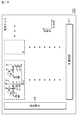
- FIG. 1 is a schematic perspective view illustrating a configuration example of a solid-state imaging device according to an embodiment of the present disclosure.
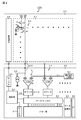
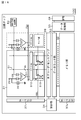
- FIG. 2 is a circuit diagram illustrating a specific configuration of the first chip side circuit and the second chip side circuit in the solid-state imaging device according to the first embodiment.
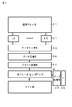
- FIG. 3 is a block diagram illustrating an example of a specific configuration of the signal processing unit in the solid-state imaging device according to the first embodiment.
- FIG. 4 is a timing chart for explaining the circuit operation of the solid-state imaging device according to the first embodiment.
- FIG. 5 is a circuit diagram showing an example of a circuit configuration for cutting off the current path between the signal line and the current source when the operation of the current source is stopped.
- FIG. 5 is a circuit diagram showing an example of a circuit configuration for cutting off the current path between the signal line and the current source when the operation of the current source is stopped.
- FIG. 6 is a block diagram for explaining the operation of storing data from the data latch unit to the memory unit and outputting the data from the memory unit.
- FIG. 7 is a block diagram illustrating another example of a specific configuration of the signal processing unit in the solid-state imaging device according to the first embodiment.
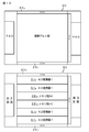
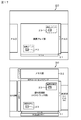
- FIG. 8 is a layout diagram showing a layout example of a laminated chip in the case of adopting a configuration in which two systems of AD converters and accompanying circuit portions are provided.
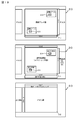
- FIG. 9 is a layout diagram showing a layout example 1 of the multilayer chip in the case of adopting a configuration in which four systems of AD converters and accompanying circuit portions are provided.
- FIG. 10 is a layout diagram showing a layout example 2 of the laminated chip in the case of adopting a configuration in which four systems of AD converters and accompanying circuit portions are provided.
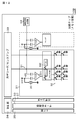
- FIG. 11 is a circuit diagram illustrating a specific configuration of a circuit on the first chip side in the solid-state imaging device according to the second embodiment.
- FIG. 12 is a circuit diagram illustrating a specific configuration of a circuit on the second chip side in the solid-state imaging device according to the second embodiment.
- FIG. 13 is a timing chart for explaining the circuit operation of the solid-state imaging device according to the second embodiment.
- FIG. 14 is a layout diagram illustrating a layout example of the multilayer chip in the solid-state imaging device according to the second embodiment.
- FIG. 15 is a circuit diagram illustrating a specific configuration of a circuit on the first chip side in the solid-state imaging device according to the third embodiment.
- FIG. 16 is a circuit diagram illustrating a specific configuration of a circuit on the second chip side in the solid-state imaging device according to the third embodiment.
- FIG. 17 is a layout diagram showing an example of the layout of the multilayer chip in the solid-state imaging device according to the third embodiment.
- FIG. 18 is a layout diagram illustrating another example of the layout of the laminated chips in the solid-state imaging device according to the third embodiment.
- FIG. 19 is a block diagram illustrating a configuration example of an imaging apparatus that is an example of the electronic apparatus of the present disclosure.
- the solid-state imaging device includes a signal processing unit, a memory unit, a data processing unit, and a control unit in addition to the pixel array unit.
- the pixel array section includes unit pixels including photoelectric conversion elements (hereinafter sometimes simply referred to as “pixels”) two-dimensionally arranged in a matrix (matrix). That is, the solid-state imaging device of the present disclosure is an XY address type solid-state device that can read out pixel signals in units of one pixel, a plurality of pixels, or one or a plurality of rows (lines).
- a CMOS image sensor can be exemplified as a typical XY address type solid-state imaging device.
- a control line (row control line) is wired for each pixel row and a signal line (column signal line / vertical signal line) is wired for each pixel column with respect to the matrix pixel array.
- a current source may be connected to each of the signal lines.
- a signal (analog pixel signal) is read from each pixel of the pixel array portion with respect to this signal line. This reading can be performed, for example, under a rolling shutter that performs exposure in units of one pixel or one line (one row). This readout under the rolling shutter may be referred to as rolling readout.
- the signal processing unit includes an AD (analog-digital) converter that digitizes an analog pixel signal read from each pixel of the pixel array unit to the signal line, and converts the AD-converted image data into a frame rate (1 second).
- the number of images that can be captured per hit) can be transferred to the memory unit at a faster speed (first speed). As described above, by transferring the pixel data to the memory unit at a first speed faster than the frame rate (high-speed transfer), high-speed reading faster than the frame rate can be realized.
- the memory unit is not particularly limited.
- the memory unit may be a non-volatile memory or a volatile memory.
- the data processing unit may be configured to read pixel data from the memory unit at a first speed, that is, a speed (second speed) slower than the transfer speed of the signal processing unit.
- a speed (second speed) slower than the transfer speed of the signal processing unit e.g., a speed (second speed) slower than the transfer speed of the signal processing unit.
- the pixel data while stopping the operation of the current source connected to each of the signal lines and the operation of at least the AD converter of the signal processing unit can be configured to perform intermittent driving.
- intermittent driving that stops the operation of the current source and the operation of the AD converter when reading out the pixel data from the memory unit, power is consumed by the amount originally consumed by the current source and the AD converter during the stop period. Therefore, further reduction in power consumption can be achieved.
- a solid-state imaging device capable of performing high-speed reading of pixel data with lower power consumption can be realized.
- a solid-state imaging device that is, the solid-state imaging device of the present disclosure is used for imaging in an electronic device such as a mobile terminal device, a digital still camera, a single-lens reflex camera, a camcorder, or a surveillance camera having an imaging function such as a mobile phone.
- Part image capturing part
- the driving method thereof, and the electronic apparatus when the pixel data is read from the memory unit, the operation of the current source and the operation of the AD converter are stopped. It can be configured to stop in units of vertical synchronization signals. “Stopping in units of vertical synchronization signals” also means “stopping in synchronization with vertical synchronization signals”.
- the pixel array unit includes the signal processing unit, the memory unit, the data processing unit, and the control unit.
- the chip may be formed on at least one chip different from the formed chip, and may have a structure in which the chip in which the pixel array portion is formed and at least one other chip are stacked (so-called stacked structure).
- the control unit can be configured to control the circuit on the chip side in which the pixel array unit is formed and at least one other circuit on the chip side in synchronization.
- the signal processing unit is configured to output the analog pixel signal read from the pixels of the pixel array unit for each pixel row.
- the signal processing can be performed in parallel (column parallel) in units of pixel columns.
- the signal processing unit may include a data latch unit and a parallel-serial conversion unit, and the pixel data digitized by the AD converter may be pipeline-transferred to the memory unit.
- the data latch unit latches the pixel data digitized by the AD converter.
- the parallel-serial conversion unit converts the pixel data output from the data latch unit from parallel data to serial data.
- the signal processing unit may include a data latch unit, a data compression unit, and a parallel-serial conversion unit, and the pixel data digitized by the AD converter may be pipeline-transferred to the memory unit. it can. At this time, it is preferable to perform digitization processing by an AD converter within one horizontal period, and transfer the digitized pixel data to the data latch unit within the next one horizontal period.
- the data compression unit compresses the pixel data output from the data latch unit.
- the parallel-serial conversion unit converts the pixel data output from the data compression unit from parallel data to serial data.
- the signal processing unit includes two or more AD converters, and the two or more AD conversions are performed.
- the digital signal processing can be performed in parallel in the device. At this time, it is preferable to arrange two or more AD converters separately on both sides of the extension direction of the signal lines of the pixel array section.
- the solid-state imaging device of the present disclosure including the preferable configuration described above, a driving method thereof, and an electronic device, a predetermined number of current sources, signal processing units, and memory units connected to the signal lines are provided. It is possible to adopt a configuration in which each pixel is used as a unit and provided for each unit. At this time, the signal processing unit performs signal processing in parallel (pixel parallel) in units of pixel signals read out for each unit of a predetermined number of pixels from each pixel of the pixel array unit. The signal processing may be performed in a predetermined order for a plurality of pixels.
- a decoder that specifies a column address for the memory unit;
- a sense amplifier that reads pixel data at a specified address can be used. At that time, pixel data can be read from the memory portion through the sense amplifier and the decoder.
- the data processing unit is configured to read pixel data from the memory unit during the exposure period. be able to.
- the current source connected to the signal line is stopped in units of the vertical synchronization signal for the control unit.
- the current path between the signal line and the current source can be cut.
- FIG. 1 is a schematic perspective view illustrating a configuration example of the solid-state imaging device according to the first embodiment of the present disclosure.
- CMOS image sensor case of a CMOS image sensor will be described as an example of the solid-state imaging device according to the first embodiment.
- the present invention is not limited to application to a CMOS image sensor.
- the solid-state imaging device 10A includes a first chip (semiconductor substrate) 20 and a second chip 30, and the first chip 20 is an upper chip, and the second chip.
- 30 is stacked as a lower chip (so-called stacked structure).
- the upper first chip 20 is a pixel chip in which a pixel array unit (pixel unit) 21 in which unit pixels 40 including photoelectric conversion elements are two-dimensionally arranged in a matrix is formed.
- the peripheral portion of the first chip 20 is provided with pad portions 22 1 and 22 2 for electrical connection with the outside, and vias (VIA) for electrical connection with the second chip 30. ) 23 1 and vias 23 2 are provided.
- the pad portion 22 1 and the pad portion 22 2 are provided on both the left and right sides of the pixel array portion 21, but a configuration provided on one side of the left and right is also possible.
- the via 23 1 and the via 23 2 are provided on both upper and lower sides with the pixel array portion 21 in between, a configuration provided on one of the upper and lower sides may be employed.
- a pad portion is provided in the lower second chip 30 to open the first chip 20 and bonding to the pad on the second chip 30 side, or substrate mounting from the second chip 30 by TSV (Through silicon via) It is also possible to adopt a configuration to do so.
- the pixel signal obtained from each pixel 40 of the pixel array unit 21 is an analog signal, and this analog pixel signal is transmitted from the first chip 20 to the second chip 30 through the vias 23 1 and 23 2. Become.
- the lower second chip 30 includes a signal processing unit 31, a memory unit 32, data processing, as well as a driving unit (not shown) that drives each pixel 40 of the pixel array unit 21 formed on the first chip 20.
- This is a circuit chip in which peripheral circuit parts such as the part 33 and the control part 34 are formed.
- the signal processing unit 31 performs predetermined signal processing including digitization (AD conversion) on the analog pixel signal read from each pixel 40 of the pixel array unit 21.
- the memory unit 32 stores pixel data that has been subjected to predetermined signal processing by the signal processing unit 31.
- the data processing unit 33 reads out pixel data stored in the memory 32 in a predetermined order, and performs a process of outputting the data outside the chip.
- the control unit 34 for example, based on the reference signals such as the horizontal synchronization signal XHS, the vertical synchronization signal XVS, and the master clock MCK given from the outside of the chip, the driving unit, the signal processing unit 31, the memory unit 32, and The operation of the peripheral circuit unit of the data processing unit 33 is controlled. At this time, the control unit 34 synchronizes the circuit on the first chip 20 side (pixel array unit 21) and the circuit on the second chip 30 side (signal processing unit 31, memory unit 32, and data processing unit 33). It will be controlled while taking.
- the solid-state imaging device 10A formed by laminating the first chip 20 and the second chip 30 only needs to have a size (area) enough to form the pixel array unit 31 as the first chip 20.
- the size (area) of the first chip 20 and thus the size of the entire chip can be reduced.
- the process can be optimized in manufacturing the solid-state imaging device 10A. There is also an advantage that can be achieved.
- an analog pixel signal is transmitted from the first chip 20 side to the second chip 30 side, while a circuit portion that performs analog / digital processing is configured in the same substrate (second chip 30), and the first chip 20 side.
- High-speed processing can be realized by a configuration in which the circuit of the second chip 30 and the circuit on the second chip 30 side are controlled in synchronization.
- a clock delay occurs due to the influence of parasitic capacitance and the like, which hinders high-speed processing.
- FIG. 2 is a circuit diagram illustrating a specific configuration of the circuit on the first chip 20 side and the circuit on the second chip 30 side in the solid-state imaging device 10A according to the first embodiment. As described above, electrical connection between the circuit on the first chip 20 side and the circuit on the second chip 30 side is performed via the vias (VIA) 23 1 and 23 2 shown in FIG. .
- each pixel 40 of the pixel array unit 21 is arranged based on an address signal given from the second chip 30 side.
- a row selection unit 25 for selecting in units of rows is provided.
- the row selection unit 25 is provided on the first chip 20 side, but a configuration provided on the second chip 30 side is also possible.
- the unit pixel 40 has, for example, a photodiode 41 as a photoelectric conversion element.
- the unit pixel 40 includes four transistors, for example, a transfer transistor (transfer gate) 42, a reset transistor 43, an amplification transistor 44, and a selection transistor 45.
- N-channel transistors are used as the four transistors 42 to 45.
- the conductivity type combinations of the transfer transistor 42, the reset transistor 43, the amplification transistor 44, and the selection transistor 45 illustrated here are merely examples, and are not limited to these combinations. That is, a combination using a P-channel transistor can be used as necessary.
- a transfer signal TRG, a reset signal RST, and a selection signal SEL which are drive signals for driving the pixel 40, are appropriately supplied from the row selection unit 25 to the unit pixel 40. That is, the transfer signal TRG is applied to the gate electrode of the transfer transistor 42, the reset signal RST is applied to the gate electrode of the reset transistor 43, and the selection signal SEL is applied to the gate electrode of the selection transistor 45.
- the photodiode 41 has an anode electrode connected to a low potential power source (for example, ground), and photoelectrically converts received light (incident light) into photocharge (here, photoelectrons) having a charge amount corresponding to the amount of light. Then, the photocharge is accumulated.
- the cathode electrode of the photodiode 41 is electrically connected to the gate electrode of the amplification transistor 44 through the transfer transistor 42.
- a node 46 electrically connected to the gate electrode of the amplification transistor 44 is called an FD (floating diffusion / floating diffusion region) part.
- the transfer transistor 42 is connected between the cathode electrode of the photodiode 41 and the FD portion 46.
- a transfer signal TRG whose high level (for example, V DD level) is active (hereinafter referred to as “High active”) is supplied from the row selection unit 25 to the gate electrode of the transfer transistor 42.
- the transfer transistor 42 becomes conductive, and the photoelectric charge photoelectrically converted by the photodiode 41 is transferred to the FD unit 46.
- the reset transistor 43 has a drain electrode connected to the pixel power source V DD and a source electrode connected to the FD unit 46.
- a high active reset signal RST is supplied from the row selection unit 25 to the gate electrode of the reset transistor 43.
- the reset transistor 43 becomes conductive, and the FD unit 46 is reset by discarding the charge of the FD unit 46 to the pixel power source V DD .
- the amplification transistor 44 has a gate electrode connected to the FD portion 46 and a drain electrode connected to the pixel power source VDD . Then, the amplification transistor 44 outputs the potential of the FD unit 46 after being reset by the reset transistor 43 as a reset signal (reset level) V reset . Further, the amplification transistor 44 outputs the potential of the FD section 46 after the signal charge is transferred by the transfer transistor 42 as a light accumulation signal (signal level) V sig .
- the selection transistor 45 has a drain electrode connected to the source electrode of the amplification transistor 44 and a source electrode connected to the signal line 26.
- a high active selection signal SEL is supplied from the row selection unit 25 to the gate electrode of the selection transistor 45.
- the selection transistor 45 is turned on, and the unit pixel 40 is selected and the signal output from the amplification transistor 44 is read out to the signal line 26.
- the reset potential of the FD section 46 is set as the reset level V reset , and then the potential of the FD section 46 after the transfer of the signal charge is set as the signal level V sig in order. It is read out to the signal line 26.
- the signal level V sig includes a component of the reset level V reset .
- the selection transistor 45 is configured to be connected between the source electrode of the amplification transistor 44 and the signal line 26, but the circuit is connected between the pixel power supply V DD and the drain electrode of the amplification transistor 44. It is also possible to adopt a configuration.
- the unit pixel 40 is not limited to the pixel configuration composed of the above four transistors.
- the configuration of the pixel circuit There is no limitation on the configuration of the pixel circuit.
- circuit configuration on the second chip side Next, the circuit configuration on the second chip 30 side will be described with reference to FIG.
- a current source 35, a decoder 36, a row decoder 37, and an interface (IF) A part 38 and the like are provided.
- the current source 35 is connected to each signal line 26 from which a signal is read from each pixel 40 of the pixel array unit 21 for each pixel column.
- the current source 35 has, for example, a so-called load MOS circuit configuration including a MOS transistor whose gate potential is biased to a constant potential so as to supply a certain current to the signal line 26.
- the current source 35 including the load MOS circuit supplies the constant current to the amplification transistor 44 of the unit pixel 40 in the selected row, thereby operating the amplification transistor 44 as a source follower.
- the decoder 36 When the decoder 36 selects each pixel 40 of the pixel array unit 31 in units of rows under the control of the control unit 34, the decoder 36 gives an address signal for designating the address of the selected row to the row selection unit 25.
- the row decoder 37 designates a row address when writing pixel data to the memory unit 32 or reading pixel data from the memory unit 32 under the control of the control unit 34.
- the signal processing unit 31 includes at least an AD converter 51 that digitizes (AD converts) an analog pixel signal read from each pixel 40 of the pixel array unit 21 through the signal line 26, and a pixel for the analog pixel signal.
- the signal processing (column parallel AD) is performed in parallel in units of columns.
- the signal processing unit 31 further includes a reference voltage generation unit 52 that generates a reference voltage used when AD conversion is performed by the AD converter 51.
- the reference voltage generation unit 52 generates a reference voltage having a so-called ramp (RAMP) waveform (gradient waveform) in which the voltage value changes stepwise as time passes.
- RAMP ramp waveform
- the reference voltage generation unit 52 can be configured using, for example, a DAC (digital-analog conversion) circuit.
- the AD converter 51 is provided for each pixel column of the pixel array unit 21, that is, for each signal line 26, for example. That is, the AD converter 51 is a so-called column-parallel AD converter that is arranged by the number of pixel columns of the pixel array unit 21. Then, the AD converter 51 generates a pulse signal having a magnitude (pulse width) in the time axis direction corresponding to the magnitude of the level of the pixel signal, for example, and sets the length of the pulse width period of the pulse signal. The AD conversion process is performed by measuring.
- the AD converter 51 has at least a comparator (COMP) 511 and a counter 512.
- the comparator 511 receives the analog pixel signal (the signal level V sig and the reset level V reset described above) read from each pixel 40 of the pixel array unit 21 through the signal line 26 as a comparison input, and is supplied from the reference voltage generation unit 52.
- the reference voltage Vref of the ramp wave is used as a standard input, and both inputs are compared.
- the comparator 511 outputs, for example, when the reference voltage V ref is larger than the pixel signal, the output is in the first state (for example, high level), and when the reference voltage V ref is equal to or lower than the pixel signal, the output is output.
- a second state eg, low level
- the output signal from the comparator 511 is a pulse signal having a pulse width corresponding to the level of the pixel signal.
- an up / down counter is used as the counter 512.
- the counter 512 is supplied with the clock CK at the same timing as the supply start timing of the reference voltage V ref to the comparator 511.
- the counter 512 which is an up / down counter performs a down (DOWN) count or an up (UP) count in synchronization with the clock CK, so that the period of the pulse width of the output pulse of the comparator 511, that is, the comparison operation
- the comparison period from the start to the end of the comparison operation is measured.
- the counter 512 counts down the reset level V reset and the signal level V sig sequentially read from the unit pixel 40 with respect to the reset level V reset and increases with respect to the signal level V sig . Count.
- the AD converter 51 performs a CDS (Correlated Double Sampling) process in addition to the AD conversion process.
- CDS Correlated Double Sampling
- the “CDS processing” removes the fixed pattern noise unique to the pixel such as reset noise of the unit pixel 40 and threshold variation of the amplification transistor 44 by taking the difference between the signal level V sig and the reset level V reset. It is processing to do.
- the count result (count value) of the counter 512 becomes a digital value obtained by digitizing the analog pixel signal.
- FIG. 3 is a block diagram illustrating an example of a specific configuration of the signal processing unit 31 in the solid-state imaging device 10A according to the first embodiment.
- the signal processing unit 31 includes a data latch unit 53 and a parallel-serial (hereinafter abbreviated as “parasiri”) conversion unit 54 in addition to the AD converter 51, and is digitized by the AD converter 51.
- the pipeline data is transferred to the memory unit 32 by pipeline.
- the signal processing unit 31 performs digitization processing by the AD converter 51 within one horizontal period, and performs processing of transferring the digitized pixel data to the data latch unit 53 within the next one horizontal period.
- the memory unit 32 is provided with a column decoder / sense amplifier 39 as its peripheral circuit.
- the row decoder 37 (see FIG. 2) described above designates a row address for the memory unit 32, whereas the column decoder designates a column address for the memory unit 32.
- the sense amplifier amplifies the weak voltage read from the memory unit 32 through the bit line to a level that can be handled as a digital level.
- the pixel data read through the column decoder / sense amplifier 39 is output to the outside of the second chip 30 via the data processing unit 33 and the interface unit 38.
- the two or more AD converters 51 are arranged separately in the extending direction of the signal line 26 of the pixel array unit 21, that is, on both the upper and lower sides of the pixel array unit 21.
- two (two systems) of data latch units 53, parallel-serial conversion units 54, memory units 32, and the like are also provided.
- a solid-state imaging device having a configuration in which, for example, two systems of AD converters 51 are provided
- row scanning is performed in units of two pixel rows. Then, the signal of each pixel in one pixel row is read out on one side in the vertical direction of the pixel array unit 21, and the signal of each pixel in the other pixel row is read out on the other side in the vertical direction of the pixel array unit 21, respectively.
- Digitization processing is performed in parallel by the two AD converters 51. Subsequent signal processing is also performed in parallel. As a result, pixel data can be read at a higher speed than when row scanning is performed in units of one pixel row.
- pixel signals from the pixels 40 of the pixel array unit 21 on the first chip 20 side are read at a reading speed faster than the frame rate, for example, 240 [fps] by rolling reading performed under a rolling shutter. Reads at high speed.
- the analog pixel signal read by the rolling readout is transmitted from the first chip 20 to the signal processing unit 31 on the second chip 30 side via vias (VIA) 23 1 and 23 2 .
- the analog pixel signal is digitized by the AD converter 51.
- the pixel data digitized by the AD converter 51 is pipeline-transferred to the memory unit 32 and stored in the memory unit 32.
- the signal processing unit 31 performs digitization processing by the AD converter 51 within one horizontal period, and performs pipeline transfer to the memory unit 32 within the next one horizontal period.
- the speed at which the digitized pixel data is transferred to the memory unit 32 is a reading speed by rolling reading, that is, 240 [fps]. Accordingly, the signal processing unit 31 transfers the pixel data digitized by the AD converter 51 to the memory unit 32 at a speed (first speed) faster than the frame rate.
- the pixel signal is read out from each of the unit pixels 40 by high-speed reading faster than the frame rate, and the digitized pixel data is read out at a first speed faster than the frame rate. 32 is transferred at high speed and stored.
- the pixel data stored in the memory unit 32 is read by the data processing unit 33 via the column decoder / sense amplifier 39 at a second speed that is slower than the first speed, for example, 80 [fps].
- the data is output to the outside of the second chip 30 via the interface unit 38.
- reading of the pixel data from the memory unit 32 is performed during the exposure period.
- the conventional technique described in Patent Document 1 employs a configuration in which the pixel data is stored in the memory unit, and then enters a standby state, and then photographing is started, so that real-time image photographing cannot be performed.
- the present embodiment employs a configuration in which pixel data is read from the memory unit 32 during the exposure period, so that pixel data of moving images and still images can be read in real time.
- the memory unit 32 various types of memories can be used regardless of whether they are nonvolatile or volatile.
- the volatile memory for example, DRAM
- the volatile memory can be reduced to 50 [msec] by performing the process from the start of writing pixel data to the memory unit 32 to the completion of reading of the pixel data by the data processing unit 33 at a speed of 20 [fps] or more. It is also possible to eliminate the refresh operation requiring a degree.
- AD conversion and data output are performed by pipeline transfer of about several [ ⁇ sec].
- the writing speed of DRAM is equal or less, that is, several [ ⁇ sec] or less. Therefore, with the pipeline configuration as shown in FIG. 3, it is possible to perform from pixel signal reading to pixel data writing in the memory unit 32.
- the AD converter 51 performs digitization processing within one horizontal period (XHS), transfers the digital data to the data latch unit 53 within the next one horizontal period, and the data latch unit 53 Save to. Thereafter, the parallel-serial conversion unit 54 converts the parallel signal into a serial signal, and writes the pixel data into the memory unit 32 under the designation of the row address by the row decoder 37 and the designation of the column address by the column decoder of the column decoder / sense amplifier 39. . In other words, the pixel data is AD converted in parallel by the AD converter 51, latched in the data latch unit 53, and then written in the memory unit 32 in parallel to realize pipeline transfer.
- XHS horizontal period
- the parallel-serial conversion unit 54 converts the parallel signal into a serial signal, and writes the pixel data into the memory unit 32 under the designation of the row address by the row decoder 37 and the designation of the column address by the column decoder of the column decoder / sense amplifier 39.
- the pixel data is AD converted in parallel by the
- the data latch unit 53 stores the memory write and the next row of digital data in the next horizontal period.
- a method of pipeline transfer stored in the data latch unit 53 can also be adopted.
- the operation of the current source 35 connected to each of the signal lines 26 and at least the AD converter of the signal processing unit 31 are used.
- the operation of 51 is stopped in units of the vertical synchronization signal XVS.
- “when reading out pixel data from the memory unit 32” can be said to be after the pixel data is stored in the memory unit 32 at high speed by pipeline transfer, or during the exposure period.
- the power supply design is facilitated by stopping the circuit operation in synchronization with the vertical synchronization signal XVS (in units of the vertical synchronization signal XVS) without depending on the exposure period.
- the operation of the current source 35 and the stop of the operation of at least the AD converter 51 of the signal processing unit 31 are executed under the control of the control unit 34.
- exposure is started by resetting the unit pixel 40 (shutter operation) after 240 [fps] high-speed rolling readout. It is possible to stop the operations of the current source 35 and the AD converter 51 during the exposure period. Therefore, by stopping each operation of the current source 35 and the AD converter 51 for a period from the start of reading pixel data from the memory unit 32 of the current frame to the start of reading pixel signals from the unit pixel 40 of the next frame, The power consumption can be reduced by the amount originally consumed by the current source 35 and the AD converter 51 during the stop period.
- the operation of the current source 35 can be stopped by cutting (cutting) the current path between the signal line 26 and the current source 35 under the control of the control unit 34. More specifically, for example, as shown in FIG. 5, by inserting the transistors Q 1 between the signal line 26 and the current source 35 to the transistor Q 1 in a non-conducting state by a low level control signal, The operation of the current source 35 can be stopped.
- a fixed potential may be applied to the signal line 26. More specifically, for example, as shown in FIG. 5, connects the transistor Q 2 between the signal line 26 and a fixed potential, the transistor Q 2, conducted by the inverted control signal of the control signal through the inverter INV By setting the state, a fixed potential can be applied to the signal line 26.
- the fixed potential is applied to the signal line 26 in order to eliminate the influence on the FD portion 46 of the unit pixel 40 due to the signal line 26 being in a floating state. is there. That is, when the signal line 26 is in a floating state, for example, when the potential of the signal line 26 fluctuates, the fluctuation of the potential may cause the potential of the FD portion 46 to fluctuate due to coupling due to the parasitic capacitance of the amplification transistor 44. In order to eliminate such an influence on the FD section 46, a fixed potential is applied to the signal line 26.
- the shutter operation may span the first vertical period (1XVS) and the next vertical period (2XVS). In such a case, it may be controlled to stop the operation of the current source 35 after the shutter operation.
- the influence of the standby operation of the current source 35 that is, the fluctuation of the power supply potential and the fluctuation of the potential of the signal line 26 can be prevented. If the shutter start is after the next vertical period (2XVS), there is no influence of the standby operation of the current source 35.
- the AD converter 31 and accompanying circuit portions that is, two circuit portions such as the data latch portions 53 (53 1 , 53 2 ) and the memory portions 32 (32 1 , 32 2 ) are provided.
- An example is given. However, basically the same can be said for one system.
- the pixel data after AD conversion is latched in the data latch unit 53.
- the parallel-serial conversion unit 54 caches 16 kbits in the column decoder in units of 128, for example.
- data is stored in the memory unit 32 using a sense amplifier.
- the memory unit 32 has a four-bank configuration, but this is only an example, and the number of banks should be determined so that image data can be stored in units of horizontal pixels.
- a pipeline configuration is employed in which data is written to the bits of each memory unit in parallel with the rolling read, so that data storage from the data latch unit 53 to the memory unit 32 is completed in one vertical period. Can do. After completion of data writing to the memory unit 32, the operations of the current source 35 and the AD converter 51 are stopped as described above, and reading of data from the memory unit 32 is started.
- the data is rearranged by the multiplexer 55 (55 1 , 55 2 ) and the data processing unit 33.
- the data is output from the interface unit 38 while being synthesized.
- power consumption can be reduced by a method such as fixing the output of the interface unit 38. Specifically, for example, the power consumption can be reduced by stopping the clock supplied to the output unit of the interface unit 38.
- FIG. 7 is a block diagram illustrating another example of a specific configuration of the signal processing unit in the solid-state imaging device according to the first embodiment.
- the signal processing unit 31 includes a data compression unit 56 in addition to the AD converter 51, the data latch unit 53, and the parallel-serial conversion unit 54, and the pixel data digitized by the AD converter 51 is processed. It has a pipeline configuration for pipeline transfer to the memory unit 32. At that time, the signal processing unit 31 performs digitization processing by the AD converter 51 within one horizontal period, and transfers the digitized pixel data to the data latch unit 53 within the next one horizontal period.
- the data compression unit 56 is provided, for example, between the data latch unit 53 and the parallel-serial conversion unit 54, compresses the pixel data output from the data latch unit 53, and supplies the compressed pixel data to the parallel-serial conversion unit 54.
- a compression method of the data compression unit 56 for example, DPCM (differential pulse-code modulation) can be exemplified.
- the data compression unit 56 is provided between the data latch unit 53 and the memory unit 32, and the data compression unit 56 compresses the data before storing the data in the memory unit 32, thereby reducing the memory capacity of the memory unit 32. Can be reduced. And by reducing the capacity of the memory unit 32, the layout area of the second chip 30 on which the signal processing unit 31 is mounted can be reduced.
- Multilayer chip layout As described above, a multilayer chip in the case of adopting a configuration in which a plurality of systems, for example, two systems, are provided for the AD converter 51 and the circuit portions associated therewith, and the signals of the respective pixels in the two pixel rows are processed in parallel. That is, consider the layout of a chip formed by stacking the first chip 20 and the second chip 30.
- the first chip 20 in which the pixel array unit 21 is formed, the signal processing unit 31 including the AD converter 51, the memory unit 32, the data processing unit 33, and the control unit 34 are provided.
- a configuration of a laminated chip formed by laminating the formed second chip 30 is adopted.
- the AD converters 51 1 and 51 2 are arranged on both the upper and lower sides of the second chip 30 (which can be said to be the upper and lower sides of the pixel array unit 21).
- the memory units 32 1 and 32 2 can be arranged adjacent to each other between 1 and 51 2 .
- the control unit 34 is provided in an empty area such as between the memory unit 32 1 and the memory unit 32 2 .
- FIG. 9 is a layout diagram showing a layout example 1 of the multilayer chip in the case of adopting a configuration in which four systems of AD converters 51 and accompanying circuit portions are provided.
- two vias (VIA) are provided in the central portion of the pixel array unit 21 in the vertical direction, and the signals of each pixel in the four pixel rows are sent to the two vias on the upper and lower sides of the pixel array unit 21.
- Data is simultaneously read out to the second chip 30 side through 23 1 , 23 2 and two systems of vias 23 3 , 23 4 at the center.
- AD converters 51 1 to 51 4 are arranged in the vicinity of each of the vias 23 1 to 23 4 . Further, it arranged memory unit 32 1, 32 3 between the AD converter 51 1 and AD converter 51 3, the memory unit 32 2 between the AD converter 51 2 and AD converter 51 4, 32 4 Are arranged adjacent to each other. As described above, even when the AD converter 51 and the accompanying circuit portions are provided in four systems, the memory units 32 1 and 32 3 and the memory units 32 2 and 32 4 can be arranged adjacent to each other. As a result, even in this layout example 1, the same operation and effect as in the layout example of FIG. 8 can be obtained.
- FIG. 10 is a layout diagram showing a layout example 2 of the laminated chip in the case of adopting a configuration in which four systems of AD converters 51 and accompanying circuit portions are provided.
- the second layout example similarly to the layout example of FIG. 8, two systems of vias 23 1 and 23 2 are provided on both upper and lower sides of the pixel array unit 21.
- two AD converters 51 1 in the vicinity of one of the vias 23 1, 51 3 are positioned adjacent, 2 other via 23 2 two AD converters in the vicinity of 51 , 51 4 are disposed adjacent.
- a memory unit 32 13 corresponding to the AD converters 51 1 and 51 3 and a memory unit 32 24 corresponding to the AD converters 51 2 and 51 4 and Are arranged adjacent to each other.
- a memory unit 32 13 and the memory unit 32 24 can be placed adjacent.
- the number of channels of the interface unit 38 can be reduced and the signal processing block (for example, the processing speed of DSP) can be reduced. This can contribute to lower power consumption of the entire system including the signal processing block at the subsequent stage.
- first chip 20 and the second chip 30 are connected to each other as a stacked chip, and the circuit on the first chip 20 side and the circuit on the second chip 30 side are synchronized under the control of the control unit 34.
- the control unit 34 As a result, since the data after AD change can be pipeline-transferred to the memory unit 32, synchronous design is facilitated.
- pixel data is read from the memory unit 32 during the exposure period, the pixel data is stored in the memory unit, and then enters a standby state. In addition, pixel data of moving images and still images can be read out. Therefore, real-time imaging is possible.
- the data compression unit 56 when the data compression unit 56 is provided between the data latch unit 53 and the memory unit 32 and the data compression unit 56 compresses the data and then stores the data in the memory unit 32, Since the memory capacity can be reduced, the layout area of the second chip 30 can be reduced.
- rolling distortion can be further improved by providing two or more AD converters 51 and accompanying circuit portions and pipeline-transferring the data after AD conversion to the memory unit 32.
- Solid-State Imaging Device According to Second Embodiment> Subsequently, a solid-state imaging device according to the second embodiment of the present disclosure will be described.
- the case of a CMOS image sensor will be described as an example of the solid-state imaging device according to the second embodiment.
- the present invention is not limited to application to a CMOS image sensor.
- the solid-state imaging device according to the second embodiment has a stacked structure in which the first chip 20 and the second chip 30 are stacked.
- a pixel array unit (pixel unit) 21 is formed on the first chip 20 side, and a signal processing unit 31 including an AD converter 51 on the second chip 30 side, a memory unit 32, a data processing unit 33, and a control unit.
- the circuit portion such as 34 is formed.
- FIG. 11 is a circuit diagram illustrating a specific configuration of a circuit on the first chip side in the solid-state imaging device according to the second embodiment
- FIG. 12 illustrates the second chip side in the solid-state imaging device according to the second embodiment. It is a circuit diagram which shows the specific structure of this circuit.
- the solid-state imaging device 10B sets a predetermined number of pixels 40 of the pixel array unit 21 as a group (unit), reads pixel signals from each pixel 40 for each group, and reads the read pixel signals as group units. Therefore, the signal processing including AD conversion is performed in parallel. That is, the solid-state imaging device 10A according to the first embodiment is a column-parallel AD conversion system that performs AD conversion of pixel signals in units of pixel columns, whereas the solid-state imaging device 10B according to the second embodiment. Is a pixel parallel AD conversion method in which AD conversion is performed in parallel in units of groups of a predetermined number of pixels.
- a predetermined number of pixels are grouped (one unit)
- a plurality of adjacent pixels belonging to the same pixel row are set as one unit, or a plurality of adjacent pixels in the vertical and horizontal directions are set as one unit.
- the present invention is not limited to a configuration in which pixel signals are read out in units of groups with a plurality of pixels as one unit, and ultimately, a configuration in which pixel signals are read out in units of individual pixels may be employed.
- vias (VIA) 23 that connect the pixel array unit 21 on the first chip 20 side and the signal processing unit 31 on the second chip 30 side are required in units of groups or pixels.
- the vias 23 for electrical connection between the chips can be realized by a well-known inter-wiring junction technique.
- the pixel signals read out in units of groups or pixels are transmitted from the first chip 20 side to the second chip 30 side through vias 23 provided in group units or pixel units.
- a column selection unit 27 is provided on the first chip 20 side in addition to the pixel array unit 21 and the row selection unit 25 as shown in FIG. .
- the column selection unit 27 selects each pixel 40 of the pixel array unit 21 in group units (or pixel units) in the pixel column arrangement direction (row direction) based on the address signal given from the second chip 30 side.
- the configuration in which the row selection unit 25 and the column selection unit 27 are provided on the first chip 20 side is employed, but a configuration in which the row selection unit 25 and the column selection unit 27 are provided on the second chip 30 side may be employed.
- the unit pixel 40 is configured to include two selection transistors 45 and 47 in addition to the transfer transistor 42, the reset transistor 43, and the amplification transistor 44.
- the two selection transistors 45 and 47 are both connected in series to the amplification transistor 44.
- One selection transistor 45 is driven by a row selection signal VSEL provided from the row selection unit 25.
- the other selection transistor 47 is driven by a column selection signal HSEL provided from the column selection unit 27.
- circuit configuration on the second chip side Corresponding to the unit pixels 40 being grouped in units of a predetermined number, and vias 23 being provided for each group, signal lines connected to the vias 23 on the second chip 30 as shown in FIG. 26 is wired.
- a current source 35 is connected to the signal line 26, and an AD converter 51 and further a memory unit 32 are connected to the signal line 26.
- the signal processing unit 31 including the signal line 26, the current source 35, the AD converter 51, the memory unit 32, and the like is provided in units of groups each having a predetermined number of pixels.
- the memory unit 32 can be exemplified by a DRAM, but is not particularly limited. That is, as in the case of the first embodiment, the memory unit 32 may be a volatile memory or a non-volatile memory.
- AD conversion is performed during the horizontal period (XHS) and data is output.
- XHS horizontal period
- AD conversion processing it is necessary to increase the number of pixels to be subjected to AD conversion at the same time.
- AD conversion processing it is necessary to perform AD conversion processing not in column parallel but in pixel parallel (unit of plural pixels).
- the AD converter 51 can be stopped longer by that amount, so that the power consumption can be further reduced.
- the operation period of the AD converter 51 is It is possible to make it 1/10 or less of the data output period.
- each pixel 40 of the pixel array unit 21 For reading pixel signals at a reading speed of 960 [fps], for example, about each pixel 40 of the pixel array unit 21, about 250 pixels, for example, 16 ⁇ 16 pixels are set as one unit (group).
- the AD conversion time in the AD converter 51 is 4 [ ⁇ sec]
- a pixel signal of 250 pixels can be read out in a time of 1 [msec] or less.
- the numerical value illustrated here is an example, and is not limited to these numerical values.
- a pixel unit (group) having 16 ⁇ 16 pixels as one unit is selected by addressing using a row selection signal VSEL provided from the row selection unit 25 and a column selection signal HSEL provided from the column selection unit 27. Then, an analog converter signal read from one pixel in the pixel unit selected by the row selection signal VSEL and the column selection signal HSEL is AD converted by the AD converter 51.
- CDS processing is performed by down-counting with respect to the reset level V reset in the counter 512 and up-counting with respect to the signal level V sig .
- the pixel data after the CDS processing is written into the memory unit 32 under the designation of the row address by the row decoder 37 and the designation of the column address by the column decoder of the column decoder / sense amplifier 39.
- the row selection unit 25 and the column selection unit 27 perform selective scanning in units of pixel units (groups), while a plurality of pixels in the selected pixel unit are arranged in parallel in a predetermined order in units of pixel units. Pixel selective scanning is performed.
- An example of selection of a pixel in the pixel unit is selection by a raster scan method.
- the remaining pixels in the pixel unit are subjected to pixel selection and AD conversion by the raster scan method by the row selection signal VSEL and the column selection signal HSEL, and the pixel data after the CDS processing is stored in the memory unit 32.
- the data stored in the memory unit 32 can be output (read) at a low speed by reading through the column decoder / sense amplifier 39.
- the solid-state imaging device 10B according to the present embodiment employs the pixel parallel AD conversion method, the pixel signal readout speed can be increased. As a result, the AD converter 51 can be stopped for a longer period of time, so that lower power consumption can be achieved.
- FIG. 14 is a layout diagram illustrating a layout example of the multilayer chip in the solid-state imaging device 10B according to the second embodiment.
- the pixel array unit 21 has a two-dimensional array of pixel units (groups) each having a predetermined number of pixels as a unit, and a via 23 is formed for each pixel unit. It has been configured.
- the signal processing unit 31 includes a circuit unit (pixel AD unit in the drawing) including the AD converter 51 and the memory unit 32 corresponding to the pixel unit of the pixel array unit 21.
- the via 23 is formed corresponding to the pixel unit for each pixel AD unit.
- Solid-State Imaging Device According to Third Embodiment> Subsequently, a solid-state imaging device according to a third embodiment of the present disclosure will be described.
- the case of a CMOS image sensor will be described as an example of the solid-state imaging device according to the third embodiment.
- the present invention is not limited to application to a CMOS image sensor.
- the solid-state imaging device according to the third embodiment has a stacked structure in which the first chip 20 and the second chip 30 are stacked.
- a pixel array unit (pixel unit) 21 is formed on the first chip 20 side, and a signal processing unit 31 including an AD converter 51 on the second chip 30 side, a memory unit 32, a data processing unit 33, and a control unit.
- the circuit portion such as 34 is formed.
- FIG. 15 is a circuit diagram illustrating a specific configuration of the circuit on the first chip side in the solid-state imaging device according to the third embodiment
- FIG. 16 is the second chip side in the solid-state imaging device according to the third embodiment. It is a circuit diagram which shows the specific structure of this circuit.
- the solid-state imaging device 10C according to the present embodiment also adopts a pixel parallel AD conversion method, similarly to the solid-state imaging device 10B according to the second embodiment. That is, the solid-state imaging device 10C according to the present embodiment groups a predetermined number of pixels 40 of the pixel array unit 21 as a group, reads pixel signals from each pixel 40 for each group, and reads the read pixel signals in units of groups. The signal processing including AD conversion is performed in parallel.
- the solid-state imaging device 10C according to the present embodiment is different from the solid-state imaging device 10B according to the second embodiment in the following points. That is, the solid-state imaging device 10B according to the second embodiment employs a configuration in which the memory unit 32 is provided together with the AD converter 51 in the signal processing unit 31, that is, a configuration in which the AD converter 51 and the memory unit 32 are mounted together. ing. In contrast, the solid-state imaging device 10C according to the present embodiment employs a configuration in which the memory unit 32 is provided outside the signal processing unit 31.
- the grouping of unit pixels 40 in units of a predetermined number is the same as in the second embodiment.
- a plurality of adjacent pixels belonging to the same pixel row are set as one unit, or adjacent vertically and horizontally.
- a plurality of pixels may be set as one unit.
- the present invention is not limited to a configuration in which pixel signals are read out in units of groups with a plurality of pixels as one unit, and ultimately, a configuration in which pixel signals are read out in units of individual pixels may be employed.
- the via (VIA) 23 that connects the pixel array unit 21 on the first chip 20 side and the signal processing unit 31 on the second chip 30 side is required in units of groups or pixels.
- the vias 23 for electrical connection between the chips can be realized by a well-known inter-wiring junction technique.
- the pixel signals read out in units of groups or pixels are transmitted from the first chip 20 side to the second chip 30 side through vias 23 provided in group units or pixel units.
- the configuration on the first chip 20 side is basically the same as that of the second embodiment. That is, since the configuration of the pixel parallel AD conversion is adopted, each pixel of the pixel array unit 21 is provided on the first chip 20 side in addition to the pixel array unit 21 and the row selection unit 25 as shown in FIG. A column selection unit 27 that selects 40 in the row direction in units of groups (or pixels) is provided. In addition, about the row selection part 25 and the column selection part 27, it is also possible to take the structure provided in the 2nd chip
- circuit configuration on the second chip side Corresponding to the unit pixels 40 being grouped in units of a predetermined number and the vias 23 being provided for each group, the signal lines connected to the vias 23 on the second chip 30 as shown in FIG. 26 is wired. A current source 35 is connected to the signal line 26. Further, a signal processing unit 31 is provided for each signal line 26.
- the signal processing unit 31 has a configuration in which the AD converter 51 and the memory unit 32 are mixedly mounted in the second embodiment, whereas the memory unit 32 is not included in the present embodiment. ing. That is, in the present embodiment, a configuration in which the memory unit 32 is provided outside the signal processing unit 31 is employed.
- the AD converter 51 includes a comparator (COMP) 511, an Nbit (N is an integer of 2 or more) counter 512, and a latch unit 513.
- the latch unit 513 includes unit circuits (latch circuits) for N bits of the counter 512, and is AD-converted by the operations of the comparator 511 and the counter 512, and the counter 512 performs an up / down counting operation.
- the digital data (pixel data) for one pixel subjected to CDS is latched.
- a row decoder 37 1 for selecting the latch unit 513 in the signal processing unit 31 a row decoder 37 2 to select each cell in the memory unit 32 in units of rows are provided.
- the pixel signal is AD-converted by the AD converter 51, and CDS processing is performed by the up / down counting operation of the counter 512.
- the digital data obtained in this way is latched in the latch unit 513.
- the digital data latched in the latch section 513 by selecting the selection signal RSEL supplied from the row decoder 37 1, sequentially read by the sense amplifiers of the column decoder / sense amplifier 39. Thereafter, the pipeline operation is performed by simultaneously performing the operation of writing to the memory unit 32 via the data latch unit 53 on a plurality of pixels.
- pixel selection and AD conversion operations are performed by the raster scan method, and digital data after CDS processing by the counter 512 is transferred to the memory unit 32 via the latch unit 513 and the sense amplifier of the column decoder / sense amplifier 39.
- the writing operation is performed.
- unit circuits latch circuits
- unit circuits are arranged in units of several bits, which are smaller than N bits, and a selection signal is provided for each bit unit. After selection by RSEL, the data may be read by the sense amplifier of the column decoder / sense amplifier 39 and written to the memory unit 32. Thereby, a pixel unit with a smaller number of pixels can be formed, and the merit of increasing the reading speed can be obtained.
- the data stored in the memory unit 32 can be output (read) at a low speed by reading through the data latch unit 53 and the column decoder / sense amplifier 39.
- the pixel parallel AD conversion method is employed as in the solid-state imaging device 10B according to the second embodiment, so that the pixel signal readout speed can be increased. As a result, the AD converter 51 can be stopped for a longer period of time, so that lower power consumption can be achieved.
- FIG. 17 is a layout diagram showing an example of the layout of the laminated chips in the solid-state imaging device 10C according to the third embodiment.
- the first chip 20 has a pixel array unit 21 in which pixel units each having a predetermined number of pixels as one unit are two-dimensionally arranged in a matrix, and a via 23 is formed for each pixel unit.
- the second chip 30 is provided with a circuit unit (a pixel AD unit in the figure) including the AD converter 51 and the like corresponding to the pixel unit of the pixel array unit 21, and the pixel unit is provided for each pixel AD unit.
- a via 23 is formed, and a memory unit 32 is provided outside the formation region of the signal processing unit 31.
- FIG. 18 is a layout diagram showing another example of the layout of the laminated chips in the solid-state imaging device 10C according to the third embodiment.
- a two-layer stacked structure in which two chips of the first chip 20 and the second chip 30 are stacked is adopted, whereas in the layout example, the first chip 20 and the second chip 30 are used.
- a three-layer stacked structure in which three chips of the third chip 60 are stacked is stacked.
- the structure is not limited to a three-layer structure, and a four-layer structure or more is also possible.
- the pixel array unit 21 is arranged on the first chip 20, and the circuit unit (AD unit in the figure) including the AD converter 51 is arranged on the second chip 30.
- the memory unit 32 is arranged on the third chip 60, and the second chip 30 is laminated in the middle, for example.
- the order of stacking the first chip 20, the second chip 30, and the third chip 60 is arbitrary, but the second chip 30 on which the peripheral circuit including the control unit 35 is mounted should be in the middle. This is preferable because the first and third chips 20 and 60 to be controlled by the control unit 35 are located immediately above and immediately below the second chip 30.
- the memory unit 32 is provided in a third chip 60 other than the second chip 30 provided with the circuit unit including the AD converter 51 and the peripheral circuit including the control unit 35, that is, the third chip 60.
- the chip area can be reduced as compared with the layout example in which the memory section 32 is provided in the second chip 30.
- FIG. 17 and FIG. a configuration in which the second chip 30 on which a circuit unit including the AD converter 51 and the like is mounted and the third chip 60 on which the memory unit 32 and the like are mounted is connected by a via (VIA2). It is done.
- the vias (VIA1 / VIA2) for electrical connection between the chips can be realized by a well-known interconnecting technique.
- the pixel parallel AD conversion method can be used to increase the pixel signal readout speed. Therefore, the AD converter 51 can be stopped for a long time. Therefore, further reduction in power consumption can be achieved as compared with the solid-state imaging device 10A according to the first embodiment of the column parallel AD conversion method.
- the AD converter 51 and the memory unit 32 are not mixedly mounted in the signal processing unit 31 as in the solid-state imaging device 10B according to the second embodiment. 32 is provided outside the signal processing unit 31.
- the solid-state imaging device 10C according to the present embodiment can cope with a case where it is difficult to separate wells between an analog circuit such as a DRAM and the memory unit 32.
- the solid-state imaging device having the stacked structure since the pixel-parallel AD conversion method is used, the solid-state imaging device having the stacked structure has the pixel unit of the pixel array unit 21 and the signal processing. It can be said that it is preferable because a connection structure in which the pixel AD unit of the portion 31 is directly connected via the via 23 can be adopted.
- the solid-state imaging device to which the technology of the present disclosure is applied includes an imaging device such as a digital still camera and a video camera, a portable terminal device having an imaging function such as a mobile phone, a copying machine using a solid-state imaging device for an image reading unit, and the like It can be used as an imaging unit (image capturing unit) in all electronic devices.
- the above-described module form mounted on an electronic device, that is, a camera module is used as an imaging device.
- FIG. 19 is a block diagram illustrating a configuration example of an imaging apparatus (camera apparatus) that is an example of the electronic apparatus of the present disclosure.
- the imaging apparatus 100 includes an optical system including a lens group 101 and the like, an imaging element 102, a DSP circuit 103 that is a camera signal processing unit, a frame memory 104, a display device 105, a recording device 106, An operation system 107, a power supply system 108, and the like are included.
- the DSP circuit 103, the frame memory 104, the display device 105, the recording device 106, the operation system 107, and the power supply system 108 are connected to each other via a bus line 109.
- the lens group 101 takes in incident light (image light) from a subject and forms an image on the imaging surface of the imaging element 102.
- the imaging element 102 converts the amount of incident light imaged on the imaging surface by the lens group 101 into an electrical signal in units of pixels and outputs the electrical signal.
- the display device 105 includes a panel type display device such as a liquid crystal display device or an organic EL (electroluminescence) display device, and displays a moving image or a still image captured by the image sensor 102.
- the recording device 106 records a moving image or a still image captured by the image sensor 102 on a recording medium such as a memory card, a video tape, or a DVD (Digital Versatile Disk).
- the operation system 107 issues operation commands for various functions of the imaging apparatus 100 under the operation of the user.
- the power supply system 108 appropriately supplies various power supplies serving as operation power for the DSP circuit 103, the frame memory 104, the display device 105, the recording device 106, and the operation system 107 to these supply targets.
- Such an image pickup apparatus 100 is applied to a camera module for a mobile device such as a video camera, a digital still camera, and a mobile phone.
- the solid-state imaging apparatus according to each of the above-described embodiments that can realize high-speed reading of pixel data with lower power consumption can be used as the imaging element 102. This can greatly contribute to the reduction in power consumption of the imaging apparatus 100.
- a signal processing unit that includes an AD converter that digitizes an analog pixel signal read from each pixel of the pixel array unit to a signal line, and transfers the digitized pixel data at a first speed faster than the frame rate;
- a memory unit for holding pixel data transferred from the signal processing unit;
- a data processing unit that reads pixel data from the memory unit at a second speed slower than the first speed;
- a solid-state imaging device comprising: a control unit that performs control to stop operation of a current source connected to a signal line and at least operation of an AD converter of a signal processing unit when reading pixel data from a memory unit.
- the solid-state imaging device according to [1], wherein the control unit stops the operation of the current source and the operation of the AD converter in units of vertical synchronization signals.
- the signal processing unit, the memory unit, the data processing unit, and the control unit are formed on at least one chip different from the chip on which the pixel array unit is formed, The solid-state imaging device according to [1] or [2], wherein the chip in which the pixel array unit is formed and at least one other chip are stacked.
- a pixel array portion is formed on the first chip, A signal processing unit, a memory unit, a data processing unit, and a control unit are formed on the second chip, The solid-state imaging device according to the above [3], wherein the first chip and the second chip are stacked.
- a pixel array portion is formed on the first chip, A signal processing unit and a control unit are formed on the second chip, A memory unit and a data processing unit are formed on the third chip,
- the signal processing unit performs signal processing in parallel in units of pixel columns with respect to the analog pixel signal read from each pixel of the pixel array unit for each pixel row.
- a solid-state imaging device according to claim 1.
- the signal processing unit A data latch unit for latching pixel data digitized by the AD converter; A parallel-serial conversion unit that converts pixel data output from the data latch unit from parallel data to serial data;
- the solid-state imaging device according to [5], wherein the pixel data digitized by the AD converter is pipeline-transferred to the memory unit.
- the signal processing unit performs digitization processing by an AD converter within one horizontal period, and transfers the digitized pixel data to the data latch unit within the next one horizontal period. Imaging device.
- the signal processing unit performs digitization processing by the AD converter within one horizontal period, and transfers the digitized pixel data to the memory unit via the data latch unit and the column decoder within the next one horizontal period.
- the solid-state imaging device according to [6] above.
- the signal processing unit A data latch unit for latching pixel data digitized by the AD converter; A data compression unit for compressing pixel data output from the data latch unit; A parallel-serial conversion unit for converting pixel data output from the data compression unit from parallel data to serial data;
- the signal processing unit performs digitization processing by an AD converter within one horizontal period, and transfers the digitized pixel data to the data latch unit within the next one horizontal period.
- the signal processing unit performs digitization processing by an AD converter within one horizontal period, and converts the digitized pixel data into a data latch unit and a column decoder within the next one horizontal period.
- the signal processing unit includes two or more AD converters, and performs digital signal processing in parallel in the two or more AD converters according to any one of [5] to [9] The solid-state imaging device described.
- the solid-state imaging device according to [10], wherein the two or more AD converters are arranged separately on both sides of the extension direction of the signal line of the pixel array unit.
- the current source, the signal processing unit, and the memory unit connected to the signal line have a predetermined number of pixels as a unit, and are provided for each unit.
- the signal processing unit performs any one of the above-described [1] to [4], in which signal processing is performed in parallel on an analog pixel signal read in units of a predetermined number of pixels from each pixel of the pixel array unit.
- the solid-state imaging device according to [12], wherein the signal processing unit performs signal processing on the analog pixel signal read for each unit of the predetermined number of pixels in a predetermined order for a plurality of pixels in the unit.
- the data processing unit includes a decoder that specifies a column address for the memory unit, and a sense amplifier that reads pixel data of the specified address,
- the solid-state imaging device according to any one of [1] to [13], wherein pixel data is read from the memory unit through a sense amplifier and a decoder.
- the solid-state imaging device according to any one of [1] to [14], wherein the data processing unit reads pixel data from the memory unit during the exposure period.
- a plurality of chips including a chip in which the pixel array portion is formed are stacked, A signal processing unit that includes an AD converter that digitizes an analog pixel signal read from each pixel of the pixel array unit to a signal line, and that transfers the digitized pixel data at a first speed higher than the frame rate; A memory unit for holding pixel data transferred from the signal processing unit; A data processing unit that reads pixel data from the memory unit at a second speed slower than the first speed; and When reading pixel data from the memory unit, a control unit that performs control to stop the operation of the current source connected to the signal line and the operation of at least the AD converter of the signal processing unit, A solid-state imaging device formed on at least one chip different from the chip on which the pixel array portion is formed.
- the first chip and the second chip are laminated, The first chip has a pixel array portion, The solid-state imaging device according to [18], wherein the second chip includes a signal processing unit, a memory unit, a data processing unit, and a control unit.
- the first chip, the second chip, and the third chip are laminated, The first chip has a pixel array portion, In the second chip, a signal processing unit, a data processing unit, and a control unit are formed, The solid-state imaging device according to the above [18], wherein a memory unit is formed on the third chip.
- a signal processing unit that includes an AD converter that digitizes an analog pixel signal read from each pixel of the pixel array unit to a signal line, and transfers the digitized pixel data at a first speed higher than the frame rate;
- a memory unit for holding pixel data transferred from the signal processing unit;
- driving a solid-state imaging device including a data processing unit that reads pixel data from a memory unit at a second speed that is slower than the first speed,
- a method of driving a solid-state imaging device that performs driving to stop operation of a current source connected to a signal line and operation of at least an AD converter of a signal processing unit when reading pixel data from a memory unit.
- a signal processing unit that includes an AD converter that digitizes an analog pixel signal read from each pixel of the pixel array unit to a signal line, and transfers the digitized pixel data at a first speed faster than the frame rate;
- a memory unit for holding pixel data transferred from the signal processing unit;
- a data processing unit that reads pixel data from the memory unit at a second speed slower than the first speed;
- An electronic apparatus having a solid-state imaging device including a control unit that controls the operation of a current source connected to a signal line and the operation of at least an AD converter of a signal processing unit when reading pixel data from a memory unit .
Landscapes
- Engineering & Computer Science (AREA)
- Multimedia (AREA)
- Signal Processing (AREA)
- Transforming Light Signals Into Electric Signals (AREA)
- Solid State Image Pick-Up Elements (AREA)
Abstract
Priority Applications (8)
| Application Number | Priority Date | Filing Date | Title |
|---|---|---|---|
| CN201380035054.5A CN104429057B (zh) | 2012-07-06 | 2013-05-30 | 固态成像设备、固态成像设备的驱动方法以及电子装置 |
| EP13812563.8A EP2871835B1 (fr) | 2012-07-06 | 2013-05-30 | Dispositif de formation d'image à semi-conducteur, procédé d'attaque pour dispositif de formation d'image à semi-conducteur, et dispositif électronique |
| JP2014523647A JP6308129B2 (ja) | 2012-07-06 | 2013-05-30 | 固体撮像装置及び固体撮像装置の駆動方法、並びに、電子機器 |
| US14/405,045 US9609213B2 (en) | 2012-07-06 | 2013-05-30 | Solid-state imaging device and driving method of solid-state imaging device, and electronic equipment |
| KR1020147035801A KR102117136B1 (ko) | 2012-07-06 | 2013-05-30 | 고체 촬상 장치 및 고체 촬상 장치의 구동 방법, 및, 전자기기 |
| US15/443,092 US9848147B2 (en) | 2012-07-06 | 2017-02-27 | Solid-state imaging device and driving method of solid-state imaging device, and electronic equipment |
| US15/813,892 US10375309B2 (en) | 2012-07-06 | 2017-11-15 | Solid-state imaging device and driving method of solid-state imaging device, and electronic equipment |
| US16/439,133 US10735651B2 (en) | 2012-07-06 | 2019-06-12 | Solid-state imaging device and driving method of solid-state imaging device, and electronic equipment |
Applications Claiming Priority (4)
| Application Number | Priority Date | Filing Date | Title |
|---|---|---|---|
| JP2012152172 | 2012-07-06 | ||
| JP2012-152172 | 2012-07-06 | ||
| JP2012-282198 | 2012-12-26 | ||
| JP2012282198 | 2012-12-26 |
Related Child Applications (2)
| Application Number | Title | Priority Date | Filing Date |
|---|---|---|---|
| US14/405,045 A-371-Of-International US9609213B2 (en) | 2012-07-06 | 2013-05-30 | Solid-state imaging device and driving method of solid-state imaging device, and electronic equipment |
| US15/443,092 Continuation US9848147B2 (en) | 2012-07-06 | 2017-02-27 | Solid-state imaging device and driving method of solid-state imaging device, and electronic equipment |
Publications (1)
| Publication Number | Publication Date |
|---|---|
| WO2014007004A1 true WO2014007004A1 (fr) | 2014-01-09 |
Family
ID=49881765
Family Applications (1)
| Application Number | Title | Priority Date | Filing Date |
|---|---|---|---|
| PCT/JP2013/065047 Ceased WO2014007004A1 (fr) | 2012-07-06 | 2013-05-30 | Dispositif de formation d'image à semi-conducteur, procédé d'attaque pour dispositif de formation d'image à semi-conducteur, et dispositif électronique |
Country Status (7)
| Country | Link |
|---|---|
| US (4) | US9609213B2 (fr) |
| EP (1) | EP2871835B1 (fr) |
| JP (1) | JP6308129B2 (fr) |
| KR (1) | KR102117136B1 (fr) |
| CN (2) | CN107482027B (fr) |
| TW (1) | TWI583195B (fr) |
| WO (1) | WO2014007004A1 (fr) |
Cited By (38)
| Publication number | Priority date | Publication date | Assignee | Title |
|---|---|---|---|---|
| JP2015126043A (ja) * | 2013-12-26 | 2015-07-06 | ソニー株式会社 | 電子デバイス |
| WO2015163170A1 (fr) * | 2014-04-24 | 2015-10-29 | ソニー株式会社 | Élément de capture d'images, procédé de commande et dispositif de capture d'images |
| WO2015166900A1 (fr) * | 2014-05-02 | 2015-11-05 | オリンパス株式会社 | Dispositif de capture d'image à semi-conducteurs et appareil de capture d'image |
| JP2015204471A (ja) * | 2014-04-10 | 2015-11-16 | キヤノン株式会社 | 固体撮像素子その制御方法、電子機器、プログラム、記憶媒体 |
| JP2016036075A (ja) * | 2014-08-01 | 2016-03-17 | 株式会社東芝 | 固体撮像装置 |
| WO2016067386A1 (fr) * | 2014-10-29 | 2016-05-06 | オリンパス株式会社 | Dispositif de capture d'image à semi-conducteurs |
| WO2016152635A1 (fr) * | 2015-03-26 | 2016-09-29 | ソニー株式会社 | Capteur d'image, procédé de traitement, et dispositif électronique |
| WO2016152510A1 (fr) * | 2015-03-23 | 2016-09-29 | ソニー株式会社 | Capteur d'image, procédé de traitement et dispositif électronique |
| WO2016170833A1 (fr) * | 2015-04-24 | 2016-10-27 | ソニー株式会社 | Élément d'imagerie à semi-conducteurs, dispositif à semi-conducteurs et instrument électronique |
| WO2017002639A1 (fr) * | 2015-06-30 | 2017-01-05 | ソニー株式会社 | Capteur d'image et dispositif électronique |
| JP2017022688A (ja) * | 2015-07-13 | 2017-01-26 | 株式会社リコー | 撮像素子、画像読取装置、画像形成装置及び撮像方法 |
| WO2017057291A1 (fr) * | 2015-10-01 | 2017-04-06 | オリンパス株式会社 | Élément d'imagerie, endoscope et système d'endoscope |
| CN107005665A (zh) * | 2014-12-25 | 2017-08-01 | 索尼公司 | 固态成像器件和电子装置 |
| JPWO2016072280A1 (ja) * | 2014-11-05 | 2017-08-10 | ソニー株式会社 | 信号処理装置、撮像素子、並びに電子機器 |
| JPWO2016121522A1 (ja) * | 2015-01-30 | 2017-11-09 | ソニー株式会社 | 固体撮像装置および電子機器 |
| WO2018047642A1 (fr) * | 2016-09-08 | 2018-03-15 | ソニーセミコンダクタソリューションズ株式会社 | Élément d'imagerie, procédé de fonctionnement pour élément d'imagerie, dispositif d'imagerie et appareil électronique |
| WO2018047618A1 (fr) * | 2016-09-08 | 2018-03-15 | ソニー株式会社 | Élément d'imagerie et procédé d'excitation et appareil électronique |
| WO2018079331A1 (fr) * | 2016-10-31 | 2018-05-03 | ソニーセミコンダクタソリューションズ株式会社 | Élément d'imagerie à semi-conducteur, procédé de traitement de signal correspondant, et dispositif électronique |
| JP2018133600A (ja) * | 2017-02-13 | 2018-08-23 | キヤノン株式会社 | 撮像装置、撮像装置の制御方法、およびプログラム |
| JP2018527774A (ja) * | 2015-06-11 | 2018-09-20 | ソニー株式会社 | データチャージ相データ圧縮アーキテクチャ |
| JP2018527773A (ja) * | 2015-06-12 | 2018-09-20 | ソニー株式会社 | データチャージ相データ圧縮ツール |
| JP2020096225A (ja) * | 2018-12-10 | 2020-06-18 | ソニーセミコンダクタソリューションズ株式会社 | 撮像装置及び電子機器 |
| WO2020137217A1 (fr) * | 2018-12-27 | 2020-07-02 | 富士フイルム株式会社 | Élément d'imagerie, dispositif d'imagerie, procédé de traitement de données d'image, et programme |
| JP2020120247A (ja) * | 2019-01-23 | 2020-08-06 | キヤノン株式会社 | 撮像装置及び撮像装置の制御方法 |
| WO2020170728A1 (fr) * | 2019-02-20 | 2020-08-27 | 富士フイルム株式会社 | Élément d'imagerie, dispositif d'imagerie, procédé de fonctionnement d'élément d'imagerie et programme |
| US10785438B2 (en) | 2015-01-05 | 2020-09-22 | Canon Kabushiki Kaisha | Image sensor and image capturing apparatus |
| JP2020198640A (ja) * | 2014-05-08 | 2020-12-10 | ソニー株式会社 | 撮像装置および撮像方法 |
| JPWO2021020010A1 (fr) * | 2019-07-26 | 2021-02-04 | ||
| WO2021075292A1 (fr) * | 2019-10-18 | 2021-04-22 | ソニーセミコンダクタソリューションズ株式会社 | Dispositif de réception de lumière, équipement électronique, et procédé de réception de lumière |
| US10999551B2 (en) | 2017-04-25 | 2021-05-04 | Panasonic Semiconductor Solutions Co., Ltd. | Solid-state image capture device including stacked pixel substrate and circuit substrate and image capture device |
| WO2022009530A1 (fr) | 2020-07-07 | 2022-01-13 | ソニーセミコンダクタソリューションズ株式会社 | Dispositif d'imagerie et appareil électronique |
| JP2022180369A (ja) * | 2018-03-15 | 2022-12-06 | 株式会社ニコン | センサ |
| US11539907B2 (en) | 2015-01-05 | 2022-12-27 | Canon Kabushiki Kaisha | Image sensor and image capturing apparatus |
| US11575842B2 (en) | 2018-08-03 | 2023-02-07 | Canon Kabushiki Kaisha | Imaging apparatus |
| WO2023058345A1 (fr) * | 2021-10-06 | 2023-04-13 | ソニーセミコンダクタソリューションズ株式会社 | Dispositif d'imagerie |
| US20230117988A1 (en) * | 2021-10-20 | 2023-04-20 | Canon Kabushiki Kaisha | Photoelectric conversion device, light emitting device, photoelectric conversion system, and moving body |
| WO2023238716A1 (fr) | 2022-06-10 | 2023-12-14 | Sony Semiconductor Solutions Corporation | Élément d'imagerie et appareil électronique |
| US12052525B2 (en) | 2019-06-26 | 2024-07-30 | Sony Semiconductor Solutions Corporation | Three-dimensionally structured imaging device |
Families Citing this family (66)
| Publication number | Priority date | Publication date | Assignee | Title |
|---|---|---|---|---|
| US9503641B2 (en) * | 2013-02-19 | 2016-11-22 | Microsoft Technology Licensing, Llc | Energy-proportional image sensor |
| JP6463944B2 (ja) * | 2013-11-25 | 2019-02-06 | キヤノン株式会社 | 撮像素子、撮像装置及び携帯電話機 |
| JP6550590B2 (ja) * | 2014-01-22 | 2019-07-31 | パナソニックIpマネジメント株式会社 | 固体撮像装置 |
| KR102108322B1 (ko) * | 2014-02-25 | 2020-05-28 | 삼성전자주식회사 | 이미지 센서에서의 데이터 이송 장치 및 데이터 이송 방법 |
| TWI648986B (zh) * | 2014-04-15 | 2019-01-21 | Sony Corporation | 攝像元件、電子機器 |
| JP6144425B2 (ja) * | 2014-07-15 | 2017-06-07 | ブリルニクス インク | 固体撮像装置、固体撮像装置の製造方法、および電子機器 |
| JP6144426B2 (ja) * | 2014-07-15 | 2017-06-07 | ブリルニクス インク | 固体撮像装置、固体撮像装置の製造方法、および電子機器 |
| US9531959B2 (en) * | 2014-08-29 | 2016-12-27 | Semiconductor Components Industries, Llc | Imaging systems and methods for capturing image data at high scan rates |
| JP6295983B2 (ja) * | 2015-03-05 | 2018-03-20 | ソニー株式会社 | 半導体装置およびその製造方法、並びに電子機器 |
| JP6930419B2 (ja) * | 2015-05-19 | 2021-09-01 | ソニーグループ株式会社 | 画像処理装置、画像処理方法、受信装置および送信装置 |
| US10863131B2 (en) * | 2015-05-20 | 2020-12-08 | Samsung Electronics Co., Ltd. | Image sensor including parallel output of pixel signals from a pixel unit and image processing system including the same |
| KR102474575B1 (ko) * | 2015-05-20 | 2022-12-06 | 삼성전자주식회사 | 이미지 센서, 및 상기 이미지 센서를 포함하는 이미지 처리 시스템 |
| US9973659B2 (en) * | 2015-07-13 | 2018-05-15 | Ricoh Company, Ltd. | Imaging element, image reading device, image forming apparatus, and imaging method |
| WO2017017743A1 (fr) * | 2015-07-24 | 2017-02-02 | オリンパス株式会社 | Dispositif de traitement d'images, procédé de traitement d'images et programme |
| CN108141554B (zh) * | 2015-09-30 | 2021-02-09 | 株式会社尼康 | 拍摄元件、拍摄装置及电子设备 |
| KR102314905B1 (ko) | 2015-09-30 | 2021-10-19 | 가부시키가이샤 니콘 | 촬상 소자 및 전자 카메라 |
| US10205903B2 (en) * | 2015-10-27 | 2019-02-12 | Analog Value Ltd. | Compact readout circuit and a method for reading a pixel using a compact readout circuit |
| TW201725900A (zh) * | 2016-01-06 | 2017-07-16 | 原相科技股份有限公司 | 影像感測器及使用其的影像擷取裝置 |
| WO2017159122A1 (fr) * | 2016-03-16 | 2017-09-21 | 株式会社リコー | Dispositif de conversion photoélectrique, dispositif de lecture d'image, et dispositif de formation d'image |
| US10879298B2 (en) | 2016-03-24 | 2020-12-29 | Nikon Corporation | Image sensor and image capturing device |
| EP3439289B1 (fr) | 2016-03-29 | 2021-11-17 | Nikon Corporation | Élément d'imagerie et dispositif d'imagerie |
| DE112017002162T5 (de) * | 2016-04-25 | 2019-01-10 | Olympus Corporation | Bildgebungselement, endoskop und endoskopsystem |
| CN111510649B (zh) * | 2016-05-31 | 2023-04-07 | 索尼半导体解决方案公司 | 传感器和系统 |
| JP6677594B2 (ja) * | 2016-06-30 | 2020-04-08 | キヤノン株式会社 | 光電変換装置 |
| KR102544782B1 (ko) | 2016-08-04 | 2023-06-20 | 삼성전자주식회사 | 반도체 패키지 및 그 제조 방법 |
| JP2018037479A (ja) * | 2016-08-30 | 2018-03-08 | ソニーセミコンダクタソリューションズ株式会社 | 固体撮像素子、および電子装置 |
| JP6661506B2 (ja) * | 2016-09-23 | 2020-03-11 | サムスン エレクトロニクス カンパニー リミテッド | 固体撮像装置 |
| JP6832155B2 (ja) * | 2016-12-28 | 2021-02-24 | ソニーセミコンダクタソリューションズ株式会社 | 画像処理装置、画像処理方法、及び画像処理システム |
| JP6195142B1 (ja) * | 2017-01-30 | 2017-09-13 | テックポイント インクTechpoint, Inc. | Ad変換装置及び撮像装置 |
| JP2018182554A (ja) * | 2017-04-14 | 2018-11-15 | ソニーセミコンダクタソリューションズ株式会社 | 固体撮像装置および固体撮像装置の制御方法、並びに電子機器 |
| JP2018191260A (ja) * | 2017-05-11 | 2018-11-29 | ソニーセミコンダクタソリューションズ株式会社 | 固体撮像装置、駆動方法、及び電子機器 |
| CN109040629A (zh) * | 2017-06-09 | 2018-12-18 | 松下知识产权经营株式会社 | 摄像装置及照相机系统 |
| JP2019020431A (ja) * | 2017-07-11 | 2019-02-07 | ソニーセミコンダクタソリューションズ株式会社 | 固体撮像装置及び情報処理装置 |
| JP7076972B2 (ja) | 2017-09-29 | 2022-05-30 | キヤノン株式会社 | 撮像素子及び撮像装置 |
| DE112018004287T5 (de) | 2017-09-29 | 2020-05-14 | Canon Kabushiki Kaisha | Bildsensor und Bildaufnahmegerät |
| WO2019069447A1 (fr) * | 2017-10-06 | 2019-04-11 | オリンパス株式会社 | Dispositif d'imagerie et endoscope |
| KR102301940B1 (ko) | 2017-12-01 | 2021-09-14 | 삼성전자주식회사 | 이미지 합성 방법 및 장치 |
| KR102382860B1 (ko) * | 2017-12-13 | 2022-04-06 | 삼성전자주식회사 | 이미지 센싱 시스템 및 이의 동작 방법 |
| US10608043B2 (en) * | 2017-12-15 | 2020-03-31 | Atomera Incorporation | Method for making CMOS image sensor including stacked semiconductor chips and readout circuitry including a superlattice |
| US10608027B2 (en) * | 2017-12-15 | 2020-03-31 | Atomera Incorporated | Method for making CMOS image sensor including stacked semiconductor chips and image processing circuitry including a superlattice |
| US10529768B2 (en) * | 2017-12-15 | 2020-01-07 | Atomera Incorporated | Method for making CMOS image sensor including pixels with read circuitry having a superlattice |
| US10615209B2 (en) | 2017-12-15 | 2020-04-07 | Atomera Incorporated | CMOS image sensor including stacked semiconductor chips and readout circuitry including a superlattice |
| US10367028B2 (en) * | 2017-12-15 | 2019-07-30 | Atomera Incorporated | CMOS image sensor including stacked semiconductor chips and image processing circuitry including a superlattice |
| US10529757B2 (en) | 2017-12-15 | 2020-01-07 | Atomera Incorporated | CMOS image sensor including pixels with read circuitry having a superlattice |
| US10750111B2 (en) | 2018-02-23 | 2020-08-18 | Omnivision Technologies, Inc. | CMOS image sensor with divided bit lines |
| US10827143B2 (en) | 2018-02-23 | 2020-11-03 | Omnivision Technologies, Inc. | CMOS image sensor clamping method with divided bit lines |
| KR102598041B1 (ko) | 2018-02-28 | 2023-11-07 | 삼성전자주식회사 | 이미지 센서 칩 |
| JP2019176334A (ja) * | 2018-03-28 | 2019-10-10 | ソニーセミコンダクタソリューションズ株式会社 | 固体撮像素子、テストシステム、および、固体撮像素子の制御方法 |
| JP7046678B2 (ja) * | 2018-03-30 | 2022-04-04 | キヤノン株式会社 | 半導体装置、機器 |
| JP2020088724A (ja) * | 2018-11-29 | 2020-06-04 | ソニーセミコンダクタソリューションズ株式会社 | 固体撮像素子、撮像装置、および、固体撮像素子の制御方法 |
| EP3664439A1 (fr) | 2018-12-07 | 2020-06-10 | Fundació Institut de Ciències Fotòniques | Appareil optoélectronique, procédé de lecture et utilisation de l'appareil optoélectronique |
| CN109587417B (zh) * | 2018-12-11 | 2021-06-15 | 上海集成电路研发中心有限公司 | 一种3d堆叠的图像传感器 |
| KR102765858B1 (ko) | 2019-02-08 | 2025-02-12 | 삼성전자주식회사 | 이미지 센서 장치 |
| US10819936B2 (en) | 2019-02-13 | 2020-10-27 | Omnivision Technologies, Inc. | Bias circuit for use with divided bit lines |
| US11515350B2 (en) * | 2019-05-30 | 2022-11-29 | Korea Advanced Institute Of Science And Technology | Multicolor photodetector and method for fabricating the same by integrating with readout circuit |
| JP7484916B2 (ja) | 2019-07-24 | 2024-05-16 | ソニーグループ株式会社 | 撮像装置および撮像方法 |
| US11183231B2 (en) * | 2019-11-25 | 2021-11-23 | Piecemakers Technology, Inc. | Apparatus for enhancing prefetch access in memory module |
| JP7476523B2 (ja) | 2019-11-25 | 2024-05-01 | 株式会社リコー | 信号処理装置、撮像装置、読取装置、画像形成装置および信号処理方法 |
| KR102690401B1 (ko) * | 2020-02-26 | 2024-08-02 | 삼성전자주식회사 | 디스플레이 구동 회로 및 그것을 포함하는 표시 장치 |
| CN212305476U (zh) * | 2020-03-16 | 2021-01-05 | 思特威(上海)电子科技有限公司 | 可重构的人工智能传感器芯片架构 |
| US11290671B2 (en) * | 2020-09-01 | 2022-03-29 | Pixart Imaging Inc. | Pixel circuit outputting pulse width signals and performing analog operation |
| KR102875572B1 (ko) * | 2020-12-15 | 2025-10-22 | 삼성전자주식회사 | 디지털 픽셀 센서 및 아날로그 디지털 변환기 |
| EP4395358A4 (fr) * | 2021-08-25 | 2025-08-13 | Nikon Corp | Élément d'imagerie et dispositif d'imagerie |
| FR3131440A1 (fr) * | 2021-12-24 | 2023-06-30 | Isorg | Capteur d'images et procédé de fabrication d'un tel capteur |
| CN117294965B (zh) * | 2022-06-15 | 2026-02-27 | 思特威(上海)电子科技股份有限公司 | 一种基于背照式工艺的图像传感器 |
| JP2025088424A (ja) * | 2023-11-30 | 2025-06-11 | キヤノン株式会社 | 撮像装置及びその制御方法 |
Citations (9)
| Publication number | Priority date | Publication date | Assignee | Title |
|---|---|---|---|---|
| JP2000341577A (ja) * | 1999-05-26 | 2000-12-08 | Fuji Photo Film Co Ltd | 手振れ補正装置およびその補正方法 |
| JP2004064410A (ja) | 2002-07-29 | 2004-02-26 | Fuji Film Microdevices Co Ltd | 固体撮像素子 |
| JP2006042033A (ja) * | 2004-07-28 | 2006-02-09 | Toshiba Corp | 信号処理装置及びデータ処理装置 |
| JP2006081048A (ja) | 2004-09-13 | 2006-03-23 | Sanyo Electric Co Ltd | 撮像装置 |
| JP2006319513A (ja) * | 2005-05-11 | 2006-11-24 | Sony Corp | 撮像装置、および方法 |
| WO2006129762A1 (fr) * | 2005-06-02 | 2006-12-07 | Sony Corporation | Module capteur d’image à semi-conducteur et procédé de fabrication idoine |
| JP2007142738A (ja) * | 2005-11-17 | 2007-06-07 | Sony Corp | 物理情報取得方法および物理情報取得装置 |
| JP2010074243A (ja) * | 2008-09-16 | 2010-04-02 | Panasonic Corp | 固体撮像装置、撮像装置 |
| JP2010153981A (ja) * | 2008-12-24 | 2010-07-08 | Sony Corp | アナログデジタル変換装置及びアナログデジタル変換方法、並びに撮像装置及びその駆動方法、並びにカメラ |
Family Cites Families (30)
| Publication number | Priority date | Publication date | Assignee | Title |
|---|---|---|---|---|
| US4764846A (en) * | 1987-01-05 | 1988-08-16 | Irvine Sensors Corporation | High density electronic package comprising stacked sub-modules |
| US6150724A (en) * | 1998-03-02 | 2000-11-21 | Motorola, Inc. | Multi-chip semiconductor device and method for making the device by using multiple flip chip interfaces |
| US6141691A (en) * | 1998-04-03 | 2000-10-31 | Avid Technology, Inc. | Apparatus and method for controlling transfer of data between and processing of data by interconnected data processing elements |
| US6965165B2 (en) * | 1998-12-21 | 2005-11-15 | Mou-Shiung Lin | Top layers of metal for high performance IC's |
| US7227918B2 (en) * | 2000-03-14 | 2007-06-05 | Altera Corporation | Clock data recovery circuitry associated with programmable logic device circuitry |
| EP1850600A3 (fr) * | 2001-10-17 | 2008-05-14 | Matsushita Electric Industrial Co., Ltd. | Procédé de codage et de décodage d'images animées |
| JP4601897B2 (ja) * | 2002-11-13 | 2010-12-22 | ソニー株式会社 | 固体撮像装置及びその駆動方法 |
| CN101228631A (zh) * | 2005-06-02 | 2008-07-23 | 索尼株式会社 | 半导体图像传感器模块及其制造方法 |
| WO2007055010A1 (fr) * | 2005-11-10 | 2007-05-18 | Renesas Technology Corp. | Procede de fabrication d'un dispositif semi-conducteur et dispositif semi-conducteur |
| JP2007226853A (ja) * | 2006-02-21 | 2007-09-06 | Toshiba Corp | マルチチップパッケージ |
| JP2008053286A (ja) * | 2006-08-22 | 2008-03-06 | Matsushita Electric Ind Co Ltd | 撮像装置チップセット及び画像ピックアップシステム |
| US7833459B2 (en) * | 2008-08-04 | 2010-11-16 | Confluence Holdings Corp. | Molds and methods for rotational molding |
| US8253809B2 (en) * | 2008-08-27 | 2012-08-28 | Sony Corporation | Analog-digital converter, analog-digital conversion method, image pickup device, method of driving the same, and camera |
| TWI372476B (en) * | 2008-11-20 | 2012-09-11 | Everlight Electronics Co Ltd | Circuit structure of package carrier and multi-chip package |
| JP5820979B2 (ja) | 2008-12-26 | 2015-11-24 | パナソニックIpマネジメント株式会社 | 固体撮像デバイス |
| US7846773B2 (en) * | 2009-01-20 | 2010-12-07 | Fairchild Semiconductor Corporation | Multi-chip semiconductor package |
| KR101049083B1 (ko) * | 2009-04-10 | 2011-07-15 | (주)실리콘화일 | 3차원 구조를 갖는 이미지 센서의 단위 화소 및 그 제조방법 |
| KR20100117977A (ko) * | 2009-04-27 | 2010-11-04 | 삼성전자주식회사 | 반도체 패키지 |
| JP2011049901A (ja) * | 2009-08-27 | 2011-03-10 | Panasonic Corp | 固体撮像装置、撮像装置 |
| US20110075162A1 (en) * | 2009-09-29 | 2011-03-31 | Saettel John J | Exposure averaging |
| JP5431907B2 (ja) * | 2009-12-18 | 2014-03-05 | ラピスセミコンダクタ株式会社 | 同期処理システム及び半導体集積回路 |
| JP5685898B2 (ja) | 2010-01-08 | 2015-03-18 | ソニー株式会社 | 半導体装置、固体撮像装置、およびカメラシステム |
| JP2011254988A (ja) | 2010-06-09 | 2011-12-22 | Tomy Co Ltd | 玩具装置 |
| JP2012049431A (ja) * | 2010-08-30 | 2012-03-08 | Sony Corp | 固体撮像装置および電子機器 |
| JP5729635B2 (ja) | 2011-01-11 | 2015-06-03 | 国立研究開発法人情報通信研究機構 | 無線通信ネットワーク間の共存システム |
| JP5452511B2 (ja) * | 2011-01-14 | 2014-03-26 | 浜松ホトニクス株式会社 | 固体撮像装置 |
| EP2708021B1 (fr) * | 2011-05-12 | 2019-07-10 | DePuy Synthes Products, Inc. | Capteur d'images comportant des interconnexions d'optimisation de tolérance |
| JP5421475B2 (ja) * | 2012-07-04 | 2014-02-19 | 誠 雫石 | 撮像素子、半導体集積回路及び撮像装置 |
| KR102032907B1 (ko) * | 2013-04-22 | 2019-10-16 | 삼성전자주식회사 | 반도체 소자, 반도체 패키지 및 전자 시스템 |
| KR102001880B1 (ko) * | 2013-06-11 | 2019-07-19 | 에스케이하이닉스 주식회사 | 적층 패키지 및 제조 방법 |
-
2013
- 2013-05-17 TW TW102117603A patent/TWI583195B/zh not_active IP Right Cessation
- 2013-05-30 CN CN201710839632.0A patent/CN107482027B/zh not_active Expired - Fee Related
- 2013-05-30 EP EP13812563.8A patent/EP2871835B1/fr not_active Not-in-force
- 2013-05-30 JP JP2014523647A patent/JP6308129B2/ja active Active
- 2013-05-30 US US14/405,045 patent/US9609213B2/en active Active
- 2013-05-30 WO PCT/JP2013/065047 patent/WO2014007004A1/fr not_active Ceased
- 2013-05-30 CN CN201380035054.5A patent/CN104429057B/zh not_active Expired - Fee Related
- 2013-05-30 KR KR1020147035801A patent/KR102117136B1/ko not_active Expired - Fee Related
-
2017
- 2017-02-27 US US15/443,092 patent/US9848147B2/en active Active
- 2017-11-15 US US15/813,892 patent/US10375309B2/en active Active
-
2019
- 2019-06-12 US US16/439,133 patent/US10735651B2/en active Active
Patent Citations (9)
| Publication number | Priority date | Publication date | Assignee | Title |
|---|---|---|---|---|
| JP2000341577A (ja) * | 1999-05-26 | 2000-12-08 | Fuji Photo Film Co Ltd | 手振れ補正装置およびその補正方法 |
| JP2004064410A (ja) | 2002-07-29 | 2004-02-26 | Fuji Film Microdevices Co Ltd | 固体撮像素子 |
| JP2006042033A (ja) * | 2004-07-28 | 2006-02-09 | Toshiba Corp | 信号処理装置及びデータ処理装置 |
| JP2006081048A (ja) | 2004-09-13 | 2006-03-23 | Sanyo Electric Co Ltd | 撮像装置 |
| JP2006319513A (ja) * | 2005-05-11 | 2006-11-24 | Sony Corp | 撮像装置、および方法 |
| WO2006129762A1 (fr) * | 2005-06-02 | 2006-12-07 | Sony Corporation | Module capteur d’image à semi-conducteur et procédé de fabrication idoine |
| JP2007142738A (ja) * | 2005-11-17 | 2007-06-07 | Sony Corp | 物理情報取得方法および物理情報取得装置 |
| JP2010074243A (ja) * | 2008-09-16 | 2010-04-02 | Panasonic Corp | 固体撮像装置、撮像装置 |
| JP2010153981A (ja) * | 2008-12-24 | 2010-07-08 | Sony Corp | アナログデジタル変換装置及びアナログデジタル変換方法、並びに撮像装置及びその駆動方法、並びにカメラ |
Non-Patent Citations (1)
| Title |
|---|
| See also references of EP2871835A4 |
Cited By (89)
| Publication number | Priority date | Publication date | Assignee | Title |
|---|---|---|---|---|
| JP2015126043A (ja) * | 2013-12-26 | 2015-07-06 | ソニー株式会社 | 電子デバイス |
| JP2015204471A (ja) * | 2014-04-10 | 2015-11-16 | キヤノン株式会社 | 固体撮像素子その制御方法、電子機器、プログラム、記憶媒体 |
| US10368024B2 (en) | 2014-04-10 | 2019-07-30 | Canon Kabushiki Kaisha | Solid-state image sensor capable of restricting digital signal processing operation during time sensitive and heavy load periods, method of controlling the same, electronic device, and storage medium |
| WO2015163170A1 (fr) * | 2014-04-24 | 2015-10-29 | ソニー株式会社 | Élément de capture d'images, procédé de commande et dispositif de capture d'images |
| WO2015166900A1 (fr) * | 2014-05-02 | 2015-11-05 | オリンパス株式会社 | Dispositif de capture d'image à semi-conducteurs et appareil de capture d'image |
| JP2015213257A (ja) * | 2014-05-02 | 2015-11-26 | オリンパス株式会社 | 固体撮像装置および撮像装置 |
| US9906746B2 (en) | 2014-05-02 | 2018-02-27 | Olympus Corporation | Solid-state image pickup device and image pickup apparatus |
| JP7449824B2 (ja) | 2014-05-08 | 2024-03-14 | ソニーグループ株式会社 | 撮像装置および撮像方法 |
| JP2020198640A (ja) * | 2014-05-08 | 2020-12-10 | ソニー株式会社 | 撮像装置および撮像方法 |
| JP2016036075A (ja) * | 2014-08-01 | 2016-03-17 | 株式会社東芝 | 固体撮像装置 |
| WO2016067386A1 (fr) * | 2014-10-29 | 2016-05-06 | オリンパス株式会社 | Dispositif de capture d'image à semi-conducteurs |
| US9961286B2 (en) | 2014-10-29 | 2018-05-01 | Olympus Corporation | Solid-state imaging device |
| JPWO2016067386A1 (ja) * | 2014-10-29 | 2017-08-03 | オリンパス株式会社 | 固体撮像装置 |
| JPWO2016072280A1 (ja) * | 2014-11-05 | 2017-08-10 | ソニー株式会社 | 信号処理装置、撮像素子、並びに電子機器 |
| CN107005665A (zh) * | 2014-12-25 | 2017-08-01 | 索尼公司 | 固态成像器件和电子装置 |
| US11457168B2 (en) | 2015-01-05 | 2022-09-27 | Canon Kabushiki Kaisha | Image sensor and image capturing apparatus |
| US11539907B2 (en) | 2015-01-05 | 2022-12-27 | Canon Kabushiki Kaisha | Image sensor and image capturing apparatus |
| US10785438B2 (en) | 2015-01-05 | 2020-09-22 | Canon Kabushiki Kaisha | Image sensor and image capturing apparatus |
| EP3154258B1 (fr) * | 2015-01-05 | 2021-03-10 | Canon Kabushiki Kaisha | Capteur d'image avec plusieurs moyens de conversion photoélectrique par pixel, utilisant tous les moyens pour la capture d'image et n'utilisant que quelques-uns des moyens pour la mise au point |
| JPWO2016121522A1 (ja) * | 2015-01-30 | 2017-11-09 | ソニー株式会社 | 固体撮像装置および電子機器 |
| CN107431775A (zh) * | 2015-03-23 | 2017-12-01 | 索尼公司 | 图像传感器、处理方法和电子设备 |
| JPWO2016152510A1 (ja) * | 2015-03-23 | 2018-01-11 | ソニー株式会社 | イメージセンサ、処理方法、及び、電子機器 |
| WO2016152510A1 (fr) * | 2015-03-23 | 2016-09-29 | ソニー株式会社 | Capteur d'image, procédé de traitement et dispositif électronique |
| TWI737592B (zh) * | 2015-03-23 | 2021-09-01 | 日商新力股份有限公司 | 影像感測器、影像處理方法及電子機器 |
| US10666886B2 (en) | 2015-03-23 | 2020-05-26 | Sony Corporation | Image sensor, processing method, and electronic device for suppressing deterioration in image quality |
| WO2016152635A1 (fr) * | 2015-03-26 | 2016-09-29 | ソニー株式会社 | Capteur d'image, procédé de traitement, et dispositif électronique |
| US20180077374A1 (en) * | 2015-03-26 | 2018-03-15 | Sony Corporation | Image sensor, processing method, and electronic apparatus |
| US10645323B2 (en) | 2015-03-26 | 2020-05-05 | Sony Corporation | Image sensor comprising logic gates, processing method for reducing power consumption based on a logic gate computation, and electronic apparatus |
| JPWO2016170833A1 (ja) * | 2015-04-24 | 2018-02-15 | ソニー株式会社 | 固体撮像素子、半導体装置、及び、電子機器 |
| US11889218B2 (en) | 2015-04-24 | 2024-01-30 | Sony Corporation | Stacked substrate solid state image sensor |
| WO2016170833A1 (fr) * | 2015-04-24 | 2016-10-27 | ソニー株式会社 | Élément d'imagerie à semi-conducteurs, dispositif à semi-conducteurs et instrument électronique |
| US11153515B2 (en) * | 2015-04-24 | 2021-10-19 | Sony Corporation | Solid state image sensor comprising stacked substrates, semiconductor device, and electronic device |
| EP3288081A4 (fr) * | 2015-04-24 | 2019-01-23 | Sony Corporation | Élément d'imagerie à semi-conducteurs, dispositif à semi-conducteurs et instrument électronique |
| US20180109741A1 (en) * | 2015-04-24 | 2018-04-19 | Sony Corporation | Solid state image sensor, semiconductor device, and electronic device |
| US10554910B2 (en) | 2015-04-24 | 2020-02-04 | Sony Corporation | Solid state image sensor, semiconductor device, and electronic device |
| JP2018527774A (ja) * | 2015-06-11 | 2018-09-20 | ソニー株式会社 | データチャージ相データ圧縮アーキテクチャ |
| JP2018527773A (ja) * | 2015-06-12 | 2018-09-20 | ソニー株式会社 | データチャージ相データ圧縮ツール |
| US10764516B2 (en) | 2015-06-30 | 2020-09-01 | Sony Corporation | Image sensor and electronic device |
| JPWO2017002639A1 (ja) * | 2015-06-30 | 2018-04-19 | ソニー株式会社 | イメージセンサ、および電子機器 |
| WO2017002639A1 (fr) * | 2015-06-30 | 2017-01-05 | ソニー株式会社 | Capteur d'image et dispositif électronique |
| JP2017022688A (ja) * | 2015-07-13 | 2017-01-26 | 株式会社リコー | 撮像素子、画像読取装置、画像形成装置及び撮像方法 |
| US10456022B2 (en) | 2015-10-01 | 2019-10-29 | Olympus Corporation | Imaging device, endoscope, and endoscope system |
| WO2017057291A1 (fr) * | 2015-10-01 | 2017-04-06 | オリンパス株式会社 | Élément d'imagerie, endoscope et système d'endoscope |
| JPWO2017057291A1 (ja) * | 2015-10-01 | 2018-01-18 | オリンパス株式会社 | 撮像素子、内視鏡、及び内視鏡システム |
| WO2018047642A1 (fr) * | 2016-09-08 | 2018-03-15 | ソニーセミコンダクタソリューションズ株式会社 | Élément d'imagerie, procédé de fonctionnement pour élément d'imagerie, dispositif d'imagerie et appareil électronique |
| JPWO2018047618A1 (ja) * | 2016-09-08 | 2019-06-24 | ソニー株式会社 | 撮像素子および駆動方法、並びに電子機器 |
| JP7011240B2 (ja) | 2016-09-08 | 2022-01-26 | ソニーグループ株式会社 | 撮像素子および駆動方法、並びに電子機器 |
| US10713749B2 (en) | 2016-09-08 | 2020-07-14 | Sony Corporation | Image sensor and driving method, and electronic apparatus |
| WO2018047618A1 (fr) * | 2016-09-08 | 2018-03-15 | ソニー株式会社 | Élément d'imagerie et procédé d'excitation et appareil électronique |
| WO2018079331A1 (fr) * | 2016-10-31 | 2018-05-03 | ソニーセミコンダクタソリューションズ株式会社 | Élément d'imagerie à semi-conducteur, procédé de traitement de signal correspondant, et dispositif électronique |
| US11102436B2 (en) | 2016-10-31 | 2021-08-24 | Sony Semiconductor Solutions Corporation | Solid-state imaging device and signal processing method thereof, and electronic device |
| JP2018133600A (ja) * | 2017-02-13 | 2018-08-23 | キヤノン株式会社 | 撮像装置、撮像装置の制御方法、およびプログラム |
| US10999551B2 (en) | 2017-04-25 | 2021-05-04 | Panasonic Semiconductor Solutions Co., Ltd. | Solid-state image capture device including stacked pixel substrate and circuit substrate and image capture device |
| JP7359264B2 (ja) | 2018-03-15 | 2023-10-11 | 株式会社ニコン | センサ |
| JP7601169B2 (ja) | 2018-03-15 | 2024-12-17 | 株式会社ニコン | センサ |
| JP2022180369A (ja) * | 2018-03-15 | 2022-12-06 | 株式会社ニコン | センサ |
| JP2023179577A (ja) * | 2018-03-15 | 2023-12-19 | 株式会社ニコン | センサ |
| US11575842B2 (en) | 2018-08-03 | 2023-02-07 | Canon Kabushiki Kaisha | Imaging apparatus |
| JP2020096225A (ja) * | 2018-12-10 | 2020-06-18 | ソニーセミコンダクタソリューションズ株式会社 | 撮像装置及び電子機器 |
| TWI861036B (zh) * | 2018-12-10 | 2024-11-11 | 日商索尼半導體解決方案公司 | 成像裝置及電子設備 |
| JPWO2020137217A1 (ja) * | 2018-12-27 | 2021-10-07 | 富士フイルム株式会社 | 撮像素子、撮像装置、画像データ処理方法、及びプログラム |
| WO2020137217A1 (fr) * | 2018-12-27 | 2020-07-02 | 富士フイルム株式会社 | Élément d'imagerie, dispositif d'imagerie, procédé de traitement de données d'image, et programme |
| US11457136B2 (en) | 2018-12-27 | 2022-09-27 | Fujifilm Corporation | Imaging element, imaging apparatus, image data processing method, and program |
| JP7224930B2 (ja) | 2019-01-23 | 2023-02-20 | キヤノン株式会社 | 撮像装置及び撮像装置の制御方法 |
| JP2020120247A (ja) * | 2019-01-23 | 2020-08-06 | キヤノン株式会社 | 撮像装置及び撮像装置の制御方法 |
| JPWO2020170728A1 (ja) * | 2019-02-20 | 2021-12-02 | 富士フイルム株式会社 | 撮像素子、撮像装置、撮像素子の作動方法、及びプログラム |
| US11677895B2 (en) | 2019-02-20 | 2023-06-13 | Fujifilm Corporation | Imaging element, imaging apparatus, operation method of imaging element, and program |
| US12075181B2 (en) | 2019-02-20 | 2024-08-27 | Fujifilm Corporation | Imaging element, imaging apparatus, operation method of imaging element, and program |
| WO2020170728A1 (fr) * | 2019-02-20 | 2020-08-27 | 富士フイルム株式会社 | Élément d'imagerie, dispositif d'imagerie, procédé de fonctionnement d'élément d'imagerie et programme |
| JP6996025B2 (ja) | 2019-02-20 | 2022-02-04 | 富士フイルム株式会社 | 撮像素子、撮像装置、撮像素子の作動方法、及びプログラム |
| US12052525B2 (en) | 2019-06-26 | 2024-07-30 | Sony Semiconductor Solutions Corporation | Three-dimensionally structured imaging device |
| US12133018B2 (en) | 2019-07-26 | 2024-10-29 | Fujifilm Corporation | Imaging element, imaging apparatus, operation method of imaging element, and program |
| JP7538188B2 (ja) | 2019-07-26 | 2024-08-21 | 富士フイルム株式会社 | 撮像素子、撮像装置、撮像素子の作動方法、及びプログラム |
| JP7755012B2 (ja) | 2019-07-26 | 2025-10-15 | 富士フイルム株式会社 | 撮像素子、撮像装置、撮像素子の作動方法、及びプログラム |
| JPWO2021020010A1 (fr) * | 2019-07-26 | 2021-02-04 | ||
| WO2021020010A1 (fr) * | 2019-07-26 | 2021-02-04 | 富士フイルム株式会社 | Élément d'imagerie, dispositif d'imagerie, procédé de commande d'élément d'imagerie et programme |
| JP2024156957A (ja) * | 2019-07-26 | 2024-11-06 | 富士フイルム株式会社 | 撮像素子、撮像装置、撮像素子の作動方法、及びプログラム |
| JP2022169672A (ja) * | 2019-07-26 | 2022-11-09 | 富士フイルム株式会社 | 撮像素子、撮像装置、撮像素子の作動方法、及びプログラム |
| JP7137710B2 (ja) | 2019-07-26 | 2022-09-14 | 富士フイルム株式会社 | 撮像素子、撮像装置、撮像素子の作動方法、及びプログラム |
| US12149855B2 (en) | 2019-10-18 | 2024-11-19 | Sony Semiconductor Solutions Corporation | Light receiving device, electronic apparatus, and light receiving method to reduce a load current in a processing circuit |
| WO2021075292A1 (fr) * | 2019-10-18 | 2021-04-22 | ソニーセミコンダクタソリューションズ株式会社 | Dispositif de réception de lumière, équipement électronique, et procédé de réception de lumière |
| KR20230035058A (ko) | 2020-07-07 | 2023-03-10 | 소니 세미컨덕터 솔루션즈 가부시키가이샤 | 촬상 장치 및 전자기기 |
| WO2022009530A1 (fr) | 2020-07-07 | 2022-01-13 | ソニーセミコンダクタソリューションズ株式会社 | Dispositif d'imagerie et appareil électronique |
| US12185012B2 (en) | 2020-07-07 | 2024-12-31 | Sony Semiconductor Solutions Corporation | Imaging device and electronic apparatus |
| WO2023058345A1 (fr) * | 2021-10-06 | 2023-04-13 | ソニーセミコンダクタソリューションズ株式会社 | Dispositif d'imagerie |
| EP4171053A1 (fr) | 2021-10-20 | 2023-04-26 | Canon Kabushiki Kaisha | Dispositif de conversion photoélectrique, dispositif électroluminescent, système de conversion photoélectrique et corps mobile |
| US20250240544A1 (en) * | 2021-10-20 | 2025-07-24 | Canon Kabushiki Kaisha | Photoelectric conversion device, light emitting device, photoelectric conversion system, and moving body |
| US20230117988A1 (en) * | 2021-10-20 | 2023-04-20 | Canon Kabushiki Kaisha | Photoelectric conversion device, light emitting device, photoelectric conversion system, and moving body |
| WO2023238716A1 (fr) | 2022-06-10 | 2023-12-14 | Sony Semiconductor Solutions Corporation | Élément d'imagerie et appareil électronique |
Also Published As
| Publication number | Publication date |
|---|---|
| CN104429057A (zh) | 2015-03-18 |
| KR20150035722A (ko) | 2015-04-07 |
| US9848147B2 (en) | 2017-12-19 |
| EP2871835A1 (fr) | 2015-05-13 |
| US10735651B2 (en) | 2020-08-04 |
| US20150163403A1 (en) | 2015-06-11 |
| US10375309B2 (en) | 2019-08-06 |
| US9609213B2 (en) | 2017-03-28 |
| US20170171482A1 (en) | 2017-06-15 |
| CN104429057B (zh) | 2018-03-23 |
| US20180084212A1 (en) | 2018-03-22 |
| CN107482027B (zh) | 2021-09-17 |
| EP2871835B1 (fr) | 2020-07-15 |
| JP6308129B2 (ja) | 2018-04-11 |
| EP2871835A4 (fr) | 2016-04-06 |
| CN107482027A (zh) | 2017-12-15 |
| US20200007765A1 (en) | 2020-01-02 |
| TW201404145A (zh) | 2014-01-16 |
| KR102117136B1 (ko) | 2020-05-29 |
| TWI583195B (zh) | 2017-05-11 |
| JPWO2014007004A1 (ja) | 2016-06-02 |
Similar Documents
| Publication | Publication Date | Title |
|---|---|---|
| JP6308129B2 (ja) | 固体撮像装置及び固体撮像装置の駆動方法、並びに、電子機器 | |
| JP5369779B2 (ja) | 固体撮像装置、固体撮像装置の駆動方法および電子機器 | |
| EP3404718B1 (fr) | Dispositif électronique | |
| JP5664175B2 (ja) | 固体撮像装置とその駆動方法、及び電子機器 | |
| JP5257176B2 (ja) | 固体撮像装置、固体撮像装置の駆動方法および電子機器 | |
| JP5458582B2 (ja) | 固体撮像装置、固体撮像装置の駆動方法および電子機器 | |
| US8890982B2 (en) | Solid-state imaging device and driving method as well as electronic apparatus | |
| CN102057666A (zh) | 固体摄像元件 | |
| JP6299544B2 (ja) | 固体撮像装置 | |
| JP2011199816A (ja) | 固体撮像装置、固体撮像装置の駆動方法、及び、電子機器 | |
| JP2013005396A (ja) | 固体撮像装置、固体撮像装置の駆動方法、及び電子機器 | |
| WO2015166900A1 (fr) | Dispositif de capture d'image à semi-conducteurs et appareil de capture d'image | |
| JP2006186467A (ja) | 物理情報取得方法および物理情報取得装置 | |
| JP6995550B2 (ja) | 固体撮像装置、固体撮像装置の駆動方法、および電子機器 | |
| JP2013258523A (ja) | 固体撮像装置、固体撮像装置の駆動方法、及び、電子機器 | |
| JP5177198B2 (ja) | 物理情報取得方法および物理情報取得装置 | |
| JP2018088717A (ja) | 固体撮像装置 |
Legal Events
| Date | Code | Title | Description |
|---|---|---|---|
| 121 | Ep: the epo has been informed by wipo that ep was designated in this application |
Ref document number: 13812563 Country of ref document: EP Kind code of ref document: A1 |
|
| ENP | Entry into the national phase |
Ref document number: 2014523647 Country of ref document: JP Kind code of ref document: A |
|
| WWE | Wipo information: entry into national phase |
Ref document number: 14405045 Country of ref document: US |
|
| WWE | Wipo information: entry into national phase |
Ref document number: 2013812563 Country of ref document: EP |
|
| ENP | Entry into the national phase |
Ref document number: 20147035801 Country of ref document: KR Kind code of ref document: A |
|
| NENP | Non-entry into the national phase |
Ref country code: DE |