WO2014007084A1 - Système d'inspection de semi-conducteur et procédé permettant d'empêcher la condensation au niveau d'une partie d'interface - Google Patents
Système d'inspection de semi-conducteur et procédé permettant d'empêcher la condensation au niveau d'une partie d'interface Download PDFInfo
- Publication number
- WO2014007084A1 WO2014007084A1 PCT/JP2013/067161 JP2013067161W WO2014007084A1 WO 2014007084 A1 WO2014007084 A1 WO 2014007084A1 JP 2013067161 W JP2013067161 W JP 2013067161W WO 2014007084 A1 WO2014007084 A1 WO 2014007084A1
- Authority
- WO
- WIPO (PCT)
- Prior art keywords
- probe
- inspection system
- dry gas
- interface unit
- semiconductor inspection
- Prior art date
- Legal status (The legal status is an assumption and is not a legal conclusion. Google has not performed a legal analysis and makes no representation as to the accuracy of the status listed.)
- Ceased
Links
Images
Classifications
-
- G—PHYSICS
- G01—MEASURING; TESTING
- G01R—MEASURING ELECTRIC VARIABLES; MEASURING MAGNETIC VARIABLES
- G01R31/00—Arrangements for testing electric properties; Arrangements for locating electric faults; Arrangements for electrical testing characterised by what is being tested not provided for elsewhere
- G01R31/26—Testing of individual semiconductor devices
- G01R31/2601—Apparatus or methods therefor
-
- G—PHYSICS
- G01—MEASURING; TESTING
- G01R—MEASURING ELECTRIC VARIABLES; MEASURING MAGNETIC VARIABLES
- G01R31/00—Arrangements for testing electric properties; Arrangements for locating electric faults; Arrangements for electrical testing characterised by what is being tested not provided for elsewhere
- G01R31/28—Testing of electronic circuits, e.g. by signal tracer
- G01R31/2851—Testing of integrated circuits [IC]
- G01R31/2855—Environmental, reliability or burn-in testing
- G01R31/2872—Environmental, reliability or burn-in testing related to electrical or environmental aspects, e.g. temperature, humidity, vibration, nuclear radiation
- G01R31/2874—Environmental, reliability or burn-in testing related to electrical or environmental aspects, e.g. temperature, humidity, vibration, nuclear radiation related to temperature
-
- G—PHYSICS
- G01—MEASURING; TESTING
- G01R—MEASURING ELECTRIC VARIABLES; MEASURING MAGNETIC VARIABLES
- G01R1/00—Details of instruments or arrangements of the types included in groups G01R5/00 - G01R13/00 and G01R31/00
- G01R1/02—General constructional details
- G01R1/06—Measuring leads; Measuring probes
- G01R1/067—Measuring probes
- G01R1/073—Multiple probes
- G01R1/07307—Multiple probes with individual probe elements, e.g. needles, cantilever beams or bump contacts, fixed in relation to each other, e.g. bed of nails fixture or probe card
- G01R1/07342—Multiple probes with individual probe elements, e.g. needles, cantilever beams or bump contacts, fixed in relation to each other, e.g. bed of nails fixture or probe card the body of the probe being at an angle other than perpendicular to test object, e.g. probe card
-
- G—PHYSICS
- G01—MEASURING; TESTING
- G01R—MEASURING ELECTRIC VARIABLES; MEASURING MAGNETIC VARIABLES
- G01R31/00—Arrangements for testing electric properties; Arrangements for locating electric faults; Arrangements for electrical testing characterised by what is being tested not provided for elsewhere
- G01R31/28—Testing of electronic circuits, e.g. by signal tracer
- G01R31/2851—Testing of integrated circuits [IC]
- G01R31/2855—Environmental, reliability or burn-in testing
- G01R31/286—External aspects, e.g. related to chambers, contacting devices or handlers
Definitions
- the present invention relates to a semiconductor inspection system and a dew condensation prevention method for an interface unit.
- a semiconductor inspection system using a probe device and a tester is used when an electrical inspection of a semiconductor device, for example, an electrical inspection of a semiconductor device formed on a semiconductor wafer is performed. .
- the above-described probe device uses a probe card in which a large number of probes that are brought into contact with electrode pads on a semiconductor wafer are arranged.
- the probe card is mounted on the card clamp mechanism of the probe device, the semiconductor wafer is sucked and held on the wafer mounting table, and the wafer mounting table is moved by the driving mechanism, thereby forming the probe on the probe card and the semiconductor wafer. Electrical contact is obtained by contacting the electrodes of the measured semiconductor device. Then, an inspection signal is supplied from the tester to the semiconductor device to be measured through the probe, and an electrical inspection of the semiconductor device to be measured is performed by measuring a signal from the semiconductor device to be measured (see, for example, Patent Document 1). ).
- a semiconductor wafer or the like is cooled or heated to inspect the characteristics of the semiconductor device to be measured in a low temperature or high temperature environment.
- dew condensation occurs, which may adversely affect electrical measurement.
- produces by supplying dry gas into the housing of a probe apparatus is known (for example, refer patent document 2).
- the present invention has been made in response to the above-described conventional circumstances, and provides a semiconductor inspection system and a dew condensation prevention method for an interface unit that can surely prevent dew condensation in an interface part that performs electrical connection. With the goal.
- a probe mechanism that obtains electrical continuity by bringing a probe into contact with a measured object, and a tester that supplies an inspection signal to the measured object and performs an inspection by detecting an output signal of the measured object.
- An interface part for electrically connecting the probe and the tester; a vacuum seal mechanism for holding the interface part in an airtight manner; an exhaust mechanism for exhausting the interface part to form a reduced-pressure atmosphere;
- a semiconductor inspection system including a dry gas supply mechanism that supplies a dry gas while controlling a flow rate in the interface unit.
- the present invention is disposed in a semiconductor inspection system that performs an electrical inspection of a temperature-controlled object to be measured, and is interposed between a first substrate and a second substrate, and is electrically connected by the electrical connection means.
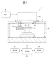
- FIG. 1 schematically shows a schematic configuration of an embodiment in which the present invention is applied to a semiconductor inspection system 1 for inspecting a semiconductor device formed on a semiconductor wafer.
- the semiconductor inspection system 1 includes a probe device 2 and a tester 3.
- the probe apparatus 2 includes a housing 2a, and a wafer mounting table 10 for mounting and holding the semiconductor wafer W by suction is disposed in the housing 2a.
- the wafer mounting table 10 includes a driving mechanism 11 and is movable in the x, y, z, and ⁇ directions.
- the wafer mounting table 10 includes a temperature control mechanism, and can cool the semiconductor wafer W sucked and held on the wafer mounting table 10 to a predetermined temperature, for example, a low temperature of about ⁇ 30 ° C.
- the casing 2a located above the wafer mounting table 10 is provided with a circular opening, and an insert ring 12 is disposed along the peripheral edge of the circular opening.
- the insert ring 12 is provided with a card clamp mechanism 13, and the probe card 20 is detachably held by the card clamp mechanism 13.
- the probe card 20 is composed of a wiring board 20a and a plurality of probes 20b electrically connected to the wiring board 20a.
- the probes 20b of the probe card 20 are arranged on the semiconductor wafer W. Are arranged corresponding to the electrodes of the semiconductor device formed in the above.
- a needle grinder 14 for polishing the tip of the probe there is a needle grinder 14 for polishing the tip of the probe, and a camera 15 that is arranged facing upward and capable of capturing an upper image. It is arranged.
- the camera 15 is composed of a CCD camera, for example, and images the probe of the probe card 20 and aligns it with the probe.
- a test head 30 connected to the tester 3 is disposed above the probe card 20. Further, an interface unit 40 is disposed between the probe card 20 and the test head 30, and the probe card 20 and the test head 30 are electrically connected via the interface unit 40. The detailed configuration of the interface unit 40 will be described later.
- the tester 3 sends an inspection signal to the semiconductor device formed on the semiconductor wafer W, and inspects the state of the semiconductor device by detecting a signal output from the semiconductor device in response to the inspection signal.
- the tester 3 and the semiconductor device formed on the semiconductor wafer W are electrically connected via the probe card 20, the interface unit 40, and the test head 30 described above.
- the semiconductor inspection system 1 includes a control unit 60 having a CPU and the like, and the operation of the semiconductor inspection system 1 is comprehensively controlled by the control unit 60.
- the control unit 60 includes an operation unit 61 and a storage unit 62.
- the operation unit 61 includes a keyboard for a command input by the process manager to manage the semiconductor inspection system 1, a display for visualizing and displaying the operating status of the semiconductor inspection system 1, and the like.
- the storage unit 62 stores a recipe that stores a control program (software), inspection condition data, and the like for realizing various operations executed by the semiconductor inspection system 1 under the control of the control unit 60. If necessary, various recipes in the semiconductor inspection system 1 are controlled under the control of the control unit 60 by calling an arbitrary recipe from the storage unit 62 according to an instruction from the operation unit 61 and causing the control unit 60 to execute the recipe. Operation is performed. Also, recipes such as control programs and processing condition data may be stored in a computer-readable computer recording medium (for example, hard disk, CD, flexible disk, semiconductor memory, etc.), or It is also possible to transmit the data from other devices as needed via a dedicated line and use it online.
- a control program software
- inspection condition data and the like for realizing various operations executed by the semiconductor inspection system 1 under the control of the control unit 60.
- various recipes in the semiconductor inspection system 1 are controlled under the control of the control unit 60 by calling an arbitrary recipe from the storage unit 62 according to an instruction from the operation unit 61 and causing the control
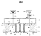
- the interface unit 40 is between the probe card (first board) 20 held by the card clamp mechanism 13 of the probe device 2 and the mother board (second board) 31 of the test head 30. It is arrange
- a frame-like base frame 41 is disposed on the interface unit 40 so as to be in contact with the mother board 31.
- a module board 32 is disposed on the mother board 31.
- a pogo block 44 having a plurality of pogo pins (spring pins) 43 as electrical connection means is disposed inside the base frame 41.
- the probe card 20 and the mother board 31 are electrically connected by these pogo pins 43.
- FIG. 2 several pogo pins 43 are schematically illustrated, but actually, for example, several thousand pogo pins 43 are disposed as a whole.
- a vacuum seal mechanism 45a made of an O-ring or the like is disposed between the mother board 31 and the base frame 41, and the space between the mother board 31 and the base frame 41 is airtightly closed.
- a vacuum seal mechanism 45b made of an O-ring or the like is disposed between the base frame 41 and the probe card 20, and the space between the base frame 41 and the probe card 20 is airtightly closed.
- the vacuum seal mechanism 45a composed of an O-ring or the like between each member arranged to be stacked in the vertical direction, that is, the mother board 31, the base frame 41, and the probe card 20, respectively. 45b, and the space 49 surrounded by the mother board 31, the base frame 41 and the probe card 20 is airtightly closed.
- a dry gas introduction path 46 is disposed in the base frame 41, and one end of a dry gas introduction pipe 46a is connected to the dry gas introduction path 46. Further, a flow rate controller 46b is inserted in the dry gas introduction pipe 46a, and the other end of the dry gas introduction pipe 46a is connected to a dry gas supply source 46c.
- a vacuum exhaust path 48 is disposed in the base frame 41, and one end of a vacuum exhaust pipe 48a is connected to the vacuum exhaust path 48.
- a vacuum exhaust mechanism 48b composed of a vacuum pump or the like is connected to the other end of the vacuum exhaust pipe 48a.
- the space 49 surrounded by the mother board 31, the base frame 41, and the probe card 20 is evacuated by the evacuation mechanism 48 b, the evacuation pipe 48 a, and the evacuation path 48.
- An atmosphere for example, a reduced pressure atmosphere having a pressure of about 10 kPa to 100 kPa (in this embodiment, about 35 kPa to 55 kPa) from atmospheric pressure is used.
- the space 49 is reduced in pressure as described above, and a predetermined amount is supplied from the dry gas supply source 46c via the flow rate controller 46b, the dry gas introduction pipe 46a, and the dry gas introduction path 46.
- a dry gas for example, dry air (dry air) is supplied into the space 49.
- the supply of the dry gas is performed with the flow rate controller 46b controlling the flow rate to a predetermined flow rate, for example, 0.1 l / min to 3 l / min, preferably 0.1 l / min to 1 l / min.
- the space 49 is maintained in a predetermined reduced-pressure atmosphere, and a dry gas having a controlled flow rate is introduced into the space 49.
- a reduced pressure atmosphere can be maintained while lowering the environmental dew point in the space 49, and condensation can be prevented.
- the environmental dew point in the space 49 can be lowered without being affected by the surrounding environmental atmosphere, and the occurrence of condensation in the space 49 is reliably prevented. be able to.
- the semiconductor inspection system 1 configured as described above is used to perform electrical inspection of the semiconductor device formed on the semiconductor wafer W
- the semiconductor wafer W is mounted on the wafer mounting table 10 of the probe apparatus 2. Place and hold by suction.
- the wafer mounting table 10 is cooled in advance to a desired inspection temperature for inspecting the semiconductor wafer W, for example, a low temperature of about ⁇ 30 ° C.
- the space 49 is evacuated to a predetermined reduced pressure atmosphere, for example, a reduced pressure atmosphere having a low pressure of about 10 kPa to 100 kPa (in this embodiment, about 35 kPa to 55 kPa) from atmospheric pressure,
- a dry gas for example, dry air (dry air) is supplied into the space 49 in a state where the flow rate is controlled to a predetermined flow rate, for example, 0.1 l / min to 3 l / min, preferably 0.1 l / min to 1 l / min. And maintain this state. This reliably prevents condensation from occurring in the interface unit 40.
- the semiconductor wafer W is moved together with the wafer mounting table 10 by the driving mechanism 11, and each electrode of the semiconductor wafer W is brought into contact with the corresponding probe 20 b of the probe card 20 to obtain electrical continuity.
- the connected tester 3 inspects the electrical characteristics of the semiconductor device.
Landscapes
- Engineering & Computer Science (AREA)
- Environmental & Geological Engineering (AREA)
- Physics & Mathematics (AREA)
- General Physics & Mathematics (AREA)
- Computer Hardware Design (AREA)
- Microelectronics & Electronic Packaging (AREA)
- General Engineering & Computer Science (AREA)
- Health & Medical Sciences (AREA)
- Toxicology (AREA)
- Testing Or Measuring Of Semiconductors Or The Like (AREA)
- Testing Of Individual Semiconductor Devices (AREA)
Abstract
Priority Applications (3)
| Application Number | Priority Date | Filing Date | Title |
|---|---|---|---|
| US14/412,650 US20150145540A1 (en) | 2012-07-02 | 2013-06-18 | Semiconductor inspection system and method for preventing condenation at interface part |
| CN201380031735.4A CN104380450A (zh) | 2012-07-02 | 2013-06-18 | 半导体检查系统及接口部的结露防止方法 |
| KR20157002657A KR20150034230A (ko) | 2012-07-02 | 2013-06-18 | 반도체 검사 시스템 및 인터페이스부의 결로 방지 방법 |
Applications Claiming Priority (2)
| Application Number | Priority Date | Filing Date | Title |
|---|---|---|---|
| JP2012-148263 | 2012-07-02 | ||
| JP2012148263A JP2014011373A (ja) | 2012-07-02 | 2012-07-02 | 半導体検査システム及びインターフェース部の結露防止方法 |
Publications (1)
| Publication Number | Publication Date |
|---|---|
| WO2014007084A1 true WO2014007084A1 (fr) | 2014-01-09 |
Family
ID=49881842
Family Applications (1)
| Application Number | Title | Priority Date | Filing Date |
|---|---|---|---|
| PCT/JP2013/067161 Ceased WO2014007084A1 (fr) | 2012-07-02 | 2013-06-18 | Système d'inspection de semi-conducteur et procédé permettant d'empêcher la condensation au niveau d'une partie d'interface |
Country Status (6)
| Country | Link |
|---|---|
| US (1) | US20150145540A1 (fr) |
| JP (1) | JP2014011373A (fr) |
| KR (1) | KR20150034230A (fr) |
| CN (1) | CN104380450A (fr) |
| TW (1) | TW201418733A (fr) |
| WO (1) | WO2014007084A1 (fr) |
Cited By (2)
| Publication number | Priority date | Publication date | Assignee | Title |
|---|---|---|---|---|
| TWI687691B (zh) * | 2018-12-17 | 2020-03-11 | 財團法人國家實驗硏究院 | 多點測試裝置 |
| CN114096933A (zh) * | 2019-07-19 | 2022-02-25 | 东京毅力科创株式会社 | 温度控制装置、温度控制方法和检查装置 |
Families Citing this family (20)
| Publication number | Priority date | Publication date | Assignee | Title |
|---|---|---|---|---|
| JP6289962B2 (ja) * | 2013-07-11 | 2018-03-07 | 東京エレクトロン株式会社 | プローブ装置 |
| EP2963430B1 (fr) * | 2014-07-03 | 2019-10-02 | Rasco GmbH | Agencement de contacteur, manipulateur de bandelette de test et agencement d'un tel manipulateur |
| JP6041175B2 (ja) * | 2015-03-30 | 2016-12-07 | 株式会社東京精密 | プローバ |
| US10732218B2 (en) * | 2015-08-26 | 2020-08-04 | Texas Instruments Incorporated | Seal monitor for probe or test chamber |
| CN108291934B (zh) * | 2015-09-29 | 2021-04-06 | 株式会社村田制作所 | 电子部件的检查装置以及检查方法 |
| KR101640434B1 (ko) * | 2015-12-21 | 2016-07-19 | (주)에스티글로벌 | 유량 측정 방식을 이용한 웨이퍼 베이킹 설비의 배기관 오염물질 제거장치 |
| JP6655516B2 (ja) * | 2016-09-23 | 2020-02-26 | 東京エレクトロン株式会社 | 基板検査装置 |
| JP6755772B2 (ja) * | 2016-10-27 | 2020-09-16 | メタウォーター株式会社 | 水処理装置 |
| TWI701436B (zh) * | 2017-11-24 | 2020-08-11 | 鴻勁精密股份有限公司 | 具防結露偵控單元之測試裝置及其應用之測試分類設備 |
| JP7058524B2 (ja) * | 2018-03-09 | 2022-04-22 | 東京エレクトロン株式会社 | 結露防止方法および処理システム |
| JP6843089B2 (ja) * | 2018-04-09 | 2021-03-17 | 東京エレクトロン株式会社 | 結露防止方法および処理装置 |
| JP7018368B2 (ja) * | 2018-07-12 | 2022-02-10 | 東京エレクトロン株式会社 | 検査装置及び検査装置の清浄化方法 |
| KR101982516B1 (ko) | 2018-08-30 | 2019-05-27 | 안병도 | 반도체 검사 장치 |
| JP7273656B2 (ja) * | 2019-08-14 | 2023-05-15 | 東京エレクトロン株式会社 | プローバおよびプローブカードのプリクール方法 |
| JP2021038999A (ja) * | 2019-09-03 | 2021-03-11 | 東京エレクトロン株式会社 | 電気的接続装置、検査装置及び接触対象体と接触子との電気的接続方法 |
| KR102844590B1 (ko) | 2020-12-07 | 2025-08-11 | 삼성전자주식회사 | 테스트 장치 및 방법 |
| KR102363332B1 (ko) * | 2021-04-02 | 2022-02-15 | 유정시스템(주) | 반도체 디바이스 패키지의 실장 테스트용 챔버 블록 및 이를 포함한 장치 |
| KR102863770B1 (ko) * | 2021-05-26 | 2025-09-23 | 세메스 주식회사 | 웨이퍼 검사 장치 및 웨이퍼 검사 방법 |
| US12092658B2 (en) * | 2021-08-18 | 2024-09-17 | Mpi Corporation | Optical detection system and alignment method for a predetermined target object |
| US20260118409A1 (en) * | 2024-10-30 | 2026-04-30 | Intest Ems, Llc | System and method for vacuum-assisted mechanical board to board latching interface system for ate test cells |
Citations (5)
| Publication number | Priority date | Publication date | Assignee | Title |
|---|---|---|---|---|
| JPH0645910Y2 (ja) * | 1987-09-30 | 1994-11-24 | 日立電子エンジニアリング株式会社 | ソケットボードの結露防止装置 |
| JPH075425Y2 (ja) * | 1987-12-09 | 1995-02-08 | 株式会社アドバンテスト | 測定部の結露防止装置 |
| JPH0758168A (ja) * | 1993-08-19 | 1995-03-03 | Tokyo Electron Ltd | プローブ装置 |
| JP2009105339A (ja) * | 2007-10-25 | 2009-05-14 | Mitsumi Electric Co Ltd | 検査装置及び検査方法 |
| JP2010101834A (ja) * | 2008-10-27 | 2010-05-06 | Yokogawa Electric Corp | 半導体試験装置 |
Family Cites Families (8)
| Publication number | Priority date | Publication date | Assignee | Title |
|---|---|---|---|---|
| US6541991B1 (en) * | 2001-05-04 | 2003-04-01 | Xilinx Inc. | Interface apparatus and method for testing different sized ball grid array integrated circuits |
| JP2006319273A (ja) * | 2005-05-16 | 2006-11-24 | Agilent Technol Inc | インターフェースアッセンブリ、及びそれを用いた乾燥ガス封入装置 |
| US8441271B2 (en) * | 2007-04-03 | 2013-05-14 | Advantest Corporation | Contactor and method of production of contactor |
| WO2009004721A1 (fr) * | 2007-07-03 | 2009-01-08 | Advantest Corporation | Sonde, carte de sondes, et procédé de fabrication de sonde |
| FR2944461B1 (fr) * | 2009-04-15 | 2011-05-20 | Air Liquide | Procede et installation de traitement de surface par jets de fluide cryogenique. |
| JP5427536B2 (ja) * | 2009-10-01 | 2014-02-26 | 東京エレクトロン株式会社 | プローブカード |
| US8975084B2 (en) * | 2010-12-16 | 2015-03-10 | Exxonmobil Research And Engineering Company | Determination of cores or building blocks and reconstruction of parent molecules in heavy petroleums and other hydrocarbon resources |
| US8959894B2 (en) * | 2011-03-24 | 2015-02-24 | GM Global Technology Operations LLC | Manganese-based oxides promoted lean NOx trap (LNT) catalyst |
-
2012
- 2012-07-02 JP JP2012148263A patent/JP2014011373A/ja active Pending
-
2013
- 2013-06-18 US US14/412,650 patent/US20150145540A1/en not_active Abandoned
- 2013-06-18 CN CN201380031735.4A patent/CN104380450A/zh active Pending
- 2013-06-18 KR KR20157002657A patent/KR20150034230A/ko not_active Withdrawn
- 2013-06-18 WO PCT/JP2013/067161 patent/WO2014007084A1/fr not_active Ceased
- 2013-07-01 TW TW102123412A patent/TW201418733A/zh unknown
Patent Citations (5)
| Publication number | Priority date | Publication date | Assignee | Title |
|---|---|---|---|---|
| JPH0645910Y2 (ja) * | 1987-09-30 | 1994-11-24 | 日立電子エンジニアリング株式会社 | ソケットボードの結露防止装置 |
| JPH075425Y2 (ja) * | 1987-12-09 | 1995-02-08 | 株式会社アドバンテスト | 測定部の結露防止装置 |
| JPH0758168A (ja) * | 1993-08-19 | 1995-03-03 | Tokyo Electron Ltd | プローブ装置 |
| JP2009105339A (ja) * | 2007-10-25 | 2009-05-14 | Mitsumi Electric Co Ltd | 検査装置及び検査方法 |
| JP2010101834A (ja) * | 2008-10-27 | 2010-05-06 | Yokogawa Electric Corp | 半導体試験装置 |
Cited By (3)
| Publication number | Priority date | Publication date | Assignee | Title |
|---|---|---|---|---|
| TWI687691B (zh) * | 2018-12-17 | 2020-03-11 | 財團法人國家實驗硏究院 | 多點測試裝置 |
| CN114096933A (zh) * | 2019-07-19 | 2022-02-25 | 东京毅力科创株式会社 | 温度控制装置、温度控制方法和检查装置 |
| CN114096933B (zh) * | 2019-07-19 | 2022-12-20 | 东京毅力科创株式会社 | 温度控制装置、温度控制方法和检查装置 |
Also Published As
| Publication number | Publication date |
|---|---|
| TW201418733A (zh) | 2014-05-16 |
| CN104380450A (zh) | 2015-02-25 |
| KR20150034230A (ko) | 2015-04-02 |
| US20150145540A1 (en) | 2015-05-28 |
| JP2014011373A (ja) | 2014-01-20 |
Similar Documents
| Publication | Publication Date | Title |
|---|---|---|
| JP2014011373A (ja) | 半導体検査システム及びインターフェース部の結露防止方法 | |
| JP7245984B2 (ja) | プローバ | |
| TWI649570B (zh) | Wafer inspection device | |
| KR102282694B1 (ko) | 검사 장치 및 콘택트 방법 | |
| JP6423660B2 (ja) | ウエハ検査装置における検査用圧力設定値決定方法 | |
| JP5789206B2 (ja) | ウエハ検査用インターフェース及びウエハ検査装置 | |
| JP6803542B2 (ja) | プローバ及びプローブ検査方法 | |
| JP5970218B2 (ja) | プローブ装置 | |
| JP6801166B2 (ja) | プローバ及びプローブ検査方法 | |
| JP2020106454A (ja) | 温度測定部材、検査装置及び温度測定方法 | |
| WO2011040134A1 (fr) | Carte sonde | |
| JP2017126729A (ja) | プローバ及びプローブコンタクト方法 | |
| JP2014029916A (ja) | プローブカードへの基板当接装置及び基板当接装置を備えた基板検査装置 | |
| JP2022173284A (ja) | プローバ及びプローブ検査方法 | |
| JP6777845B2 (ja) | プローバ及びプローブコンタクト方法 | |
| JP2023160951A (ja) | プローバ用制御装置及びプローバ用制御方法 | |
| JP2021027175A (ja) | 検査装置 | |
| WO2016159156A1 (fr) | Dispositif de sondage | |
| JP7688817B2 (ja) | プローバ及びその制御方法 | |
| JP7277845B2 (ja) | プローバ | |
| JP7369639B2 (ja) | 電子部品搬送装置の異常判断方法 | |
| JP2018041838A (ja) | プローバ | |
| JP2007292696A (ja) | 半導体装置のテスト用治具とテスト方法 | |
| JP2023083568A (ja) | プローバ及びプローブ検査方法 | |
| JP2007271313A (ja) | 基板検査装置 |
Legal Events
| Date | Code | Title | Description |
|---|---|---|---|
| 121 | Ep: the epo has been informed by wipo that ep was designated in this application |
Ref document number: 13813350 Country of ref document: EP Kind code of ref document: A1 |
|
| NENP | Non-entry into the national phase |
Ref country code: DE |
|
| WWE | Wipo information: entry into national phase |
Ref document number: 14412650 Country of ref document: US |
|
| ENP | Entry into the national phase |
Ref document number: 20157002657 Country of ref document: KR Kind code of ref document: A |
|
| 122 | Ep: pct application non-entry in european phase |
Ref document number: 13813350 Country of ref document: EP Kind code of ref document: A1 |