WO2014021030A1 - 光源ユニット - Google Patents
光源ユニット Download PDFInfo
- Publication number
- WO2014021030A1 WO2014021030A1 PCT/JP2013/067494 JP2013067494W WO2014021030A1 WO 2014021030 A1 WO2014021030 A1 WO 2014021030A1 JP 2013067494 W JP2013067494 W JP 2013067494W WO 2014021030 A1 WO2014021030 A1 WO 2014021030A1
- Authority
- WO
- WIPO (PCT)
- Prior art keywords
- strip
- wiring
- led elements
- light source
- source unit
- Prior art date
- Legal status (The legal status is an assumption and is not a legal conclusion. Google has not performed a legal analysis and makes no representation as to the accuracy of the status listed.)
- Ceased
Links
Images







Classifications
-
- F—MECHANICAL ENGINEERING; LIGHTING; HEATING; WEAPONS; BLASTING
- F21—LIGHTING
- F21V—FUNCTIONAL FEATURES OR DETAILS OF LIGHTING DEVICES OR SYSTEMS THEREOF; STRUCTURAL COMBINATIONS OF LIGHTING DEVICES WITH OTHER ARTICLES, NOT OTHERWISE PROVIDED FOR
- F21V23/00—Arrangement of electric circuit elements in or on lighting devices
- F21V23/003—Arrangement of electric circuit elements in or on lighting devices the elements being electronics drivers or controllers for operating the light source, e.g. for a LED array
- F21V23/004—Arrangement of electric circuit elements in or on lighting devices the elements being electronics drivers or controllers for operating the light source, e.g. for a LED array arranged on a substrate, e.g. a printed circuit board
- F21V23/005—Arrangement of electric circuit elements in or on lighting devices the elements being electronics drivers or controllers for operating the light source, e.g. for a LED array arranged on a substrate, e.g. a printed circuit board the substrate is supporting also the light source
-
- F—MECHANICAL ENGINEERING; LIGHTING; HEATING; WEAPONS; BLASTING
- F21—LIGHTING
- F21V—FUNCTIONAL FEATURES OR DETAILS OF LIGHTING DEVICES OR SYSTEMS THEREOF; STRUCTURAL COMBINATIONS OF LIGHTING DEVICES WITH OTHER ARTICLES, NOT OTHERWISE PROVIDED FOR
- F21V23/00—Arrangement of electric circuit elements in or on lighting devices
- F21V23/06—Arrangement of electric circuit elements in or on lighting devices the elements being coupling devices, e.g. connectors
-
- F—MECHANICAL ENGINEERING; LIGHTING; HEATING; WEAPONS; BLASTING
- F21—LIGHTING
- F21V—FUNCTIONAL FEATURES OR DETAILS OF LIGHTING DEVICES OR SYSTEMS THEREOF; STRUCTURAL COMBINATIONS OF LIGHTING DEVICES WITH OTHER ARTICLES, NOT OTHERWISE PROVIDED FOR
- F21V29/00—Protecting lighting devices from thermal damage; Cooling or heating arrangements specially adapted for lighting devices or systems
- F21V29/50—Cooling arrangements
- F21V29/70—Cooling arrangements characterised by passive heat-dissipating elements, e.g. heat-sinks
-
- H—ELECTRICITY
- H10—SEMICONDUCTOR DEVICES; ELECTRIC SOLID-STATE DEVICES NOT OTHERWISE PROVIDED FOR
- H10H—INORGANIC LIGHT-EMITTING SEMICONDUCTOR DEVICES HAVING POTENTIAL BARRIERS
- H10H20/00—Individual inorganic light-emitting semiconductor devices having potential barriers, e.g. light-emitting diodes [LED]
- H10H20/80—Constructional details
- H10H20/81—Bodies
- H10H20/813—Bodies having a plurality of light-emitting regions, e.g. multi-junction LEDs or light-emitting devices having photoluminescent regions within the bodies
-
- H—ELECTRICITY
- H10—SEMICONDUCTOR DEVICES; ELECTRIC SOLID-STATE DEVICES NOT OTHERWISE PROVIDED FOR
- H10H—INORGANIC LIGHT-EMITTING SEMICONDUCTOR DEVICES HAVING POTENTIAL BARRIERS
- H10H20/00—Individual inorganic light-emitting semiconductor devices having potential barriers, e.g. light-emitting diodes [LED]
- H10H20/80—Constructional details
- H10H20/85—Packages
- H10H20/857—Interconnections, e.g. lead-frames, bond wires or solder balls
-
- H—ELECTRICITY
- H10—SEMICONDUCTOR DEVICES; ELECTRIC SOLID-STATE DEVICES NOT OTHERWISE PROVIDED FOR
- H10W—GENERIC PACKAGES, INTERCONNECTIONS, CONNECTORS OR OTHER CONSTRUCTIONAL DETAILS OF DEVICES COVERED BY CLASS H10
- H10W72/00—Interconnections or connectors in packages
- H10W72/30—Die-attach connectors
-
- H—ELECTRICITY
- H10—SEMICONDUCTOR DEVICES; ELECTRIC SOLID-STATE DEVICES NOT OTHERWISE PROVIDED FOR
- H10W—GENERIC PACKAGES, INTERCONNECTIONS, CONNECTORS OR OTHER CONSTRUCTIONAL DETAILS OF DEVICES COVERED BY CLASS H10
- H10W90/00—Package configurations
-
- F—MECHANICAL ENGINEERING; LIGHTING; HEATING; WEAPONS; BLASTING
- F21—LIGHTING
- F21Y—INDEXING SCHEME ASSOCIATED WITH SUBCLASSES F21K, F21L, F21S and F21V, RELATING TO THE FORM OR THE KIND OF THE LIGHT SOURCES OR OF THE COLOUR OF THE LIGHT EMITTED
- F21Y2105/00—Planar light sources
- F21Y2105/10—Planar light sources comprising a two-dimensional [2D] array of point-like light-generating elements
-
- F—MECHANICAL ENGINEERING; LIGHTING; HEATING; WEAPONS; BLASTING
- F21—LIGHTING
- F21Y—INDEXING SCHEME ASSOCIATED WITH SUBCLASSES F21K, F21L, F21S and F21V, RELATING TO THE FORM OR THE KIND OF THE LIGHT SOURCES OR OF THE COLOUR OF THE LIGHT EMITTED
- F21Y2115/00—Light-generating elements of semiconductor light sources
- F21Y2115/10—Light-emitting diodes [LED]
-
- H—ELECTRICITY
- H10—SEMICONDUCTOR DEVICES; ELECTRIC SOLID-STATE DEVICES NOT OTHERWISE PROVIDED FOR
- H10W—GENERIC PACKAGES, INTERCONNECTIONS, CONNECTORS OR OTHER CONSTRUCTIONAL DETAILS OF DEVICES COVERED BY CLASS H10
- H10W72/00—Interconnections or connectors in packages
- H10W72/01—Manufacture or treatment
- H10W72/013—Manufacture or treatment of die-attach connectors
- H10W72/01308—Manufacture or treatment of die-attach connectors using permanent auxiliary members, e.g. using alignment marks
-
- H—ELECTRICITY
- H10—SEMICONDUCTOR DEVICES; ELECTRIC SOLID-STATE DEVICES NOT OTHERWISE PROVIDED FOR
- H10W—GENERIC PACKAGES, INTERCONNECTIONS, CONNECTORS OR OTHER CONSTRUCTIONAL DETAILS OF DEVICES COVERED BY CLASS H10
- H10W72/00—Interconnections or connectors in packages
- H10W72/30—Die-attach connectors
- H10W72/381—Auxiliary members
- H10W72/387—Flow barriers
-
- H—ELECTRICITY
- H10—SEMICONDUCTOR DEVICES; ELECTRIC SOLID-STATE DEVICES NOT OTHERWISE PROVIDED FOR
- H10W—GENERIC PACKAGES, INTERCONNECTIONS, CONNECTORS OR OTHER CONSTRUCTIONAL DETAILS OF DEVICES COVERED BY CLASS H10
- H10W72/00—Interconnections or connectors in packages
- H10W72/851—Dispositions of multiple connectors or interconnections
- H10W72/874—On different surfaces
- H10W72/884—Die-attach connectors and bond wires
-
- H—ELECTRICITY
- H10—SEMICONDUCTOR DEVICES; ELECTRIC SOLID-STATE DEVICES NOT OTHERWISE PROVIDED FOR
- H10W—GENERIC PACKAGES, INTERCONNECTIONS, CONNECTORS OR OTHER CONSTRUCTIONAL DETAILS OF DEVICES COVERED BY CLASS H10
- H10W90/00—Package configurations
- H10W90/701—Package configurations characterised by the relative positions of pads or connectors relative to package parts
- H10W90/731—Package configurations characterised by the relative positions of pads or connectors relative to package parts of die-attach connectors
- H10W90/734—Package configurations characterised by the relative positions of pads or connectors relative to package parts of die-attach connectors between a chip and a stacked insulating package substrate, interposer or RDL
Definitions
- the present invention relates to a light source unit, and particularly to a light source unit having a plurality of LED elements on a substrate.
- the protective film, adhesive, paint, ink, photoresist, resin, alignment film, etc. which are objects to be processed, are cured, dried, melted, or softened.
- a light source that emits ultraviolet rays is often used as a light source for performing a modification process or the like.
- LED elements that emit light in the ultraviolet region have been used, and such ultraviolet light is emitted.
- An ultraviolet light source unit using an LED element has been developed.
- a configuration in which a light source unit using the LED element is combined with an inkjet head of an inkjet printer is disclosed in Japanese Patent Application Laid-Open No. 2004-358769 (Patent Document 1).
- FIG. 15 shows the configuration.
- the ink jet printer 20 includes an ink jet head 21 that ejects ink onto a print medium M such as paper, and an ultraviolet light source unit 22 provided on one side or both sides thereof.
- the inkjet head 21 and the ultraviolet light source unit 22 are disposed above the print medium M by a predetermined distance, suspended on the guide rail 23 and scanned in the transverse direction X with respect to the print medium M.
- the UV ink droplets ejected from the inkjet head 21 and attached to the surface of the print medium M are cured by the ultraviolet rays irradiated from the light source unit 22. Thereby, the UV ink is colored on the surface of the print medium M in the scanning direction X of the inkjet head 21.
- the print medium M moves in the length direction Y by a predetermined distance, and the printing operation is repeated. Thereby, a picture or a character can be formed on the surface of the print medium.
- FIG. 17 a wiring configuration as shown in FIG. 17, a plurality of linear strip wirings 12, 12 extending in one direction are arranged in parallel on a substrate 11. A plurality of LED elements 13 and 13 are connected to the strip-shaped wiring 12 by soldering, and the LED elements 13 and 13 are arranged in a staggered pattern as the entire substrate 11.
- the wire 15 connected to the upper surface electrode 14 is electrically connected to the area
- one strip-like wiring 12 becomes a common electrode for the plurality of LED elements 13 and 13 provided thereon, and each LED element 13 and 13 on this strip-like wiring 12 is electrically connected. It will be connected in parallel.
- the LED elements 13 are joined to the band-shaped wiring 12 by soldering, and each LED element 13 is connected to the region 16 between the LED elements 13 and 13 in the adjacent band-shaped wiring 12 by the wire 15.
- the LED element 13 is soldered to the strip-shaped wiring 12
- the solder 17 and the flux contained therein are melted and flow out from the lower surface of the LED element 13. Since it is difficult to control the outflow of the solder 17, and from the viewpoint of reducing the mounting density of the LED elements 13, the adjacent LED elements 13, 13 are arranged with the smallest possible spacing. There often occurs a phenomenon in which the solder 17 that joins 13 is continuously connected to the solder that flows out from the adjacent LED element 13.
- FIG. 17 the arrangement of LED elements and strip-like wiring that can be mounted on a substrate at high density in order to realize high-density mounting of LED elements in the light source unit, as described above.
- the structure shown is examined.
- this LED element 13 has electrodes 14 and 18 on the upper surface and the lower surface, respectively.
- the electrodes 14 on the upper surface are connected by soldering or the like, and are connected between the LED elements 13 on the adjacent strip-like wiring 12 via the wires 15.
- each of the strip-like wirings 12 and 12 must be insulated in terms of an electric circuit, and of course, a predetermined insulation interval is provided therebetween.
- a heat sink HS is in contact with the lower surface of the substrate 11, and heat is dissipated from the heat sink HS by cooling air from a cooling fan, whereby the substrate 11 is cooled. With such a configuration, the heat generated from the LED element 13 is dissipated through the path of the bottom electrode 18 -the strip-like wiring 12 -the substrate 11 -the heat sink HS.
- a predetermined insulation distance is required between the strip-like wirings 12 and 12, which eventually becomes a barrier, and the LED element 13 on the strip-like wiring 12 is connected to the strip-like wiring. Accordingly, it is difficult to densely arrange them in the X direction orthogonal to 12. Therefore, the arrangement density of the LED elements 13 in the X direction is increased by arranging the plurality of LED elements 13 thereon by arranging the width of the band-like wiring 12 smaller than that of the LED elements 13. It is possible.
- a strip-like wiring 12 provided on the substrate 11 is made smaller than the width of the LED elements 13, and a plurality of LED elements 13 are arranged on each wiring 12.
- the spacing can be made smaller than the configuration of FIG.
- the LED elements 13 arranged in the X direction can be densely arranged in the X direction perpendicular to the wiring 12.
- the width L1 of the strip-like wiring 12 on the substrate 11 becomes smaller than the width of the LED element 13, as shown in FIG. Further, when the mounting density in the X direction in FIG.
- the width L1 is smaller than the width L2 of the lower surface electrode 18 of the LED element 13 (L1 ⁇ L2), and the LED element 13 reaches the heat sink HS.
- the heat radiation path becomes narrow at the strip-shaped wiring 12 portion, and the heat radiation function is hindered, and a sufficient cooling effect cannot be obtained for the LED element, resulting in a problem that the luminous efficiency of the LED element is lowered. come.
- the present invention has a plurality of strip-shaped wirings formed in parallel on a substrate, a plurality of LED elements arranged on the strip-shaped wiring, and solder on the same strip-shaped wiring.
- Each attached LED element is electrically connected to adjacent strip wiring via a wire, and the LED element is a wire extending from each LED element in a light source unit arranged in a staggered manner on the substrate as a whole.
- the present invention is intended to provide a structure capable of increasing the mounting density of the LED elements on the substrate and sufficiently cooling the LED elements to prevent a decrease in light emission efficiency.
- the light source unit of the present invention is configured such that a damming groove is formed between adjacent LED elements in the same strip-shaped wiring, and a non-outflow region in which solder does not flow out between the adjacent LED elements.
- the wire is formed and connected to the non-outflow region.
- Two damming grooves are provided between adjacent LED elements on the belt-like wiring so as to cross the belt-like wiring, and the non-outflow region is formed between the grooves. It is characterized by.
- the damming groove is formed of a dot-like recess formed continuously so as to cross the strip-shaped wiring.
- the damming groove is an annular groove formed between adjacent LED elements on the strip-like wiring, and the non-outflow region is formed in the annular groove. Further, the damming groove is an annular groove surrounding the LED element, and the non-outflow region is formed outside the annular groove. Further, the dam groove is an L-shaped groove provided at an outer position corresponding to the diagonal of the LED element, and the non-outflow region is formed outside the L-shaped groove. It is characterized by that.
- the light source unit of the present invention is characterized in that the strip-shaped wiring has a large portion and a small width portion formed in the wiring direction, and the LED element is disposed on the large portion of the strip-shaped wiring. . Further, the LED element is arranged on a large part of the strip-shaped wiring, a damming groove is formed between the LED elements, and a non-outflow region where solder does not flow out is formed on the small width part. To do. Further, the large portion of the strip electrode is formed to be significantly larger than the bottom electrode provided on the bottom surface of the LED element and in contact with the strip wiring. Further, the narrow portion of the strip electrode is formed to be narrower than the LED element.
- the LED element has a square shape, and one side of the LED element is arranged in parallel with the wiring direction of the belt-like wiring. Further, the LED elements are square-shaped, and are arranged so that diagonal lines thereof coincide with the wiring direction of the strip-shaped wiring.
- a blocking groove is formed between adjacent LED elements on the strip-shaped wiring, and a non-outflow region where solder does not flow out between the adjacent LED elements is formed. Since the wire is connected, when connecting the wire extending from the LED element on the strip wiring to the adjacent strip wiring, the solder can be directly connected to the strip wiring without interfering with it, which may cause poor connection. There is no effect. Thereby, it is not necessary to worry that the solder is continuous between the adjacent LED elements during the soldering operation of the LED elements, and the LED elements can be mounted on the belt-like wiring with high density.
- the strip-shaped wiring can be arranged closer to each other, and the LED elements on the strip-shaped wiring are arranged on the substrate. While being able to arrange
- the solder of each LED element does not continue to each other, and the configuration in which the LED elements are arranged at a higher density on the entire substrate can be adopted without any concern.
- fever from the said LED element can be thermally radiated effectively, the heat_generation
- the small width portion smaller than the LED element it is possible to realize mounting with higher density in the direction orthogonal to the wiring direction on the substrate.
- Example 1 of the light source unit of this invention The elements on larger scale (A) and sectional drawing (B) of FIG.
- FIG. FIG. 4 is a partially enlarged view (A) of FIG. 3 and a cross-sectional view (B) thereof.
- FIG. The elements on larger scale (A) and sectional drawing (B) of FIG. Partial enlarged view (A) and sectional view (B) of other embodiment 5 The top view of other Example 6.
- FIG. 1 The top view (A) and AA fragmentary sectional view (B) of other Example 10.
- FIG. The top view of other Example 11.
- FIG. The perspective view of the conventional inkjet printer.
- the light source unit The top view of the intermediate example 1 of a light source unit.
- FIG. 18 is an AA partial cross-sectional view of the intermediate example 1 shown in FIG. 17.
- FIG. FIG. 21 is a partial cross-sectional view taken along line AA in FIG. 20.
- FIG. 1 is a plan view of a light source unit of the present invention
- FIG. 2 (A) is a partially enlarged view thereof
- (B) is a sectional view thereof.
- a plurality of strip-like wirings 2 and 2 made of metal are arranged with a predetermined insulation interval on a substrate 1 made of a material having an insulating property and high thermal conductivity such as aluminum nitride.
- a material having high thermal conductivity such as copper or gold is used.
- a plurality of LED elements 3, 3 are soldered on the strip-like wiring 2, and the LED elements 3, 3 on the neighboring strip-like wirings 2, 2 are arranged so as to be shifted from each other in the wiring direction.
- the LED elements 3 and 3 are arranged in a staggered manner as a whole. And the wire 5 connected to the upper surface electrode 4 of each LED element 3 is connected to the area
- the LED element 3 has a square shape, and one side thereof is arranged in parallel with the wiring direction of the belt-like wiring 2.
- the belt-like wiring 2 is provided between the LED elements 3 on the belt-like wiring 2, in other words, between the adjacent LED elements 3 and 3.
- Two damming grooves 6 and 6 are formed so as to cross.
- the groove 6 has a triangular cross-section in the case shown in FIG. 2B, but the cross-sectional shape is not limited to this, and may be an arbitrary cross-sectional shape such as a quadrangular shape or a semicircular shape.
- the solder 7 flows out to a larger range than the LED element 3, but the solder 7 is dammed by the damming grooves 6 and 6. Stopped and no longer flows out.
- the depth, size, and number of the damming grooves 6 should be such that the solder 7 has a capacity that does not flow beyond the damming grooves 6 to the outside. Good. Thereby, a non-outflow region 8 where solder does not flow out is formed between the two damming grooves 6, 6. And the wire 5 from the LED element 3 on the adjacent strip
- the damming grooves 6 provided between the LED elements 3 and 3 on the belt-like wiring 2 are not continuous grooves as in the first embodiment of FIG. Consists of.
- three dot-like grooves 6 are provided on both sides of the LED element 3.
- FIG. 5 shows another embodiment 3 of the blocking groove 6, and the blocking groove 6 provided between the LED elements 3 and 3 on the belt-like wiring 2 is an annular groove, and is an LED element. Even if the molten solder 7 flows out from the lower part of 3, it is blocked by the annular blocking groove 6 and does not flow into the inside. Thereby, the inside of the annular dam groove 6 is formed as a non-outflow region 8. And the wire 5 from the LED element 3 on the adjacent strip
- the annular dam groove 6 may have an arbitrary planar shape such as a square shape as well as an annular shape.
- FIGS. 6 and 7 show another embodiment 4 of the dam groove 6.
- the dam groove 6 is formed in an annular shape so as to surround the LED element 3.
- the outside constitutes the non-outflow region 8.
- the shape of the tubular dam groove 6 is not limited to the illustrated rectangular shape, and may be any shape such as an annular shape.
- the LED element 3 may ride on the molten solder and rotate. According to the six shapes, the outflow direction of the solder 7 to the outside is restricted, so that the problem of rotation of the LED element 3 is also prevented.
- FIG. 8 shows another embodiment 5 of the blocking groove 6, and the blocking grooves 6 are provided in pairs at outer positions corresponding to the diagonals of the LED elements 3, and are substantially L-shaped. I am doing.
- the fifth embodiment similarly to the fourth embodiment shown in FIGS. 6 and 6, the flow of the solder 7 is restricted, and the rotation of the LED element 3 can be prevented.
- Example 9 and the following are examples in which the shape of the strip-like wiring 2 and the arrangement direction of the LED elements 3 are different.
- the belt-like wiring 2 is formed with a large portion 2a and a small width portion 2b in the wiring direction.
- the LED element 3 is arrange
- the direction of the LED element 3 and the large portion 2 a is inclined by 45 ° with respect to the wiring direction of the belt-like wiring 2.
- the strip-like wirings 2 and 2 can be arranged close to each other in a direction orthogonal to the wiring direction, so that the LED elements 3 can be arranged at high density as a whole.
- damming grooves 6 and 6 are formed between the LED elements 3 and 3 in the direction crossing the belt-like wiring 2 as in the first embodiment of FIGS. Yes.
- a non-outflow region 8 is formed on the narrow width portion 2b of the strip-shaped wiring 2, and the wires 5 from the LED elements 3 of the adjacent strip-shaped wiring 2 are connected at the small width portion 2b.
- Example 7 of FIG. 10 As in Example 3 of FIG. 5, an annular dam groove 6 is formed in the narrow portion 2 b between the LED elements 3, 3, and the inside of the annular dam 6 Is formed as a non-outflow region 8.
- Example 8 of FIG. 11 As in Example 4 of FIGS. 6 and 7, an annular dam groove 6 surrounding each LED element 3 is formed, and a small width outside the annular dam groove 6.
- a non-outflow region 8 is formed in the portion 2b.
- Example 9 of FIG. 12 as in Example 5 of FIG. 8, a pair of L-shaped damming grooves 6 are formed outward corresponding to the diagonal of the LED element 3 in the wiring direction. Also in this case, the non-outflow region 8 is formed in the small-width portion 2b outside the L-shaped dam groove 6.
- the LED element 3 and the large portion 2a of the belt-like wiring 2 are arranged at 45 ° with respect to the wiring direction. However, these are parallel to the wiring direction of the belt-like wiring 2. It may be arranged so as to be.
- FIG. 13 is a plan view
- (B) is an AA partial enlarged sectional view.
- a plurality of strip-like wirings 2 and 2 made of metal are arranged with a predetermined insulation interval on a substrate 1 made of a material having an insulating property and high thermal conductivity.
- the strip-shaped wiring 2 has a large portion 2a and a small width portion 2b repeatedly formed along the wiring direction, and the adjacent strip-shaped wirings 2 and 2 are arranged such that the large portion 2a is shifted by a predetermined interval.
- the large portion 2a and the small width portion 2b are arranged so as to face each other.
- the LED elements 3 and 3 are connected to the large portions 2a of the strip-like wirings 2 and 2 so that the LED elements 3 and 3 are arranged in a staggered pattern on the entire substrate 1.
- the LED element 3 has a square shape, and one side thereof is arranged in parallel with the wiring direction of the belt-like wiring 2.
- the LED element 3 is provided with an upper surface electrode 4 and a lower surface electrode 10 on the upper and lower surfaces thereof, and the lower surface electrode 10 is on the large portion 2 a of the strip-like wiring 2.
- the LED element 3 and the belt-like wiring 2 are electrically connected by abutting and connected by soldering or the like.
- one end of a wire 5 made of gold, for example is connected to the upper surface electrode 4, and the other end of the wire 5 is connected to the narrow portion 2 b of the adjacent strip-like wiring 2.
- each strip electrode 2 is electrically connected to the adjacent strip electrode 2 via the LED element 2 and the wire 5 provided thereon.
- a heat sink HS is in contact with the lower surface of the substrate 1, and heat from the LED element 3 is radiated from the heat sink HS through the substrate 1.
- the large portion 2a of the strip-shaped wiring 2 is as shown in FIG. 13B from the viewpoint of the connection strength with the LED element 3 and the thermal conductivity to the heat sink HS via the substrate 1.
- the width L1 is desirably at least larger than the width L2 of the lower surface electrode 5 of the LED element 3 (L1> L2). Further, if the width of the narrow portion 2b of the belt-like wiring 2 is made smaller than the width of the LED element 3, the distance between the adjacent wirings 2 and 2 can be further reduced, and the LED on the substrate 1 can be arranged.
- the mounting density of the elements 3 and 3, particularly the density in the X direction perpendicular to the wiring 2 can be increased.
- FIG. 14 shows still another embodiment.
- the direction of the LED elements 3 arranged on the strip-like wiring 2 is different from that in the embodiment of FIG.
- the LED element 3 has a square shape and is arranged so that the diagonal line thereof coincides with the wiring direction of the strip-like wiring 2.
- the large portion 2a of the belt-like wiring 2 is also inclined so that the diagonal line coincides with the wiring direction.
- the LED elements 3 can be arranged with high density in the wiring direction of the belt-like wiring 2 and with high density in both the wiring direction of the belt-like wiring 2 and the direction perpendicular thereto. Can be implemented.
- the heat sink is brought into contact with the substrate for cooling.
- the heat sink is not necessarily required.
- a damming groove is formed between adjacent LED elements soldered to the same strip-shaped wiring, and the solder flows out between the adjacent LED elements.
- the strip-shaped wiring on the substrate is formed with a large portion and a small width portion in the wiring direction, and the large portion and the small width portion are arranged to face each other between the adjacent strip-shaped wiring, and the LED element is Since it is arranged on a large part of the belt-like wiring and is arranged in a staggered manner on the entire board, in particular, the LED elements can be mounted with high density in the direction orthogonal to the wiring direction of the belt-like wiring, and Without suppressing the transmission of heat from the LED element to the substrate, the LED element can be effectively cooled to prevent a decrease in the light emission efficiency.
Landscapes
- Engineering & Computer Science (AREA)
- General Engineering & Computer Science (AREA)
- Microelectronics & Electronic Packaging (AREA)
- Led Device Packages (AREA)
Abstract
【課題】基板上の複数の帯状配線に複数のLED素子が配置されていて、同一の前記帯状配線上の各LED素子は、隣接する帯状配線にワイヤーを介して電気的に接続され、前記LED素子は、基板上で全体として千鳥状に配置されている光源ユニットにおいて、帯状配線上へのワイヤー結線に不具合が生じることがなく、LED素子を高密度に配置することができ、かつ、LED素子からの放熱を妨げることなく効果的な冷却ができる構造を提供することである。 【解決手段】同一の帯状配線において、隣接するLED素子間に堰き止め溝を形成し、該LED素子間に半田が流出しない非流出領域を形成して、該非流出領域に前記ワイヤーを結線したことを特徴とする。 また、帯状配線は、配線方向において大幅部と小幅部とが形成されていて、前記LED素子が該帯状配線の大幅部上に配置されていることを特徴とする。
Description
この発明は光源ユニットに関するものであり、特に、基板上に複数のLED素子を備えた光源ユニットに係わるものである。
従来から、印刷業界や電子工業界などにおいては、被処理対象物である保護膜、接着剤、塗料、インキ、フォトレジスト、樹脂、配向膜等に対して、硬化、乾燥、溶融、あるいは軟化、改質処理などを行う光源として紫外線を放射する光源が多用されているが、近年においては、この紫外線領域の光を発光するLED素子が利用されてきており、このような紫外線領域の光を放射するLED素子を用いた紫外線光源ユニットが開発されている。
上記LED素子を用いた光源ユニットをインクジェットプリンターのインクジェットヘッドと組み合わせた構成が、特開2004-358769号公報(特許文献1)に開示されている。
上記LED素子を用いた光源ユニットをインクジェットプリンターのインクジェットヘッドと組み合わせた構成が、特開2004-358769号公報(特許文献1)に開示されている。
図15にその構成が示されている。
インクジェットプリンター20は、紙などのプリントメディアMにインクを噴出するインクジェットヘッド21と、その片側、若しくは、両側に備えられた紫外線光源ユニット22とを有している。これらのインクジェットヘッド21および紫外線光源ユニット22は、プリントメディアMより所定間隔だけ上方に配置され、ガイドレール23に懸架されてプリントメディアMに対して横断方向Xに走査される。
前記インクジェットヘッド21から噴射されてプリントメディアMの表面に付着したUVインク滴は、光源ユニット22から照射される紫外線により硬化される。これにより、インクジェットヘッド21の走査方向Xにおいて、プリントメディアM表面にUVインクが着色される。
上記のUVインク滴の硬化後に、プリントメディアMは長さ方向Yに、決められた距離だけ移動し、上記印刷動作が繰り返される。これにより、プリントメディア表面に絵図又は文字を形成できるものである。
インクジェットプリンター20は、紙などのプリントメディアMにインクを噴出するインクジェットヘッド21と、その片側、若しくは、両側に備えられた紫外線光源ユニット22とを有している。これらのインクジェットヘッド21および紫外線光源ユニット22は、プリントメディアMより所定間隔だけ上方に配置され、ガイドレール23に懸架されてプリントメディアMに対して横断方向Xに走査される。
前記インクジェットヘッド21から噴射されてプリントメディアMの表面に付着したUVインク滴は、光源ユニット22から照射される紫外線により硬化される。これにより、インクジェットヘッド21の走査方向Xにおいて、プリントメディアM表面にUVインクが着色される。
上記のUVインク滴の硬化後に、プリントメディアMは長さ方向Yに、決められた距離だけ移動し、上記印刷動作が繰り返される。これにより、プリントメディア表面に絵図又は文字を形成できるものである。
ところで、前記特許文献1においては、インクジェットプリンターに備え付けられる紫外線光源ユニットについて、LED素子を千鳥状に配置したものが示されている。図16にその配置構造が示されていて、紫外線光源ユニット22の光照射面には、LED素子221を備えた基板222が設けられており、このLED素子221は基板222上で縦横に千鳥格子状に配置されている。このような千鳥状配置構造により、紫外線光源ユニット22を移動させた際、該紫外線光源ユニット22がたどる移動幅分の範囲に対して、隙間をあけずに万遍なく紫外線を照射することができるものとしている。
ところで、基板222上に複数のLED素子221、221を直列接続して配置すると、1つのLED素子221の配線が断線してしまった場合、直列接続された全てのLED素子221、221が断線してしまい、不点灯となってしまう。
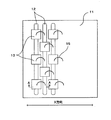
そこで本発明者らは、図17に示すような配線形態を見出した。図17において、基板11上には一方向に沿って伸びる線状の帯状配線12、12が複数並列配置されている。そして、この帯状配線12上に複数のLED素子13、13が半田付けによって接続されていて、基板11全体としてLED素子13、13が千鳥状になるよう配置されている。そして、帯状配線12上の各LED素子13では、その上面電極14に接続されたワイヤー15が、隣接する帯状配線12における各LED素子13、13の間の領域16に、所謂ワイヤーボンディングにより、電気的に接続されている。
そこで本発明者らは、図17に示すような配線形態を見出した。図17において、基板11上には一方向に沿って伸びる線状の帯状配線12、12が複数並列配置されている。そして、この帯状配線12上に複数のLED素子13、13が半田付けによって接続されていて、基板11全体としてLED素子13、13が千鳥状になるよう配置されている。そして、帯状配線12上の各LED素子13では、その上面電極14に接続されたワイヤー15が、隣接する帯状配線12における各LED素子13、13の間の領域16に、所謂ワイヤーボンディングにより、電気的に接続されている。
このような構成とすることで、1つの帯状配線12は、その上に設けられた複数のLED素子13、13の共通電極となり、この帯状配線12上の各LED素子13、13は電気的に並列接続されることになる。
このような配線構造とすることによって、LED素子13のワイヤー15が1本断線したとしても、それに付随して他の複数のLED素子13、13が点灯不能になることがないという利点がある。
このような配線構造とすることによって、LED素子13のワイヤー15が1本断線したとしても、それに付随して他の複数のLED素子13、13が点灯不能になることがないという利点がある。
しかしながら、上記構成の具体化を試みた際に、LED素子と帯状配線とをつなぐワイヤーの結線に接続不良の問題が発生することが判明した。
図18に基づいてこの不具合について説明する。
前述したように、LED素子13は帯状配線12上に半田付けによって接合され、各LED素子13は、隣接する帯状配線12におけるLED素子13、13の間の領域16にワイヤー15により結線されるが、LED素子13を帯状配線12に半田付けする際に、半田17やこれに含まれるフラックスが溶融してLED素子13の下面から流れ出す。この半田17の流出をコントロールすることは難しく、かつ、LED素子13の実装密度を小さくする観点から、隣接するLED素子13、13はできるだけ間隔を小さくして配置されるために、ひとつのLED素子13を接合する半田17が、隣接するLED素子13から流出した半田と連続的に繋がってしまうという現象がしばしば発生する。
図18に基づいてこの不具合について説明する。
前述したように、LED素子13は帯状配線12上に半田付けによって接合され、各LED素子13は、隣接する帯状配線12におけるLED素子13、13の間の領域16にワイヤー15により結線されるが、LED素子13を帯状配線12に半田付けする際に、半田17やこれに含まれるフラックスが溶融してLED素子13の下面から流れ出す。この半田17の流出をコントロールすることは難しく、かつ、LED素子13の実装密度を小さくする観点から、隣接するLED素子13、13はできるだけ間隔を小さくして配置されるために、ひとつのLED素子13を接合する半田17が、隣接するLED素子13から流出した半田と連続的に繋がってしまうという現象がしばしば発生する。
図18(A)(B)に示すように、隣接するLED素子13、13間で半田17が連続的に接合してしまうと、その間の領域16上には半田17が存在するということになる。隣接する帯状配線12のLED素子13の上面電極14から延びるワイヤー15はこの領域16にワイヤーディングされることになるが、その上面に半田17が介在するためにうまく接続することができず、結線不良を引き起こすことになる。
また、このようなインクジェットプリンターにおいて、印刷の速度を増して処理スピードをアップしようとする場合、インクジェットおよび光源ユニットを横断方向Xに素早く動かすことが必要となる。しかしながら、光源ユニットをX方向に素早く動かすと、インクジェットヘッドから噴射されたUVインク滴に照射される単位時間当たりの紫外線照射量が少なくなり、インクを十分に硬化させることができなくなる。処理のスピードアップを図ったうえで、インクの硬化を完全にするには、紫外線照射量を増大させることが必要であり、そのためには、基板上の同一面積内に、LED素子を高密度に実装することが必要となってくる。
そこで、本発明者は、光源ユニットにおけるLED素子の高密度な実装を実現すべく、基板上で高密度に実装可能なLED素子の配置及び帯状配線について、先に述べたように、図17に示すような構造を検討した。
ところで、図17のA-A断面図である図19に示すように、このLED素子13は上面と下面にそれぞれ電極14、18を有しており、この下面の電極18が帯状配線12上に半田付け等により接続されていて、上面の電極14がワイヤー15を介して隣り合う帯状配線12上のLED素子13間に結線される。
また、各々の帯状配線12、12は電気回路的に絶縁されていなければならず、当然その間には所定の絶縁間隔が設けられている。
そして、前記基板11の下面にはヒートシンクHSが当接されていて、冷却ファンからの冷却風によってヒートシンクHSから放熱し、これにより基板11が冷却されている。このような構成により、LED素子13から発生する熱は、下面電極18-帯状配線12-基板11-ヒートシンクHSの経路を経て放熱されている。
また、各々の帯状配線12、12は電気回路的に絶縁されていなければならず、当然その間には所定の絶縁間隔が設けられている。
そして、前記基板11の下面にはヒートシンクHSが当接されていて、冷却ファンからの冷却風によってヒートシンクHSから放熱し、これにより基板11が冷却されている。このような構成により、LED素子13から発生する熱は、下面電極18-帯状配線12-基板11-ヒートシンクHSの経路を経て放熱されている。
ところで、上記図17の構成によれば、帯状配線12、12間に所定の絶縁距離が必要であり、結局このことが障壁となって、この帯状配線12上のLED素子13を、該帯状配線12と直交するX方向において密に配設することが困難となっている。
そこで、上記帯状配線12の幅をLED素子13よりも小さくして配列し、その上に複数個のLED素子13を設ける構成とすることによって、X方向でのLED素子13の配設密度を高めることが考えられる。
そこで、上記帯状配線12の幅をLED素子13よりも小さくして配列し、その上に複数個のLED素子13を設ける構成とすることによって、X方向でのLED素子13の配設密度を高めることが考えられる。
図20にその態様が示されている。同図において、基板11上に設けられる帯状配線12は、LED素子13の幅よりも小幅にされていて、各配線12上に複数のLED素子13が配列されている。
帯状配線12の幅を小さくしたことによって、隣接する各配線12の間に所定の絶縁距離をとったとしても、その間隔を前記図17の構成よりも小さくして配列できて、この配線12上に配置されるLED素子13を、前記配線12と直交するX方向において密に配置できるものである。
しかしながら、このような構成を採用すると、図20のA-A断面図である図21に示されるように、基板11上の帯状配線12の幅L1が、LED素子13の幅よりも小さくなり、更に図20におけるX方向の実装密度をより小さなものとする場合、その幅L1は、LED素子13の下面電極18の幅L2よりも小さくなり(L1<L2)、LED素子13からヒートシンクHSに至る熱の放熱経路が前記帯状配線12部分で狭くなって放熱機能が妨げられてしまい、LED素子に対して十分な冷却効果が得られず、該LED素子の発光効率が低下するという問題が生じてくる。
帯状配線12の幅を小さくしたことによって、隣接する各配線12の間に所定の絶縁距離をとったとしても、その間隔を前記図17の構成よりも小さくして配列できて、この配線12上に配置されるLED素子13を、前記配線12と直交するX方向において密に配置できるものである。
しかしながら、このような構成を採用すると、図20のA-A断面図である図21に示されるように、基板11上の帯状配線12の幅L1が、LED素子13の幅よりも小さくなり、更に図20におけるX方向の実装密度をより小さなものとする場合、その幅L1は、LED素子13の下面電極18の幅L2よりも小さくなり(L1<L2)、LED素子13からヒートシンクHSに至る熱の放熱経路が前記帯状配線12部分で狭くなって放熱機能が妨げられてしまい、LED素子に対して十分な冷却効果が得られず、該LED素子の発光効率が低下するという問題が生じてくる。
この発明は、上記技術の問題点に鑑みて、基板上に複数の帯状配線が並列して形成され、該帯状配線上に複数のLED素子が配置されていて、同一の前記帯状配線上に半田付けされた各LED素子は、隣接する帯状配線にワイヤーを介して電気的に接続され、前記LED素子は、基板上で全体として千鳥状に配置されている光源ユニットにおいて、各LED素子から延びるワイヤーが隣接する帯状配線上に確実に接続されて結線不良を起こすことがない構造を提供するものである。
また、前記基板上での前記LED素子の実装密度を高めるとともに、該LED素子の冷却を十分に行えて発光効率の低下を防止することができる構造を提供せんとするものである。
また、前記基板上での前記LED素子の実装密度を高めるとともに、該LED素子の冷却を十分に行えて発光効率の低下を防止することができる構造を提供せんとするものである。
上記課題を解決するために、この発明の光源ユニットは、前記同一の帯状配線において、隣接するLED素子間に堰き止め溝を形成し、該隣接するLED素子間に半田が流出しない非流出領域を形成して、該非流出領域に前記ワイヤーを結線したことを特徴とする。
また、前記堰き止め溝が、前記帯状配線上の隣接するLED素子間で、該帯状配線を横断するように2本ずつ設けられており、該溝間に前記非流出領域を形成していることを特徴とする。
また、前記堰き止め溝が、前記帯状配線を横断するように連続して形成されたドット状の凹部からなることを特徴とする。
また、前記堰き止め溝が、前記帯状配線上の隣接するLED素子間に形成された環状溝であり、該環状溝内に前記非流出領域を形成していることを特徴とする。
また、前記堰き止め溝が、前記LED素子を取り囲む環状溝であり、該環状溝の外方に前記非流出領域を形成していることを特徴とする。
また、前記堰き止め溝が、前記LED素子の対角に対応した外方位置に設けられたL字状の溝であり、該L字状溝の外方に前記非流出領域を形成していることを特徴とする。
また、前記堰き止め溝が、前記帯状配線上の隣接するLED素子間で、該帯状配線を横断するように2本ずつ設けられており、該溝間に前記非流出領域を形成していることを特徴とする。
また、前記堰き止め溝が、前記帯状配線を横断するように連続して形成されたドット状の凹部からなることを特徴とする。
また、前記堰き止め溝が、前記帯状配線上の隣接するLED素子間に形成された環状溝であり、該環状溝内に前記非流出領域を形成していることを特徴とする。
また、前記堰き止め溝が、前記LED素子を取り囲む環状溝であり、該環状溝の外方に前記非流出領域を形成していることを特徴とする。
また、前記堰き止め溝が、前記LED素子の対角に対応した外方位置に設けられたL字状の溝であり、該L字状溝の外方に前記非流出領域を形成していることを特徴とする。
更に、この発明の光源ユニットは、前記帯状配線は、配線方向において大幅部と小幅部とが形成されていて、前記LED素子が該帯状配線の大幅部上に配置されていることを特徴とする。
また、前記LED素子が前記帯状配線の大幅部上に配置されており、前記LED素子間に堰き止め溝を形成し、前記小幅部上に半田が流出しない非流出領域を形成したことを特徴とする。
また、前記帯状電極の大幅部は、前記LED素子の下面に設けられて前記帯状配線に当接する下面電極よりも大幅に形成されていることを特徴とする。
また、前記帯状電極の小幅部は、前記LED素子よりも小幅に形成されていることを特徴とする。
また、前記LED素子は正方形状であり、その一辺が、前記帯状配線の配線方向と平行に配置されていることを特徴とする。
また、前記LED素子は正方形状であり、その対角線が前記帯状配線の配線方向に一致するように配置されていることを特徴とする。
また、前記LED素子が前記帯状配線の大幅部上に配置されており、前記LED素子間に堰き止め溝を形成し、前記小幅部上に半田が流出しない非流出領域を形成したことを特徴とする。
また、前記帯状電極の大幅部は、前記LED素子の下面に設けられて前記帯状配線に当接する下面電極よりも大幅に形成されていることを特徴とする。
また、前記帯状電極の小幅部は、前記LED素子よりも小幅に形成されていることを特徴とする。
また、前記LED素子は正方形状であり、その一辺が、前記帯状配線の配線方向と平行に配置されていることを特徴とする。
また、前記LED素子は正方形状であり、その対角線が前記帯状配線の配線方向に一致するように配置されていることを特徴とする。
この発明の光源ユニットによれば、帯状配線上の隣接するLED素子間に堰き止め溝を形成し、該隣接するLED素子間に半田が流出しない非流出領域を形成して、該非流出領域に前記ワイヤーを結線したので、帯状配線上のLED素子から延びるワイヤーを隣接する帯状配線上に接続するときに、半田が邪魔をすることがなく帯状配線上に直接結線できるので、結線不良を引き起こすことがないという効果を奏するものである。
これにより、LED素子の半田付け作業時に、隣接するLED素子間で半田が連続してしまうことを心配する必要がなくなり、LED素子を帯状配線上に高密度で実装することができる。
これにより、LED素子の半田付け作業時に、隣接するLED素子間で半田が連続してしまうことを心配する必要がなくなり、LED素子を帯状配線上に高密度で実装することができる。
更に、この発明の光源ユニットによれば、帯状配線に大幅部と小幅部を形成したので、帯状配線相互をより近接させて配置することができて、該帯状配線上のLED素子を基板上でより高密度に配置することができるとともに、前記大幅部上にLED素子を配置したので、その冷却効果を損なうことなく、発光効率の低下を防止できるという効果を奏するものである。
また、前記LED素子が前記帯状配線の大幅部上に半田付けされて配置されており、前記LED素子間に堰き止め溝を形成し、前記小幅部上に半田が流出しない非流出領域を形成したので、各LED素子の半田が互いに連続してしまうことがなく、基板全体でLED素子をより一層高密度に配置する構成を危惧なく採用することができる。
また、前記大幅部をLED素子よりも大幅にすることで、前記LED素子からの熱を効果的に放熱できて、前記LED素子の発熱を抑制し、その発光効率の低下を防止できる。
また、前記小幅部をLED素子よりも小幅とすることで、基板上の配線方向と直交する方向で、より一層高密度な実装が実現できる。
また、前記LED素子が前記帯状配線の大幅部上に半田付けされて配置されており、前記LED素子間に堰き止め溝を形成し、前記小幅部上に半田が流出しない非流出領域を形成したので、各LED素子の半田が互いに連続してしまうことがなく、基板全体でLED素子をより一層高密度に配置する構成を危惧なく採用することができる。
また、前記大幅部をLED素子よりも大幅にすることで、前記LED素子からの熱を効果的に放熱できて、前記LED素子の発熱を抑制し、その発光効率の低下を防止できる。
また、前記小幅部をLED素子よりも小幅とすることで、基板上の配線方向と直交する方向で、より一層高密度な実装が実現できる。
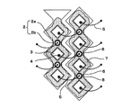
図1は、本発明の光源ユニットの平面図で、図2(A)はその部分拡大図、(B)はその断面図である。
図1に示されるように、例えば窒化アルミニウム等の絶縁性かつ熱伝導率の高い物質からなる基板1上には、金属からなる複数の帯状配線2、2が所定の絶縁間隔をもって配置されている。該帯状配線2を構成する金属は、例えば銅や金などの熱伝導率の高い材料が用いられる。
前記帯状配線2上に複数のLED素子3、3が半田付けされていて、隣接する帯状配線2、2上のLED素子3、3が配線方向において互いにずれるように配置されることにより、基板1全体でLED素子3、3は千鳥状に配置される。
そして、各LED素子3の上面電極4に接続されたワイヤー5が、隣接する帯状配線2のLED素子3、3の間の領域に結線されている。
なお、この例では、前記LED素子3は正方形状であって、その一辺が前記帯状配線2の配線方向と平行に配置されている。
図1に示されるように、例えば窒化アルミニウム等の絶縁性かつ熱伝導率の高い物質からなる基板1上には、金属からなる複数の帯状配線2、2が所定の絶縁間隔をもって配置されている。該帯状配線2を構成する金属は、例えば銅や金などの熱伝導率の高い材料が用いられる。
前記帯状配線2上に複数のLED素子3、3が半田付けされていて、隣接する帯状配線2、2上のLED素子3、3が配線方向において互いにずれるように配置されることにより、基板1全体でLED素子3、3は千鳥状に配置される。
そして、各LED素子3の上面電極4に接続されたワイヤー5が、隣接する帯状配線2のLED素子3、3の間の領域に結線されている。
なお、この例では、前記LED素子3は正方形状であって、その一辺が前記帯状配線2の配線方向と平行に配置されている。
そして、特に図2(A)(B)で明示されるように、帯状配線2上の各LED素子3の両側、換言すれば、隣接するLED素子3、3の間には、帯状配線2を横断するように2本の堰き止め溝6、6が形成されている。この溝6は、図2(B)に示されたものでは断面三角形状であるが、その断面形状はこれに限られず、四角形状、半円形状など任意の断面形状であってよい。
同図に示されるように、帯状配線2へのLED素子3の半田付け時には、半田7がLED素子3よりも大きな範囲に流れ出るが、該半田7は、前記堰き止め溝6、6によって、堰き止められて、それ以上外方には流出しない。
換言すると、前記堰き止め溝6の深さ、大きさ、更には本数は、この半田7が堰き止め溝6を越えてそれ以上外方に流出しないような容量を持たせるだけのものとすればよい。
これにより、前記2本の堰き止め溝6、6間には半田が流出しない非流出領域8が形成される。
そして、隣接する帯状配線2上のLED素子3からのワイヤー5は、この非流出領域8において帯状配線2に結線される。
同図に示されるように、帯状配線2へのLED素子3の半田付け時には、半田7がLED素子3よりも大きな範囲に流れ出るが、該半田7は、前記堰き止め溝6、6によって、堰き止められて、それ以上外方には流出しない。
換言すると、前記堰き止め溝6の深さ、大きさ、更には本数は、この半田7が堰き止め溝6を越えてそれ以上外方に流出しないような容量を持たせるだけのものとすればよい。
これにより、前記2本の堰き止め溝6、6間には半田が流出しない非流出領域8が形成される。
そして、隣接する帯状配線2上のLED素子3からのワイヤー5は、この非流出領域8において帯状配線2に結線される。
図3、4には堰き止め溝6の形状の他の実施例2が示されている。図に示すように、帯状配線2上のLED素子3、3の間に設けられる堰き止め溝6が、図1の実施例1のように連続溝ではなく、連続するドット状の凹部9、9からなる。この例では、LED素子3の両側にドット状溝6が3本ずつ設けられている。
図5には堰き止め溝6の他の実施例3が示されていて、帯状配線2上のLED素子3、3の間に設けられる堰き止め溝6は、環状の溝であって、LED素子3の下部から溶融半田7が流出しても、前記環状堰き止め溝6によって堰き止められてその内部には流入しない。これにより、該環状堰き止め溝6の内部が非流出領域8として形成される。そして、隣接する帯状配線2上のLED素子3からのワイヤー5はこの非流出領域8において帯状配線2に結線される。
なお、該環状堰き止め溝6は円環状のみならず、四角形状など任意の平面形状であってよい。
なお、該環状堰き止め溝6は円環状のみならず、四角形状など任意の平面形状であってよい。
図6、7には堰き止め溝6の他の実施例4が示されていて、この堰き止め溝6は、LED素子3を取り囲むように環状に形成されていて、該環状堰き止め溝6の外方が非流出領域8を構成する。図7(A)(B)に示すように、LED素子3の半田付け時に、その下方から溶融流出する半田7は、この管状堰き止め溝6によって堰き止められて、それ以上外方に流出することがなく、この環状堰き止め溝6の外方が非流出領域8を形成する。
なお、この場合も、管状堰き止め溝6の形状は、図示された四角形状に限られず、円環状など任意の形状であってよい。
また、半田7が何も規制を受けずに自由な方向に流出すると、LED素子3がこの溶融半田に乗って回転してしまうという惧れがあるが、この実施例4のような堰き止め溝6形状によれば、半田7の外方への流出方向が規制されるので、LED素子3の回転という不具合も防止される。
なお、この場合も、管状堰き止め溝6の形状は、図示された四角形状に限られず、円環状など任意の形状であってよい。
また、半田7が何も規制を受けずに自由な方向に流出すると、LED素子3がこの溶融半田に乗って回転してしまうという惧れがあるが、この実施例4のような堰き止め溝6形状によれば、半田7の外方への流出方向が規制されるので、LED素子3の回転という不具合も防止される。
図8には堰き止め溝6の他の実施例5が示されていて、この堰き止め溝6は、LED素子3の対角に対応した外方位置に一対設けられていて、略L字状をなしている。
この実施例5においても、前記図6、6の実施例4と同様に、半田7の流れに規制が働き、LED素子3の回転が防止できる。
この実施例5においても、前記図6、6の実施例4と同様に、半田7の流れに規制が働き、LED素子3の回転が防止できる。
図9以下は、帯状配線2の形状と、LED素子3の配置向きが異なる実施例である。
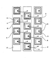
図9に示す実施例6おいて、帯状配線2にはその配線方向に大幅部2aと小幅部2bとが形成されている。そして、前記大幅部2a上にLED素子3が配置されている。このとき、LED素子3および大幅部2aの向きが帯状配線2の配線方向に対して45°だけ傾いている。このような配置構造とすることにより、帯状配線2、2を配線方向と直交する方向に近接させて蜜に配置できるので、全体としてLED素子3の高密度な配置が可能となる。
そして、この場合も、LED素子3、3の間には、前記図1、2の実施例1と同様に、帯状配線2を横断する方向に2本の堰き止め溝6、6が形成されている。
この堰き止め溝6、6により、帯状配線2の小幅部2b上に非流出領域8が形成され、隣接する帯状配線2のLED素子3からのワイヤー5は、該小幅部2bにおいて結線される。
図9に示す実施例6おいて、帯状配線2にはその配線方向に大幅部2aと小幅部2bとが形成されている。そして、前記大幅部2a上にLED素子3が配置されている。このとき、LED素子3および大幅部2aの向きが帯状配線2の配線方向に対して45°だけ傾いている。このような配置構造とすることにより、帯状配線2、2を配線方向と直交する方向に近接させて蜜に配置できるので、全体としてLED素子3の高密度な配置が可能となる。
そして、この場合も、LED素子3、3の間には、前記図1、2の実施例1と同様に、帯状配線2を横断する方向に2本の堰き止め溝6、6が形成されている。
この堰き止め溝6、6により、帯状配線2の小幅部2b上に非流出領域8が形成され、隣接する帯状配線2のLED素子3からのワイヤー5は、該小幅部2bにおいて結線される。
以下、図10の実施例7では、前記図5の実施例3と同様に、LED素子3、3間の小幅部2bに環状堰き止め溝6が形成されていて、該環状せき止め溝6の内部が非流出領域8として形成されている。
図11の実施例8では、前記図6、7の実施例4と同様に、各LED素子3を取り囲む環状堰き止め溝6が形成されていて、該環状堰き止め溝6の外方にある小幅部2bに非流出領域8が形成されている。
図12の実施例9では、前記図8の実施例5と同様に、LED素子3の配線方向の対角に対応した外方に一対のL字状堰き止め溝6が形成されている。この場合も、L字状堰き止め溝6の外方にある小幅部2bにおいて非流出領域8が形成されている。
図11の実施例8では、前記図6、7の実施例4と同様に、各LED素子3を取り囲む環状堰き止め溝6が形成されていて、該環状堰き止め溝6の外方にある小幅部2bに非流出領域8が形成されている。
図12の実施例9では、前記図8の実施例5と同様に、LED素子3の配線方向の対角に対応した外方に一対のL字状堰き止め溝6が形成されている。この場合も、L字状堰き止め溝6の外方にある小幅部2bにおいて非流出領域8が形成されている。
なお、図9以下の実施例においては、LED素子3および帯状配線2の大幅部2aが配線方向に対して45°傾いた配置構造を示したが、これらが帯状配線2の配線方向と平行になるように配置されたものであってもよい。
また、帯状配線と、LED素子の下面電極の構造を示す他の実施例について図13以下の図面に基づいて説明する。
図13において、(A)は平面図であり、(B)はA-A部分拡大断面図である。
図13(A)に示されるように、絶縁性かつ熱伝導率の高い物質からなる基板1上には、金属からなる複数の帯状配線2、2が所定の絶縁間隔をもって配置されている。
この帯状配線2は、その配線方向に沿って、大幅部2aと小幅部2bとが繰り返し形成されており、隣接する帯状配線2、2ではその大幅部2aが一定間隔だけずれるように配置されていて、隣接する帯状配線2、2間では互いに大幅部2aと小幅部2bとが対向するように配置されている。
そして、これら帯状配線2、2の大幅部2a上にLED素子3、3が接続されることにより、基板1全体でLED素子3、3は千鳥状に配置される。
なお、この例では、前記LED素子3は正方形状であって、その一辺が前記帯状配線2の配線方向と平行に配置されている。
図13において、(A)は平面図であり、(B)はA-A部分拡大断面図である。
図13(A)に示されるように、絶縁性かつ熱伝導率の高い物質からなる基板1上には、金属からなる複数の帯状配線2、2が所定の絶縁間隔をもって配置されている。
この帯状配線2は、その配線方向に沿って、大幅部2aと小幅部2bとが繰り返し形成されており、隣接する帯状配線2、2ではその大幅部2aが一定間隔だけずれるように配置されていて、隣接する帯状配線2、2間では互いに大幅部2aと小幅部2bとが対向するように配置されている。
そして、これら帯状配線2、2の大幅部2a上にLED素子3、3が接続されることにより、基板1全体でLED素子3、3は千鳥状に配置される。
なお、この例では、前記LED素子3は正方形状であって、その一辺が前記帯状配線2の配線方向と平行に配置されている。
図13(B)に示されるように、前記LED素子3には、その上下面に上面電極4と下面電極10が設けられていて、前記下面電極10が前記帯状配線2の大幅部2a上に当接されてハンダ付け等により接続され、前記LED素子3と帯状配線2が電気的に接続されている。
そして、上面電極4には、例えば金からなるワイヤー5の一端が結線され、該ワイヤー5の他端は隣設する帯状配線2の小幅部2bに結線されている。
これにより、各帯状電極2は、その上に設けられたLED素子2およびワイヤー5を介して、隣接する帯状電極2と電気的に接続されている。
そして、基板1の下面にはヒートシンクHSが当接されており、LED素子3からの熱は基板1を介して該ヒートシンクHSから放熱される。
そして、上面電極4には、例えば金からなるワイヤー5の一端が結線され、該ワイヤー5の他端は隣設する帯状配線2の小幅部2bに結線されている。
これにより、各帯状電極2は、その上に設けられたLED素子2およびワイヤー5を介して、隣接する帯状電極2と電気的に接続されている。
そして、基板1の下面にはヒートシンクHSが当接されており、LED素子3からの熱は基板1を介して該ヒートシンクHSから放熱される。
前記構成において、前記帯状配線2の大幅部2aは、LED素子3との接続強度、および基板1を介したヒートシンクHSへの熱伝導性の観点から、図13(B)に示されるように、その幅L1が、少なくとも、LED素子3の下面電極5の幅L2よりも大きい(L1>L2)ことが望ましい。
また、帯状配線2の小幅部2bの幅は、LED素子3の幅よりも小さくすれば、隣接する配線2、2の間隔をより一層小さくして配置することができ、基板1上でのLED素子3、3の実装密度、特に、配線2と直行するX方向での密度を高めることができる。
また、帯状配線2の小幅部2bの幅は、LED素子3の幅よりも小さくすれば、隣接する配線2、2の間隔をより一層小さくして配置することができ、基板1上でのLED素子3、3の実装密度、特に、配線2と直行するX方向での密度を高めることができる。
図14に、更に他の実施例が示されている。この実施例では、図13の実施例と比較して、帯状配線2上に配置されるLED素子3の向きが異なっている。LED素子3は正方形状であり、その対角線が帯状配線2の配線方向と一致するように配置されている。この場合、帯状配線2の大幅部2aもその対角線が配線方向に一致するように傾けられている。
上記構成により、図13の実施例との比較において、LED素子3は、帯状配線2の配線方向でも高密度に配置でき、帯状配線2の配線方向およびこれと直行する方向の両方向で高密度に実装することができる。
上記構成により、図13の実施例との比較において、LED素子3は、帯状配線2の配線方向でも高密度に配置でき、帯状配線2の配線方向およびこれと直行する方向の両方向で高密度に実装することができる。
なお、上記実施例においては、基板にヒートシンクを当接させて冷却するものとしたが、基板に冷却風を当てるのみでLED素子の冷却が図られる場合には、必ずしもヒートシンクを必要とはしない。
以上説明したように、本発明のLED素子を用いた光源ユニットでは、同一の帯状配線に半田付けされた隣接するLED素子間に堰き止め溝を形成し、該隣接するLED素子間に半田が流出しない非流出領域を形成することにより、隣接する帯状配線上のLED素子から延びるワイヤーを前記非流出領域に結線することができ、半田が介在することによる結線不良という不具合を起こすことがない。
また、前記基板上の帯状配線に、配線方向において大幅部と小幅部とが形成され、隣接する帯状配線間で前記大幅部と小幅部がそれぞれ対向するように配置されていて、LED素子が該帯状配線の大幅部上に配置されて、基板上の全体で千鳥状に配置されているので、特に、LED素子を帯状配線の配線方向と直交する方向で高密度に実装することができ、また、LED素子からの熱を基板に伝達することを抑制せずに、該LED素子の冷却を効果的に行えてその発光効率の低下を防止できるものである。
1 基板
2 帯状配線
2a 大幅部
2b 小幅部
3 LED素子
4 上面電極
5 ワイヤー
6 堰き止め溝
7 半田
8 非流出領域
9 ドット状凹部
10 下面電極
HS ヒートシンク
2 帯状配線
2a 大幅部
2b 小幅部
3 LED素子
4 上面電極
5 ワイヤー
6 堰き止め溝
7 半田
8 非流出領域
9 ドット状凹部
10 下面電極
HS ヒートシンク
Claims (12)
- 基板上に複数の帯状配線が並列して形成され、
該帯状配線上に複数のLED素子が配置されていて、同一の前記帯状配線上に半田付けされた各LED素子は、隣接する帯状配線にワイヤーを介して電気的に接続され、
前記LED素子は、基板上で全体として千鳥状に配置され、
ている光源ユニットにおいて、
前記同一の帯状配線において、隣接するLED素子間に堰き止め溝を形成し、該隣接するLED素子間に半田が流出しない非流出領域を形成して、該非流出領域に前記ワイヤーを結線したことを特徴とする光源ユニット。 - 前記堰き止め溝が、前記帯状配線上の隣接するLED素子間で、該帯状配線を横断するように2本ずつ設けられており、該溝間に前記非流出領域を形成していることを特徴とする請求項1に記載の光源ユニット。
- 前記堰き止め溝が、前記帯状配線を横断するように連続して形成されたドット状の凹部からなることを特徴とする請求項2に記載の光源ユニット。
- 前記堰き止め溝が、前記帯状配線上の隣接するLED素子間に形成された環状溝であり、該環状溝内に前記非流出領域を形成していることを特徴とする請求項1に記載の光源ユニット。
- 前記堰き止め溝が、前記LED素子を取り囲む環状溝であり、該環状溝の外方に前記非流出領域を形成していることを特徴とする請求項1に記載の光源ユニット。
- 前記堰き止め溝が、前記LED素子の対角に対応した外方位置に設けられたL字状の溝であり、該L字状溝の外方に前記非流出領域を形成していることを特徴とする請求項1に記載の光源ユニット。
- 基板上に複数の帯状配線が並列して形成され、
該帯状配線上に複数のLED素子が配置されていて、同一の前記帯状配線上のLED素子は、隣接する帯状配線にワイヤーを介して電気的に接続され、
前記LED素子は、基板上で全体として千鳥状に配置され、
ている光源ユニットにおいて、
前記帯状配線は、配線方向において大幅部と小幅部とが形成されていて、前記LED素子が該帯状配線の大幅部上に配置されていることを特徴とする光源ユニット。 - 前記LED素子は前記帯状配線上に半田付けされ、
前記帯状配線において、隣接するLED素子間に堰き止め溝を形成し、前記小幅部上に半田が流出しない非流出領域を形成していることを特徴とする請求項7に記載の光源ユニット。 - 前記帯状電極の大幅部は、前記LED素子の下面に設けられて前記帯状配線に当接する下面電極よりも大幅に形成されていることを特徴とする請求項7に記載の光源ユニット。
- 前記帯状電極の小幅部は、前記LED素子よりも小幅に形成されていることを特徴とする請求項7に記載の光源ユニット。
- 前記LED素子は正方形状であり、その一辺が、前記帯状配線の配線方向と平行に配置されていることを特徴とする請求項7に記載の光源ユニット。
- 前記LED素子は正方形状であり、その対角線が前記帯状配線の配線方向に一致するように配置されていることを特徴とする請求項7に記載の光源ユニット。
Priority Applications (3)
| Application Number | Priority Date | Filing Date | Title |
|---|---|---|---|
| CN201380035070.4A CN104412400B (zh) | 2012-07-30 | 2013-06-26 | 光源单元 |
| EP13826194.6A EP2882002B1 (en) | 2012-07-30 | 2013-06-26 | Light source unit |
| US14/417,620 US9755126B2 (en) | 2012-07-30 | 2013-06-26 | Light source unit |
Applications Claiming Priority (4)
| Application Number | Priority Date | Filing Date | Title |
|---|---|---|---|
| JP2012-168521 | 2012-07-30 | ||
| JP2012168521A JP5803835B2 (ja) | 2012-07-30 | 2012-07-30 | 光源ユニット |
| JP2012-168522 | 2012-07-30 | ||
| JP2012168522A JP2014027214A (ja) | 2012-07-30 | 2012-07-30 | 光源ユニット |
Publications (1)
| Publication Number | Publication Date |
|---|---|
| WO2014021030A1 true WO2014021030A1 (ja) | 2014-02-06 |
Family
ID=50027720
Family Applications (1)
| Application Number | Title | Priority Date | Filing Date |
|---|---|---|---|
| PCT/JP2013/067494 Ceased WO2014021030A1 (ja) | 2012-07-30 | 2013-06-26 | 光源ユニット |
Country Status (4)
| Country | Link |
|---|---|
| US (1) | US9755126B2 (ja) |
| EP (1) | EP2882002B1 (ja) |
| CN (1) | CN104412400B (ja) |
| WO (1) | WO2014021030A1 (ja) |
Cited By (5)
| Publication number | Priority date | Publication date | Assignee | Title |
|---|---|---|---|---|
| JP2018032655A (ja) * | 2016-08-22 | 2018-03-01 | 豊田合成株式会社 | 発光装置及びその製造方法 |
| JP2019114702A (ja) * | 2017-12-25 | 2019-07-11 | 日亜化学工業株式会社 | 発光装置及び発光モジュール |
| EP3703110A1 (en) * | 2014-03-04 | 2020-09-02 | Rohm Co., Ltd. | Semiconductor device and method of manufacturing semiconductor device |
| JP2021044452A (ja) * | 2019-09-12 | 2021-03-18 | 富士電機株式会社 | 半導体装置 |
| JP2022031370A (ja) * | 2017-12-25 | 2022-02-18 | 日亜化学工業株式会社 | 発光装置及び発光モジュール |
Families Citing this family (6)
| Publication number | Priority date | Publication date | Assignee | Title |
|---|---|---|---|---|
| WO2013117760A1 (en) * | 2012-02-10 | 2013-08-15 | University College Cork, National University Of Ireland, Cork | Light emitting diode chip |
| WO2017133770A1 (en) * | 2016-02-04 | 2017-08-10 | Osram Opto Semiconductors Gmbh | Led-filament and illuminant with led-filament |
| CN110323323A (zh) * | 2018-03-29 | 2019-10-11 | 豪雅冠得股份有限公司 | 光照射模块以及led元件用配线基板 |
| DE102018211723A1 (de) * | 2018-07-13 | 2020-01-16 | Osram Gmbh | Led-anordnung und beleuchtungsvorrichtung |
| JP2020013895A (ja) * | 2018-07-18 | 2020-01-23 | 株式会社オートネットワーク技術研究所 | 回路基板 |
| CN114590026A (zh) * | 2022-03-31 | 2022-06-07 | 格力电器(芜湖)有限公司 | 一种全新丝印固化结构 |
Citations (6)
| Publication number | Priority date | Publication date | Assignee | Title |
|---|---|---|---|---|
| JPH0745641A (ja) * | 1993-07-30 | 1995-02-14 | Matsushita Electric Works Ltd | 半導体装置の実装方法 |
| JP2002177302A (ja) * | 2000-12-15 | 2002-06-25 | Yoshida Dental Mfg Co Ltd | 光重合用歯科用光照射器 |
| JP2002314143A (ja) * | 2001-04-09 | 2002-10-25 | Toshiba Corp | 発光装置 |
| JP2004358769A (ja) | 2003-06-04 | 2004-12-24 | Mimaki Engineering Co Ltd | Uvインク使用のインクジェットプリンタ |
| JP2011134902A (ja) * | 2009-12-24 | 2011-07-07 | Toyoda Gosei Co Ltd | Led発光装置 |
| JP2011146646A (ja) * | 2010-01-18 | 2011-07-28 | Panasonic Electric Works Co Ltd | Ledユニット |
Family Cites Families (13)
| Publication number | Priority date | Publication date | Assignee | Title |
|---|---|---|---|---|
| DE19519549A1 (de) * | 1995-05-27 | 1996-11-28 | Bosch Gmbh Robert | Anordnung zur Montage eines optoelektronischen Bauelements auf einem Träger |
| JPH10247748A (ja) | 1997-03-03 | 1998-09-14 | Omron Corp | 発光素子及び当該発光素子を用いた面光源装置 |
| JP4215306B2 (ja) * | 1998-08-27 | 2009-01-28 | シチズン電子株式会社 | 半導体のパッケージおよびその製造方法 |
| JP2001298033A (ja) | 2000-04-12 | 2001-10-26 | Hitachi Ltd | 半導体装置 |
| KR20060009021A (ko) | 2003-06-04 | 2006-01-27 | 가부시키가이샤 미마키 엔지니어링 | Uv 잉크를 사용하는 잉크젯 프린터 |
| JP2006108517A (ja) | 2004-10-08 | 2006-04-20 | Citizen Watch Co Ltd | Led接続用基板及びそれを用いた照明装置及びそれを用いた表示装置 |
| JP4445436B2 (ja) * | 2005-06-10 | 2010-04-07 | シチズン電子株式会社 | Led光源ユニット |
| JP2008131011A (ja) * | 2006-11-24 | 2008-06-05 | Sumitomo Metal Electronics Devices Inc | 発光素子収納用パッケージとその製造方法 |
| TW200845423A (en) | 2006-12-04 | 2008-11-16 | Alps Electric Co Ltd | Light emitting device and projector |
| JP5066390B2 (ja) | 2007-05-15 | 2012-11-07 | シチズン電子株式会社 | 発光装置 |
| JP3142971U (ja) | 2008-01-29 | 2008-07-03 | 今臺電子股▲ふん▼有限公司 | 発光ダイオード光源 |
| JP5516987B2 (ja) | 2010-10-13 | 2014-06-11 | 東芝ライテック株式会社 | 発光装置および照明器具 |
| US8648359B2 (en) * | 2010-06-28 | 2014-02-11 | Cree, Inc. | Light emitting devices and methods |
-
2013
- 2013-06-26 EP EP13826194.6A patent/EP2882002B1/en active Active
- 2013-06-26 CN CN201380035070.4A patent/CN104412400B/zh active Active
- 2013-06-26 WO PCT/JP2013/067494 patent/WO2014021030A1/ja not_active Ceased
- 2013-06-26 US US14/417,620 patent/US9755126B2/en active Active
Patent Citations (6)
| Publication number | Priority date | Publication date | Assignee | Title |
|---|---|---|---|---|
| JPH0745641A (ja) * | 1993-07-30 | 1995-02-14 | Matsushita Electric Works Ltd | 半導体装置の実装方法 |
| JP2002177302A (ja) * | 2000-12-15 | 2002-06-25 | Yoshida Dental Mfg Co Ltd | 光重合用歯科用光照射器 |
| JP2002314143A (ja) * | 2001-04-09 | 2002-10-25 | Toshiba Corp | 発光装置 |
| JP2004358769A (ja) | 2003-06-04 | 2004-12-24 | Mimaki Engineering Co Ltd | Uvインク使用のインクジェットプリンタ |
| JP2011134902A (ja) * | 2009-12-24 | 2011-07-07 | Toyoda Gosei Co Ltd | Led発光装置 |
| JP2011146646A (ja) * | 2010-01-18 | 2011-07-28 | Panasonic Electric Works Co Ltd | Ledユニット |
Non-Patent Citations (1)
| Title |
|---|
| See also references of EP2882002A4 |
Cited By (8)
| Publication number | Priority date | Publication date | Assignee | Title |
|---|---|---|---|---|
| EP3703110A1 (en) * | 2014-03-04 | 2020-09-02 | Rohm Co., Ltd. | Semiconductor device and method of manufacturing semiconductor device |
| JP2018032655A (ja) * | 2016-08-22 | 2018-03-01 | 豊田合成株式会社 | 発光装置及びその製造方法 |
| JP2019114702A (ja) * | 2017-12-25 | 2019-07-11 | 日亜化学工業株式会社 | 発光装置及び発光モジュール |
| JP7007569B2 (ja) | 2017-12-25 | 2022-02-10 | 日亜化学工業株式会社 | 発光装置 |
| JP2022031370A (ja) * | 2017-12-25 | 2022-02-18 | 日亜化学工業株式会社 | 発光装置及び発光モジュール |
| JP7227531B2 (ja) | 2017-12-25 | 2023-02-22 | 日亜化学工業株式会社 | 発光装置及び発光モジュール |
| JP2021044452A (ja) * | 2019-09-12 | 2021-03-18 | 富士電機株式会社 | 半導体装置 |
| JP7347047B2 (ja) | 2019-09-12 | 2023-09-20 | 富士電機株式会社 | 半導体装置 |
Also Published As
| Publication number | Publication date |
|---|---|
| EP2882002A4 (en) | 2016-01-06 |
| US9755126B2 (en) | 2017-09-05 |
| CN104412400A (zh) | 2015-03-11 |
| CN104412400B (zh) | 2017-07-11 |
| EP2882002A1 (en) | 2015-06-10 |
| US20150221841A1 (en) | 2015-08-06 |
| EP2882002B1 (en) | 2016-10-05 |
Similar Documents
| Publication | Publication Date | Title |
|---|---|---|
| WO2014021030A1 (ja) | 光源ユニット | |
| JP5803835B2 (ja) | 光源ユニット | |
| JP2014027214A (ja) | 光源ユニット | |
| JP4686643B2 (ja) | 半導体発光素子搭載用基板、バックライトシャーシ、表示装置、及び、テレビ受信装置 | |
| JP2014207411A (ja) | 光源装置 | |
| KR20150051894A (ko) | 방열 장치 | |
| WO2015076258A1 (ja) | 光源装置 | |
| JP5907291B1 (ja) | 光照射エレメントおよびライン状光照射装置 | |
| WO2019215830A1 (ja) | フレキシブル発光デバイスの製造方法および製造装置 | |
| JP4544316B2 (ja) | 光源及び光源実装方法 | |
| JP6416383B2 (ja) | 光照射装置および印刷装置 | |
| JP2011101054A (ja) | 半導体発光素子搭載用基板、バックライトシャーシ、表示装置、及び、テレビ受信装置 | |
| US10327339B2 (en) | Circuit board and arrangement with a circuit board | |
| JP7105978B1 (ja) | 活性エネルギ照射装置及びインクジェットプリンタ | |
| US10520664B2 (en) | Backlight module and display device | |
| JP6171301B2 (ja) | 光源ユニット | |
| JP4844384B2 (ja) | レーザー加工用マスクおよびそれを用いたレーザー加工方法 | |
| JP6659411B2 (ja) | 画像形成方法 | |
| KR102666945B1 (ko) | 노광기용 조명 장치 | |
| US20240219017A1 (en) | Light irradiation device | |
| JP2019159278A (ja) | 光照射装置 | |
| JP2014207410A (ja) | 光源ユニット | |
| JP2009266885A (ja) | 配線基板を備えた電気装置の冷却装置 | |
| JP6466567B2 (ja) | 光照射装置および印刷装置 | |
| JP2019041006A (ja) | 基板の支持構造、照射装置及び画像形成装置 |
Legal Events
| Date | Code | Title | Description |
|---|---|---|---|
| 121 | Ep: the epo has been informed by wipo that ep was designated in this application |
Ref document number: 13826194 Country of ref document: EP Kind code of ref document: A1 |
|
| WWE | Wipo information: entry into national phase |
Ref document number: 14417620 Country of ref document: US |
|
| NENP | Non-entry into the national phase |
Ref country code: DE |
|
| REEP | Request for entry into the european phase |
Ref document number: 2013826194 Country of ref document: EP |
|
| WWE | Wipo information: entry into national phase |
Ref document number: 2013826194 Country of ref document: EP |