WO2014051002A1 - 画像表示装置 - Google Patents
画像表示装置 Download PDFInfo
- Publication number
- WO2014051002A1 WO2014051002A1 PCT/JP2013/076137 JP2013076137W WO2014051002A1 WO 2014051002 A1 WO2014051002 A1 WO 2014051002A1 JP 2013076137 W JP2013076137 W JP 2013076137W WO 2014051002 A1 WO2014051002 A1 WO 2014051002A1
- Authority
- WO
- WIPO (PCT)
- Prior art keywords
- screen
- image
- light
- liquid crystal
- group
- Prior art date
- Legal status (The legal status is an assumption and is not a legal conclusion. Google has not performed a legal analysis and makes no representation as to the accuracy of the status listed.)
- Ceased
Links
Images




Classifications
-
- C—CHEMISTRY; METALLURGY
- C09—DYES; PAINTS; POLISHES; NATURAL RESINS; ADHESIVES; COMPOSITIONS NOT OTHERWISE PROVIDED FOR; APPLICATIONS OF MATERIALS NOT OTHERWISE PROVIDED FOR
- C09K—MATERIALS FOR MISCELLANEOUS APPLICATIONS, NOT PROVIDED FOR ELSEWHERE
- C09K19/00—Liquid crystal materials
- C09K19/04—Liquid crystal materials characterised by the chemical structure of the liquid crystal components, e.g. by a specific unit
- C09K19/06—Non-steroidal liquid crystal compounds
- C09K19/32—Non-steroidal liquid crystal compounds containing condensed ring systems, i.e. fused, bridged or spiro ring systems
- C09K19/322—Compounds containing a naphthalene ring or a completely or partially hydrogenated naphthalene ring
-
- C—CHEMISTRY; METALLURGY
- C09—DYES; PAINTS; POLISHES; NATURAL RESINS; ADHESIVES; COMPOSITIONS NOT OTHERWISE PROVIDED FOR; APPLICATIONS OF MATERIALS NOT OTHERWISE PROVIDED FOR
- C09K—MATERIALS FOR MISCELLANEOUS APPLICATIONS, NOT PROVIDED FOR ELSEWHERE
- C09K19/00—Liquid crystal materials
- C09K19/52—Liquid crystal materials characterised by components which are not liquid crystals, e.g. additives with special physical aspect: solvents, solid particles
- C09K19/58—Dopants or charge transfer agents
- C09K19/586—Optically active dopants; chiral dopants
-
- G—PHYSICS
- G02—OPTICS
- G02F—OPTICAL DEVICES OR ARRANGEMENTS FOR THE CONTROL OF LIGHT BY MODIFICATION OF THE OPTICAL PROPERTIES OF THE MEDIA OF THE ELEMENTS INVOLVED THEREIN; NON-LINEAR OPTICS; FREQUENCY-CHANGING OF LIGHT; OPTICAL LOGIC ELEMENTS; OPTICAL ANALOGUE/DIGITAL CONVERTERS
- G02F1/00—Devices or arrangements for the control of the intensity, colour, phase, polarisation or direction of light arriving from an independent light source, e.g. switching, gating or modulating; Non-linear optics
- G02F1/01—Devices or arrangements for the control of the intensity, colour, phase, polarisation or direction of light arriving from an independent light source, e.g. switching, gating or modulating; Non-linear optics for the control of the intensity, phase, polarisation or colour
- G02F1/13—Devices or arrangements for the control of the intensity, colour, phase, polarisation or direction of light arriving from an independent light source, e.g. switching, gating or modulating; Non-linear optics for the control of the intensity, phase, polarisation or colour based on liquid crystals, e.g. single liquid crystal display cells
- G02F1/133—Constructional arrangements; Operation of liquid crystal cells; Circuit arrangements
- G02F1/13306—Circuit arrangements or driving methods for the control of single liquid crystal cells
-
- G—PHYSICS
- G02—OPTICS
- G02F—OPTICAL DEVICES OR ARRANGEMENTS FOR THE CONTROL OF LIGHT BY MODIFICATION OF THE OPTICAL PROPERTIES OF THE MEDIA OF THE ELEMENTS INVOLVED THEREIN; NON-LINEAR OPTICS; FREQUENCY-CHANGING OF LIGHT; OPTICAL LOGIC ELEMENTS; OPTICAL ANALOGUE/DIGITAL CONVERTERS
- G02F1/00—Devices or arrangements for the control of the intensity, colour, phase, polarisation or direction of light arriving from an independent light source, e.g. switching, gating or modulating; Non-linear optics
- G02F1/01—Devices or arrangements for the control of the intensity, colour, phase, polarisation or direction of light arriving from an independent light source, e.g. switching, gating or modulating; Non-linear optics for the control of the intensity, phase, polarisation or colour
- G02F1/13—Devices or arrangements for the control of the intensity, colour, phase, polarisation or direction of light arriving from an independent light source, e.g. switching, gating or modulating; Non-linear optics for the control of the intensity, phase, polarisation or colour based on liquid crystals, e.g. single liquid crystal display cells
- G02F1/133—Constructional arrangements; Operation of liquid crystal cells; Circuit arrangements
- G02F1/1333—Constructional arrangements; Manufacturing methods
- G02F1/133365—Cells in which the active layer comprises a liquid crystalline polymer
-
- G—PHYSICS
- G02—OPTICS
- G02F—OPTICAL DEVICES OR ARRANGEMENTS FOR THE CONTROL OF LIGHT BY MODIFICATION OF THE OPTICAL PROPERTIES OF THE MEDIA OF THE ELEMENTS INVOLVED THEREIN; NON-LINEAR OPTICS; FREQUENCY-CHANGING OF LIGHT; OPTICAL LOGIC ELEMENTS; OPTICAL ANALOGUE/DIGITAL CONVERTERS
- G02F1/00—Devices or arrangements for the control of the intensity, colour, phase, polarisation or direction of light arriving from an independent light source, e.g. switching, gating or modulating; Non-linear optics
- G02F1/01—Devices or arrangements for the control of the intensity, colour, phase, polarisation or direction of light arriving from an independent light source, e.g. switching, gating or modulating; Non-linear optics for the control of the intensity, phase, polarisation or colour
- G02F1/13—Devices or arrangements for the control of the intensity, colour, phase, polarisation or direction of light arriving from an independent light source, e.g. switching, gating or modulating; Non-linear optics for the control of the intensity, phase, polarisation or colour based on liquid crystals, e.g. single liquid crystal display cells
- G02F1/133—Constructional arrangements; Operation of liquid crystal cells; Circuit arrangements
- G02F1/1333—Constructional arrangements; Manufacturing methods
- G02F1/1334—Constructional arrangements; Manufacturing methods based on polymer dispersed liquid crystals, e.g. microencapsulated liquid crystals
-
- G—PHYSICS
- G02—OPTICS
- G02F—OPTICAL DEVICES OR ARRANGEMENTS FOR THE CONTROL OF LIGHT BY MODIFICATION OF THE OPTICAL PROPERTIES OF THE MEDIA OF THE ELEMENTS INVOLVED THEREIN; NON-LINEAR OPTICS; FREQUENCY-CHANGING OF LIGHT; OPTICAL LOGIC ELEMENTS; OPTICAL ANALOGUE/DIGITAL CONVERTERS
- G02F1/00—Devices or arrangements for the control of the intensity, colour, phase, polarisation or direction of light arriving from an independent light source, e.g. switching, gating or modulating; Non-linear optics
- G02F1/01—Devices or arrangements for the control of the intensity, colour, phase, polarisation or direction of light arriving from an independent light source, e.g. switching, gating or modulating; Non-linear optics for the control of the intensity, phase, polarisation or colour
- G02F1/13—Devices or arrangements for the control of the intensity, colour, phase, polarisation or direction of light arriving from an independent light source, e.g. switching, gating or modulating; Non-linear optics for the control of the intensity, phase, polarisation or colour based on liquid crystals, e.g. single liquid crystal display cells
- G02F1/137—Devices or arrangements for the control of the intensity, colour, phase, polarisation or direction of light arriving from an independent light source, e.g. switching, gating or modulating; Non-linear optics for the control of the intensity, phase, polarisation or colour based on liquid crystals, e.g. single liquid crystal display cells characterised by the electro-optical or magneto-optical effect, e.g. field-induced phase transition, orientation effect, guest-host interaction or dynamic scattering
-
- G—PHYSICS
- G03—PHOTOGRAPHY; CINEMATOGRAPHY; ANALOGOUS TECHNIQUES USING WAVES OTHER THAN OPTICAL WAVES; ELECTROGRAPHY; HOLOGRAPHY
- G03B—APPARATUS OR ARRANGEMENTS FOR TAKING PHOTOGRAPHS OR FOR PROJECTING OR VIEWING THEM; APPARATUS OR ARRANGEMENTS EMPLOYING ANALOGOUS TECHNIQUES USING WAVES OTHER THAN OPTICAL WAVES; ACCESSORIES THEREFOR
- G03B21/00—Projectors or projection-type viewers; Accessories therefor
- G03B21/10—Projectors with built-in or built-on screen
-
- G—PHYSICS
- G03—PHOTOGRAPHY; CINEMATOGRAPHY; ANALOGOUS TECHNIQUES USING WAVES OTHER THAN OPTICAL WAVES; ELECTROGRAPHY; HOLOGRAPHY
- G03B—APPARATUS OR ARRANGEMENTS FOR TAKING PHOTOGRAPHS OR FOR PROJECTING OR VIEWING THEM; APPARATUS OR ARRANGEMENTS EMPLOYING ANALOGOUS TECHNIQUES USING WAVES OTHER THAN OPTICAL WAVES; ACCESSORIES THEREFOR
- G03B21/00—Projectors or projection-type viewers; Accessories therefor
- G03B21/54—Accessories
- G03B21/56—Projection screens
- G03B21/60—Projection screens characterised by the nature of the surface
-
- G—PHYSICS
- G03—PHOTOGRAPHY; CINEMATOGRAPHY; ANALOGOUS TECHNIQUES USING WAVES OTHER THAN OPTICAL WAVES; ELECTROGRAPHY; HOLOGRAPHY
- G03B—APPARATUS OR ARRANGEMENTS FOR TAKING PHOTOGRAPHS OR FOR PROJECTING OR VIEWING THEM; APPARATUS OR ARRANGEMENTS EMPLOYING ANALOGOUS TECHNIQUES USING WAVES OTHER THAN OPTICAL WAVES; ACCESSORIES THEREFOR
- G03B21/00—Projectors or projection-type viewers; Accessories therefor
- G03B21/54—Accessories
- G03B21/56—Projection screens
- G03B21/60—Projection screens characterised by the nature of the surface
- G03B21/608—Fluid screens
-
- C—CHEMISTRY; METALLURGY
- C09—DYES; PAINTS; POLISHES; NATURAL RESINS; ADHESIVES; COMPOSITIONS NOT OTHERWISE PROVIDED FOR; APPLICATIONS OF MATERIALS NOT OTHERWISE PROVIDED FOR
- C09K—MATERIALS FOR MISCELLANEOUS APPLICATIONS, NOT PROVIDED FOR ELSEWHERE
- C09K19/00—Liquid crystal materials
- C09K19/04—Liquid crystal materials characterised by the chemical structure of the liquid crystal components, e.g. by a specific unit
- C09K2019/0444—Liquid crystal materials characterised by the chemical structure of the liquid crystal components, e.g. by a specific unit characterized by a linking chain between rings or ring systems, a bridging chain between extensive mesogenic moieties or an end chain group
- C09K2019/0448—Liquid crystal materials characterised by the chemical structure of the liquid crystal components, e.g. by a specific unit characterized by a linking chain between rings or ring systems, a bridging chain between extensive mesogenic moieties or an end chain group the end chain group being a polymerizable end group, e.g. -Sp-P or acrylate
-
- C—CHEMISTRY; METALLURGY
- C09—DYES; PAINTS; POLISHES; NATURAL RESINS; ADHESIVES; COMPOSITIONS NOT OTHERWISE PROVIDED FOR; APPLICATIONS OF MATERIALS NOT OTHERWISE PROVIDED FOR
- C09K—MATERIALS FOR MISCELLANEOUS APPLICATIONS, NOT PROVIDED FOR ELSEWHERE
- C09K19/00—Liquid crystal materials
- C09K19/04—Liquid crystal materials characterised by the chemical structure of the liquid crystal components, e.g. by a specific unit
- C09K19/06—Non-steroidal liquid crystal compounds
- C09K19/08—Non-steroidal liquid crystal compounds containing at least two non-condensed rings
- C09K19/10—Non-steroidal liquid crystal compounds containing at least two non-condensed rings containing at least two benzene rings
- C09K19/20—Non-steroidal liquid crystal compounds containing at least two non-condensed rings containing at least two benzene rings linked by a chain containing carbon and oxygen atoms as chain links, e.g. esters or ethers
- C09K19/2007—Non-steroidal liquid crystal compounds containing at least two non-condensed rings containing at least two benzene rings linked by a chain containing carbon and oxygen atoms as chain links, e.g. esters or ethers the chain containing -COO- or -OCO- groups
- C09K2019/2078—Ph-COO-Ph-COO-Ph
-
- G—PHYSICS
- G02—OPTICS
- G02F—OPTICAL DEVICES OR ARRANGEMENTS FOR THE CONTROL OF LIGHT BY MODIFICATION OF THE OPTICAL PROPERTIES OF THE MEDIA OF THE ELEMENTS INVOLVED THEREIN; NON-LINEAR OPTICS; FREQUENCY-CHANGING OF LIGHT; OPTICAL LOGIC ELEMENTS; OPTICAL ANALOGUE/DIGITAL CONVERTERS
- G02F1/00—Devices or arrangements for the control of the intensity, colour, phase, polarisation or direction of light arriving from an independent light source, e.g. switching, gating or modulating; Non-linear optics
- G02F1/01—Devices or arrangements for the control of the intensity, colour, phase, polarisation or direction of light arriving from an independent light source, e.g. switching, gating or modulating; Non-linear optics for the control of the intensity, phase, polarisation or colour
- G02F1/13—Devices or arrangements for the control of the intensity, colour, phase, polarisation or direction of light arriving from an independent light source, e.g. switching, gating or modulating; Non-linear optics for the control of the intensity, phase, polarisation or colour based on liquid crystals, e.g. single liquid crystal display cells
- G02F1/137—Devices or arrangements for the control of the intensity, colour, phase, polarisation or direction of light arriving from an independent light source, e.g. switching, gating or modulating; Non-linear optics for the control of the intensity, phase, polarisation or colour based on liquid crystals, e.g. single liquid crystal display cells characterised by the electro-optical or magneto-optical effect, e.g. field-induced phase transition, orientation effect, guest-host interaction or dynamic scattering
- G02F1/13706—Devices or arrangements for the control of the intensity, colour, phase, polarisation or direction of light arriving from an independent light source, e.g. switching, gating or modulating; Non-linear optics for the control of the intensity, phase, polarisation or colour based on liquid crystals, e.g. single liquid crystal display cells characterised by the electro-optical or magneto-optical effect, e.g. field-induced phase transition, orientation effect, guest-host interaction or dynamic scattering the liquid crystal having positive dielectric anisotropy
-
- G—PHYSICS
- G02—OPTICS
- G02F—OPTICAL DEVICES OR ARRANGEMENTS FOR THE CONTROL OF LIGHT BY MODIFICATION OF THE OPTICAL PROPERTIES OF THE MEDIA OF THE ELEMENTS INVOLVED THEREIN; NON-LINEAR OPTICS; FREQUENCY-CHANGING OF LIGHT; OPTICAL LOGIC ELEMENTS; OPTICAL ANALOGUE/DIGITAL CONVERTERS
- G02F1/00—Devices or arrangements for the control of the intensity, colour, phase, polarisation or direction of light arriving from an independent light source, e.g. switching, gating or modulating; Non-linear optics
- G02F1/01—Devices or arrangements for the control of the intensity, colour, phase, polarisation or direction of light arriving from an independent light source, e.g. switching, gating or modulating; Non-linear optics for the control of the intensity, phase, polarisation or colour
- G02F1/13—Devices or arrangements for the control of the intensity, colour, phase, polarisation or direction of light arriving from an independent light source, e.g. switching, gating or modulating; Non-linear optics for the control of the intensity, phase, polarisation or colour based on liquid crystals, e.g. single liquid crystal display cells
- G02F1/137—Devices or arrangements for the control of the intensity, colour, phase, polarisation or direction of light arriving from an independent light source, e.g. switching, gating or modulating; Non-linear optics for the control of the intensity, phase, polarisation or colour based on liquid crystals, e.g. single liquid crystal display cells characterised by the electro-optical or magneto-optical effect, e.g. field-induced phase transition, orientation effect, guest-host interaction or dynamic scattering
- G02F1/13756—Devices or arrangements for the control of the intensity, colour, phase, polarisation or direction of light arriving from an independent light source, e.g. switching, gating or modulating; Non-linear optics for the control of the intensity, phase, polarisation or colour based on liquid crystals, e.g. single liquid crystal display cells characterised by the electro-optical or magneto-optical effect, e.g. field-induced phase transition, orientation effect, guest-host interaction or dynamic scattering the liquid crystal selectively assuming a light-scattering state
Definitions
- the present invention relates to an image display device including a screen and an image projector. More specifically, when the screen is in a light scattering state, the image projector projects an image on a part or the whole of the screen, and when the screen is in a light transmissive state, the image projector projects an image.
- the present invention relates to an image display device synchronized so as not to perform.
- a see-through display has been developed in which an image is displayed on a transparent body such as a window glass or a film, and at the same time, the background of a non-display portion can be seen.
- Conventional technologies include transparent LCD (Liquid Crystal Display), transparent OLED (Organic Light Emitting Diode), and transparent PDP (Plasma Display Panel), such as transparent FPD (Flat Panel Display) members for transparent display. Display to do is known.
- these displays have a problem that the background cannot be seen in a dark place because the non-display portion has a high light transmittance of about 50%.
- Patent Document 1 discloses a display system that periodically changes a light transmission state and a light scattering state of a screen and synchronizes image projection by a projector with screen modulation. According to this system, see-through display is possible by setting the ratio of the time during which the screen is in a light scattering state in one cycle to a certain value or less. Further, by increasing the frequency of the screen modulation, it can be set so as not to feel the flicker of the display image.
- the light transmittance of the non-display portion can be made larger than 50%, and an unprecedented transparent image can be provided.
- Screens that can switch between a light transmission state and a light scattering state are known in which a composite of liquid crystal and a polymer resin is used for the light control layer.
- Polymer Dispersed Liquid Crystals (PDLC) and Polymer Stabilized Cholesteric Texture ( PSCT) is known.
- PDLC Polymer Dispersed Liquid Crystals
- PSCT Polymer Stabilized Cholesteric Texture
- PSCT is promising because it has the advantages that the visible light transmittance is less dependent on temperature, the visible light transmittance is less dependent on the viewing angle, and the response speed of the device is faster.
- Patent Document 1 shows that a particularly strong light source is used. However, in this case, a large projector is required, and there is a problem that obstructs the field of view when viewing the background. Also, in the case of the rear projection method, strong light is directed to the observer, which may cause discomfort due to light leakage through the screen, and may cause safety problems especially when using a laser projector. It is done.
- the present invention has been made in view of the above problems, and an object thereof is to provide an image display device that achieves both transparency of a non-display portion and visibility of a projected image without using a particularly strong light source. Is.
- the present inventors have used a specific screen in an image display device composed of a screen that can be switched and an image projector for projecting an image onto the screen. And the image projection by the image projector by a specific method, it was found that the transparency of the non-display portion and the visibility of the projected image can be achieved without using a particularly strong light source, and the present invention has been achieved.
- An image display device comprising at least one screen, an image projector for projecting an image on the screen, and a control device that periodically switches between a light transmission state and a light scattering state of the screen,
- the screen has a transparent substrate, at least one of which is transparent, and a pair of substrates with electrodes arranged opposite to each other, and a chiral nematic liquid crystal having positive dielectric anisotropy between the pair of substrates with electrodes.
- the screen is a screen that can be switched to a light scattering state by applying a voltage in a light transmitting state when no voltage is applied, When the screen is in a light scattering state, the image projector projects an image on a part or the whole of the screen, and when the screen is in a light transmissive state, the image projector does not project an image. Synchronize with The control device performs control so that the switching frequency is 40 Hz or more and 100 Hz or less, and the duty ratio of the light scattering state in the periodic switching is 0.01 or more and 0.20 or less. apparatus.
- the image display device according to any one of [1] to [4], wherein a haze of the screen when no voltage is applied is 10% or less.
- the image projector projects an image onto a part or the whole of the screen, and when the screen is in a light transmissive state, the image projector projects an image. Any of the images projected from the image projector within 30 ° from the incident direction with respect to the screen when the light transmission state and the light scattering state of the screen are periodically switched are synchronized.
- the image display device according to any one of [1] to [5], wherein the ratio of the radiance of white display to black display is 30 or more even at an angle.
- a 1 and A 2 each independently represent a hydrogen atom or a methyl group
- Ar 1 , Ar 2 and Ar 3 each independently represent a divalent aromatic hydrocarbon ring group which may have a substituent or a divalent aromatic heterocyclic group which may have a substituent.
- X 1 and X 2 are each independently a direct bond, a carbon double bond, a carbon triple bond, an ether bond, an ester bond, a linear alkylene group having 1 to 6 carbon atoms which may have a substituent, or a substituent.
- at least one of Ar 1 , Ar 2, and Ar 3 is a divalent aromatic hydrocarbon condensed ring group that may have a substituent or a divalent that may have a substituent.
- a 1 and A 2 each independently represent a hydrogen atom or a methyl group
- Ar 4 represents a divalent aromatic hydrocarbon condensed ring group which may have a substituent or a divalent aromatic heterofused ring group which may have a substituent
- R 1 and R 2 are each independently a linear alkylene group having 1 to 6 carbon atoms which may have a substituent, or a linear chain having 1 to 6 carbon atoms which may have a substituent.
- p and q each independently represents 0 or 1.
- the haze of the light scattering state part of the screen is 20% or less
- the screen has a transparent substrate, at least one of which is transparent, and a pair of substrates with electrodes arranged opposite to each other, and a chiral nematic liquid crystal having positive dielectric anisotropy between the pair of substrates with electrodes.
- a screen comprising a liquid crystal light control layer comprising a composite comprising a phase and a polymer resin phase.
- the image display device of the present invention can be used for a notice board, a computer terminal, a projection, and the like.
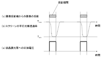
- FIG. 1 is a diagram showing the relationship between the waveform applied to the display of the present invention and the response waveform of the screen.
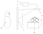
- FIG. 2 is a diagram illustrating a configuration example of the display device of the present invention.
- FIG. 3 shows an example of the timing at which the image projector projects an image on the screen (the projection of the image starts from the moment when the screen starts switching from the light transmission state to the light scattering state, and the screen completely moves from the light scattering state.
- FIG. 6 is a diagram showing (at the moment when the switching to the light transmission state is completed, the projection of the image is finished).
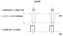
- FIG. 4 is a diagram illustrating an example of the timing at which the image projector projects an image on the screen (the period during which a voltage is applied to the liquid crystal light control layer coincides with the period during which an image is projected from the image projector).
- FIG. 5 is a diagram illustrating an example of the timing at which the image projector projects an image on the screen (projecting an image from the image projector during a period in which the parallel light transmittance of the screen is the minimum T min ).
- FIG. 6 is a diagram illustrating an example of the relationship between the applied waveform and the response waveform of the screen according to the present invention.
- FIG. 7 is a diagram illustrating an example of the configuration of the image display apparatus according to the present invention in the fourth embodiment.
- FIG. 8 is a radiance spectrum diagram of the screen portion of the image display device according to the fourth embodiment.
- the description of the constituent requirements described below is an example (representative example) of an embodiment of the present invention, and is not specified by these contents.
- the image display apparatus according to the present invention includes a screen and an image projector for projecting an image onto the screen, and at least one screen is disposed with respect to the image projector.
- the screen of the present invention can be switched between a light transmission state and a light scattering state.
- the image projector is one of the screens.
- An image is projected onto a part or the whole, and the screen and the image projector are synchronized so that the image projector does not project an image when the screen is in a light transmitting state.
- this synchronization switching at a speed that cannot be followed by the human eye, when the image is projected onto the screen, the image appears to be raised.
- light refers to visible light (wavelength 380 to 800 nm).
- the screen used in the present invention is a screen that can be switched to a light scattering state by applying a voltage in a light transmitting state when no voltage is applied.
- the screen of the present invention is transparent in normal use (no voltage applied) in applications such as windows and showcases, and can display an image in a light scattering state when a voltage is applied.
- the screen includes a transparent substrate, at least one of which is included in the screen, and a pair of substrates with electrodes disposed to face each other, and a dielectric anisotropy is positive between the pair of substrates with electrodes. It has a liquid crystal light control layer containing a composite containing a certain chiral nematic liquid crystal phase and a polymer resin phase.
- Switching between the light transmission state and the light scattering state can be realized by electrically driving the liquid crystal light control layer.
- the liquid crystal light control layer a composite of a transmission-scattering liquid crystal phase and a polymer resin phase that can be switched between a light transmission state and a light scattering state by electric drive can be used.
- the liquid crystal light control layer used in the present invention is in a light transmissive state when no voltage is applied, and is switched to a light scattering state by a DC voltage, an AC voltage, a pulse voltage, or a combination thereof having an effective value equal to or greater than a threshold value.
- the liquid crystal light control layer may be a reverse mode drive that returns to a light transmissive state when the applied voltage is removed, or a memory mode drive that applies a voltage only when switching between the light transmissive state and the light scattering state.
- a thing may be used.
- the screen of the present invention has a high contrast between the light transmission state and the light scattering state, so that a clear image can be displayed without particularly increasing the light source of the image projector.
- the screen is driven such that the light transmitting state and the light scattering state are periodically switched, and the frequency is 40 Hz or more and 100 Hz or less.
- the light scattering state in the present invention refers to a state where the parallel light transmittance is less than 30%, and the light transmissive state in the present invention refers to a state where the parallel light transmittance is 80% or more.
- a state in which the screen is driven by periodically switching between a light transmission state and a light scattering state may be expressed as a display mode.
- the normal cycle drive means that the drive is performed exactly the same every cycle. However, a different drive may be included as long as it does not depart from the spirit of the present invention.
- the periodic switching between the light transmission state and the light scattering state of the screen used in the present invention has a frequency of 40 Hz or more, preferably 45 Hz or more, 100 Hz or less, preferably 70 Hz or less, more preferably 60 Hz or less. When the frequency is lower than 40 Hz, flickering occurs on the screen in the display mode.
- the duty ratio of the periodic switching of the screen used in the present invention is 0.01 or more and 0.20 or less.
- the duty ratio of the screen is a ratio of time in the light scattering state in the periodic switching between the light transmitting state and the light scattering state.
- the duty ratio of the periodic switching of the screen of the present invention is 0.01 or more, preferably 0.05 or more, while the upper limit is 0.20 or less, preferably 0.15 or less.
- the smaller the duty ratio the smaller the haze of the screen in the display mode, and the background transparency is improved.
- the duty ratio is 0.20 or less, when an image is displayed in the display mode, the background can be seen well even in a dark place such as a room.
- the larger the duty ratio the clearer the displayed image.
- both video visibility and background transparency can be achieved.
- the parallel light transmittance and tau ON of less than 30% of the time ⁇ ON / ( ⁇ ON + ⁇ OFF)
- ⁇ ON / ( ⁇ ON + ⁇ OFF) is preferably 0.01 or more, and more preferably 0.05 or more.
- it is preferably 0.20 or less, and more preferably 0.15 or less.
- the instantaneous parallel light transmittance can be measured by using a commercially available high-speed compatible spectrometer, high-speed compatible luminance meter, or the like.
- the duty ratio of the pulse voltage having an effective value exceeding the threshold of the liquid crystal light control layer is 0.01 to 0.20 in the liquid crystal light control layer having a frequency of 40 Hz to 100 Hz. This can be realized by applying a burst voltage (hereinafter, it may be expressed as a pulse voltage or a burst voltage).
- the parallel light transmittance when a voltage is applied to the liquid crystal light control layer of the screen, it takes a finite time for the parallel light transmittance to be reduced when switching to the light scattering state, while on the other hand, It also takes a finite time for the parallel light transmittance to increase. Due to the presence of these transient states in which the parallel light transmittance fluctuates with time, the parallel light transmittance at the timing when the parallel light transmittance is low or the light scattering state is originally desired at the timing when the light is desired to be in the light scattering state. Inconvenience that the display mode is high, and as a result, the transparency of the display mode is reduced and the visibility of the display image is lowered.
- both the rising response time ⁇ 1 and the falling response time ⁇ 2 are 3.0 ms or less. More preferably, both are 2.0 ms or less.
- the parallel light transmittance of the screen is preferably less than 30% and more preferably less than 20% during the period in which the image projector projects an image. It is. In other periods, the higher the parallel light transmittance of the screen is, the better, and preferably 80% or more. On the other hand, in the transient state where the parallel light transmittance of the screen is 30% or more and less than 80%, sufficient visibility is not obtained even when the image is projected, but the transparency is low. is there.
- this transient state can be shortened, so that both the visibility of the image and the transparency of the background can be achieved. Further, it is preferable that the values of ⁇ 1 and ⁇ 2 are the same or approximate values because synchronization control is facilitated.
- the haze of the light scattering state portion of the screen of the present invention is defined by the measuring method of JIS K7136 (2000).
- haze means what was measured as a time average.
- the radiance of the display image in the image display device of the present invention is calculated by integrating the spectral radiance measured in JIS Z8724 (1997) in the visible light wavelength region.
- the duty ratio of periodic switching By adjusting the duty ratio of periodic switching, it is possible to select whether to emphasize the background or the video. That is, by reducing the duty ratio of periodic switching, the haze of the screen in the display mode can be reduced, but the radiance of the display image is also reduced. Conversely, increasing the duty ratio of the periodic switching increases the haze of the screen in the display mode, but increases the radiance of the display image.
- the haze in the display mode when applying a burst voltage having a frequency of 40 Hz to 100 Hz and a duty ratio of 0.01 to 0.20 is preferably 20% or less, and 15% or less. Is more preferable. Moreover, 1% or more is preferable and 5% or more is still more preferable. If the haze is not too large, the background transparency tends to be good, and if it is not too small, the brightness of the display image tends to be ensured to be visible.
- the positional relationship between the screen and the image projector in the present invention may be a rear projection system in which the viewer and the image projector face each other with the screen interposed therebetween, or a front projection system in which the viewer and the image projector are on the same side with respect to the screen.
- the former may be used when back scattering is strong, and the latter may be used when forward scattering is strong.
- You may install so that the light emission port of an image projector may become perpendicular
- the contrast of the display image is calculated by (white display radiance) / (black display radiance).
- the luminance ratio is preferably a specific value in the incident direction of the specific range of the image.
- the image projector projects an image on a part or the whole of the screen, and when the screen is in a light transmission state, the image projector Synchronize so that the image is not projected.
- the screen is driven so that the light transmission state and the light scattering state of the screen are periodically switched.
- the ratio of the radiance of white display to black display is 30 or more when the incident direction of the image projected from the image projector is within 30 ° with respect to the screen. Furthermore, it is preferable that it is 60 or more.
- the liquid crystal light control layer of the screen used in the present invention scatters light by a composite structure of a focal conic phase of chiral nematic liquid crystal and a network polymer.
- the focal conic phase which is a random liquid crystal polydomain structure, and a random network polymer structure, incident light is scattered over a wide range and a wide viewing angle is given. Even when viewed, the visibility of the image is improved.
- the screen of the present invention is in a light transmission state when no voltage is applied, and the haze at this time is preferably 10% or less. Further, it is preferably 8% or less, particularly preferably 5% or less. Moreover, it becomes a light-scattering state at the time of voltage application, and it is preferable that haze switches to 85% or more by applying the continuous wave of a DC voltage or an AC voltage to a screen, and it is preferable to become 90% or more.
- the upper limit is 100%, and the higher the better. Within these ranges, the visibility of the displayed image tends to be good.
- the upper limit of the operating temperature of the screen of the present invention is the liquid crystal-isotropic phase transition temperature (Tni) of the chiral nematic liquid crystal phase, but the response time tends to be longer at low temperatures. Therefore, the operating temperature range is preferably ⁇ 10 ° C. or higher, more preferably 0 ° C. or higher. Moreover, it is preferably 60 ° C. or lower, and more preferably 40 ° C. or lower.
- the screen of the present invention has a chiral substrate having at least one transparent substrate and a pair of substrates with electrodes disposed opposite to each other, and positive dielectric anisotropy between the pair of substrates with electrodes.
- a liquid crystal light control layer including a composite including a nematic liquid crystal phase and a polymer resin phase is included.
- the liquid crystal light control layer used for the screen of the present invention includes a composite containing a chiral nematic liquid crystal phase having a positive dielectric anisotropy and a polymer resin phase. This scheme is known as PSCT.
- PSCT the drive mode of the reverse mode PSCT will be described.
- reverse mode PSCT when no voltage is applied, almost all of the liquid crystal helical axes are in a planar phase facing the direction perpendicular to the substrate and take a light transmission state.
- the liquid crystal helical axis undergoes a phase transition to a focal conic phase in a random direction, resulting in a light scattering state.
- the parallel light transmittance of the screen can be controlled.
- the liquid crystal molecule major axis undergoes phase transition to a homeotropic phase in a direction perpendicular to the substrate, resulting in a light transmission state.
- the chiral nematic liquid crystal used in the screen of the present invention has a positive dielectric anisotropy. Since the dielectric anisotropy of the chiral nematic liquid crystal of the present invention is positive, both a decrease in T min and a decrease in ⁇ 1 and ⁇ 2 can be achieved.
- the dielectric anisotropy value ( ⁇ ) of the chiral nematic liquid crystal is not particularly limited as long as it is positive, but is preferably 5 or more, and more preferably 8 or more for reducing the driving voltage of the screen.
- numerator which comprises a chiral nematic liquid crystal does not have absorption of the wavelength which overlaps with the absorption wavelength of an initiator.
- the liquid crystal itself may be an assembly of liquid crystalline compounds exhibiting a cholesteric phase, or a chiral nematic liquid crystal may be formed by adding a chiral agent to the nematic liquid crystal. From the viewpoint of designing the liquid crystal composition, it is preferable to add a chiral agent to the nematic liquid crystal according to the purpose and control the chiral pitch length (p) and the liquid crystal-isotropic phase transition temperature (Tni).
- d / p is 1 or more, where d is the distance between the substrates with electrodes and p is the chiral pitch length of the chiral nematic liquid crystal.
- d / p is more preferably 2 or more, and still more preferably 4 or more. Further, d / p is preferably 20 or less, and particularly preferably 12 or less.
- the threshold voltage from the focal conic phase to the homeotropic phase is increased, and even when a high voltage is applied, the light transmission state is not changed and the light scattering state can be maintained. Therefore, the rising response time ⁇ 1 can be shortened.
- the screen drive voltage threshold voltage from the planar phase to the focal conic phase
- the chiral pitch length p of the chiral nematic liquid crystal is preferably 0.3 ⁇ m or more, and more preferably 0.8 ⁇ m or more.
- the chiral pitch length p is preferably 3 ⁇ m or less, more preferably 2 ⁇ m or less. If the chiral pitch length p is not too small, the screen drive voltage tends to be kept low, and if it is not too large, the contrast tends to be high. Since p is generally inversely proportional to the concentration of the chiral agent, the concentration of the chiral agent may be determined by calculating backward from the value of the required chiral pitch length p.
- the screen finally obtained is colored when no voltage is applied, and is out of the visible light range. In some cases, it becomes colorless and transparent when no voltage is applied, so the chiral pitch length p may be selected according to the purpose.
- the distance d between the substrates with electrodes of the screen of the present invention needs to be not less than the chiral pitch length p of the chiral nematic liquid crystal to be used, and is usually preferably 3 ⁇ m or more, more preferably 5 ⁇ m or more.
- the distance d is preferably 100 ⁇ m or less, and more preferably 20 ⁇ m or less.
- the light transmittance of the screen when no voltage is applied decreases as the distance d increases, and the response time of the display may become longer.
- d is too small, the light-shielding characteristic during driving is reduced, and in the case of a large area screen, the screen may be short-circuited. By being in the above range, these requirements can be satisfied in a balanced manner.
- Tni of the chiral nematic liquid crystal is preferably 50 ° C. or higher, and more preferably 70 ° C. or higher, because the upper temperature limit at which the screen can operate is determined by Tni of the chiral nematic liquid crystal.
- Tni increases, the viscosity tends to increase, so that it is preferably 200 ° C. or lower, and more preferably 150 ° C. or lower.
- the nematic liquid crystal may be any known one, and the molecular skeleton, substituent, and molecular weight of the constituent molecules are not particularly limited, and may be a synthetic product or a commercial product.
- the dielectric anisotropy of the nematic liquid crystal is preferably positive and large in order to make the dielectric anisotropy of the chiral nematic liquid crystal phase of the screen and the chiral nematic liquid crystal of the liquid crystal composition positive.
- a polymerization initiator it is preferable from the viewpoint of shortening the curing time of the polymerizable monomer that each molecule constituting the constituent molecule does not have absorption at a wavelength overlapping the absorption wavelength of the initiator.
- the chiral agent may be any chiral compound that is compatible with the host liquid crystal, may be a synthetic product or a commercial product, may exhibit liquid crystal properties, or may have a polymerizable functional group. Good. Further, dextrorotatory or levorotatory may be used, and a dextrorotatory chiral agent and a levorotatory chiral agent may be used in combination.
- the chiral agent those having a large dielectric anisotropy per se and a low viscosity are preferable from the viewpoints of reduction in driving voltage and response speed of the screen, and the helical agent is an index of the force for twisting the liquid crystal. A larger Twisting Power is preferable.
- the polymerization initiator does not have absorption at a wavelength that overlaps the absorption wavelength of the initiator.
- Examples of the chiral agent include CB15 (trade name, manufactured by Merck), C15 (trade name, manufactured by Merck), S-811 (trade name, manufactured by Merck), R-811 (trade name, manufactured by Merck), S-1011 (trade name, manufactured by Merck), R-1011 (trade name, manufactured by Merck) and the like.
- the polymer resin phase of the present invention is preferably formed by curing a specific polymer precursor.
- the polymer resin phase of the present invention is preferably 10% by mass or less, and more preferably 7% by mass or less, with respect to the chiral nematic liquid crystal phase. Moreover, it is preferable that it is 0.1 mass% or more, and it is preferable that it is 1 mass% or more.
- the ratio of the polymer resin phase is not too small, the polymer resin phase becomes mechanically tough and tends to be excellent in repeated durability.
- the liquid crystal molecules can receive sufficient interface interaction, the contrast and response speed of the screen may be increased.
- the ratio of the polymer resin phase is not too large, an increase in driving voltage is suppressed and the transparency of the screen tends to be high.
- the polymer resin used in the polymer resin phase of the present invention is not particularly limited as long as the effects of the present invention are not impaired, but is obtained by curing a mixture containing a polymer precursor represented by the following general formula (1). Is preferably used because it tends to achieve both a reduction in the minimum parallel light transmittance T min when a screen voltage is applied and a shortening of ⁇ 1 and ⁇ 2 .
- a 1 and A 2 each independently represent a hydrogen atom or a methyl group
- Ar 1 , Ar 2 and Ar 3 each independently represent a divalent aromatic hydrocarbon ring group which may have a substituent or a divalent aromatic heterocyclic group which may have a substituent.
- X 1 and X 2 are each independently a direct bond, a carbon double bond, a carbon triple bond, an ether bond, an ester bond, a linear alkylene group having 1 to 6 carbon atoms which may have a substituent, or a substituent.
- R 1 and R 2 are each independently a linear alkylene group having 1 to 6 carbon atoms which may have a substituent, or a linear chain having 1 to 6 carbon atoms which may have a substituent.
- at least one of Ar 1 , Ar 2 and Ar 3 is a divalent aromatic condensed ring group which may have a substituent or a divalent aromatic which may have a substituent.
- the divalent aromatic hydrocarbon ring group which may have a substituent for Ar 1 , Ar 2 and Ar 3 is not particularly limited as long as it does not impair the effects of the present invention.
- the hydrocarbon ring group is a divalent group obtained by removing two hydrogen atoms from a single ring or a condensed ring formed by condensation of 2 to 4 thereof. Specific examples include a benzene ring and a naphthalene ring.
- the number of carbon atoms is preferably 6 or more, and on the other hand, it is preferably 30 or less, more preferably 26 or less, and particularly preferably 18 or less from the viewpoint of curability during polymerization. Specific examples include the following structures.
- the divalent aromatic hydrocarbon ring group which may have a substituent of Ar 1 , Ar 2 and Ar 3 has the following structure in particular, and the curability of the polymer precursor is high. preferable.
- Examples of the substituent that the divalent aromatic hydrocarbon ring group of Ar 1 , Ar 2 and Ar 3 may have include a fluorine atom, a chlorine atom, a hydroxyl group, a cyano group, a methyl group, an ethyl group, n- Propyl group, isopropyl group, methoxy group, ethoxy group, n-propoxy group, isopropoxy group, n-butyl group, isobutyl group, t-butyl group and the like can be mentioned.
- the divalent aromatic heterocyclic group which may have a substituent for Ar 1 , Ar 2 and Ar 3 is not particularly limited as long as it does not impair the effects of the present invention.
- the number of carbon atoms is preferably 6 or more, and on the other hand, it is preferably 30 or less, more preferably 26 or less, and particularly preferably 18 or less from the viewpoint of curability during polymerization.
- Specific examples include the following structures.
- the divalent aromatic heterocyclic group which may have a substituent of Ar 1 , Ar 2 and Ar 3 , the following structure is particularly preferable among the above, since the curability of the polymer precursor is high. .
- Examples of the substituent that the divalent aromatic heterocyclic group represented by Ar 1 , Ar 2 and Ar 3 may have include a fluorine atom, a chlorine atom, a hydroxyl group, a cyano group, a methyl group, an ethyl group, and n-propyl.
- X 1 and X 2 are each independently a direct bond, a carbon double bond, a carbon triple bond, an ether bond, an ester bond, a linear alkylene group having 1 to 6 carbon atoms which may have a substituent, or a substituent.
- a straight-chain oxyalkylene group having 1 to 6 carbon atoms which may have a group, preferably a direct bond, an ether bond, an ester bond or a methylene group.
- the substituents that may be included are fluorine atom, chlorine atom, hydroxyl group, cyano group, methyl group, ethyl group, n-propyl group, isopropyl group, methoxy group, ethoxy group, n-propoxy group, isopropoxy group Group, n-butyl group, isobutyl group, t-butyl group and the like, preferably fluorine atom, hydroxyl group, cyano group, methyl group and methoxy group.
- R 1 and R 2 are each independently a linear alkylene group having 1 to 6 carbon atoms which may have a substituent, or a linear chain having 1 to 6 carbon atoms which may have a substituent.
- An oxyalkylene group or a linear alkyl ester group having 2 to 6 carbon atoms is represented.
- the straight chain alkyl ester group having 2 to 6 carbon atoms represents, for example, the following structure.
- R 1 and R 2 may have include a fluorine atom, chlorine atom, hydroxyl group, cyano group, methyl group, ethyl group, n-propyl group, isopropyl group, methoxy group, ethoxy group, n -Propoxy group, isopropoxy group, n-butyl group, isobutyl group, t-butyl group and the like are mentioned, and preferred are fluorine atom, hydroxyl group, cyano group, methyl group and methoxy group.
- At least one of Ar 1 , Ar 2 and Ar 3 is a divalent aromatic condensed ring group which may have a substituent or a divalent aromatic heterocyclic ring which may have a substituent. It is a group.
- a divalent aromatic condensed ring group which may have a substituent or a divalent aromatic heterocyclic group which may have a substituent in the molecule the rigidity of the polymer resin phase after curing Tends to shorten ⁇ 1 and ⁇ 2, which is preferable.
- the polymer precursor represented by the general formula (1) is a polymer precursor represented by the following general formula (2).
- a 1 and A 2 each independently represent a hydrogen atom or a methyl group
- Ar 4 represents a divalent aromatic hydrocarbon condensed ring group which may have a substituent or a divalent hetero condensed ring group which may have a substituent
- R 1 and R 2 each independently represents an alkylene group having 2 to 6 carbon atoms which may have a substituent
- p and q each independently represents 0 or 1.
- Specific examples of the divalent aromatic hydrocarbon ring group that may have a substituent of Ar 4 and the divalent heterocyclic group that may have a substituent include those listed for Ar 1. It is synonymous and the substituent which you may have is also synonymous. Among these, the structure represented below is preferable because the curability of the polymer precursor is increased.
- Ar 4 is preferably a divalent aromatic hydrocarbon condensed ring group which may have a substituent because the mechanical strength of the polymer resin phase is increased, and among them, the number of carbon atoms is 6
- the molecular size is too large, the degree of spatial freedom for the polymer precursor to undergo a polymerization reaction is reduced, and the polymerization reaction does not occur sufficiently. In particular, it is preferably 18 or less.
- Ar 4 is preferably a divalent benzene ring which may have a substituent or a divalent naphthalene ring which may have a substituent among the above, and has a substituent. A good divalent naphthalene ring is particularly preferable because of high curability of the polymer precursor.
- Ar 4 has a strong electron donating property to the polymerizable group.
- the position at which Ar 4 is bonded to —O— is not particularly limited, but the molecule preferably has a linear structure.
- the benzene ring is bonded to the 1,4-position, and the naphthalene ring monocycle is bonded to the 1,4-position or the 2,6-position.
- the polymer precursor used in the liquid crystal light control layer of the present invention only one kind of polymer precursor represented by the above formula (1) may be used, or two or more kinds may be used in combination.
- the ratio of the polymer precursor represented by the general formula (1) used for the screen of the present invention and the other polymer precursor is not particularly limited as long as the effects of the present invention are not impaired, but the general formula (1) ) Is preferably 30% by mass or more, more preferably 50% by mass or more, and most preferably 80% by mass or more.
- the proportion of the polymer precursor represented by the above formula (1) is too small, one of screen production in a short time, high contrast, short response time, or a plurality of the precursors may not be sufficient.
- the upper limit of the polymer precursor represented by the above formula (1) is 100% by mass.
- the chiral nematic liquid crystal phase of the screen of the present invention has a polymerization initiator, a light stabilizer, an antioxidant, a thickener, a polymerization inhibitor, a photosensitizer, an adhesive, an antifoaming agent, a surfactant and the like. You may do it.
- content of the said other component can be mix
- the curing method of the polymer precursor may be either photocuring or heat curing, but photocuring is preferable, and among the photocuring, curing with ultraviolet rays or near ultraviolet rays is particularly preferable.
- the light source for photopolymerization may be any light source having a spectrum at the absorption wavelength of the radical photopolymerization initiator used, and typically any light source capable of irradiating light with a wavelength of 220 nm to 450 nm. . Examples include high pressure mercury lamps, ultra high pressure mercury lamps, halogen lamps, metal halide lamps, UV-LEDs (Light Emitting Diodes), blue LEDs, white LEDs, and the like.
- a heat ray cut filter an ultraviolet ray cut filter, a visible light cut filter, or the like may be used in combination.
- Light may be applied to at least one surface from the transparent substrate of the screen, and if both surfaces of the substrate sandwiching the liquid crystal composition are transparent, both surfaces may be irradiated with light. Light irradiation may be performed at one time or may be performed by dividing into several times. So-called PSCOF (Phase Separated Composite Organic Film) (V. Vorflusev and S. Kumar, Science 283, which distributes the irradiance of light in the thickness direction of the screen and continuously changes the density of the polymer resin phase. 1903 (1999)).
- PSCOF Phase Separated Composite Organic Film
- the irradiance of the light irradiated on the screen typically 0.01 mW / cm 2 or more, preferably 1 mW / cm 2 or more, more preferably 10 mW / cm 2 or more, particularly preferably 30 mW / cm 2 That's it. If the irradiance is too small, the polymerization does not proceed sufficiently. Further, for photocuring of the liquid crystal composition, an integrated irradiation amount of usually 2 J / cm 2 or more, preferably 3 J / cm 2 or more may be given, and the light irradiation time may be determined according to the radiation intensity of the light source.
- the light irradiation is usually completed within 200 seconds, preferably within 60 seconds, while it is preferable to perform light irradiation for 10 seconds or more. If the light irradiation time is too short, the repetition durability of the screen may be inferior.
- the chiral nematic liquid crystal is dispersed or formed into a continuous layer in a thin transparent polymer, but the continuous layer exhibits the best contrast. Is formed.
- the screen used in the present invention is a transparent substrate at least one of which includes a pair of substrates with electrodes arranged opposite to each other, and a liquid crystal light control layer including a composite of a chiral nematic liquid crystal and a polymer resin between the substrates,
- the liquid crystal light control layer is obtained by curing a liquid crystal composition composed of a polymerizable monomer and a chiral nematic liquid crystal.
- the screen used in the present invention is not particularly limited as long as it is the above-mentioned screen, but a typical structure will be described below.
- At least one of the substrates is transparent, and preferably both are transparent.
- the material of the substrate include colorless transparent or colored transparent or opaque materials such as inorganic transparent materials such as glass and quartz, metals, metal oxides, semiconductors, ceramics, plastic plates, and plastic films.
- a thin film of metal oxide, metal, semiconductor, organic conductive material or the like is formed on the entire surface of the substrate or partially by a known coating method, printing method, vapor deposition method such as sputtering, or the like. is there. Alternatively, it may be partially etched after forming a conductive thin film.
- an ITO (mixture of indium oxide and tin oxide) electrode is deposited on a transparent polymer film such as PET or PEN, or a deposition method or printing method such as sputtering. It is desirable to use an electrode substrate formed by using, for example. A wiring for connecting the electrodes or connecting the electrodes and the outside may be provided on the substrate. For example, a segment driving electrode substrate, a matrix driving electrode substrate, an active matrix driving electrode substrate, or the like may be used.
- a strip-shaped electrode can be formed on one substrate in the direction of the short side of the strip, and a solid electrode can be used on the other to form a strip-shaped segment.
- a strip-shaped electrode can be used to form a matrix-like segment so that the strips face each other so as to be orthogonal.
- the electrode surface provided on the substrate is a protective film made of an organic compound such as polyimide, polyamide, polyvinyl alcohol, silicon, and cyanide, an inorganic compound such as SiO 2 , TiO 2 , and ZrO 2 , or a mixture thereof.
- the entire surface or a part thereof may be covered with an alignment film.
- the substrate may be aligned so that the liquid crystal is aligned with respect to the surface of the substrate. When the alignment is processed, any alignment processing can be used as long as the chiral nematic liquid crystal in contact has a planar structure. It doesn't matter.
- the two substrates may be homogeneously aligned, or may be a so-called hybrid in which one is homogeneously aligned and the other is homeotropic aligned.
- the electrode surface may be directly rubbed, or a normal alignment film such as polyimide used for TN (Twisted Nematic) liquid crystal, STN (Supper Twisted Nematic) liquid crystal, or the like may be used.
- a so-called photo-alignment method may be used in which the organic thin film on the substrate is irradiated with light having anisotropy such as linearly polarized light to give the film anisotropy.
- the polymer resin phase contained in the liquid crystal light control layer may have an alignment film function.
- the opposing substrate may have an adhesive layer including a resin body for adhering and supporting the substrate as appropriate at the periphery.
- the end face of the screen or the liquid crystal injection port used in the present invention is a tape such as an adhesive tape, a thermocompression bonding tape, a thermosetting tape, and / or a thermosetting resin, a photocurable resin, a moisture curable resin.
- Curable resins such as room temperature curable adhesives, anaerobic adhesives, epoxy adhesives, silicone adhesives, fluororesin adhesives, polyester adhesives, vinyl chloride adhesives, and thermoplastic resins
- This sealing may also work to prevent deterioration of the screen at the same time.
- the end face may be protected by covering the entire end face, or by pouring curable resins or thermoplastic resins into the screen from the end face and solidifying it. It may be covered with a kind.
- Spacers such as spherical or cylindrical glass, plastic, ceramic, or plastic film may be present between the substrates arranged to face each other.
- the spacer may be dispersed in the liquid crystal composition, or may be fixed in the liquid crystal light control layer between the substrates.
- the spacer may be dispersed on the substrate during screen assembly or mixed with an adhesive to bond the adhesive layer.
- the liquid crystal light control layer included in the screen used in the present invention is, for example, a sealing cell by forming an adhesive layer with a photo-curing adhesive or the like on a peripheral portion of a pair of electrodes facing each other via a spacer, Inject or inject liquid crystal composition in normal pressure or vacuum in the notch of one or more adhesive layers provided in advance, or apply the liquid crystal composition on one substrate using a coater, and After being sandwiched by a known method such as stacking the other substrate, it is formed by polymerization and curing by radiation such as ultraviolet light, visible light, or electron beam.
- a substrate with electrodes supplied continuously can be sandwiched between two rolls and the like, and a liquid crystal composition containing and dispersed a spacer can be fed between them, and then it can be photocured continuously. So productivity is high.
- At least one surface or both surfaces of the screen may be covered with an antireflection film, an antiglare film, an ultraviolet blocking film, or an antifouling film. For example, by covering the front and back of the screen with an antireflection film, reflection of external light on the substrate surface is prevented, and the appearance of the screen is improved.
- the image projector used in the present invention may be any one that can project an image in a time division manner, and includes, for example, a configuration in which a shutter is provided between a light source and a screen.
- a shutter a liquid crystal light valve or the like can be used in addition to a general mechanical shutter.
- a ferroelectric liquid crystal or a liquid crystal light valve using a transmission / scattering type liquid crystal mode may be used.
- a polarizing plate it is preferable that the polarization of the light emitted from the image projection device of the projector is aligned with the transmission axis of the light incident side polarizing plate of the shutter because the light use efficiency is increased.
- the projection timing of the image from the image projection apparatus may be directly synchronized with the driving timing at which the liquid crystal layer of the screen takes the light transmission state and the light scattering state.
- the light source may be turned on / off instead of the shutter.
- an LED capable of high-speed switching may be used as the light source.
- the image projector a commercially available liquid crystal projector, CRT (Cathode Ray Tube) projector, LED projector, laser projector, or the like can be used.
- a light source such as a lamp, LED, OLED, or laser may be used to modulate light with a light valve, a color filter, a mirror, or the like.
- a control device that controls the timing of projecting an image, it is preferable to use the control device in combination.
- At least one screen is disposed with respect to the image projector, and when the screen is in the light scattering state or while the light transmission state is changed to the light scattering state, the image projector is An image is projected onto a part or the whole of the screen, and is synchronized so that the image projector does not project an image when the screen is in a light transmitting state.
- FIG. 2 shows a configuration example of the display device of the present invention.
- Reference numeral 1 denotes a display screen, which is a rear projection system in which the image projector 2 and the observer O face each other.
- the observer O can see the background B (product) through the display screen 1.
- the display screen 1 and the image projector 2 are controlled in drive timing by a signal transmitted from the control device 3.
- the image display device of the present invention includes a control device.
- the control device performs control to periodically switch between the light transmission state and the light scattering state of the screen.
- FIGS. 3, 4, and 5 respectively show (a) voltage applied to the liquid crystal light control layer of the screen, (b) parallel light transmittance of the screen, and (c) image projection of the image projector.
- a time chart is shown.
- FIG. 3 shows an example in which the projection of an image starts from the moment when the screen starts to switch from the light transmission state to the light scattering state, and the projection of the image ends at the moment when the screen ends from the light scattering state to the completely light transmission state. Show. In this case, the period during which the parallel light transmittance of the screen is smaller than T min, the image projector is that it is projecting an image.
- T min the period during which the parallel light transmittance of the screen is smaller than T min
- FIG. 4 shows a case where the period during which the voltage is applied to the liquid crystal light control layer and the period during which the image is projected from the image projector are matched.
- FIG. 5 shows a case where an image is projected from the image projector during a period in which the parallel light transmittance of the screen is the minimum T min .
- T min is preferably 30% or less.
- One image projector may be arranged on one screen, or two or more image projectors may be arranged on one screen. When two or more image projectors are arranged on one screen, the image may be projected on the same place on the screen, or the image may be projected on different places.
- Two or more screens may be arranged for one image projector. When two or more screens are arranged for one image projector, they can be arranged in a plane or in the depth direction.
- the image may be projected on only one segment, the image may be projected on two or more, or all segments .
- all the display areas may be synchronously driven at the same timing, or synchronously driven at different timings for each screen or segment. Also good. In the latter case, the visibility of the image can be improved by sequentially switching the image projection for each screen or segment and setting so that the image is always projected in any one of the display areas. For example, when the screen is divided into N segments, assuming that the frequency for periodically driving the screen is F (Hz), the duty ratio of the light scattering state per segment is set to 1 / N, and 1 is set for adjacent segments.
- the screen segments are arranged in strips, the segments are arranged in the short side direction, the scan lines are aligned with the long side directions, and the sub-scan lines are It can be matched with the long side direction of the segment.
- a light beam scanning method any of a raster scan method, a vector scan method, and an interlace method may be used.
- an image projector that draws an image by scanning a light beam an image projector using a laser as a light source is preferable in terms of high color reproducibility of an image and a small image projector.
- the response time of the screen was measured at room temperature of 25 ° C.
- a halogen lamp was used as the light source, and light was incident on the screen vertically while applying a predetermined burst voltage.
- the brightness L of the element transmitted light was measured using a multimedia display tester 3298F (manufactured by YOKOGAWA) as a detector.
- a digital oscilloscope was used to monitor the applied waveform and response waveform.
- the parallel light transmittance T (%) of the element was calculated by L / L 0 ⁇ 100 based on the brightness L 0 of the blank.
- T max the minimum value of the parallel light transmittance when voltage is applied
- T min the pulse voltage application start time
- t 2 the application end time
- ⁇ 1 the time until the parallel light transmittance reaches T 10 for the first time from t 1
- ⁇ 2 the parallel light transmission for the first time from t 2.
- the rate is the time to reach the T 90.
- T 10 0.1 ⁇ (T max ⁇ T min )
- T 90 0.9 ⁇ (T max ⁇ T min )
- the relationship between the applied waveform and the response waveform of the screen is shown in FIG.
- Applied waveform using a burst waveform as in FIG. 6, was applied by setting the frequency F and duty ratio D V to a predetermined value.
- the pulse amplitude V was 100 Vp-p.
- ⁇ ON the time when the parallel light transmittance of the screen is 30% or less
- ⁇ OFF the time when the screen is less than 30%
- ⁇ ⁇ 1 ⁇ 2 .
- ⁇ 1 is the dielectric constant in the major axis direction of the liquid crystal molecules
- ⁇ 2 is the dielectric constant in the uniaxial direction of the liquid crystal molecules.
- D represents the thickness of the liquid crystal layer.
- S represents the overlapping portion of the electrodes of the two electrode substrates. It represents the area of).
- Chiral nematic liquid crystal (a) 95.0 wt%, monomer represented by the following structural formula (II) (Ac-N, trade name, manufactured by Kawasaki Kasei Co., Ltd.) 2.4 wt%, represented by the following structural formula (III) Monomer (Mc-N, trade name, manufactured by Kawasaki Kasei Co., Ltd.) 2.4 wt% and polymerization initiator represented by the following structural formula (IV) (Lucirin TPO, trade name, manufactured by BASF JAPAN) 0.2 wt% It mixed, stirred and filtered and the liquid-crystal composition (A) of Tni 94 degreeC was prepared.
- the cell was irradiated with UV light (wavelength 365 nm) on both sides at 1.6 J on one side at a room temperature at a room temperature to cure the monomer, and a screen (A-1) was obtained.
- the produced screen (A-1) had a transparent appearance, and showed reverse mode driving that changed to an opaque appearance when a voltage was applied.
- V (Vp-p) a rectangular wave of 100 Hz
- ultraviolet light wavelength 365 nm
- the produced screen (A-2) had a transparent appearance, and showed reverse mode driving that changed to an opaque appearance when a voltage was applied.
- V (Vp-p) a rectangular wave voltage
- the glass substrate used was a transparent electrode provided with an alignment film subjected to a homogeneous alignment treatment.
- the cell was irradiated with UV light (wavelength 365 nm) on both sides at a temperature of room temperature and 3.0 J on one side on both sides to cure the monomer to obtain a screen (B-1).
- the produced screen (B-1) had a transparent appearance, and showed a reverse mode drive that changed to an opaque appearance when a voltage was applied.
- V (Vp-p) a rectangular wave voltage
- a transparent electrode provided with an alignment film subjected to homeotropic alignment treatment was used.
- This cell was irradiated with ultraviolet light (wavelength 365 nm) on each side at a temperature of room temperature at a temperature of 3.0 J on both sides by 3.0 J to cure the monomer to obtain a screen (C-1).
- the produced screen (C-1) had a transparent appearance, and showed reverse mode driving that changed to an opaque appearance when a voltage was applied.
- V (Vp-p) a rectangular wave voltage
- Example 4 Using the screen (A-1) of Example 1, the image display device shown in FIG. 7 was produced.
- reference numeral 11 is a light source
- reference numeral 12 is a liquid crystal light valve
- reference numeral 13 is a lens
- reference numeral 14 is a light chopper
- reference numeral 15 is an image projector
- reference numeral 16 is a screen
- reference numeral 17 is an image display device
- reference numeral 18 is luminance. It is a total.
- Table 2 shows the screen optical characteristics (D, haze at OFF, ⁇ 1 , ⁇ 2 , T min ) and see-through display characteristics with respect to the voltage waveform parameters (V, D V , F) applied to the screen (A-1).
- Display haze radiance contrast, flicker
- “ ⁇ ” indicates that no flicker is seen, and “ ⁇ ” indicates that flicker is seen.
- the haze at the time of display was 10.2%, the background was not blurred, and was clearly visible.
- the radiance C / R was 127.9, and the image looked bright. Also, no flicker was seen on the screen.
- Example 5 and 6 Screen parameter of the voltage waveform (V, D V, F) a relative except for changing as described in Table 2, the parameters of the voltage waveform using the same image display apparatus as in Example 4 (V, D V, F )
- the optical characteristics (D, haze at OFF, ⁇ 1 , ⁇ 2 , T min ) and see-through display characteristics (haze at display, radiance contrast, flicker) were evaluated.
- D was in the range of 0.01 to 0.20.
- the haze at OFF was 10% or less.
- Both ⁇ 1 and ⁇ 2 were 3.0 msec or less.
- T min was 30% or less in all cases.
- the radiance C / R was 60 or more, and the image looked bright. Also, no flicker was seen on the screen.
- Example 7 to 11 Except that the screen is changed to the screen (A-2), it is driven using the same image display device as in Examples 4 to 6, and the optical characteristics of the screen with respect to the voltage waveform parameters (V, D V , F) ( D, haze at OFF, ⁇ 1 , ⁇ 2 , T min ) and see-through display characteristics (display haze, radiance contrast, flicker).
- Table 2 shows the parameters (V, D V , F) of the voltage waveform.
- D was in the range of 0.01 to 0.20.
- the haze at OFF was 10% or less.
- Both ⁇ 1 and ⁇ 2 were 3.0 msec or less.
- T min was 30% or less in all cases.
- the radiance C / R was 60 or more, and the image looked bright. Also, no flicker was seen on the screen.
- Example 12 to 14 Except that the screen is changed to the screen (B-1), driving is performed using the same image display apparatus as in Examples 4 to 6, and the optical characteristics of the screen with respect to the voltage waveform parameters (V, D V , F) ( D, haze at OFF, ⁇ 1 , ⁇ 2 , T min ) and see-through display characteristics (display haze, radiance contrast, flicker).
- the voltage waveform parameters (V, D V , F) are shown in Table 2.
- D was in the range of 0.01 to 0.20.
- the haze at OFF was 10% or less.
- Both ⁇ 1 and ⁇ 2 were 3.0 msec or less.
- T min was 30% or less in all cases.
- the radiance C / R was 60 or more, and the image looked bright. Also, no flicker was seen on the screen.
- ⁇ 2 was as slow as 10 msec or more.
- the haze at the time of display was 20% or more, the background was blurred, and it was not clearly visible.
- the radiance C / R was 60 or less, and the image did not appear bright. Also, the screen flickered.
- Display screen 2 Image projector 3 Control device 11
- Light source 12 Liquid crystal light valve 13
- Lens 14 Light chopper 15
- Image projector 16 Screen 17
- Image display device 18 Luminance meter O Observer B Background L Projection light
Landscapes
- Physics & Mathematics (AREA)
- Chemical & Material Sciences (AREA)
- Nonlinear Science (AREA)
- General Physics & Mathematics (AREA)
- Crystallography & Structural Chemistry (AREA)
- Optics & Photonics (AREA)
- Mathematical Physics (AREA)
- Engineering & Computer Science (AREA)
- Materials Engineering (AREA)
- Organic Chemistry (AREA)
- Dispersion Chemistry (AREA)
- Liquid Crystal (AREA)
- Overhead Projectors And Projection Screens (AREA)
- Transforming Electric Information Into Light Information (AREA)
Description
本発明は、スクリーンと画像投影機から構成される画像表示装置に関する。更に詳しくは、スクリーンが、光散乱状態である時に、前記画像投影機が前記スクリーンの一部または全体に対して画像を投影し、前記スクリーンが光透過状態の時に前記画像投影機による画像の投影を行わないように同期せしめた画像表示装置に関する。
近年、窓ガラスやフィルムなどの透明体に映像を写し、同時に非表示部の背景も見えるようにしたシースルーディスプレイの開発が進められている。
従来技術としては、透明LCD(Liquid Crystal Display)、透明OLED(Organic Light Emitting Diode)、透明PDP(Plasma Display Panel)といった、従来型のFPD(Flat Panel Display)部材を透明化することによりシースルー表示を行うディスプレイが知られている。しかしながら、これらのディスプレイは、非表示部の光線透過率が高いものでも50%程度であり、暗い場所では背景が見えないという問題がある。
従来技術としては、透明LCD(Liquid Crystal Display)、透明OLED(Organic Light Emitting Diode)、透明PDP(Plasma Display Panel)といった、従来型のFPD(Flat Panel Display)部材を透明化することによりシースルー表示を行うディスプレイが知られている。しかしながら、これらのディスプレイは、非表示部の光線透過率が高いものでも50%程度であり、暗い場所では背景が見えないという問題がある。
これに対し、透明体として光透過状態と光散乱状態を切り替え可能なスクリーンを使用し、スクリーンが光散乱状態の時にプロジェクターで投影した映像を結像させ、視認可能にするシースルー表示方法も知られている。特許文献1には、スクリーンの光透過状態と光散乱状態とを周期的に変化させ、プロジェクターでの映像投射をスクリーン変調に同期させる表示システムが開示されている。このシステムによると、1周期における、スクリーンが光散乱状態にある時間の割合を一定以下に設定することで、シースルー表示が可能になる。また、スクリーン変調の周波数を大きくすることで、表示画像のちらつきを感じないように設定できる。
この表示方法を用いることで、非表示部の光線透過率を50%より大きくすることが可能であり、これまでにない透明感のある映像を提供することができる。
光透過状態と光散乱状態を切り替え可能なスクリーンとしては、液晶と高分子樹脂の複合体を調光層に用いたものが知られており、Polymer Dispersed Liquid Crystals(PDLC)およびPolymer Stabilized Cholesteric Texture(PSCT)が知られている。このうちPDLCは可視光透過率の温度依存性が大きく、視野角依存性が大きい等の問題がある。一方、PSCTは、可視光透過率の温度依存性が小さく可視光透過率の視野角依存性も小さく、また素子の応答速度も速い利点を有しており、有望視されている。
光透過状態と光散乱状態を切り替え可能なスクリーンとしては、液晶と高分子樹脂の複合体を調光層に用いたものが知られており、Polymer Dispersed Liquid Crystals(PDLC)およびPolymer Stabilized Cholesteric Texture(PSCT)が知られている。このうちPDLCは可視光透過率の温度依存性が大きく、視野角依存性が大きい等の問題がある。一方、PSCTは、可視光透過率の温度依存性が小さく可視光透過率の視野角依存性も小さく、また素子の応答速度も速い利点を有しており、有望視されている。
特許文献1の表示方法では、周期駆動において、スクリーンの光散乱状態にある時間の割合を小さくすることで背景を十分視認できるようになるが、映像が薄くなってしまう。一方、スクリーンの光散乱状態にある時間の割合を大きくすることで映像が強調されるが、背景がぼやけてくる。すなわち、映像の視認性と背景の透過性はトレードオフの関係にある。背景の透過性を確保しながら明るくはっきりとした映像を表示するために、特許文献1には特に強い光源を用いることが示されている。しかし、この場合、大型のプロジェクターが必要になり、背景を見る際に視界を妨げる問題点がある。また、リアプロジェクション方式の場合は強い光を観察者に向けることになるので、スクリーン越しの光漏れにより不快感を生じることや、特にレーザープロジェクターを用いる場合には安全面で問題が生じる場合が考えられる。
本発明は、上記課題に鑑みてなされたものであって、特に強い光源を用いなくとも、非表示部分の透明性と投影映像の視認性を両立した画像表示装置を提供することを目的とするものである。
本発明者等は上記課題を解決すべく鋭意検討した結果、切り替えできるスクリーンと、前記スクリーンに画像を投影するための画像投影機から構成される画像表示装置において、特定のスクリーンを用い、さらにスクリーンと画像投影機による映像投影を特定の方法で同期させることで、特に強い光源を用いることなく非表示部分の透明性と投影映像の視認性を両立できることを見出し、本発明に到達した。
即ち、本発明の要旨は、以下に存する。
〔1〕少なくとも一つのスクリーンと、前記スクリーンに画像を投影するための画像投影機と、前記スクリーンの光透過状態と光散乱状態を周期的に切り替える制御装置とを備える画像表示装置であって、
前記スクリーンは、少なくとも一方が透明な透明基板と、対向して配置される一対の電極付き基板を有し、前記一対の電極付き基板の間に、誘電率異方性が正であるカイラルネマチック液晶相と高分子樹脂相を含む複合体を含む液晶調光層を有し、
前記スクリーンは、電圧無印加時に光透過状態で、電圧印加することで光散乱状態に切り替えできるスクリーンであり、
前記スクリーンが光散乱状態である時に、前記画像投影機が前記スクリーンの一部または全体に対して画像を投影し、前記スクリーンが光透過状態の時に前記画像投影機による画像の投影を行わないように同期せしめ、
前記制御装置は、前記切り替わりの周波数が40Hz以上100Hz以下であり、かつ周期的切り替わりにおける光散乱状態のデューティー比が0.01以上0.20以下となるように制御する
ことを特徴とする画像表示装置。
〔2〕前記周期的切り替わりにおいて、平行光線透過率が30%以上の時間をτOFF、平行光線透過率が30%未満の時間をτONとするとき、τON/(τON+τOFF)が0.01以上0.20以下となることを特徴とする前記〔1〕に記載の画像表示装置。
〔3〕前記スクリーンに、周波数が40Hz以上100Hz以下であり、かつデューティー比が0.01以上0.20以下のバースト電圧を印加したとき、スクリーンが光透過状態から光散乱状態へ変化し、さらに光透過状態に戻る過程において、該スクリーンの立ち上がりの応答時間τ1と立ち下がりの応答時間τ2が、いずれも3.0ms以下であることを特徴とする前記〔1〕又は〔2〕に記載の画像表示装置。
〔4〕前記スクリーンに、周波数が40Hz以上100Hz以下であり、かつデューティー比が0.01以上0.20以下のバースト電圧を印加した時の光散乱状態部分のヘイズが、20%以下であることを特徴とする前記〔1〕~〔3〕の何れか1つに記載の画像表示装置。
〔5〕電圧無印加における前記スクリーンのヘイズが、10%以下であることを特徴とする前記〔1〕~〔4〕の何れか1つに記載の画像表示装置。
〔6〕前記スクリーンが光散乱状態である時に、前記画像投影機が前記スクリーンの一部または全体に対して画像を投影し、前記スクリーンが光透過状態の時に前記画像投影機による画像の投影を行わないように同期せしめ、前記スクリーンの光透過状態と光散乱状態が周期的に切り替わるように駆動させた際の、画像投影機から投影された画像のスクリーンに対する入射方向から30°以内におけるいずれの角度でも、黒表示に対する白表示の放射輝度の比が30以上であることを特徴とする前記〔1〕~〔5〕の何れか1つに記載の画像表示装置。
〔7〕前記カイラルネマチック液晶のカイラルピッチ長pが、0.3μm以上、3μm以下であることを特徴とする前記〔1〕~〔6〕の何れか1つに記載の画像表示装置。
〔8〕前記電極付き基板間の距離をdとし、前記カイラルネマチック液晶のカイラルピッチ長をpとするとき、d/pの値が1以上であることを特徴とする前記〔1〕~〔7〕の何れか1つに記載の画像表示装置。
〔9〕前記液晶調光層が、誘電率異方性が正であるカイラルネマチック液晶と下記一般式(1)で表される高分子前駆体を含む混合物を光硬化させて得られることを特徴とする前記〔1〕~〔8〕の何れか1つに記載の画像表示装置。
〔1〕少なくとも一つのスクリーンと、前記スクリーンに画像を投影するための画像投影機と、前記スクリーンの光透過状態と光散乱状態を周期的に切り替える制御装置とを備える画像表示装置であって、
前記スクリーンは、少なくとも一方が透明な透明基板と、対向して配置される一対の電極付き基板を有し、前記一対の電極付き基板の間に、誘電率異方性が正であるカイラルネマチック液晶相と高分子樹脂相を含む複合体を含む液晶調光層を有し、
前記スクリーンは、電圧無印加時に光透過状態で、電圧印加することで光散乱状態に切り替えできるスクリーンであり、
前記スクリーンが光散乱状態である時に、前記画像投影機が前記スクリーンの一部または全体に対して画像を投影し、前記スクリーンが光透過状態の時に前記画像投影機による画像の投影を行わないように同期せしめ、
前記制御装置は、前記切り替わりの周波数が40Hz以上100Hz以下であり、かつ周期的切り替わりにおける光散乱状態のデューティー比が0.01以上0.20以下となるように制御する
ことを特徴とする画像表示装置。
〔2〕前記周期的切り替わりにおいて、平行光線透過率が30%以上の時間をτOFF、平行光線透過率が30%未満の時間をτONとするとき、τON/(τON+τOFF)が0.01以上0.20以下となることを特徴とする前記〔1〕に記載の画像表示装置。
〔3〕前記スクリーンに、周波数が40Hz以上100Hz以下であり、かつデューティー比が0.01以上0.20以下のバースト電圧を印加したとき、スクリーンが光透過状態から光散乱状態へ変化し、さらに光透過状態に戻る過程において、該スクリーンの立ち上がりの応答時間τ1と立ち下がりの応答時間τ2が、いずれも3.0ms以下であることを特徴とする前記〔1〕又は〔2〕に記載の画像表示装置。
〔4〕前記スクリーンに、周波数が40Hz以上100Hz以下であり、かつデューティー比が0.01以上0.20以下のバースト電圧を印加した時の光散乱状態部分のヘイズが、20%以下であることを特徴とする前記〔1〕~〔3〕の何れか1つに記載の画像表示装置。
〔5〕電圧無印加における前記スクリーンのヘイズが、10%以下であることを特徴とする前記〔1〕~〔4〕の何れか1つに記載の画像表示装置。
〔6〕前記スクリーンが光散乱状態である時に、前記画像投影機が前記スクリーンの一部または全体に対して画像を投影し、前記スクリーンが光透過状態の時に前記画像投影機による画像の投影を行わないように同期せしめ、前記スクリーンの光透過状態と光散乱状態が周期的に切り替わるように駆動させた際の、画像投影機から投影された画像のスクリーンに対する入射方向から30°以内におけるいずれの角度でも、黒表示に対する白表示の放射輝度の比が30以上であることを特徴とする前記〔1〕~〔5〕の何れか1つに記載の画像表示装置。
〔7〕前記カイラルネマチック液晶のカイラルピッチ長pが、0.3μm以上、3μm以下であることを特徴とする前記〔1〕~〔6〕の何れか1つに記載の画像表示装置。
〔8〕前記電極付き基板間の距離をdとし、前記カイラルネマチック液晶のカイラルピッチ長をpとするとき、d/pの値が1以上であることを特徴とする前記〔1〕~〔7〕の何れか1つに記載の画像表示装置。
〔9〕前記液晶調光層が、誘電率異方性が正であるカイラルネマチック液晶と下記一般式(1)で表される高分子前駆体を含む混合物を光硬化させて得られることを特徴とする前記〔1〕~〔8〕の何れか1つに記載の画像表示装置。
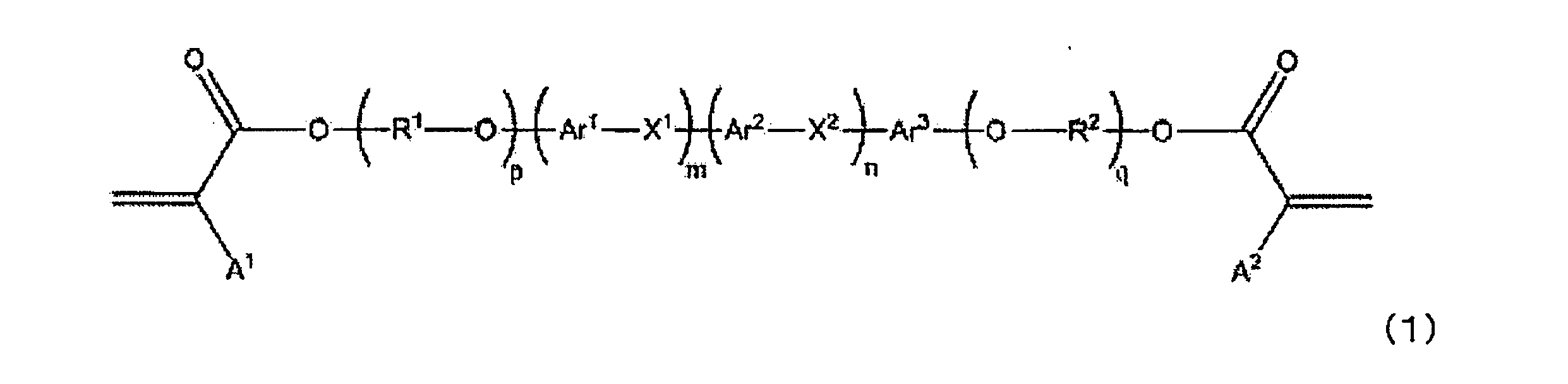
[式(1)中、A1及びA2はそれぞれ独立に、水素原子またはメチル基を表し、
Ar1、Ar2及びAr3は、それぞれ独立に、置換基を有してもよい2価の芳香族炭化水素環基または置換基を有してもよい2価の芳香族複素環基を表し、
X1及びX2はそれぞれ独立に、直接結合、炭素二重結合、炭素三重結合、エーテル結合、エステル結合、置換基を有していてもよい炭素数1~6の直鎖状アルキレン基、置換基を有していてもよい炭素数1~6の直鎖状オキシアルキレン基を表し、
R1及びR2は、それぞれ独立に、置換基を有していてもよい炭素数1~6の直鎖状アルキレン基、置換基を有していてもよい炭素数1~6の直鎖状オキシアルキレン基、又は炭素数2~6の直鎖状アルキルエステル基を表し、
m、n、p及びqは、それぞれ独立に、0または1を表す。
ただし、Ar1、Ar2及びAr3のうち、少なくともいずれか1つは、置換基を有してもよい2価の芳香族炭化水素縮合環基又は置換基を有してもよい2価の芳香族複素環基を表す。]
〔10〕前記一般式(1)で表される高分子前駆体が、下記一般式(2)で表されることを特徴とする前記〔9〕に記載の画像表示装置。
Ar1、Ar2及びAr3は、それぞれ独立に、置換基を有してもよい2価の芳香族炭化水素環基または置換基を有してもよい2価の芳香族複素環基を表し、
X1及びX2はそれぞれ独立に、直接結合、炭素二重結合、炭素三重結合、エーテル結合、エステル結合、置換基を有していてもよい炭素数1~6の直鎖状アルキレン基、置換基を有していてもよい炭素数1~6の直鎖状オキシアルキレン基を表し、
R1及びR2は、それぞれ独立に、置換基を有していてもよい炭素数1~6の直鎖状アルキレン基、置換基を有していてもよい炭素数1~6の直鎖状オキシアルキレン基、又は炭素数2~6の直鎖状アルキルエステル基を表し、
m、n、p及びqは、それぞれ独立に、0または1を表す。
ただし、Ar1、Ar2及びAr3のうち、少なくともいずれか1つは、置換基を有してもよい2価の芳香族炭化水素縮合環基又は置換基を有してもよい2価の芳香族複素環基を表す。]
〔10〕前記一般式(1)で表される高分子前駆体が、下記一般式(2)で表されることを特徴とする前記〔9〕に記載の画像表示装置。

[式(2)中、A1及びA2はそれぞれ独立に、水素原子またはメチル基を表し、
Ar4は、置換基を有してもよい2価の芳香族炭化水素縮合環基または置換基を有してもよい2価の芳香族複素縮合環基を表し、
R1及びR2は、それぞれ独立に、置換基を有していてもよい炭素数1~6の直鎖状アルキレン基、置換基を有していてもよい炭素数1~6の直鎖状オキシアルキレン基、又は炭素数2~6の直鎖状アルキルエステル基を表し、
p及びqは、それぞれ独立に、0または1を表す。]
〔11〕前記一般式(2)のAr4が置換基を有していてもよい2価のナフタレン環であることを特徴とする前記〔10〕に記載の画像表示装置。
〔12〕電圧無印加時に光透過状態で、電圧印加することで光散乱状態に切り替えできるスクリーンであって、
該スクリーンの光透過状態と光散乱状態が周期的に切り替わり、前記切り替わりの周波数が40Hz以上100Hz以下であり、かつ周期的切り替わりのデューティー比が0.01以上0.20以下のバースト電圧を印加した時の、スクリーンの光散乱状態部分のヘイズが、20%以下であり、
前記スクリーンが、少なくとも一方が透明な透明基板と、対向して配置される一対の電極付き基板を有し、前記一対の電極付き基板の間に、誘電率異方性が正であるカイラルネマチック液晶相と高分子樹脂相を含む複合体を含む液晶調光層を有することを特徴とするスクリーン。
Ar4は、置換基を有してもよい2価の芳香族炭化水素縮合環基または置換基を有してもよい2価の芳香族複素縮合環基を表し、
R1及びR2は、それぞれ独立に、置換基を有していてもよい炭素数1~6の直鎖状アルキレン基、置換基を有していてもよい炭素数1~6の直鎖状オキシアルキレン基、又は炭素数2~6の直鎖状アルキルエステル基を表し、
p及びqは、それぞれ独立に、0または1を表す。]
〔11〕前記一般式(2)のAr4が置換基を有していてもよい2価のナフタレン環であることを特徴とする前記〔10〕に記載の画像表示装置。
〔12〕電圧無印加時に光透過状態で、電圧印加することで光散乱状態に切り替えできるスクリーンであって、
該スクリーンの光透過状態と光散乱状態が周期的に切り替わり、前記切り替わりの周波数が40Hz以上100Hz以下であり、かつ周期的切り替わりのデューティー比が0.01以上0.20以下のバースト電圧を印加した時の、スクリーンの光散乱状態部分のヘイズが、20%以下であり、
前記スクリーンが、少なくとも一方が透明な透明基板と、対向して配置される一対の電極付き基板を有し、前記一対の電極付き基板の間に、誘電率異方性が正であるカイラルネマチック液晶相と高分子樹脂相を含む複合体を含む液晶調光層を有することを特徴とするスクリーン。
本発明の画像表示装置は、公告板、コンピューター端末、プロジェクション等に用いることができる。
以下に記載する構成要件の説明は、本発明の実施態様の一例(代表例)であり、これらの内容に特定されない。
本発明の画像表示装置は、スクリーンと、前記スクリーンに画像を投影するための画像投影機から構成され、少なくとも一つのスクリーンが画像投影機に対して配置されたものである。
本発明の画像表示装置は、スクリーンと、前記スクリーンに画像を投影するための画像投影機から構成され、少なくとも一つのスクリーンが画像投影機に対して配置されたものである。
本発明のスクリーンは、光透過状態と光散乱状態とで切り替えができ、該スクリーンが光散乱状態である時又は光透過状態から光散乱状態となる間に、前記画像投影機が前記スクリーンの一部または全体に対して画像を投影し、前記スクリーンが光透過状態の時に前記画像投影機による画像の投影を行わないように、スクリーンと画像投影機の同期を行なう。この同期切り替えを、人間の目では追随できない速度で繰り返すことによって、スクリーンに画像が投影された時に、画像が浮き出て見えるのである。なお、本明細書中で、特に断りが無い場合には、光とは可視光(波長380~800nm)を指す。
本発明に用いるスクリーンは、電圧無印加時に光透過状態で、電圧印加することで光散乱状態に切り替え可能なスクリーンである。本発明のスクリーンは、例えば窓やショーケースのような用途において、通常時(電圧無印加)に透明であり、電圧印加時に光散乱状態で画像を表示させることができるため、省エネルギーの観点からも有用である。
スクリーンは、該スクリーンに含まれる少なくとも一方が透明な透明基板と、対向して配置される一対の電極付き基板を有し、前記一対の電極付き基板の間に、誘電率異方性が正であるカイラルネマチック液晶相と高分子樹脂相を含む複合体を含む液晶調光層を有している。光透過状態と光散乱状態の切り替えは、液晶調光層を電気駆動することで実現できる。液晶調光層としては、光透過状態と光散乱状態を電気駆動により切り替えることのできる透過-散乱型の液晶相と高分子樹脂相の複合体を使用することができる。
スクリーンは、該スクリーンに含まれる少なくとも一方が透明な透明基板と、対向して配置される一対の電極付き基板を有し、前記一対の電極付き基板の間に、誘電率異方性が正であるカイラルネマチック液晶相と高分子樹脂相を含む複合体を含む液晶調光層を有している。光透過状態と光散乱状態の切り替えは、液晶調光層を電気駆動することで実現できる。液晶調光層としては、光透過状態と光散乱状態を電気駆動により切り替えることのできる透過-散乱型の液晶相と高分子樹脂相の複合体を使用することができる。
本発明に用いる液晶調光層は、電圧無印加時に光透過状態であり、閾値以上の実効値を持つ、直流電圧、交流電圧、パルス電圧またはそれらの組み合わせによって光散乱状態に切り替えられることを特徴とする。液晶調光層としては、印加電圧を取り除くと光透過状態に戻る、リバースモードの駆動をするものでもよいし、光透過状態と光散乱状態の切り替え時のみ電圧印加を行うメモリモードの駆動をするものを用いてもよい。
本発明のスクリーンは、光透過状態と光散乱状態のコントラストが高く、そのため、画像投影機の光源を特に強くしなくとも、鮮明な画像を表示させることができるのである。
本発明のスクリーンは、光透過状態と光散乱状態のコントラストが高く、そのため、画像投影機の光源を特に強くしなくとも、鮮明な画像を表示させることができるのである。
前記スクリーンは、光透過状態と光散乱状態が周期的に切り替わり、周波数が40Hz以上、100Hz以下であるように駆動させることを特徴とする。なお、本発明における光散乱状態とは、平行光線透過率が30%未満の状態を指し、本発明における光透過状態とは、平行光線透過率が80%以上の状態を指す。スクリーンを光透過状態と光散乱状態とで周期的に切り替えて駆動させている状態を、表示モードと表現することがある。
なお、光透過状態と光散乱状態を切り替える場合には、通常、中間的な過渡状態を経由するので、表示モードで駆動させている間に平行光線透過率が一時的に30%以上80%未満の状態をとってもよい。また、通常周期駆動とは毎周期まったく同じく駆動をすることを指すが、本発明の趣旨を外れない範囲でなら一部異なった駆動が入っていてもよい。
本発明に用いるスクリーンの光透過状態と光散乱状態の周期的切り替わりは、周波数が40Hz以上、好ましくは45Hz以上であり、100Hz以下、好ましくは70Hz以下、さらに好ましくは60Hz以下である。周波数が40Hzより小さい場合は、表示モードでスクリーン上にちらつきが生じる。
周波数が大きいほどちらつきは小さくなる傾向があるが、スクリーンの応答速度がこの周波数に追随できない場合には、光散乱状態の平行光線透過率が十分には低下しなくなり、映像の視認性が低下することがある。周波数が特定の範囲であることにより、ちらつきがなく、かつ視認性も十分良好な表示を得ることができる。
本発明に用いるスクリーンの光透過状態と光散乱状態の周期的切り替わりは、周波数が40Hz以上、好ましくは45Hz以上であり、100Hz以下、好ましくは70Hz以下、さらに好ましくは60Hz以下である。周波数が40Hzより小さい場合は、表示モードでスクリーン上にちらつきが生じる。
周波数が大きいほどちらつきは小さくなる傾向があるが、スクリーンの応答速度がこの周波数に追随できない場合には、光散乱状態の平行光線透過率が十分には低下しなくなり、映像の視認性が低下することがある。周波数が特定の範囲であることにより、ちらつきがなく、かつ視認性も十分良好な表示を得ることができる。
また、本発明に用いるスクリーンの周期的切り替わりのデューティー比は、0.01以上、0.20以下である。前記スクリーンのデューティー比とは、光透過状態と光散乱状態の周期的切り替わりにおける、光散乱状態である時間の割合である。
本発明のスクリーンの周期的切り替わりのデューティー比は0.01以上、好ましくは0.05以上であり、一方上限は、0.20以下、好ましくは0.15以下である。デューティー比は小さいほど表示モードでのスクリーンのヘイズが小さくなり、背景の透過性が向上する。デューティー比が0.20以下であることで、表示モードで画像を表示させた場合に室内等の暗い場所でも背景が良く見える。一方でデューティー比は大きいほど、表示映像が鮮明になる傾向がある。デューティー比が特定の範囲であることで、映像の視認性と背景の透過性を両立することができる。
本発明のスクリーンの周期的切り替わりのデューティー比は0.01以上、好ましくは0.05以上であり、一方上限は、0.20以下、好ましくは0.15以下である。デューティー比は小さいほど表示モードでのスクリーンのヘイズが小さくなり、背景の透過性が向上する。デューティー比が0.20以下であることで、表示モードで画像を表示させた場合に室内等の暗い場所でも背景が良く見える。一方でデューティー比は大きいほど、表示映像が鮮明になる傾向がある。デューティー比が特定の範囲であることで、映像の視認性と背景の透過性を両立することができる。
本発明における周期的切り替わりにおいて、スクリーンの平行光線透過率が30%以上の時間をτOFF、平行光線透過率が30%未満の時間をτONとするとき、τON/(τON+τOFF)が、好ましくは0.01以上であり、さらに好ましくは0.05以上である。一方、好ましくは0.20以下であり、さらに好ましくは0.15以下である。τON/(τON+τOFF)が特定の範囲であることで、映像の視認性と背景の透過性を両立することができる。
また、平行光線透過率はT=I/I0によって測定できる。ここでIは試料を透過させた光の放射発散度であり、I0は入射光の放射発散度である。瞬間的な平行光線透過率は、市販の高速対応分光器や高速対応輝度計等を用いることで測定できる。
本発明の表示モードは、前記液晶調光層に周波数が40Hz以上、100Hz以下であり、かつ液晶調光層の閾値を超える実効値を持つパルス電圧のデューティー比が0.01以上0.20以下であるバースト電圧を印加することで実現できる(以下、パルス電圧又はバースト電圧と表現する場合がある)。
また、平行光線透過率はT=I/I0によって測定できる。ここでIは試料を透過させた光の放射発散度であり、I0は入射光の放射発散度である。瞬間的な平行光線透過率は、市販の高速対応分光器や高速対応輝度計等を用いることで測定できる。
本発明の表示モードは、前記液晶調光層に周波数が40Hz以上、100Hz以下であり、かつ液晶調光層の閾値を超える実効値を持つパルス電圧のデューティー比が0.01以上0.20以下であるバースト電圧を印加することで実現できる(以下、パルス電圧又はバースト電圧と表現する場合がある)。
通常は、スクリーンの液晶調光層に電圧が印加された場合、光散乱状態に切り替わる際の平行光線透過率が減少しきるためには有限の時間を要し、一方、光透過状態に切り替わる際の平行光線透過率が増加しきるのにもやはり有限の時間を要する。平行光線透過率が時間とともに変動するこれら過渡状態があることで、本来光透過状態であってほしいタイミングで、平行光線透過率が低かったり、本来光散乱状態であってほしいタイミングで平行光線透過率が高いという不都合が生じ、その結果、表示モードの透過性が減少したり、表示画像の視認性が低下することが起きる。
本明細書中に記載の応答時間を図1を参照して説明する。スクリーンが電圧無印加時の平行光線透過率をTmax、電圧印加時の平行光線透過率の最小値をTminとし、パルス電圧印加開始時刻をt1、印加終了時刻をt2としたとき、立ち上がりの応答時間をτ1、立ち下がりの応答時間をτ2とすると、τ1はt1から初めて平行光線透過率がT10に到達するまでの時間であり、τ2はt2から初めて平行光線透過率がT90に到達するまでの時間であると定義する。ただし、T10、T90はそれぞれ、以下で表される。
T10=0.1×(Tmax-Tmin)
T90=0.9×(Tmax-Tmin)
T10=0.1×(Tmax-Tmin)
T90=0.9×(Tmax-Tmin)
本発明のスクリーンに周波数が40Hz以上100Hz以下であり、かつデューティー比が0.01以上0.20以下のバースト電圧を印加し、スクリーンが光透過状態から光散乱状態へ変化し、さらに光透過状態に戻る過程において、スクリーンの立ち上がりの応答時間τ1と立ち下がりの応答時間τ2が、いずれも3.0ms以下であることが好ましい。さらに好ましくはいずれも2.0ms以下である。
τ1またはτ2が印加電圧のパルス幅に比べて同程度以上に長くないことで、映像の視認性と背景の透過性の両立ができる傾向にある。
本発明におけるスクリーンの周期駆動と画像投影機との同期では、画像投影機が画像を投影している期間において、好ましくはスクリーンの平行光線透過率が30%未満であり、さらに好ましくは20%未満である。それ以外の期間はスクリーンの平行光線透過率が高いほどよく、好ましくは80%以上である。これに対し、スクリーンの平行光線透過率が30%以上、80%未満である過渡状態は、映像を投影しても十分な視認性が得られず、かといって透明性も低い、過渡状態である。本発明で用いるスクリーンでは、この過渡状態を短くすることができ、したがって映像の視認性と背景の透過性を両立することができる。また、τ1とτ2の値は同一又は近似値である方が、同期制御が容易になり好ましい。
本発明におけるスクリーンの周期駆動と画像投影機との同期では、画像投影機が画像を投影している期間において、好ましくはスクリーンの平行光線透過率が30%未満であり、さらに好ましくは20%未満である。それ以外の期間はスクリーンの平行光線透過率が高いほどよく、好ましくは80%以上である。これに対し、スクリーンの平行光線透過率が30%以上、80%未満である過渡状態は、映像を投影しても十分な視認性が得られず、かといって透明性も低い、過渡状態である。本発明で用いるスクリーンでは、この過渡状態を短くすることができ、したがって映像の視認性と背景の透過性を両立することができる。また、τ1とτ2の値は同一又は近似値である方が、同期制御が容易になり好ましい。
本発明のスクリーンの光散乱状態部分のヘイズは、JIS K7136(2000年)の測定方法で定義される。なお、本明細書中でヘイズは時間平均として測定されたものをいう。
また、本発明の画像表示装置における表示画像の放射輝度は、JIS Z8724(1997年)で測定される分光放射輝度を可視光波長領域で積分することで算出される。
また、本発明の画像表示装置における表示画像の放射輝度は、JIS Z8724(1997年)で測定される分光放射輝度を可視光波長領域で積分することで算出される。
周期的切り替わりのデューティー比を調整することで、背景と映像のどちらを強調するか選択することが可能である。すなわち、周期的切り替わりのデューティー比を小さくすることで、表示モードにおけるスクリーンのヘイズを小さくすることができるが、表示映像の放射輝度も小さくなる。逆に周期的切り替わりのデューティー比を大きくすることで、表示モードにおけるスクリーンのヘイズが大きくなるが、表示映像の放射輝度が大きくなる。
周波数が40Hz以上100Hz以下であり、かつデューティー比が0.01以上0.20以下のバースト電圧を印加したときの表示モードにおけるヘイズは、20%以下であることが好ましく、15%以下であることが更に好ましい。また、1%以上が好ましく、5%以上が更に好ましい。ヘイズが大きすぎないことで、背景の透過性が良好になり傾向にあり、小さすぎないことで、表示映像の輝度が視認可能な程度に確保できる傾向にある。
周波数が40Hz以上100Hz以下であり、かつデューティー比が0.01以上0.20以下のバースト電圧を印加したときの表示モードにおけるヘイズは、20%以下であることが好ましく、15%以下であることが更に好ましい。また、1%以上が好ましく、5%以上が更に好ましい。ヘイズが大きすぎないことで、背景の透過性が良好になり傾向にあり、小さすぎないことで、表示映像の輝度が視認可能な程度に確保できる傾向にある。
本発明におけるスクリーンと画像投影機の位置関係は、スクリーンを挟んで観察者と画像投影機が対向するリアプロジェクション方式でもよく、スクリーンに対して観察者と画像投影機が同じ側にいるフロントプロジェクション方式でもよい。光散乱状態の液晶調光層において、後方散乱が強い場合には前者を、前方散乱が強い場合には後者を用いればよい。スクリーンに対して画像投影機の光射出口が垂直になるように設置してもよいし、角度をつけて設置してもよい。観察者の視界の妨げにならないように画像投影機をスクリーンに対して見えなくなる程度に角度をつけて設置することもできる。この場合、投影された画像の形状をスクリーンの表示部分に合わせて補正することが好ましい。
本発明の画像表示装置における黒表示は、画像投影機から光がスクリーンへ投影されていない(R,G,B)=(0,0,0)の状態である。また白表示は、画像投影機から投影される光の放射輝度が等しく最大である(R,G,B)=(255,255,255)の状態である。表示画像のコントラストは、(白表示の放射輝度)/(黒表示の放射輝度)で計算される。
本発明のスクリーンは、画像の特定範囲の入射方向において、輝度の比が特定の値であることが好ましい。具体的には、画像投影装置のスクリーンが光散乱状態である時に、画像投影機が前記スクリーンの一部または全体に対して画像を投影し、前記スクリーンが光透過状態の時に前記画像投影機による画像の投影を行わないように同期せしめる。この時に、前記スクリーンの光透過状態と光散乱状態が周期的に切り替わるように駆動させる。このように駆動させた場合において、スクリーンに対して、画像投影機から投影された画像の入射方向が30°以内において、黒表示に対する白表示の放射輝度の比が30以上であることが好ましい。さらに、60以上であることが好ましい。
このような表示特性を満たすことで、斜め方向からスクリーンを見た時でも画像の視認性が良好となる。また、スクリーンに対し斜め方向からを投影した場合でも、視認性が良好となる。
本発明の画像表示装置において、このような視認性が良好となるのは、以下の理由からである。本発明で用いるスクリーンの液晶調光層は、カイラルネマチック液晶のフォーカルコニック相と網目状のポリマーとの複合構造により光を散乱させる。ランダムな液晶ポリドメイン構造であるフォーカルコニック相とランダムな網目状ポリマー構造により、入射光が広範囲に散乱され、広い視野角が与えられることにより、本発明のスクリーンは上述したようなめ方向からスクリーンを見た時でも画像の視認性が良好となるのである。
このような表示特性を満たすことで、斜め方向からスクリーンを見た時でも画像の視認性が良好となる。また、スクリーンに対し斜め方向からを投影した場合でも、視認性が良好となる。
本発明の画像表示装置において、このような視認性が良好となるのは、以下の理由からである。本発明で用いるスクリーンの液晶調光層は、カイラルネマチック液晶のフォーカルコニック相と網目状のポリマーとの複合構造により光を散乱させる。ランダムな液晶ポリドメイン構造であるフォーカルコニック相とランダムな網目状ポリマー構造により、入射光が広範囲に散乱され、広い視野角が与えられることにより、本発明のスクリーンは上述したようなめ方向からスクリーンを見た時でも画像の視認性が良好となるのである。
本発明のスクリーンは、電圧無印加時に光透過状態であり、この時のヘイズが10%以下であることが好ましい。さらに8%以下が好ましく、5%以下が特に好ましい。また、電圧印加時に光散乱状態となり、スクリーンに直流電圧または交流電圧の連続波を印加することで、ヘイズが85%以上に切り替わることが好ましく、90%以上になることが好ましい。また上限は100%であり、高いほど好ましい。これらの範囲であることで表示映像の視認性が良好になる傾向にある。
本発明のスクリーンの動作温度上限はカイラルネマチック液晶相の液晶-等方相転移温度(Tni)であるが、低温では応答時間が長くなる傾向がある。従って、動作温度範囲としては、好ましくは-10℃以上、更に好ましくは0℃以上である。また、好ましくは60℃以下であり、更に好ましくは40℃以下である。本発明のスクリーンは、少なくとも一方が透明な透明基板と、対向して配置される一対の電極付き基板を有し、前記一対の電極付き基板の間に、誘電率異方性が正であるカイラルネマチック液晶相と高分子樹脂相を含む複合体を含む液晶調光層を有する。
<液晶調光層>
本発明のスクリーンに用いる液晶調光層は、誘電率異方性が正であるカイラルネマチック液晶相と高分子樹脂相を含む複合体を含む。この方式は、PSCTとして知られている。
以下、リバースモードPSCTの駆動モードについて説明する。リバースモードPSCTでは、電圧無印加時には液晶らせん軸がほぼ全て基板に対して垂直方向を向くプレナー相となり、光透過状態を取る。液晶調光層の電極基板間に電圧を印加することで、液晶らせん軸がランダムな方向を向くフォーカルコニック相へと相転移し、光散乱状態となる。この2つの相をスイッチングすることで、スクリーンの平行光線透過率を制御することができる。
ところで、液晶調光層の電極基板間にさらに高電圧を印加すると、液晶分子長軸が基板と垂直な方向を向くホメオトロピック相へと相転移し、光透過状態となる。
本発明のスクリーンに用いる液晶調光層は、誘電率異方性が正であるカイラルネマチック液晶相と高分子樹脂相を含む複合体を含む。この方式は、PSCTとして知られている。
以下、リバースモードPSCTの駆動モードについて説明する。リバースモードPSCTでは、電圧無印加時には液晶らせん軸がほぼ全て基板に対して垂直方向を向くプレナー相となり、光透過状態を取る。液晶調光層の電極基板間に電圧を印加することで、液晶らせん軸がランダムな方向を向くフォーカルコニック相へと相転移し、光散乱状態となる。この2つの相をスイッチングすることで、スクリーンの平行光線透過率を制御することができる。
ところで、液晶調光層の電極基板間にさらに高電圧を印加すると、液晶分子長軸が基板と垂直な方向を向くホメオトロピック相へと相転移し、光透過状態となる。
<カイラルネマチック液晶>
本発明のスクリーンに用いるカイラルネマチック液晶は、誘電率異方性が正である。本発明のカイラルネマチック液晶の該誘電率異方性が正であることで、Tminの低下およびτ1、τ2の短縮を両立できる。
カイラルネマチック液晶の誘電率異方性値(Δε)は正であれば特に限定されないが、5以上であることが好ましく、8以上であることが、スクリーンの駆動電圧低減のために好ましい。また、重合開始剤を使用する場合、カイラルネマチック液晶を構成する個々の分子が開始剤の吸収波長に重なる波長の吸収を持たないことが、重合性モノマーの硬化時間を短くする点で好ましい。
本発明のスクリーンに用いるカイラルネマチック液晶は、誘電率異方性が正である。本発明のカイラルネマチック液晶の該誘電率異方性が正であることで、Tminの低下およびτ1、τ2の短縮を両立できる。
カイラルネマチック液晶の誘電率異方性値(Δε)は正であれば特に限定されないが、5以上であることが好ましく、8以上であることが、スクリーンの駆動電圧低減のために好ましい。また、重合開始剤を使用する場合、カイラルネマチック液晶を構成する個々の分子が開始剤の吸収波長に重なる波長の吸収を持たないことが、重合性モノマーの硬化時間を短くする点で好ましい。
カイラルネマチック液晶としては、液晶自身がコレステリック相を示す液晶性化合物の集合でもよく、ネマチック液晶にカイラル剤を添加することでカイラルネマチック液晶としたものでもよい。液晶組成物設計の観点では、目的に応じてネマチック液晶にカイラル剤を添加し、カイラルピッチ長(p)および液晶-等方相転移温度(Tni)を制御することが好ましい。
立ち上がりの応答時間τ1を短くするためには、液晶調光層の電極基板間へなるべく高い電圧を印加した方が有利である。ところが印加電圧が高すぎると、ホメオトロピック相へと相転移してしまい、十分な光散乱が得られなくなるというジレンマがある。この課題を解決するためには、電極付き基板間の距離をdとし、カイラルネマチック液晶のカイラルピッチ長をpとするとき、d/pの値が1以上であることが好ましい。d/pはより好ましくは、2以上、更に好ましくは4以上である。また、d/pは20以下であることが好ましく、12以下であることが特に好ましい。
d/pが大きいほど、駆動時の散乱が大きくなり、遮光特性が向上する。またd/pが大きいほど、フォーカルコニック相からホメオトロピック相への閾値電圧が高くなり、高電圧を印加しても光透過状態へ相転移せず、光散乱状態を維持することができる。そのため立ち上がりの応答時間τ1を短くすることができる。一方でスクリーンの駆動電圧(プレナー相からフォーカルコニック相への閾値電圧)も同時に増加するため、遮光特性と省エネや安全性の両立の観点から、上記の範囲内に収めることが好適である。
d/pが大きいほど、駆動時の散乱が大きくなり、遮光特性が向上する。またd/pが大きいほど、フォーカルコニック相からホメオトロピック相への閾値電圧が高くなり、高電圧を印加しても光透過状態へ相転移せず、光散乱状態を維持することができる。そのため立ち上がりの応答時間τ1を短くすることができる。一方でスクリーンの駆動電圧(プレナー相からフォーカルコニック相への閾値電圧)も同時に増加するため、遮光特性と省エネや安全性の両立の観点から、上記の範囲内に収めることが好適である。
カイラルネマチック液晶のカイラルピッチ長pは、0.3μm以上が好ましく、0.8μm以上が更に好ましい。一方、カイラルピッチ長pは、3μm以下が好ましく、2μm以下が更に好ましい。
カイラルピッチ長pが小さ過ぎないことで、スクリーンの駆動電圧が低く抑えられる傾向があり、大き過ぎないことで、コントラスが高くなる傾向となる。
一般にpはカイラル剤の濃度に反比例するので、必要なカイラルピッチ長pの値から逆算してカイラル剤の濃度を決定すればよい。なお、p×n(nはカイラルネマチック液晶の屈折率)が可視光波長(380nm~800nm)の範囲内にある場合、最終的に得られるスクリーンは電圧無印加時に有色となり、可視光範囲外にある場合は電圧無印加時に無色透明になるので、カイラルピッチ長pは、目的に応じてpを選択すればよい。
カイラルピッチ長pが小さ過ぎないことで、スクリーンの駆動電圧が低く抑えられる傾向があり、大き過ぎないことで、コントラスが高くなる傾向となる。
一般にpはカイラル剤の濃度に反比例するので、必要なカイラルピッチ長pの値から逆算してカイラル剤の濃度を決定すればよい。なお、p×n(nはカイラルネマチック液晶の屈折率)が可視光波長(380nm~800nm)の範囲内にある場合、最終的に得られるスクリーンは電圧無印加時に有色となり、可視光範囲外にある場合は電圧無印加時に無色透明になるので、カイラルピッチ長pは、目的に応じてpを選択すればよい。
本発明のスクリーンの電極付き基板間の距離dは、使用するカイラルネマチック液晶のカイラルピッチ長p以上である必要があり、通常3μm以上が好ましく、5μm以上が更に好ましい。また、距離dは100μm以下が好ましく、20μm以下が更に好ましい。
電圧を印加していない状態でのスクリーンの光透過率は、距離dの増加に対して減少し、また、表示ディスプレイの応答時間も長くなる場合がある。一方で、dが小さすぎることで、駆動時の遮光特性が低減し、また大面積のスクリーンの場合、スクリーンが短絡してしまう場合がある。上記範囲であることで、これらの要求をバランスよく満足することができる。
電圧を印加していない状態でのスクリーンの光透過率は、距離dの増加に対して減少し、また、表示ディスプレイの応答時間も長くなる場合がある。一方で、dが小さすぎることで、駆動時の遮光特性が低減し、また大面積のスクリーンの場合、スクリーンが短絡してしまう場合がある。上記範囲であることで、これらの要求をバランスよく満足することができる。
カイラルネマチック液晶のTniは、スクリーンの動作可能な温度上限がカイラルネマチック液晶のTniにより決定されることから50℃以上が好ましく、70℃以上が更に好ましい。一方、Tniが高くなると粘度が高くなる傾向があるので、200℃以下が好ましく、150℃以下が更に好ましい。
ネマチック液晶としては、公知のいずれでもよく、構成分子の分子骨格、置換基、分子量に制限は特になく、合成品でも市販品でもよい。ネマチック液晶の誘電率異方性は正で大きいことが、スクリーンのカイラルネマチック液晶相及び液晶組成物のカイラルネマチック液晶の誘電率異方性を正とするために好ましい。また、重合開始剤を用いる場合、構成分子が構成する個々の分子が開始剤の吸収波長に重なる波長の吸収を持たないことが、重合性モノマーの硬化時間を短くする点で好ましい。
ネマチック液晶としては、公知のいずれでもよく、構成分子の分子骨格、置換基、分子量に制限は特になく、合成品でも市販品でもよい。ネマチック液晶の誘電率異方性は正で大きいことが、スクリーンのカイラルネマチック液晶相及び液晶組成物のカイラルネマチック液晶の誘電率異方性を正とするために好ましい。また、重合開始剤を用いる場合、構成分子が構成する個々の分子が開始剤の吸収波長に重なる波長の吸収を持たないことが、重合性モノマーの硬化時間を短くする点で好ましい。
公知の液晶性物質を用いる場合、具体的には日本学術振興会第142委員会編;「液晶デバイスハンドブック」日本工業新聞社(1989年)、第152頁~第192頁および液晶便覧編集委員会編;「液晶便覧」丸善株式会社(2000年)、第260頁~第330頁に記載されているようなビフェニル系、フェニルシクロヘキサン系、シクロヘキシルシクロヘキサン系などの各種低分子系の化合物または混合物を使用することができる。また、液晶便覧編集委員会編;「液晶便覧」丸善株式会社(2000年)、第365頁~第415頁に記載されているような高分子系化合物または混合物を使用することもできる。ネマチック液晶を構成する化合物としては例えば、以下の化合物等が挙げられる。

コレステリック液晶およびネマチック液晶としては粘度が低く、誘電率異方性の高いものが、スクリーンの高速応答性や製造性の点で好ましい。
カイラル剤としては、ホスト液晶へ相溶するカイラル化合物であればいずれでもよく、合成品でも市販品でよく、自身が液晶性を示すものでもよいし、重合性の官能基を有していてもよい。また、右旋性でも左旋性でもよく、右旋性のカイラル剤と左旋性のカイラル剤を併用してもよい。また、カイラル剤としては、それ自身の誘電異方性が正に大きく、粘度の低いものがスクリーンの駆動電圧低減および応答速度の観点から好ましく、カイラル剤が液晶をねじる力の指標とされるHelical Twisting Powerが大きいほうが好ましい。重合開始剤を用いる場合には、開始剤の吸収波長に重なる波長の吸収を持たないことが好ましい。
カイラル剤としては、例えばCB15(商品名、メルク社製)、C15(商品名、メルク社製)、S-811(商品名、メルク社製)、R-811(商品名、メルク社製)、S-1011(商品名、メルク社製)、R-1011(商品名メルク社製)などが挙げられる。
カイラル剤としては、ホスト液晶へ相溶するカイラル化合物であればいずれでもよく、合成品でも市販品でよく、自身が液晶性を示すものでもよいし、重合性の官能基を有していてもよい。また、右旋性でも左旋性でもよく、右旋性のカイラル剤と左旋性のカイラル剤を併用してもよい。また、カイラル剤としては、それ自身の誘電異方性が正に大きく、粘度の低いものがスクリーンの駆動電圧低減および応答速度の観点から好ましく、カイラル剤が液晶をねじる力の指標とされるHelical Twisting Powerが大きいほうが好ましい。重合開始剤を用いる場合には、開始剤の吸収波長に重なる波長の吸収を持たないことが好ましい。
カイラル剤としては、例えばCB15(商品名、メルク社製)、C15(商品名、メルク社製)、S-811(商品名、メルク社製)、R-811(商品名、メルク社製)、S-1011(商品名、メルク社製)、R-1011(商品名メルク社製)などが挙げられる。
<高分子樹脂相>
本発明の高分子樹脂相は、特定の高分子前駆体を硬化してなることが好ましい。
本発明の高分子樹脂相は、前記カイラルネマチック液晶相に対し、10質量%以下であることが好ましく、7質量%以下であることが更に好ましい。また、0.1質量%以上であることが好ましく、1質量%以上であることが好ましい。高分子樹脂相の割合が少な過ぎないことで、高分子樹脂相が機械的に強靭となり、繰り返し耐久性に優れる傾向となる。また、液晶分子が十分な界面相互作用を受けられるため、スクリーンのコントラストおよび応答速度が高くなる場合がある。一方で、高分子樹脂相の割合が多過ぎないことで、駆動電圧の上昇が抑えられ、スクリーンの透明性が高くなる傾向にある。
本発明の高分子樹脂相は、特定の高分子前駆体を硬化してなることが好ましい。
本発明の高分子樹脂相は、前記カイラルネマチック液晶相に対し、10質量%以下であることが好ましく、7質量%以下であることが更に好ましい。また、0.1質量%以上であることが好ましく、1質量%以上であることが好ましい。高分子樹脂相の割合が少な過ぎないことで、高分子樹脂相が機械的に強靭となり、繰り返し耐久性に優れる傾向となる。また、液晶分子が十分な界面相互作用を受けられるため、スクリーンのコントラストおよび応答速度が高くなる場合がある。一方で、高分子樹脂相の割合が多過ぎないことで、駆動電圧の上昇が抑えられ、スクリーンの透明性が高くなる傾向にある。
本発明の高分子樹脂相に用いられる高分子樹脂は、本発明の効果を損なわなければ特に限定されないが、下記一般式(1)で表される高分子前駆体を含む混合物を硬化させたものを用いることが、スクリーンの電圧印加時の平行光線透過率の最小値Tminの低減、およびτ1、τ2の短縮を両立できる傾向があるため好ましい。
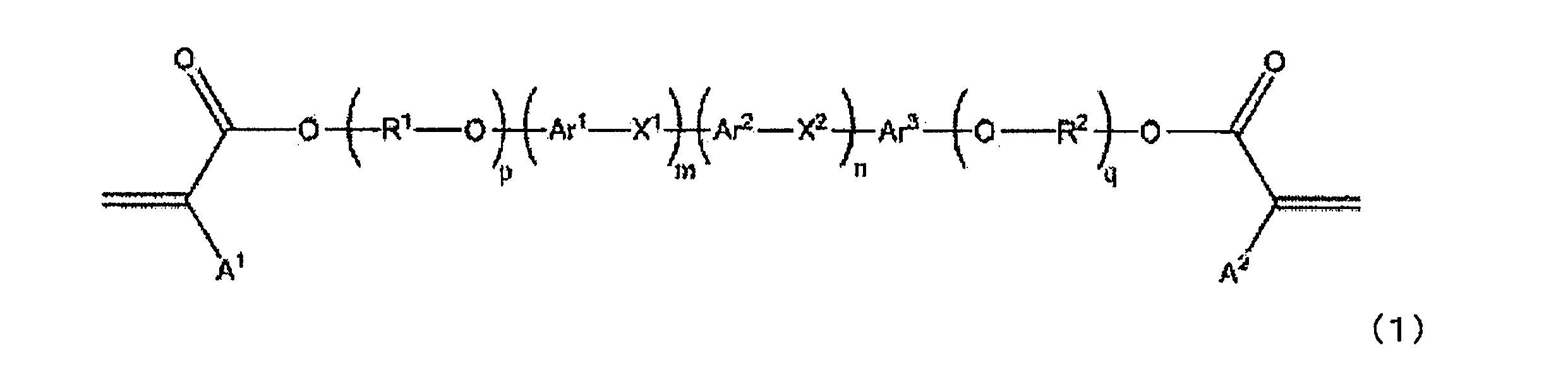
[式(1)中、A1及びA2はそれぞれ独立に、水素原子またはメチル基を表し、
Ar1、Ar2及びAr3は、それぞれ独立に、置換基を有してもよい2価の芳香族炭化水素環基または置換基を有してもよい2価の芳香族複素環基を表し、
X1及びX2はそれぞれ独立に、直接結合、炭素二重結合、炭素三重結合、エーテル結合、エステル結合、置換基を有していてもよい炭素数1~6の直鎖状アルキレン基、置換基を有していてもよい炭素数1~6の直鎖状オキシアルキレン基を表し、
R1及びR2は、それぞれ独立に、置換基を有していてもよい炭素数1~6の直鎖状アルキレン基、置換基を有していてもよい炭素数1~6の直鎖状オキシアルキレン基、又は炭素数2~6の直鎖状アルキルエステル基を表し、
m、n、p及びqは、それぞれ独立に、0または1を表す。
ただし、Ar1、Ar2及びAr3のうち、少なくともいずれか1つは、置換基を有してもよい2価の芳香族縮合環基又は置換基を有してもよい2価の芳香族複素環基を表す。]
Ar1、Ar2及びAr3は、それぞれ独立に、置換基を有してもよい2価の芳香族炭化水素環基または置換基を有してもよい2価の芳香族複素環基を表し、
X1及びX2はそれぞれ独立に、直接結合、炭素二重結合、炭素三重結合、エーテル結合、エステル結合、置換基を有していてもよい炭素数1~6の直鎖状アルキレン基、置換基を有していてもよい炭素数1~6の直鎖状オキシアルキレン基を表し、
R1及びR2は、それぞれ独立に、置換基を有していてもよい炭素数1~6の直鎖状アルキレン基、置換基を有していてもよい炭素数1~6の直鎖状オキシアルキレン基、又は炭素数2~6の直鎖状アルキルエステル基を表し、
m、n、p及びqは、それぞれ独立に、0または1を表す。
ただし、Ar1、Ar2及びAr3のうち、少なくともいずれか1つは、置換基を有してもよい2価の芳香族縮合環基又は置換基を有してもよい2価の芳香族複素環基を表す。]
Ar1、Ar2及びAr3の置換基を有してもよい2価の芳香族炭化水素環基としては、本発明の効果を損なわないものであれば特に限定されないが、2価の芳香族炭化水素環基としては、単環、あるいはこれが2~4個縮合してなる縮合環から、水素原子を2個除いて得られる2価の基であり、具体例としては、ベンゼン環、ナフタレン環、アントラセン環、フェナントレン環、ペリレン環、テトラセン環、ピレン環、ベンズピレン環、クリセン環、トリフェニレン環、アセナフテン環、フルオランテン環、フルオレン環などの基が挙げられる。この中でも、炭素数が6以上であることが好ましく、一方、30以下、さら26以下、特に18以下であることが、重合時の硬化性の点から好ましい。具体的には、以下の構造等が挙げられる。

Ar1、Ar2及びAr3の置換基を有してもよい2価の芳香族炭化水素環基としては、上記の中でも特に以下の構造であることが、高分子前駆体の硬化性が高く好ましい。

Ar1、Ar2及びAr3の2価の芳香族炭化水素環基が有していてもよい置換基としては、フッ素原子、塩素原子、ヒドロキシル基、シアノ基、メチル基、エチル基、n-プロピル基、イソプロピル基、メトキシ基、エトキシ基、n-プロポキシ基、イソプロポキシ基、n-ブチル基、イソブチル基、t-ブチル基等が挙げられ、高分子前駆体の硬化性の点から、好ましくはフッ素原子、ヒドロキシル基、シアノ基、メチル基、メトキシ基である。
Ar1、Ar2及びAr3の置換基を有してもよい2価の芳香族複素環基としては、本発明の効果を損なわないものであれば特に限定はされないが、単環、あるいはこれが2~4個縮合してなる縮合環から、水素原子を2個除いて得られる2価の基であり、具体例としては、フラン環、ベンゾフラン環、チオフェン環、ベンゾチオフェン環、ピロール環、ピラゾール環、イミダゾール環、オキサジアゾール環、インドール環、カルバゾール環、ピロロイミダゾール環、ピロロピラゾール環、ピロロピロール環、チエノピロール環、チエノチオフェン環、フロピロール環、フロフラン環、チエノフラン環、ベンゾイソオキサゾール環、ベンゾイソチアゾール環、ベンゾイミダゾール環、ピリジン環、ピラジン環、ピリダジン環、ピリミジン環、トリアジン環、キノリン環、イソキノリン環、シノリン環、キノキサリン環、フェナントリジン環、ベンゾイミダゾール環、ペリミジン環、キナゾリン環、キナゾリノン環、アズレン環などの基が挙げられる。この中でも、炭素数が6以上であることが好ましく、一方、30以下、さら26以下、特に18以下であることが、重合時の硬化性の点から好ましい。具体的には、以下の構造等が挙げられる。

Ar1、Ar2及びAr3の置換基を有してもよい2価の芳香族複素環基としては、上記の中でも特に以下の構造であることが、高分子前駆体の硬化性が高く好ましい。

Ar1、Ar2及びAr3の2価の芳香族複素環基が有していてもよい置換基としては、フッ素原子、塩素原子、ヒドロキシル基、シアノ基、メチル基、エチル基、n-プロピル基、イソプロピル基、メトキシ基、エトキシ基、n-プロポキシ基、イソプロポキシ基、n-ブチル基、イソブチル基、t-ブチル基等が挙げられ、高分子前駆体の硬化性の点から、好ましくはフッ素原子、ヒドロキシル基、シアノ基、メチル基、メトキシ基である。
X1及びX2はそれぞれ独立に、直接結合、炭素二重結合、炭素三重結合、エーテル結合、エステル結合、置換基を有していてもよい炭素数1~6の直鎖状アルキレン基、置換基を有していてもよい炭素数1~6の直鎖状オキシアルキレン基を表し、好ましくは直接結合、エーテル結合、エステル結合、メチレン基である。有していてもよい置換基としては、フッ素原子、塩素原子、ヒドロキシル基、シアノ基、メチル基、エチル基、n-プロピル基、イソプロピル基、メトキシ基、エトキシ基、n-プロポキシ基、イソプロポキシ基、n-ブチル基、イソブチル基、t-ブチル基等が挙げられ、好ましくはフッ素原子、ヒドロキシル基、シアノ基、メチル基、メトキシ基である。
R1及びR2は、それぞれ独立に、置換基を有していてもよい炭素数1~6の直鎖状アルキレン基、置換基を有していてもよい炭素数1~6の直鎖状オキシアルキレン基、又は炭素数2~6の直鎖状アルキルエステル基を表す。炭素数2~6の直鎖状アルキルエステル基とは、例えば以下の構造を表す。

R1及びR2が有していてもよい置換基としては、フッ素原子、塩素原子、ヒドロキシル基、シアノ基、メチル基、エチル基、n-プロピル基、イソプロピル基、メトキシ基、エトキシ基、n-プロポキシ基、イソプロポキシ基、n-ブチル基、イソブチル基、t-ブチル基等が挙げられ、好ましくはフッ素原子、ヒドロキシル基、シアノ基、メチル基、メトキシ基である。
Ar1、Ar2及びAr3のうち、少なくともいずれか1つは、置換基を有してもよい2価の芳香族縮合環基又は置換基を有してもよい2価の芳香族複素環基である。置換基を有してもよい2価の芳香族縮合環基又は置換基を有してもよい2価の芳香族複素環基を分子内に持つことで、硬化後の高分子樹脂相の剛性が高くなり、τ1、τ2を短縮させる傾向があり、好ましい。
前記一般式(1)で表される高分子前駆体が、下記一般式(2)で表される高分子前駆体であることが更に好ましい。

[式(2)中、A1及びA2はそれぞれ独立に、水素原子またはメチル基を表し、
Ar4は、置換基を有してもよい2価の芳香族炭化水素縮合環基または置換基を有してもよい2価の複素縮合環基を表し、
R1及びR2は、それぞれ独立に、置換基を有していてもよい炭素数2~6のアルキレン基を表し、
p及びqは、それぞれ独立に、0または1を表す。]
Ar4の置換基を有してもよい2価の芳香族炭化水素環基及び置換基を有してもよい2価の複素環基としては、具体的には、Ar1で挙げたものと同義であり、有していてもよい置換基も同義である。この中でも、以下で表される構造が、高分子前駆体の硬化性が高くなるため、好ましい。
Ar4は、置換基を有してもよい2価の芳香族炭化水素縮合環基または置換基を有してもよい2価の複素縮合環基を表し、
R1及びR2は、それぞれ独立に、置換基を有していてもよい炭素数2~6のアルキレン基を表し、
p及びqは、それぞれ独立に、0または1を表す。]
Ar4の置換基を有してもよい2価の芳香族炭化水素環基及び置換基を有してもよい2価の複素環基としては、具体的には、Ar1で挙げたものと同義であり、有していてもよい置換基も同義である。この中でも、以下で表される構造が、高分子前駆体の硬化性が高くなるため、好ましい。

Ar4は、上記の中でも、置換基を有してもよい2価の芳香族炭化水素縮合環基であることが高分子樹脂相の機械強度が強くなるために好ましく、この中でも炭素数が6以上であることが好ましく、一方、分子サイズが大きくなり過ぎると、高分子前駆体が重合反応するための空間的自由度が小さくなり、十分に重合反応が起きなくなるために30以下、さら26以下、特に18以下であることが好ましい。
Ar4は、上記の中でも、置換基を有していてもよい2価のベンゼン環又は置換基を有していてもよい2価のナフタレン環であることが好ましく、置換基を有していてもよい2価のナフタレン環が高分子前駆体の硬化性が高くため特に好ましい。
Ar4は、上記の中でも、置換基を有していてもよい2価のベンゼン環又は置換基を有していてもよい2価のナフタレン環であることが好ましく、置換基を有していてもよい2価のナフタレン環が高分子前駆体の硬化性が高くため特に好ましい。
式(2)においてAr4が重合基に対して電子供与性が強いことが好ましい。またAr4が-O-と結合する位置は特に限定されないが、分子が直線的な構造をとることが好ましい。例えば、ベンゼン環であれば、1,4位、ナフタレン環単環であれば、1,4位又は2,6位と結合することが好ましい。
一般式(1)で表される高分子前駆体の具体例を以下に例示する。本発明はその要旨を超えない限りこれらに限定されるものではない。

本発明の液晶調光層に用いる高分子前駆体は、上記式(1)で表される高分子前駆体1種類だけを用いてもよく、2種類以上を併用してもよい。
本発明のスクリーンに用いる一般式(1)で表される高分子前駆体と他の高分子前駆体の比率は、本発明の効果を損なわない範囲であれば特に限定されないが、一般式(1)で表される繰り返し単位が30質量%以上であるのが好ましく、更に好ましくは50質量%以上、最も好ましくは80質量%以上である。
本発明のスクリーンに用いる一般式(1)で表される高分子前駆体と他の高分子前駆体の比率は、本発明の効果を損なわない範囲であれば特に限定されないが、一般式(1)で表される繰り返し単位が30質量%以上であるのが好ましく、更に好ましくは50質量%以上、最も好ましくは80質量%以上である。
上記式(1)で表される高分子前駆体の割合が少なすぎると、短時間でのスクリーン製造、高いコントラスト、短い応答時間のいずれか、もしくは複数が十分ではなくなる場合がある。また、上記式(1)で表される高分子前駆体の上限は、100質量%である。
また本発明の高分子樹脂相が有する高分子樹脂が共重合体である場合、交互共重合体、ブロック共重合体、ランダム共重合体、グラフト共重合体のいずれでもよい。
また本発明の高分子樹脂相が有する高分子樹脂が共重合体である場合、交互共重合体、ブロック共重合体、ランダム共重合体、グラフト共重合体のいずれでもよい。
<その他>
本発明のスクリーンのカイラルネマチック液晶相には、重合開始剤、光安定剤、抗酸化剤、増粘剤、重合禁止剤、光増感剤、接着剤、消泡剤、界面活性剤等を有していてもよい。
又、上記その他の成分の含有量は、本発明のスクリーンの性能を損なわない範囲の任意の割合で配合することができる。
本発明のスクリーンのカイラルネマチック液晶相には、重合開始剤、光安定剤、抗酸化剤、増粘剤、重合禁止剤、光増感剤、接着剤、消泡剤、界面活性剤等を有していてもよい。
又、上記その他の成分の含有量は、本発明のスクリーンの性能を損なわない範囲の任意の割合で配合することができる。
高分子前駆体の硬化法は光硬化、熱硬化等いずれでもよいが、光硬化が好ましく、光硬化の中でも、紫外線または近紫外線による硬化が特に好ましい。又、光重合の光源としては、用いるラジカル光重合開始剤の吸収波長にスペクトルを有するものならいずれでもよく、典型的には220nm以上450nm以下の波長の光を照射可能な光源ならばいずれでもよい。例としては高圧水銀ランプ、超高圧水銀ランプ、ハロゲンランプ、メタルハライドランプ、UV-LED(Light Emitting Diode)、青色LED、白色LED等が挙げられる。そのほか、熱線カットフィルタ、紫外線カットフィルタ、可視光カットフィルタ等を併用してもよい。光はスクリーンの透明基板上から少なとも一面に照射すればよく、液晶組成物を挟持する基板が両面とも透明である場合には、両面とも光照射してもよい。光照射は一度に行ってもよいし、数回に分割して行ってもよい。光の放射照度をスクリーンの厚み方向に分布を持たせ、高分子樹脂相の密度を連続的に変化させた、いわゆるPSCOF(Phase Separated Composite Organic Film)(V. Vorflusev and S. Kumar, Science 283, 1903 (1999))としてもよい。
光硬化の場合に、スクリーンに照射される光の放射照度は、通常0.01mW/cm2以上、好ましくは1mW/cm2以上、さらに好ましくは10mW/cm2以上、特に好ましくは30mW/cm2以上である。放射照度が小さすぎると重合が十分進行しない傾向となる。又、液晶組成物の光硬化には、通常、2J/cm2以上、好ましくは3J/cm2以上の積算照射量を与えればよく、光照射時間は光源の放射強度に応じて決定すればよいが、生産性を高める観点から通常200秒以内、好ましくは60秒以内に光照射を完了するのがよく、一方10秒以上光照射するのが好ましい。光照射時間が短すぎるとスクリーンの繰り返し耐久性が劣る場合がある。プラスチックフィルム基板を用いて大面積のシート状スクリーンを製造する場合は、光源またはシートを移動させながら連続で光照射する方法をとることもでき、光源の放射照度に応じてその移動速度を調節すればよい。
上記のようにして得られた液晶調光層は、薄膜状の透明高分子中にカイラルネマチック液晶が粒子状に分散または連続層を形成しているが、最も良好なコントラストを示すのは連続層を形成している場合である。
上記のようにして得られた液晶調光層は、薄膜状の透明高分子中にカイラルネマチック液晶が粒子状に分散または連続層を形成しているが、最も良好なコントラストを示すのは連続層を形成している場合である。
<スクリーン>
本発明に用いるスクリーンは、少なくとも一方が透明な基板であり、対向配置される一対の電極付き基板と、該基板間にカイラルネマチック液晶と高分子樹脂の複合体を含む液晶調光層を含み、液晶調光層は重合性モノマー及びカイラルネマチック液晶で構成される液晶組成物を硬化させて得られるものである。
本発明に用いるスクリーンは上記のスクリーンであれば特に限定されないが、以下に代表的な構造を説明する。
本発明に用いるスクリーンは、少なくとも一方が透明な基板であり、対向配置される一対の電極付き基板と、該基板間にカイラルネマチック液晶と高分子樹脂の複合体を含む液晶調光層を含み、液晶調光層は重合性モノマー及びカイラルネマチック液晶で構成される液晶組成物を硬化させて得られるものである。
本発明に用いるスクリーンは上記のスクリーンであれば特に限定されないが、以下に代表的な構造を説明する。
基板は少なくとも一方が透明であり、好ましくは両方とも透明である。基板の材質としては、例えば、ガラスや石英等の無機透明物質、金属、金属酸化物、半導体、セラミック、プラスチック板、プラスチックフィルム等の無色透明或いは着色透明、又は不透明のものが挙げられ、電極は、その基板の上に、例えば、金属酸化物、金属、半導体、有機導電物質等の薄膜を基板全面或いは部分的に既知の塗布法や印刷法やスパッタ等の蒸着法等により形成されたものである。又、導電性の薄膜形成後に部分的にエッチングしたものでもよい。特に大面積のスクリーンを得るためには、生産性及び加工性の面からPETやPEN等の透明高分子フィルム上にITO(酸化インジウムと酸化スズの混合物)電極をスパッタ等の蒸着法や印刷法等を用いて形成した電極基板を用いることが望ましい。尚、基板上に電極間或いは電極と外部を結ぶための配線が設けられていてもよい。例えば、セグメント駆動用電極基板やマトリックス駆動用電極基板、アクティブマトリックス駆動用電極基板等であってもよい。セグメント駆動用電極基板の場合には、一方の基板に帯状電極が帯の短辺方向に並んだものを用い、他方にベタ電極を用いて帯状のセグメントを成すこともできるし、両方の基板に帯状電極を用い、帯が直交するように対向させてマトリクス状のセグメントを成すこともできる。
更に、基板上に設けられた電極面上が、ポリイミド、ポリアミド、ポリビニルアルコール、シリコン、シアン化合物等の有機化合物、SiO2、TiO2、ZrO2等の無機化合物、又はこれらの混合物よりなる保護膜や配向膜で全面或いは一部が覆われていてもよい。尚、基板は、液晶を基板面に対して配向させるよう配向処理されていてもよく、配向処理されている場合、接触するカイラルネマチック液晶がプレナー構造をとるならば、いずれの配向処理を用いても構わない。例えば、2枚の基板ともホモジニアス配向であってもよいし、一方がホモジニアス配向で、もう一方がホメオトロピック配向である、いわゆるハイブリッドであっても構わない。これらの配向処理には、電極表面を直接ラビングしてもよく、TN(Twisted Nematic)液晶、STN(Supper Twisted Nematic)液晶等に用いられるポリイミド等の通常の配向膜を使用してもよい。また、配向膜の製造法に、基板上の有機薄膜に直線偏光等の異方性を有する光を照射して膜に異方性を与える、いわゆる光配向法を用いても構わない。
また、液晶調光層に含まれる高分子樹脂相に配向膜機能を持たせてもよい。
また、液晶調光層に含まれる高分子樹脂相に配向膜機能を持たせてもよい。
対向する基板は周辺部に適宜、基板を接着支持する樹脂体を含む接着層を有してもよい。尚、本発明に用いるスクリーンの端面あるいは液晶の注入口を、粘着テープ、熱圧着テープ、熱硬化性テープ等のテープ類、又は/及び、熱硬化性樹脂、光硬化性樹脂、湿気硬化型樹脂、室温硬化型接着剤、嫌気性接着剤、エポキシ系接着剤、シリコ-ン系接着剤、弗素樹脂系接着剤、ポリエステル系接着剤、塩化ビニル系接着剤等の硬化性樹脂類や熱可塑性樹脂類等で封止することで、内部の液晶等の染み出しを防ぐことができる。また、この封止は同時にスクリーンの劣化を防ぎ働きがあってもよい。その際の端面の保護法としては、端面を全体に覆ってもよいし、端面からスクリーン内部に硬化性樹脂類や熱可塑性樹脂類を流し込み固化させることによりなしてもよく、更にこの上をテープ類で覆ってもよい。
対向配置される基板間には、球状または筒状のガラス、プラスチック、セラミック、あるいはプラスチックフィルム等のスペーサーを存在させてもよい。スペーサーは、液晶組成物中に分散させてもよく、基板間の液晶調光層中に固定させていてもよく、スクリーン組み立ての際に基板上に散布したり、接着剤と混合して接着層の中に存在させてもよい。
本発明に用いるスクリーンに含まれる液晶調光層は、例えば、スペーサーを介して対向配置される一対の電極付き基板周辺部を光硬化性接着剤等で接着層を形成して封止セルとし、あらかじめ1つ以上設けた接着層の切り欠きに常圧または真空中で液晶組成物に浸して注入するか、或いは、一方の基板上にコーターを使用して液晶組成物を塗布し、その上に他方の基板を重ねる等の公知の方法で挟持させた後、紫外光、可視光、電子線等の放射線によって重合・硬化することで形成される。プラスチックフィルム基板の場合、連続で供給される電極付き基板を2本のロール等で挟み、その間に、スペーサーを含有分散させた液晶組成物を供給し、挟み込み、その後連続で光硬化させることができるので生産性が高い。
スクリーンの少なくとも一方の表面または両面の表面には反射防止膜、防眩膜、紫外線遮断膜、あるいは防汚膜で覆われていてもよい。例えばスクリーンの表裏を反射防止膜で覆うことで、基板表面での外光反射を防ぎ、スクリーンの見栄えが良くなる。
本発明に用いるスクリーンに含まれる液晶調光層は、例えば、スペーサーを介して対向配置される一対の電極付き基板周辺部を光硬化性接着剤等で接着層を形成して封止セルとし、あらかじめ1つ以上設けた接着層の切り欠きに常圧または真空中で液晶組成物に浸して注入するか、或いは、一方の基板上にコーターを使用して液晶組成物を塗布し、その上に他方の基板を重ねる等の公知の方法で挟持させた後、紫外光、可視光、電子線等の放射線によって重合・硬化することで形成される。プラスチックフィルム基板の場合、連続で供給される電極付き基板を2本のロール等で挟み、その間に、スペーサーを含有分散させた液晶組成物を供給し、挟み込み、その後連続で光硬化させることができるので生産性が高い。
スクリーンの少なくとも一方の表面または両面の表面には反射防止膜、防眩膜、紫外線遮断膜、あるいは防汚膜で覆われていてもよい。例えばスクリーンの表裏を反射防止膜で覆うことで、基板表面での外光反射を防ぎ、スクリーンの見栄えが良くなる。
<画像投影機>
本発明で用いる画像投影機は、時分割で画像を投影できるものならいずれでもよく、例えば、光源とスクリーンとの間にシャッターを備えた構成が挙げられる。シャッターとしては、一般的な機械的シャッターの他に、液晶ライトバルブ等も使用できる。たとえば、強誘電性液晶や、透過散乱タイプの液晶モードを利用した液晶ライトバルブを用いてもよい。シャッターとして偏光板を用いる場合は、プロジェクターの画像投射装置から出てくる光の偏光を、シャッターの入光側偏光板の透過軸に揃えておけば、光の利用効率が高くなり、好ましい。なお、シャッターを使用せず、画像投射装置からの画像の投射タイミングを、スクリーンの液晶層が光線透過状態と光線散乱状態とをとる駆動タイミングと直接同期させてもよい。液晶プロジェクターやDMD(Digital Micromirror Device)プロジェクターの場合、シャッターの代わりに光源をオンオフしてもよい。この場合の光源としては高速スイッチング可能なLEDを使用してもよい。画像投影機の例としては、市販の液晶プロジェクター、CRT(Cathode Ray Tube)プロジェクター、LEDプロジェクター、レーザープロジェクター等が使用できる。その他にもランプ、LED、OLED、レーザー等の光源を用いて、ライトバルブ、カラーフィルタ、ミラー等で光を変調させてもよい。また、画像投影機が画像を投射するタイミングを制御する制御装置を備えていない場合は、該制御装置を組み合わせて用いることが好ましい。
本発明で用いる画像投影機は、時分割で画像を投影できるものならいずれでもよく、例えば、光源とスクリーンとの間にシャッターを備えた構成が挙げられる。シャッターとしては、一般的な機械的シャッターの他に、液晶ライトバルブ等も使用できる。たとえば、強誘電性液晶や、透過散乱タイプの液晶モードを利用した液晶ライトバルブを用いてもよい。シャッターとして偏光板を用いる場合は、プロジェクターの画像投射装置から出てくる光の偏光を、シャッターの入光側偏光板の透過軸に揃えておけば、光の利用効率が高くなり、好ましい。なお、シャッターを使用せず、画像投射装置からの画像の投射タイミングを、スクリーンの液晶層が光線透過状態と光線散乱状態とをとる駆動タイミングと直接同期させてもよい。液晶プロジェクターやDMD(Digital Micromirror Device)プロジェクターの場合、シャッターの代わりに光源をオンオフしてもよい。この場合の光源としては高速スイッチング可能なLEDを使用してもよい。画像投影機の例としては、市販の液晶プロジェクター、CRT(Cathode Ray Tube)プロジェクター、LEDプロジェクター、レーザープロジェクター等が使用できる。その他にもランプ、LED、OLED、レーザー等の光源を用いて、ライトバルブ、カラーフィルタ、ミラー等で光を変調させてもよい。また、画像投影機が画像を投射するタイミングを制御する制御装置を備えていない場合は、該制御装置を組み合わせて用いることが好ましい。
<同期方法>
本発明の画像表示装置は、少なくとも一つのスクリーンが画像投影機に対して配置され、前記スクリーンが光散乱状態である時又は光透過状態から光散乱状態となる間に、前記画像投影機が前記スクリーンの一部または全体に対して画像を投影し、前記スクリーンが光透過状態の時に前記画像投影機による画像の投影を行わないように同期せしめることを特徴とする。
本発明の画像表示装置は、少なくとも一つのスクリーンが画像投影機に対して配置され、前記スクリーンが光散乱状態である時又は光透過状態から光散乱状態となる間に、前記画像投影機が前記スクリーンの一部または全体に対して画像を投影し、前記スクリーンが光透過状態の時に前記画像投影機による画像の投影を行わないように同期せしめることを特徴とする。
図2に、本発明の表示装置の構成例を示す。符号1は表示スクリーンであり、画像投影機2と観察者Oが対向したリアプロジェクション方式になっている。観察者Oは表示スクリーン1越しに、背景B(商品)を見ることができる。表示スクリーン1と画像投影機2は制御装置3から発信される信号により、駆動タイミングを制御される。
<制御装置>
本発明の画像表示装置は、制御装置を備えている。制御装置は、スクリーンの光透過状態と光散乱状態を周期的に切りかえる制御を行う。
また、必要に応じて、画像投影機の画像投影タイミングを切りかえる制御を行う制御装置を有していてもよい。
本発明の画像表示装置は、制御装置を備えている。制御装置は、スクリーンの光透過状態と光散乱状態を周期的に切りかえる制御を行う。
また、必要に応じて、画像投影機の画像投影タイミングを切りかえる制御を行う制御装置を有していてもよい。
画像投影機がスクリーンに対して画像を投影するタイミングの例を、図3、図4及び図5を参照して説明する。図3、図4及び図5には、(a)スクリーンの液晶調光層へ印加する電圧、(b)スクリーンの平行光線透過率、および(c)画像投影機の画像の投影、のそれぞれに対する時間チャートを示している。図3に、スクリーンが光透過状態から光散乱状態への切り替わり始める瞬間から画像の投影を開始し、スクリーンが光散乱状態から完全に光透過状態へ切り替わり終わる瞬間に画像の投影を終了する例を示す。この場合、スクリーンの平行光線透過率がTminより小さくなる期間に、画像投影機が画像を投影していることになる。図4は液晶調光層へ電圧を印加する期間と、画像投影機から画像を投影する期間を一致させた場合である。図5は、スクリーンの平行光線透過率が最低のTminである期間に、画像投影機から画像を投影した場合である。
画像投影機からの画像の投影期間が長いほど、表示画像の輝度が高くなり、視認性が良くなるため好ましい。しかし、スクリーンの平行光線透過率が十分低くない期間に画像を投影すると、観察者への光抜けや、表示画像のちらつきが生じることがある。したがって、画像を投影する期間は、スクリーンが光散乱状態に完全に切り替わり、平行光線透過率が一定になっている期間と一致させることが好ましい。またTminは、30%以下であることが好ましい。
一つのスクリーンに一つの画像投影機を配置してもよく、一つのスクリーンに二つ以上の画像投影機を配置してもよい。一つのスクリーンに二つ以上の画像投影機を配置する場合には、スクリーンの同じ場所に画像を投影してもよく、異なる場所に画像を投影してもよい。また一つの画像投影機に対して二つ以上のスクリーンを配置してもよい。一つの画像投影機に対して二つ以上のスクリーンを配置する場合、平面的に並べることもできるし、奥行き方向に並べることもできる。
スクリーンがセグメントを持ち、個々のセグメントを独立に駆動させることができる場合には、一つのセグメントのみに画像を投影してもよく、二つ以上、あるいは全てのセグメントに画像を投影してもよい。
複数のスクリーンあるいはセグメントを隣接させて一つの映像を表示する場合、全ての表示領域に対して同一のタイミングで同期駆動を行ってもよいし、スクリーンまたはセグメントごとに異なるタイミングで同期駆動を行ってもよい。後者の場合、スクリーンまたはセグメントごとに順次画像投影を切り替えてゆき、いずれかの表示領域で常に画像が投影されているように設定することで、画像の視認性を向上させることができる。例えば、スクリーンがN個のセグメントに分割されている場合、スクリーンを周期駆動させる周波数をF(Hz)とすると、一つのセグメントあたり光散乱状態のデューティー比を1/Nにし、隣接するセグメントで1/(F×N)秒ごとに画像の投影するセグメントをずらしてゆくことで、1周期内でスクリーン内の全てのセグメントを網羅して画像の投影ができる。このような駆動を行う場合、スクリーンが光散乱状態に切り替わる際の応答時間を考慮して、次のセグメントへ画像投影を切り替えるよりτ1だけ早いタイミングで次のセグメントにパルス電圧を印加するよう調節することが好ましい。
複数のスクリーンあるいはセグメントを隣接させて一つの映像を表示する場合、全ての表示領域に対して同一のタイミングで同期駆動を行ってもよいし、スクリーンまたはセグメントごとに異なるタイミングで同期駆動を行ってもよい。後者の場合、スクリーンまたはセグメントごとに順次画像投影を切り替えてゆき、いずれかの表示領域で常に画像が投影されているように設定することで、画像の視認性を向上させることができる。例えば、スクリーンがN個のセグメントに分割されている場合、スクリーンを周期駆動させる周波数をF(Hz)とすると、一つのセグメントあたり光散乱状態のデューティー比を1/Nにし、隣接するセグメントで1/(F×N)秒ごとに画像の投影するセグメントをずらしてゆくことで、1周期内でスクリーン内の全てのセグメントを網羅して画像の投影ができる。このような駆動を行う場合、スクリーンが光散乱状態に切り替わる際の応答時間を考慮して、次のセグメントへ画像投影を切り替えるよりτ1だけ早いタイミングで次のセグメントにパルス電圧を印加するよう調節することが好ましい。
光線を走査することで映像を描画する画像投影機を用いる場合、スクリーンのセグメントを帯状にして帯の短辺方向にセグメントを並べ、走査線とセグメントの長辺方向を一致させ、副走査線をセグメントの長辺方向に一致させることができる。これにより、簡便な構成ながら、高速描画が必要となる動画を視認性よく表示できる。光線の走査方式としては、ラスタースキャン方式、ベクタースキャン方式、インターレース方式のいずれを用いてもよい。光線を走査することで映像を描画する画像投影機としては、光源にレーザーを用いたものが、画像の色再現性が高い点や、画像投影機が小型になる点で好ましい。
以下、実施例により本発明を更に詳細に説明するが、本発明は、その要旨を超えない限り、以下の実施例により限定されるものではない。
<スクリーンのヘイズの測定方法>
ヘイズ及び光線透過率は、25℃において、ヘイズコンピューター Hz-2(SUGA社製)及びC光源を用い、ダブルビーム方式により測定した。尚、本発明において、スクリーンのヘイズの測定及び光線透過率の測定は、JIS K7136(2000年)に従って測定される。また、本測定のヘイズは時間平均として測定される。
<スクリーンのヘイズの測定方法>
ヘイズ及び光線透過率は、25℃において、ヘイズコンピューター Hz-2(SUGA社製)及びC光源を用い、ダブルビーム方式により測定した。尚、本発明において、スクリーンのヘイズの測定及び光線透過率の測定は、JIS K7136(2000年)に従って測定される。また、本測定のヘイズは時間平均として測定される。
<スクリーンの平行光線透過率、応答時間およびデューティー比の測定方法>
スクリーンの応答時間は、室温25℃において測定を行った。光源にハロゲンランプを用い、所定のバースト電圧を印加しながらスクリーンに光を垂直に入射した。検出器にマルチメディアディスプレイテスタ 3298F(YOKOGAWA社製)を用いて素子透過光の輝度Lを測定した。印加波形および応答波形のモニターはデジタルオシロスコープを用いた。
素子の平行光線透過率T(%)は、ブランクの輝度L0を基準としてL/L0×100により算出した。電圧無印加時の平行光線透過率をTmax、電圧印加時の平行光線透過率の最小値をTminとし、パルス電圧印加開始時刻をt1、印加終了時刻をt2としたとき、立ち上がりの応答時間をτ1、立ち下がりの応答時間をτ2とすると、τ1はt1から初めて平行光線透過率がT10に到達するまでの時間であり、τ2はt2から初めて平行光線透過率がT90に到達するまでの時間である。ただし、T10、T90はそれぞれ、以下で表される。
T10=0.1×(Tmax-Tmin)
T90=0.9×(Tmax-Tmin)
スクリーンの応答時間は、室温25℃において測定を行った。光源にハロゲンランプを用い、所定のバースト電圧を印加しながらスクリーンに光を垂直に入射した。検出器にマルチメディアディスプレイテスタ 3298F(YOKOGAWA社製)を用いて素子透過光の輝度Lを測定した。印加波形および応答波形のモニターはデジタルオシロスコープを用いた。
素子の平行光線透過率T(%)は、ブランクの輝度L0を基準としてL/L0×100により算出した。電圧無印加時の平行光線透過率をTmax、電圧印加時の平行光線透過率の最小値をTminとし、パルス電圧印加開始時刻をt1、印加終了時刻をt2としたとき、立ち上がりの応答時間をτ1、立ち下がりの応答時間をτ2とすると、τ1はt1から初めて平行光線透過率がT10に到達するまでの時間であり、τ2はt2から初めて平行光線透過率がT90に到達するまでの時間である。ただし、T10、T90はそれぞれ、以下で表される。
T10=0.1×(Tmax-Tmin)
T90=0.9×(Tmax-Tmin)
印加波形とスクリーンの応答波形の関係を図6に示す。印加波形は図6中のようなバースト波形を用い、周波数Fおよびデューティー比DVを所定の値に設定して印加した。パルス振幅Vは、100Vp-pとした。
1周期の切り替わり中、スクリーンの平行光線透過率が30%以下である時間をτONとし、30%未満である時間をτOFFとして、スクリーンの光透過状態と光散乱状態の周期的切り替わりのデューティー比DをD=τON/(τON+τOFF)により算出した。
1周期の切り替わり中、スクリーンの平行光線透過率が30%以下である時間をτONとし、30%未満である時間をτOFFとして、スクリーンの光透過状態と光散乱状態の周期的切り替わりのデューティー比DをD=τON/(τON+τOFF)により算出した。
<カイラルネマチック液晶及び液晶組成物の液晶-等方相転移温度(Tni)の測定方法>
カイラルネマチック液晶(液晶単独、又はこれとカイラル剤の混合物)または液晶組成物を一旦相溶させ、温度上昇による相転移または相分離を、偏光顕微鏡によって観察することにより得た。
カイラルネマチック液晶(液晶単独、又はこれとカイラル剤の混合物)または液晶組成物を一旦相溶させ、温度上昇による相転移または相分離を、偏光顕微鏡によって観察することにより得た。
<液晶の誘電率異方性(Δε)の測定方法>
液晶の誘電異方性(Δε)は、Δε=ε1-ε2で求めた。ε1は、液晶分子の長軸方向の誘電率であり、ε2は、液晶分子の単軸方向の誘電率である。
誘電率ε(ε1及びε2)は、ε=Cd/S(Cは液晶の静電容量を表す。dは液晶層の厚さを表す。Sは2枚の電極基板の電極の重なり部分の面積を表す。)により求めた。
[実施例1]
液晶の誘電異方性(Δε)は、Δε=ε1-ε2で求めた。ε1は、液晶分子の長軸方向の誘電率であり、ε2は、液晶分子の単軸方向の誘電率である。
誘電率ε(ε1及びε2)は、ε=Cd/S(Cは液晶の静電容量を表す。dは液晶層の厚さを表す。Sは2枚の電極基板の電極の重なり部分の面積を表す。)により求めた。
[実施例1]
Tni=98℃、Δε=11.8であるシアノ系ネマチック液晶(PDLC-005、Hebei Luquan New Type Electronic Materials Co. Ltd社製)88.0wt%に、下記構造式(I)で表されるカイラル剤(CB-15、商品名、メルクジャパン製)を12.0wt%混合し、カイラルネマチック液晶(a)を調製した。この(a)は、ピッチ長p=1.2±0.1μmであった。
カイラルネマチック液晶(a)95.0wt%に下記構造式(II)で表されるモノマー(Ac-N、商品名、川崎化成社製)2.4wt%、下記構造式(III)で表されるモノマー(Mc-N、商品名、川崎化成社製)2.4wt%および、下記構造式(IV)で表される重合開始剤(Lucirin TPO、商品名、BASF JAPAN社製)0.2wt%を混合し、攪拌、ろ過を行い、Tni=94℃の液晶組成物(A)を調製した。
この液晶組成物(A)を電極付き透明ガラス基板から成る空セル(電極付き基板間の距離(d)=10μm)に注入した。このセルを室温で、LED光源で紫外線(波長365nm)を片面1.6Jずつ、両面に照射し、モノマーを硬化させ、スクリーン(A-1)とした。
この液晶組成物(A)を電極付き透明ガラス基板から成る空セル(電極付き基板間の距離(d)=10μm)に注入した。このセルを室温で、LED光源で紫外線(波長365nm)を片面1.6Jずつ、両面に照射し、モノマーを硬化させ、スクリーン(A-1)とした。

作製したスクリーン(A-1)は透明な外観をしており、電圧を印加すると不透明な外観へと変化する、リバースモードの駆動を示した。スクリーン(A-1)に100Hz(V(Vp-p))の矩形波を印加してヘイズを測定したところ、表1の結果を得た。
[実施例2]
液晶組成物(A)を透明電極付きガラス基板から成る空セル(電極付き基板間の距離(d)=12μm)に注入した。上記ガラス基板は、透明電極上にホモジニアス配向処理がなされた配向膜が付与されたものを用いた。このセルを室温で、LED光源で紫外線(波長365nm)を片面3.0Jずつ、両面に照射し、モノマーを硬化させ、スクリーン(A-2)とした。
液晶組成物(A)を透明電極付きガラス基板から成る空セル(電極付き基板間の距離(d)=12μm)に注入した。上記ガラス基板は、透明電極上にホモジニアス配向処理がなされた配向膜が付与されたものを用いた。このセルを室温で、LED光源で紫外線(波長365nm)を片面3.0Jずつ、両面に照射し、モノマーを硬化させ、スクリーン(A-2)とした。
作製したスクリーン(A-2)は透明な外観をしており、電圧を印加すると不透明な外観へと変化する、リバースモードの駆動を示した。スクリーン(A-2)に100Hzの矩形波電圧V(Vp-p)を印加してヘイズを測定したところ、表1の結果を得た。
[実施例3]
カイラルネマチック液晶(a)95.0wt%に下記構造式(V)で表されるモノマー(2,6-ジアクリロイルオキシナフタレン)4.8wt%、前記構造式(IV)で表される重合開始剤(Lucirin TPO、商品名、BASF JAPAN社製)0.2wt%を混合し、攪拌、ろ過を行い、Tni=94℃の液晶組成物(B)を調製した。
液晶組成物(B)を透明電極付きガラス基板から成る空セル(電極付き基板間の距離(d)=10μm)に注入した。上記ガラス基板は、透明電極上にホモジニアス配向処理がなされた配向膜が付与されていたものを用いた。このセルを室温で、LED光源で紫外線(波長365nm)を片面3.0Jずつ、両面に照射し、モノマーを硬化させ、スクリーン(B-1)とした。
カイラルネマチック液晶(a)95.0wt%に下記構造式(V)で表されるモノマー(2,6-ジアクリロイルオキシナフタレン)4.8wt%、前記構造式(IV)で表される重合開始剤(Lucirin TPO、商品名、BASF JAPAN社製)0.2wt%を混合し、攪拌、ろ過を行い、Tni=94℃の液晶組成物(B)を調製した。
液晶組成物(B)を透明電極付きガラス基板から成る空セル(電極付き基板間の距離(d)=10μm)に注入した。上記ガラス基板は、透明電極上にホモジニアス配向処理がなされた配向膜が付与されていたものを用いた。このセルを室温で、LED光源で紫外線(波長365nm)を片面3.0Jずつ、両面に照射し、モノマーを硬化させ、スクリーン(B-1)とした。

作製したスクリーン(B-1)は透明な外観をしており、電圧を印加すると不透明な外観へと変化する、リバースモードの駆動を示した。スクリーン(B-1)に100Hzの矩形波電圧V(Vp-p)を印加してヘイズを測定したところ、表1の結果を得た。
[比較例1]
Tni=100.1℃、Δε=-6.0であるエステル系ネマチック液晶(820050、商品名、LCC社製)93.7wt%に、下記構造式(VI)で表されるモノマー(ST03776、商品名、SYNTHON Chemicals GmbH & Co.社製)5.1wt%、下記構造式(VII)で表されるモノマー(A-PTMG-65、商品名、新中村化学社製)0.9wt%および、下記構造式(VIII)で表される重合開始剤ベンゾインイソプロピルエーテル(東京化成社製)0.2wt%を混合し、攪拌、ろ過を行い、Tni=95℃の液晶組成物(C)を調製した。
この液晶組成物(C)を透明電極付きガラス基板から成る空セル(電極付き基板間の距離(d)=12μm)に注入した。上記ガラス基板は、透明電極上にホメオトロピック配向処理がなされた配向膜が付与されているものを用いた。このセルを室温で、LED光源で紫外線(波長365nm)を片面3.0Jずつ、両面に照射し、モノマーを硬化させ、スクリーン(C-1)とした。
Tni=100.1℃、Δε=-6.0であるエステル系ネマチック液晶(820050、商品名、LCC社製)93.7wt%に、下記構造式(VI)で表されるモノマー(ST03776、商品名、SYNTHON Chemicals GmbH & Co.社製)5.1wt%、下記構造式(VII)で表されるモノマー(A-PTMG-65、商品名、新中村化学社製)0.9wt%および、下記構造式(VIII)で表される重合開始剤ベンゾインイソプロピルエーテル(東京化成社製)0.2wt%を混合し、攪拌、ろ過を行い、Tni=95℃の液晶組成物(C)を調製した。
この液晶組成物(C)を透明電極付きガラス基板から成る空セル(電極付き基板間の距離(d)=12μm)に注入した。上記ガラス基板は、透明電極上にホメオトロピック配向処理がなされた配向膜が付与されているものを用いた。このセルを室温で、LED光源で紫外線(波長365nm)を片面3.0Jずつ、両面に照射し、モノマーを硬化させ、スクリーン(C-1)とした。

作製したスクリーン(C-1)は透明な外観をしており、電圧を印加すると不透明な外観へと変化する、リバースモードの駆動を示した。スクリーン(C-1)に100Hzの矩形波電圧V(Vp-p)を印加してヘイズを測定したところ、表1の結果を得た。

[実施例4]
実施例1のスクリーン(A-1)を用いて、図7に示す画像表示装置を作製した。図7において、符号11は光源、符号12は液晶ライトバルブ、符号13はレンズ、符号14はライトチョッパー、符号15は画像投影機、符号16はスクリーン、符号17は画像表示装置、符号18は輝度計である。
この画像表示装置の液晶スクリーン部に振幅V=100Vp-p、周波数F=40Hz、デューティー比DV=0.10のバースト電圧を印加した。この駆動波形の印加時間に同期させて、画像投影機から白色及び黒色のテスト映像を投影した。これらのテスト映像を投影した時の放射輝度をJETI Technische Instrumente GmbH.社製放射輝度計「specbos 1200」を用いて、画像表示装置のスクリーン部の法線方向から10度の方向(θ=10°)で測定した。得られた放射輝度スペクトルを図8に示す。
実施例1のスクリーン(A-1)を用いて、図7に示す画像表示装置を作製した。図7において、符号11は光源、符号12は液晶ライトバルブ、符号13はレンズ、符号14はライトチョッパー、符号15は画像投影機、符号16はスクリーン、符号17は画像表示装置、符号18は輝度計である。
この画像表示装置の液晶スクリーン部に振幅V=100Vp-p、周波数F=40Hz、デューティー比DV=0.10のバースト電圧を印加した。この駆動波形の印加時間に同期させて、画像投影機から白色及び黒色のテスト映像を投影した。これらのテスト映像を投影した時の放射輝度をJETI Technische Instrumente GmbH.社製放射輝度計「specbos 1200」を用いて、画像表示装置のスクリーン部の法線方向から10度の方向(θ=10°)で測定した。得られた放射輝度スペクトルを図8に示す。
表2にスクリーン(A-1)に印加した電圧波形のパラメータ(V、DV、F)に対するスクリーンの光学特性(D、OFF時ヘイズ、τ1、τ2、Tmin)および、シースルー表示特性(表示時ヘイズ、放射輝度コントラスト、ちらつき)を示す。表2では、ちらつきが見えなかった場合を「○」、ちらついて見える場合を「×」としている。
実施例4においては、D=0.06、τ1=X、τ2=Y、Tmin=23.2%でスクリーンが駆動した。その結果、表示時ヘイズが10.2%で背景がぼやけず、はっきりと視認できた。放射輝度C/Rは127.9で、画像が明るく見えた。また、スクリーンにちらつきは見られなかった。
実施例4においては、D=0.06、τ1=X、τ2=Y、Tmin=23.2%でスクリーンが駆動した。その結果、表示時ヘイズが10.2%で背景がぼやけず、はっきりと視認できた。放射輝度C/Rは127.9で、画像が明るく見えた。また、スクリーンにちらつきは見られなかった。
[実施例5及び6]
電圧波形のパラメータ(V、DV、F)を表2に記載したように変更した以外は、実施例4と同じ画像表示装置を用いて電圧波形のパラメータ(V、DV、F)に対するスクリーンの光学特性(D、OFF時ヘイズ、τ1、τ2、Tmin)および、シースルー表示特性(表示時ヘイズ、放射輝度コントラスト、ちらつき)を評価した。
実施例5及び6では、Dはいずれも0.01~0.20の範囲であった。OFF時ヘイズはいずれも10%以下であった。τ1およびτ2はいずれも3.0msec以下であった。Tminはいずれも30%以下であった。
その結果、表示時ヘイズはいずれも20%以下であり、背景がぼやけず、はっきりと視認できた。放射輝度C/Rは60以上であり、画像が明るく見えた。また、スクリーンにちらつきは見られなかった。
電圧波形のパラメータ(V、DV、F)を表2に記載したように変更した以外は、実施例4と同じ画像表示装置を用いて電圧波形のパラメータ(V、DV、F)に対するスクリーンの光学特性(D、OFF時ヘイズ、τ1、τ2、Tmin)および、シースルー表示特性(表示時ヘイズ、放射輝度コントラスト、ちらつき)を評価した。
実施例5及び6では、Dはいずれも0.01~0.20の範囲であった。OFF時ヘイズはいずれも10%以下であった。τ1およびτ2はいずれも3.0msec以下であった。Tminはいずれも30%以下であった。
その結果、表示時ヘイズはいずれも20%以下であり、背景がぼやけず、はっきりと視認できた。放射輝度C/Rは60以上であり、画像が明るく見えた。また、スクリーンにちらつきは見られなかった。
[実施例7~11]
スクリーンをスクリーン(A-2)に変更した以外は、実施例4~6と同様の画像表示装置を用いて駆動を行い、電圧波形のパラメータ(V、DV、F)に対するスクリーンの光学特性(D、OFF時ヘイズ、τ1、τ2、Tmin)および、シースルー表示特性(表示時ヘイズ、放射輝度コントラスト、ちらつき)を評価した。電圧波形のパラメータ(V、DV、F)を表2に示す。
実施例7~11では、Dはいずれも0.01~0.20の範囲であった。OFF時ヘイズはいずれも10%以下であった。τ1およびτ2はいずれも3.0msec以下であった。Tminはいずれも30%以下であった。
その結果、表示時ヘイズはいずれも20%以下であり、背景がぼやけず、はっきりと視認できた。放射輝度C/Rは60以上であり、画像が明るく見えた。また、スクリーンにちらつきは見られなかった。
スクリーンをスクリーン(A-2)に変更した以外は、実施例4~6と同様の画像表示装置を用いて駆動を行い、電圧波形のパラメータ(V、DV、F)に対するスクリーンの光学特性(D、OFF時ヘイズ、τ1、τ2、Tmin)および、シースルー表示特性(表示時ヘイズ、放射輝度コントラスト、ちらつき)を評価した。電圧波形のパラメータ(V、DV、F)を表2に示す。
実施例7~11では、Dはいずれも0.01~0.20の範囲であった。OFF時ヘイズはいずれも10%以下であった。τ1およびτ2はいずれも3.0msec以下であった。Tminはいずれも30%以下であった。
その結果、表示時ヘイズはいずれも20%以下であり、背景がぼやけず、はっきりと視認できた。放射輝度C/Rは60以上であり、画像が明るく見えた。また、スクリーンにちらつきは見られなかった。
[実施例12~14]
スクリーンをスクリーン(B-1)に変更した以外は、実施例4~6と同様の画像表示装置を用いて駆動を行い、電圧波形のパラメータ(V、DV、F)に対するスクリーンの光学特性(D、OFF時ヘイズ、τ1、τ2、Tmin)および、シースルー表示特性(表示時ヘイズ、放射輝度コントラスト、ちらつき)を評価した。電圧波形のパラメータ(V、DV、F)を表に2示す。
実施例7~11では、Dはいずれも0.01~0.20の範囲であった。OFF時ヘイズはいずれも10%以下であった。τ1およびτ2はいずれも3.0msec以下であった。Tminはいずれも30%以下であった。
その結果、表示時ヘイズはいずれも20%以下であり、背景がぼやけず、はっきりと視認できた。放射輝度C/Rは60以上であり、画像が明るく見えた。また、スクリーンにちらつきは見られなかった。
スクリーンをスクリーン(B-1)に変更した以外は、実施例4~6と同様の画像表示装置を用いて駆動を行い、電圧波形のパラメータ(V、DV、F)に対するスクリーンの光学特性(D、OFF時ヘイズ、τ1、τ2、Tmin)および、シースルー表示特性(表示時ヘイズ、放射輝度コントラスト、ちらつき)を評価した。電圧波形のパラメータ(V、DV、F)を表に2示す。
実施例7~11では、Dはいずれも0.01~0.20の範囲であった。OFF時ヘイズはいずれも10%以下であった。τ1およびτ2はいずれも3.0msec以下であった。Tminはいずれも30%以下であった。
その結果、表示時ヘイズはいずれも20%以下であり、背景がぼやけず、はっきりと視認できた。放射輝度C/Rは60以上であり、画像が明るく見えた。また、スクリーンにちらつきは見られなかった。
[比較例2及び3]
スクリーンをスクリーン(C-1)に変更した以外は、実施例4~6と同様の画像表示装置を用いて駆動を行い、電圧波形のパラメータ(V、DV、F)に対するスクリーンの光学特性(D、OFF時ヘイズ、τ1、τ2、Tmin)および、シースルー表示特性(表示時ヘイズ、放射輝度コントラスト、ちらつき)を評価した。電圧波形のパラメータ(V、DV、F)を表2に示す。
比較例2および3では、Dはいずれも0.01~0.20の範囲であった。OFF時ヘイズはいずれも10%以下であった。τ1はいずれも3.0msec以下であった。Tminはいずれも30%以下であった。しかし、τ2はいずれも10msec以上と遅かった。
その結果、表示時ヘイズはいずれも20%以上であり、背景がぼやけ、はっきりと視認できなかった。放射輝度C/Rは60以下であり、画像が明るく見えなかった。また、スクリーンにちらつきが感じられた。
スクリーンをスクリーン(C-1)に変更した以外は、実施例4~6と同様の画像表示装置を用いて駆動を行い、電圧波形のパラメータ(V、DV、F)に対するスクリーンの光学特性(D、OFF時ヘイズ、τ1、τ2、Tmin)および、シースルー表示特性(表示時ヘイズ、放射輝度コントラスト、ちらつき)を評価した。電圧波形のパラメータ(V、DV、F)を表2に示す。
比較例2および3では、Dはいずれも0.01~0.20の範囲であった。OFF時ヘイズはいずれも10%以下であった。τ1はいずれも3.0msec以下であった。Tminはいずれも30%以下であった。しかし、τ2はいずれも10msec以上と遅かった。
その結果、表示時ヘイズはいずれも20%以上であり、背景がぼやけ、はっきりと視認できなかった。放射輝度C/Rは60以下であり、画像が明るく見えなかった。また、スクリーンにちらつきが感じられた。
[比較例4]
電圧波形のパラメータDVを0.30に変更した以外は、実施例8と同様に電圧波形のパラメータ(V、DV、F)に対するスクリーンの光学特性(D、OFF時ヘイズ、τ1、τ2、Tmin)および、シースルー表示特性(表示時ヘイズ、放射輝度コントラスト、ちらつき)を評価した。
比較例4では、τ1およびτ2はそれぞれ2.0msec,1.8msecといずれも3.0msec以下であった。Tminは12.4%と30%以下であった。しかしDは0.26と0.20より大きかった。その結果、表示時ヘイズは28.9%と20%を超えてしまい、背景がぼやけ、はっきりと視認できなかった。
電圧波形のパラメータDVを0.30に変更した以外は、実施例8と同様に電圧波形のパラメータ(V、DV、F)に対するスクリーンの光学特性(D、OFF時ヘイズ、τ1、τ2、Tmin)および、シースルー表示特性(表示時ヘイズ、放射輝度コントラスト、ちらつき)を評価した。
比較例4では、τ1およびτ2はそれぞれ2.0msec,1.8msecといずれも3.0msec以下であった。Tminは12.4%と30%以下であった。しかしDは0.26と0.20より大きかった。その結果、表示時ヘイズは28.9%と20%を超えてしまい、背景がぼやけ、はっきりと視認できなかった。
[比較例5]
電圧波形のパラメータFを30Hzに変更した以外は、実施例8と同様に電圧波形のパラメータ(V、DV、F)に対するスクリーンの光学特性(D、OFF時ヘイズ、τ1、τ2、Tmin)および、シースルー表示特性(表示時ヘイズ、放射輝度コントラスト、ちらつき)を評価した。
比較例5では、Dは0.08と0.01~0.20の範囲であった。τ1およびτ2はそれぞれ1.9msec,1.9msecといずれも3.0msec以下であった。Tminは14.1%と30%以下であった。しかしその結果、表示時ヘイズは10.6%と20%以下であり、背景がぼやけず、はっきりと視認できた。しかしながら、スクリーンにちらつきが感じられた。
電圧波形のパラメータFを30Hzに変更した以外は、実施例8と同様に電圧波形のパラメータ(V、DV、F)に対するスクリーンの光学特性(D、OFF時ヘイズ、τ1、τ2、Tmin)および、シースルー表示特性(表示時ヘイズ、放射輝度コントラスト、ちらつき)を評価した。
比較例5では、Dは0.08と0.01~0.20の範囲であった。τ1およびτ2はそれぞれ1.9msec,1.9msecといずれも3.0msec以下であった。Tminは14.1%と30%以下であった。しかしその結果、表示時ヘイズは10.6%と20%以下であり、背景がぼやけず、はっきりと視認できた。しかしながら、スクリーンにちらつきが感じられた。

実施例4~14では、いずれもちらつきがなく見えた。Tminはいずれも30%以下であった。表示時ヘイズはいずれも20%以下であり、室内でもスクリーンを通して背景を十分視認できた。
比較例2~4は、表示時ヘイズが大きく、背景がぼやけて見えた。比較例5では、Fが40Hz未満であったため、ちらついて見えた。
比較例2~4は、表示時ヘイズが大きく、背景がぼやけて見えた。比較例5では、Fが40Hz未満であったため、ちらついて見えた。
本発明を詳細にまた特定の実施形態を参照して説明したが、本発明の精神と範囲を逸脱することなく様々な変更や修正を加えることができることは当業者にとって明らかである。本出願は、2012年9月27日出願の日本特許出願(特願2012-215006)に基づくものであり、その内容はここに参照として取り込まれる。
1 表示スクリーン(スクリーン)
2 画像投影機
3 制御装置
11 光源
12 液晶ライトバルブ
13 レンズ
14 ライトチョッパー
15 画像投影機
16 スクリーン
17 画像表示装置
18 輝度計
O 観察者
B 背景
L 投影光
2 画像投影機
3 制御装置
11 光源
12 液晶ライトバルブ
13 レンズ
14 ライトチョッパー
15 画像投影機
16 スクリーン
17 画像表示装置
18 輝度計
O 観察者
B 背景
L 投影光
Claims (12)
- 少なくとも一つのスクリーンと、前記スクリーンに画像を投影するための画像投影機と、前記スクリーンの光透過状態と光散乱状態を周期的に切り替える制御装置とを備える画像表示装置であって、
前記スクリーンは、少なくとも一方が透明な透明基板と、対向して配置される一対の電極付き基板を有し、前記一対の電極付き基板の間に、誘電率異方性が正であるカイラルネマチック液晶相と高分子樹脂相を含む複合体を含む液晶調光層を有し、
前記スクリーンは、電圧無印加時に光透過状態で、電圧印加することで光散乱状態に切り替えできるスクリーンであり、
前記スクリーンが光散乱状態である時に、前記画像投影機が前記スクリーンの一部または全体に対して画像を投影し、前記スクリーンが光透過状態の時に前記画像投影機による画像の投影を行わないように同期せしめ、
前記制御装置は、前記切り替わりの周波数が40Hz以上100Hz以下であり、かつ周期的切り替わりにおける光散乱状態のデューティー比が0.01以上0.20以下となるように制御する
ことを特徴とする画像表示装置。 - 前記周期的切り替わりにおいて、平行光線透過率が30%以上の時間をτOFF、平行光線透過率が30%未満の時間をτONとするとき、τON/(τON+τOFF)が0.01以上0.20以下となることを特徴とする請求項1に記載の画像表示装置。
- 前記スクリーンに、周波数が40Hz以上100Hz以下であり、かつデューティー比が0.01以上0.20以下のバースト電圧を印加したとき、スクリーンが光透過状態から光散乱状態へ変化し、さらに光透過状態に戻る過程において、該スクリーンの立ち上がりの応答時間τ1と立ち下がりの応答時間τ2が、いずれも3.0ms以下であることを特徴とする請求項1又は請求項2に記載の画像表示装置。
- 前記スクリーンに、周波数が40Hz以上100Hz以下であり、かつデューティー比が0.01以上0.20以下のバースト電圧を印加した時の光散乱状態部分のヘイズが、20%以下であることを特徴とする請求項1~請求項3の何れか1項に記載の画像表示装置。
- 電圧無印加における前記スクリーンのヘイズが、10%以下であることを特徴とする請求項1~請求項4の何れか1項に記載の画像表示装置。
- 前記スクリーンが光散乱状態である時に、前記画像投影機が前記スクリーンの一部または全体に対して画像を投影し、前記スクリーンが光透過状態の時に前記画像投影機による画像の投影を行わないように同期せしめ、前記スクリーンの光透過状態と光散乱状態が周期的に切り替わるように駆動させた際の、画像投影機から投影された画像のスクリーンに対する入射方向から30°以内におけるいずれの角度でも、黒表示に対する白表示の放射輝度の比が30以上であることを特徴とする請求項1~請求項5の何れか1項に記載の画像表示装置。
- 前記カイラルネマチック液晶のカイラルピッチ長pが、0.3μm以上、3μm以下であることを特徴とする請求項1~請求項6の何れか1項に記載の画像表示装置。
- 前記電極付き基板間の距離をdとし、前記カイラルネマチック液晶のカイラルピッチ長をpとするとき、d/pの値が1以上であることを特徴とする請求項1~請求項7の何れか1項に記載の画像表示装置。
- 前記液晶調光層が、誘電率異方性が正であるカイラルネマチック液晶と下記一般式(1)で表される高分子前駆体を含む混合物を光硬化させて得られることを特徴とする請求項1~請求項8の何れか1項に記載の画像表示装置。

Ar1、Ar2及びAr3は、それぞれ独立に、置換基を有してもよい2価の芳香族炭化水素環基または置換基を有してもよい2価の芳香族複素環基を表し、
X1及びX2はそれぞれ独立に、直接結合、炭素二重結合、炭素三重結合、エーテル結合、エステル結合、置換基を有していてもよい炭素数1~6の直鎖状アルキレン基、置換基を有していてもよい炭素数1~6の直鎖状オキシアルキレン基を表し、
R1及びR2は、それぞれ独立に、置換基を有していてもよい炭素数1~6の直鎖状アルキレン基、置換基を有していてもよい炭素数1~6の直鎖状オキシアルキレン基、又は炭素数2~6の直鎖状アルキルエステル基を表し、
m、n、p及びqは、それぞれ独立に、0または1を表す。
ただし、Ar1、Ar2及びAr3のうち、少なくともいずれか1つは、置換基を有してもよい2価の芳香族炭化水素縮合環基又は置換基を有してもよい2価の芳香族複素環基を表す。] - 前記一般式(1)で表される高分子前駆体が、下記一般式(2)で表されることを特徴とする請求項9に記載の画像表示装置。

Ar4は、置換基を有してもよい2価の芳香族炭化水素縮合環基または置換基を有してもよい2価の芳香族複素縮合環基を表し、
R1及びR2は、それぞれ独立に、置換基を有していてもよい炭素数1~6の直鎖状アルキレン基、置換基を有していてもよい炭素数1~6の直鎖状オキシアルキレン基、又は炭素数2~6の直鎖状アルキルエステル基を表し、
p及びqは、それぞれ独立に、0または1を表す。] - 前記一般式(2)のAr4が置換基を有していてもよい2価のナフタレン環であることを特徴とする請求項10に記載の画像表示装置。
- 電圧無印加時に光透過状態で、電圧印加することで光散乱状態に切り替えできるスクリーンであって、
該スクリーンの光透過状態と光散乱状態が周期的に切り替わり、前記切り替わりの周波数が40Hz以上100Hz以下であり、かつ周期的切り替わりのデューティー比が0.01以上0.20以下のバースト電圧を印加した時の、スクリーンの光散乱状態部分のヘイズが、20%以下であり、
前記スクリーンが、少なくとも一方が透明な透明基板と、対向して配置される一対の電極付き基板を有し、前記一対の電極付き基板の間に、誘電率異方性が正であるカイラルネマチック液晶相と高分子樹脂相を含む複合体を含む液晶調光層を有することを特徴とするスクリーン。
Priority Applications (4)
| Application Number | Priority Date | Filing Date | Title |
|---|---|---|---|
| EP13842911.3A EP2902843B1 (en) | 2012-09-27 | 2013-09-26 | Image display device |
| CN201380050868.6A CN104685415B (zh) | 2012-09-27 | 2013-09-26 | 图像显示装置 |
| JP2014538603A JP6210067B2 (ja) | 2012-09-27 | 2013-09-26 | 画像表示装置 |
| US14/671,476 US20150205149A1 (en) | 2012-09-27 | 2015-03-27 | Image display device |
Applications Claiming Priority (2)
| Application Number | Priority Date | Filing Date | Title |
|---|---|---|---|
| JP2012215006 | 2012-09-27 | ||
| JP2012-215006 | 2012-09-27 |
Related Child Applications (1)
| Application Number | Title | Priority Date | Filing Date |
|---|---|---|---|
| US14/671,476 Continuation US20150205149A1 (en) | 2012-09-27 | 2015-03-27 | Image display device |
Publications (1)
| Publication Number | Publication Date |
|---|---|
| WO2014051002A1 true WO2014051002A1 (ja) | 2014-04-03 |
Family
ID=50388397
Family Applications (1)
| Application Number | Title | Priority Date | Filing Date |
|---|---|---|---|
| PCT/JP2013/076137 Ceased WO2014051002A1 (ja) | 2012-09-27 | 2013-09-26 | 画像表示装置 |
Country Status (5)
| Country | Link |
|---|---|
| US (1) | US20150205149A1 (ja) |
| EP (1) | EP2902843B1 (ja) |
| JP (1) | JP6210067B2 (ja) |
| CN (1) | CN104685415B (ja) |
| WO (1) | WO2014051002A1 (ja) |
Cited By (8)
| Publication number | Priority date | Publication date | Assignee | Title |
|---|---|---|---|---|
| WO2015125207A1 (ja) * | 2014-02-18 | 2015-08-27 | パイオニア株式会社 | 表示制御装置 |
| WO2015132907A1 (ja) * | 2014-03-05 | 2015-09-11 | パイオニア株式会社 | 表示制御装置 |
| CN105607294A (zh) * | 2015-02-12 | 2016-05-25 | 明基材料有限公司 | 单向透视视窗系统 |
| JP2016109953A (ja) * | 2014-12-09 | 2016-06-20 | アキレス株式会社 | 反射型プロジェクタースクリーン |
| KR20180051577A (ko) * | 2015-09-08 | 2018-05-16 | 메르크 파텐트 게엠베하 | 광 변조 소자 |
| US10018849B2 (en) | 2015-01-20 | 2018-07-10 | Benq Materials Corporation | One-way vision window system |
| JP2021184062A (ja) * | 2020-05-22 | 2021-12-02 | 大日本印刷株式会社 | 調光装置 |
| JP7590746B1 (ja) * | 2024-07-12 | 2024-11-27 | 株式会社正興電機製作所 | 調光装置 |
Families Citing this family (10)
| Publication number | Priority date | Publication date | Assignee | Title |
|---|---|---|---|---|
| TWI559071B (zh) * | 2015-06-26 | 2016-11-21 | 明基材料股份有限公司 | 投影系統 |
| CN104991413A (zh) * | 2015-07-22 | 2015-10-21 | 明基材料有限公司 | 投影系统 |
| CN106488208B (zh) * | 2017-01-03 | 2020-03-31 | 京东方科技集团股份有限公司 | 一种显示装置及显示方法 |
| CN107742492B (zh) * | 2017-11-01 | 2021-10-01 | 京东方科技集团股份有限公司 | 透明显示系统及其显示方法 |
| CN109001930B (zh) * | 2018-07-13 | 2021-11-02 | 华南师范大学 | 一种电响应红外反射器件及其制备方法 |
| JP6749007B2 (ja) * | 2018-08-07 | 2020-09-02 | パナック株式会社 | 宣伝広告表示方法 |
| CN109656043A (zh) * | 2019-02-01 | 2019-04-19 | 腾讯科技(深圳)有限公司 | 显示装置及图像显示方法 |
| CN112505995A (zh) * | 2020-12-15 | 2021-03-16 | 青岛海信激光显示股份有限公司 | 激光投影镜头及激光投影设备 |
| US20220413324A1 (en) * | 2021-06-29 | 2022-12-29 | Meta Platforms Technologies, Llc | Compact imaging optics using liquid crystal (lc) for dynamic glare reduction and sharpness enhancement |
| JP2023157168A (ja) * | 2022-04-14 | 2023-10-26 | シャープディスプレイテクノロジー株式会社 | 液晶表示装置 |
Citations (5)
| Publication number | Priority date | Publication date | Assignee | Title |
|---|---|---|---|---|
| JP2002541515A (ja) * | 1999-04-06 | 2002-12-03 | レヴェオ・インコーポレーテッド | 散乱及び透過動作モードを備えた電気光学グレージング構造体 |
| JP2004184980A (ja) * | 2002-09-11 | 2004-07-02 | Asahi Glass Co Ltd | 複合表示装置 |
| JP2004184979A (ja) | 2002-09-03 | 2004-07-02 | Optrex Corp | 画像表示装置 |
| JP2010531468A (ja) * | 2007-06-25 | 2010-09-24 | ヴライト イノヴェーションズ リミテッド | 高分子分散液晶構造 |
| WO2012060306A1 (ja) * | 2010-11-04 | 2012-05-10 | シャープ株式会社 | 表示システム、携帯端末、及び電子機器 |
Family Cites Families (10)
| Publication number | Priority date | Publication date | Assignee | Title |
|---|---|---|---|---|
| ES2129463T3 (es) * | 1992-05-18 | 1999-06-16 | Univ Kent State Ohio | Dispositivo y material cristalinos y liquidos de modulacion de luz. |
| JP2991577B2 (ja) * | 1992-11-13 | 1999-12-20 | 日本放送協会 | 液晶素子の駆動方法、液晶装置および照明装置 |
| EP1546795A4 (en) * | 2002-09-03 | 2006-11-15 | Optrex Kk | IMAGE DISPLAY SYSTEM |
| CN102483530B (zh) * | 2009-10-09 | 2015-02-11 | 夏普株式会社 | 显示面板、显示系统、便携式终端、电子设备 |
| TWI482839B (zh) * | 2010-01-26 | 2015-05-01 | Jnc Corp | 液晶組成物及液晶顯示元件 |
| US9792844B2 (en) * | 2010-11-23 | 2017-10-17 | Seminconductor Energy Laboratory Co., Ltd. | Driving method of image display device in which the increase in luminance and the decrease in luminance compensate for each other |
| US8953120B2 (en) * | 2011-01-07 | 2015-02-10 | Semiconductor Energy Laboratory Co., Ltd. | Display device |
| EP2692828B1 (en) * | 2011-03-28 | 2019-12-04 | Mitsubishi Chemical Corporation | Liquid crystal element and liquid crystal composition |
| EP2557140B1 (en) * | 2011-08-09 | 2016-09-21 | Merck Patent GmbH | Liquid-crystalline medium |
| EP2703472B1 (de) * | 2012-08-31 | 2018-07-04 | Merck Patent GmbH | Flüssigkristallines Medium |
-
2013
- 2013-09-26 JP JP2014538603A patent/JP6210067B2/ja active Active
- 2013-09-26 CN CN201380050868.6A patent/CN104685415B/zh active Active
- 2013-09-26 EP EP13842911.3A patent/EP2902843B1/en active Active
- 2013-09-26 WO PCT/JP2013/076137 patent/WO2014051002A1/ja not_active Ceased
-
2015
- 2015-03-27 US US14/671,476 patent/US20150205149A1/en not_active Abandoned
Patent Citations (5)
| Publication number | Priority date | Publication date | Assignee | Title |
|---|---|---|---|---|
| JP2002541515A (ja) * | 1999-04-06 | 2002-12-03 | レヴェオ・インコーポレーテッド | 散乱及び透過動作モードを備えた電気光学グレージング構造体 |
| JP2004184979A (ja) | 2002-09-03 | 2004-07-02 | Optrex Corp | 画像表示装置 |
| JP2004184980A (ja) * | 2002-09-11 | 2004-07-02 | Asahi Glass Co Ltd | 複合表示装置 |
| JP2010531468A (ja) * | 2007-06-25 | 2010-09-24 | ヴライト イノヴェーションズ リミテッド | 高分子分散液晶構造 |
| WO2012060306A1 (ja) * | 2010-11-04 | 2012-05-10 | シャープ株式会社 | 表示システム、携帯端末、及び電子機器 |
Non-Patent Citations (5)
| Title |
|---|
| "Ekisho Binran", 2000, MARUZEN CO., LTD., pages: 260 - 330 |
| "Ekisho Binran", 2000, MARUZEN CO., LTD., pages: 365 - 415 |
| "Liquid Crystal Device Handbook", vol. 142, 1989, NIHON KOGYO SHIMBUN, pages: 152 - 192 |
| See also references of EP2902843A4 |
| V. VORFLUSEV; S. KUMAR: "Phase Separated Composite Organic Film", SCIENCE, vol. 283, 1999, pages 1903 |
Cited By (13)
| Publication number | Priority date | Publication date | Assignee | Title |
|---|---|---|---|---|
| JPWO2015125207A1 (ja) * | 2014-02-18 | 2017-03-30 | パイオニア株式会社 | 表示制御装置 |
| WO2015125207A1 (ja) * | 2014-02-18 | 2015-08-27 | パイオニア株式会社 | 表示制御装置 |
| WO2015132907A1 (ja) * | 2014-03-05 | 2015-09-11 | パイオニア株式会社 | 表示制御装置 |
| JP2016109953A (ja) * | 2014-12-09 | 2016-06-20 | アキレス株式会社 | 反射型プロジェクタースクリーン |
| US10018849B2 (en) | 2015-01-20 | 2018-07-10 | Benq Materials Corporation | One-way vision window system |
| CN105607294A (zh) * | 2015-02-12 | 2016-05-25 | 明基材料有限公司 | 单向透视视窗系统 |
| KR20180051577A (ko) * | 2015-09-08 | 2018-05-16 | 메르크 파텐트 게엠베하 | 광 변조 소자 |
| JP2018538555A (ja) * | 2015-09-08 | 2018-12-27 | メルク パテント ゲゼルシャフト ミット ベシュレンクテル ハフツングMerck Patent Gesellschaft mit beschraenkter Haftung | 光変調素子 |
| JP7005486B2 (ja) | 2015-09-08 | 2022-01-21 | メルク パテント ゲゼルシャフト ミット ベシュレンクテル ハフツング | 光変調素子 |
| KR102656729B1 (ko) | 2015-09-08 | 2024-04-15 | 메르크 파텐트 게엠베하 | 광 변조 소자 |
| JP2021184062A (ja) * | 2020-05-22 | 2021-12-02 | 大日本印刷株式会社 | 調光装置 |
| JP7468142B2 (ja) | 2020-05-22 | 2024-04-16 | 大日本印刷株式会社 | 調光装置 |
| JP7590746B1 (ja) * | 2024-07-12 | 2024-11-27 | 株式会社正興電機製作所 | 調光装置 |
Also Published As
| Publication number | Publication date |
|---|---|
| CN104685415A (zh) | 2015-06-03 |
| EP2902843B1 (en) | 2018-12-26 |
| EP2902843A4 (en) | 2015-11-18 |
| EP2902843A1 (en) | 2015-08-05 |
| CN104685415B (zh) | 2016-08-24 |
| JP6210067B2 (ja) | 2017-10-11 |
| US20150205149A1 (en) | 2015-07-23 |
| JPWO2014051002A1 (ja) | 2016-08-22 |
Similar Documents
| Publication | Publication Date | Title |
|---|---|---|
| JP6210067B2 (ja) | 画像表示装置 | |
| JP5983599B2 (ja) | 液晶素子及び液晶組成物 | |
| JP6724352B2 (ja) | 液晶素子、液晶組成物、液晶素子を用いたスクリーン及びディスプレイ | |
| CN100424566C (zh) | 液晶显示装置和具有该液晶显示装置的电子设备 | |
| WO2018159623A1 (ja) | 画像表示装置 | |
| US10831066B2 (en) | Liquid crystal display device and alignment film | |
| KR20070064351A (ko) | 백라이트 및 정면 패널 상의 반사 편광기를 포함하는lcd | |
| WO2011136310A1 (ja) | 組成物 | |
| JP2019135500A (ja) | 液晶素子、液晶組成物、液晶素子を用いたスクリーン及びディスプレイ | |
| JP2014081580A (ja) | 画像表示方法 | |
| JP6398163B2 (ja) | 液晶素子、該液晶素子を用いたスクリーン及びディスプレイ、並びに液晶組成物 | |
| US20040070699A1 (en) | Liquid crystal optical element and method for fabricating the same | |
| US9488869B2 (en) | Liquid crystal display device and method for manufacturing same | |
| WO2017208914A1 (ja) | 液晶パネル、スイッチャブル・ミラーパネル及びスイッチャブル・ミラーディスプレイ | |
| KR101950813B1 (ko) | 코팅형 위상차 필름 및 이를 구비한 유기전계발광 표시소자 | |
| JP2014080605A (ja) | 液晶組成物、液晶素子、並びに該液晶素子を用いたスクリーン及びディスプレイ | |
| JP2014080606A (ja) | 液晶組成物、液晶素子、該液晶素子を用いたスクリーン及びディスプレイ、並びに液晶組成物の製造方法 | |
| CN115298608A (zh) | 反射屏幕、投影图像显示系统 | |
| JP6965538B2 (ja) | 液晶組成物及び液晶素子 | |
| JP4088705B2 (ja) | 液晶表示素子 | |
| JP2016136247A (ja) | 液晶表示装置の製造方法 | |
| JP5374930B2 (ja) | 液晶材料、液晶表示素子及び液晶表示装置 | |
| JP7310796B2 (ja) | 液晶表示素子 | |
| JP2000356762A (ja) | カラー液晶シャッターおよびその駆動方法 | |
| JP2002107764A (ja) | 液晶光シャッター装置及びその製造方法 |
Legal Events
| Date | Code | Title | Description |
|---|---|---|---|
| 121 | Ep: the epo has been informed by wipo that ep was designated in this application |
Ref document number: 13842911 Country of ref document: EP Kind code of ref document: A1 |
|
| ENP | Entry into the national phase |
Ref document number: 2014538603 Country of ref document: JP Kind code of ref document: A |
|
| NENP | Non-entry into the national phase |
Ref country code: DE |
|
| WWE | Wipo information: entry into national phase |
Ref document number: 2013842911 Country of ref document: EP |