WO2014133062A1 - Élément électroluminescent organique, et dispositif d'éclairage et dispositif d'affichage utilisant ledit élément - Google Patents
Élément électroluminescent organique, et dispositif d'éclairage et dispositif d'affichage utilisant ledit élément Download PDFInfo
- Publication number
- WO2014133062A1 WO2014133062A1 PCT/JP2014/054828 JP2014054828W WO2014133062A1 WO 2014133062 A1 WO2014133062 A1 WO 2014133062A1 JP 2014054828 W JP2014054828 W JP 2014054828W WO 2014133062 A1 WO2014133062 A1 WO 2014133062A1
- Authority
- WO
- WIPO (PCT)
- Prior art keywords
- group
- carbon atoms
- organic
- general formula
- energy
- Prior art date
- Legal status (The legal status is an assumption and is not a legal conclusion. Google has not performed a legal analysis and makes no representation as to the accuracy of the status listed.)
- Ceased
Links
- 0 COc1cccc2ccc*(*3(*4=C5C(OC)=CC=CC5CC=C4)Oc4cccc5ccc*3c45)c12 Chemical compound COc1cccc2ccc*(*3(*4=C5C(OC)=CC=CC5CC=C4)Oc4cccc5ccc*3c45)c12 0.000 description 3
- ZNSDKDZFYDCDEQ-UHFFFAOYSA-N Cc1cc(cccc2)c2[n]1-c1cncc(-[n](c(C)c2)c3c2cccc3)c1C#N Chemical compound Cc1cc(cccc2)c2[n]1-c1cncc(-[n](c(C)c2)c3c2cccc3)c1C#N ZNSDKDZFYDCDEQ-UHFFFAOYSA-N 0.000 description 1
- XCHDVFUIPZEKNS-UHFFFAOYSA-N Cc1cc2ccccc2[n]1-c1cccc(-[n](c(C)c2)c3c2cccc3)c1C#N Chemical compound Cc1cc2ccccc2[n]1-c1cccc(-[n](c(C)c2)c3c2cccc3)c1C#N XCHDVFUIPZEKNS-UHFFFAOYSA-N 0.000 description 1
Images

Classifications
-
- C—CHEMISTRY; METALLURGY
- C07—ORGANIC CHEMISTRY
- C07D—HETEROCYCLIC COMPOUNDS
- C07D401/00—Heterocyclic compounds containing two or more hetero rings, having nitrogen atoms as the only ring hetero atoms, at least one ring being a six-membered ring with only one nitrogen atom
- C07D401/14—Heterocyclic compounds containing two or more hetero rings, having nitrogen atoms as the only ring hetero atoms, at least one ring being a six-membered ring with only one nitrogen atom containing three or more hetero rings
-
- C—CHEMISTRY; METALLURGY
- C09—DYES; PAINTS; POLISHES; NATURAL RESINS; ADHESIVES; COMPOSITIONS NOT OTHERWISE PROVIDED FOR; APPLICATIONS OF MATERIALS NOT OTHERWISE PROVIDED FOR
- C09K—MATERIALS FOR MISCELLANEOUS APPLICATIONS, NOT PROVIDED FOR ELSEWHERE
- C09K11/00—Luminescent materials, e.g. electroluminescent or chemiluminescent
- C09K11/06—Luminescent materials, e.g. electroluminescent or chemiluminescent containing organic luminescent materials
-
- H—ELECTRICITY
- H10—SEMICONDUCTOR DEVICES; ELECTRIC SOLID-STATE DEVICES NOT OTHERWISE PROVIDED FOR
- H10K—ORGANIC ELECTRIC SOLID-STATE DEVICES
- H10K85/00—Organic materials used in the body or electrodes of devices covered by this subclass
- H10K85/60—Organic compounds having low molecular weight
- H10K85/649—Aromatic compounds comprising a hetero atom
- H10K85/654—Aromatic compounds comprising a hetero atom comprising only nitrogen as heteroatom
-
- H—ELECTRICITY
- H10—SEMICONDUCTOR DEVICES; ELECTRIC SOLID-STATE DEVICES NOT OTHERWISE PROVIDED FOR
- H10K—ORGANIC ELECTRIC SOLID-STATE DEVICES
- H10K85/00—Organic materials used in the body or electrodes of devices covered by this subclass
- H10K85/60—Organic compounds having low molecular weight
- H10K85/649—Aromatic compounds comprising a hetero atom
- H10K85/657—Polycyclic condensed heteroaromatic hydrocarbons
- H10K85/6572—Polycyclic condensed heteroaromatic hydrocarbons comprising only nitrogen in the heteroaromatic polycondensed ring system, e.g. phenanthroline or carbazole
-
- C—CHEMISTRY; METALLURGY
- C09—DYES; PAINTS; POLISHES; NATURAL RESINS; ADHESIVES; COMPOSITIONS NOT OTHERWISE PROVIDED FOR; APPLICATIONS OF MATERIALS NOT OTHERWISE PROVIDED FOR
- C09K—MATERIALS FOR MISCELLANEOUS APPLICATIONS, NOT PROVIDED FOR ELSEWHERE
- C09K2211/00—Chemical nature of organic luminescent or tenebrescent compounds
- C09K2211/10—Non-macromolecular compounds
- C09K2211/1018—Heterocyclic compounds
- C09K2211/1025—Heterocyclic compounds characterised by ligands
- C09K2211/1029—Heterocyclic compounds characterised by ligands containing one nitrogen atom as the heteroatom
Definitions
- the present invention relates to an organic electroluminescent device in which a light emitting layer has a host material and a predetermined fluorescent dopant material.
- the organic electroluminescence element may be referred to as an “organic EL element”.
- the organic EL element includes a light emitting layer between a pair of electrodes.
- the light emitting layer is usually composed of a host material and a dopant material.
- the host material itself has a low light emission capability, it is a material having a high film forming property, and is used by mixing other materials having a high light emission capability.
- the dopant material is a material having a high light emission capability.
- a fluorescent material or a phosphorescent material is generally known.
- an organic EL element whose dopant material is a fluorescent material (hereinafter referred to as “fluorescent organic EL element”) emits fluorescence through the following steps (1) to (3).
- S 1 state singlet lowest excited state
- T 1 state triplet lowest excited state
- the value of the host material follows the abundance ratio between the S 1 state and the T 1 state. That is, 25% of the dopant material that has reached the excited state is in the S 1 state and 75% is in the T 1 state. (3) All of the dopant material in the T 1 state and part of the dopant material in the S 1 state are thermally deactivated. Then, the dopant material in the S 1 state that has not been thermally deactivated emits fluorescence.
- Patent Document 1 proposes a phosphorescent organic EL device having a low driving voltage and excellent external quantum efficiency by using a phosphorescent host material having a carbazole skeleton and a metal complex dopant material such as iridium or platinum.
- Patent Documents 2 to 4 and Non-Patent Documents 1 to 7 propose a technique of “using a thermally activated delayed fluorescent material”.
- the thermally activated delayed fluorescent material is a fluorescent dopant material characterized in that the difference between S 1 energy and T 1 energy is small. Since the energy difference between two states is small, the heat from the T 1 state to the S 1 state.
- a state transition caused by energy hereinafter, a transition from the S 1 state to the T 1 state is referred to as “reciprocal crossing”).
- the S 1 and T 1 energies are adiabatic transition energies between the S 1 and T 1 states and the singlet ground state (hereinafter referred to as “S 0 state”), and are measured by a spectroscopic technique or the like. Is done.
- the S 1 energy corresponds to the energy at the short wavelength side peak end of the fluorescence spectrum at 77K
- the T 1 energy corresponds to the energy at the short wavelength side peak end of the phosphorescence spectrum at 77K.
- the proportion of the S 1 state of the dopant material increases and the amount of emitted fluorescence also increases.
- an organic EL element that achieves an internal quantum efficiency of 25% or more can be realized.
- the fluorescence emitted after the inverse intersystem crossing due to thermal energy occurs is referred to as “thermally activated delayed fluorescence”.
- S 1 -T 1 energy gap In order for a material to emit sufficient thermally activated delayed fluorescence at room temperature, the difference between the S 1 energy and T 1 energy of the material (hereinafter referred to as “S 1 -T 1 energy gap”) is sufficiently small. It is essential. The standard of this narrow S 1 -T 1 energy gap is about 0.24 eV. In fact, Non-Patent Document 1 reported a compound having an S 1 -T 1 energy gap of 0.24 eV, and thermal activity at 27 degrees Celsius. Type delayed fluorescence is observed.
- the design guideline for a material having a narrow S 1 -T 1 energy gap is “an electron donating site by a ⁇ conjugated system and an electron withdrawing site by a ⁇ conjugated system are combined, and 2 The two ⁇ conjugate planes are twisted so that they do not line up in parallel. ”
- all thermally activated delayed fluorescent materials proposed in Non-Patent Documents 2 to 7 follow this guideline.
- the carbazole derivative is used in the light-emitting materials described in Non-Patent Documents 2, 3, and 7, and the acridine derivative is used in the light-emitting material described in Non-Patent Document 3.
- the luminescent material described in 6 uses phenoxazine.
- 1,3,5-triazine derivatives are described in Non-Patent Documents 3, 5, and 7 in the light-emitting materials described in Non-Patent Documents 2, 4, and 6. Cyanobenzene derivatives are used in these luminescent materials.
- the heat-activated delayed fluorescent material has an essential condition that the S 1 -T 1 energy gap is narrow, but there are few basic skeleton types of materials that satisfy this condition. For example, when focusing on electron-withdrawing sites in the molecule, material compounds containing 1,3,5-triazine derivatives and cyanobenzene derivatives have been reported as described above, but other types of electron-withdrawing sites have been reported. There have been few reports of thermally activated delayed fluorescent materials containing sex sites.
- an object of the present invention is to provide an organic EL element using a thermally activated delayed fluorescent material having a basic skeleton different from that of a conventional thermally activated delayed fluorescent material.
- the inventor paid attention to cyanopyridine, which has never been seen before, as an electron-withdrawing site of the thermally activated delayed fluorescent material. Further, the present inventors have found that among compounds containing a cyanopyridine structure, there are compounds having a narrow S 1 -T 1 energy gap, which can be used as a thermally activated delayed fluorescent dopant material for an organic EL device. Furthermore, it has also been found that a compound containing cyanopyridine has a longer emission wavelength than a compound containing cyanobenzene as an electron withdrawing site.
- the present invention includes a light emitting layer between a pair of electrodes, and the fluorescent dopant material of the light emitting layer has a difference between S 1 energy and T 1 energy of 0.24 eV or less, and is represented by the following general formula (I).
- the present invention relates to an organic EL device which is a cyanopyridine compound.
- R 1 to R 5 in the general formula (I) are each independently a hydrogen atom, a halogen atom, a cyano group, a nitro group, a silyl group, an alkyl group having 1 to 10 carbon atoms, an alkenyl group having 1 to 10 carbon atoms, An alkynyl group having 1 to 10 carbon atoms, a cycloalkyl group having 4 to 12 carbon atoms, a substituted or unsubstituted aryl group having 6 to 50 carbon atoms, a substituted or unsubstituted heteroaryl group having 6 to 50 elements, and the number of elements A substituted or unsubstituted heterocyclic group having 6 to 50 carbon atoms, an alkoxy group having 1 to 10 carbon atoms, a cycloalkoxy group having 4 to 12 carbon atoms, an aryloxy group having 1 to 10 carbon atoms, and an alkylthio group having 1 to 10 carbon atoms A cycloalky
- One or more of the substituents that are not hydrogen atoms or cyano groups of R 1 to R 5 are preferably electron-donating substituents, specifically, substituted or unsubstituted having 6 to 50 elements.
- the heteroaryl group is preferably.
- the substituted or unsubstituted heteroaryl group having 6 to 50 elements which is an electron donating substituent is, for example, a substituted or unsubstituted carbazolyl group having 21 to 50 elements.
- a compound represented by the following general formula (II) is preferable.
- R 6 and R 7 in the general formula (II) are each independently one selected from the group consisting of a hydrogen atom, a halogen atom, a cyano group, a methyl group, a methoxy group, and a phenyl group, and R 6 and R 7 May be the same or different. Especially, it is preferable that both of R 6 and R 7 are hydrogen atoms.
- Another example of a substituted or unsubstituted heteroaryl group having 6 to 50 elements that is an electron donating substituent is a substituted indolyl group having 50 or less elements.
- a compound represented by the following general formula (III) is preferable.
- R 8 and R 9 in the general formula (III) are each independently one selected from the group consisting of a hydrogen atom, a halogen atom, a cyano group, a methyl group, a methoxy group, and a phenyl group.
- R 9 is preferably a hydrogen atom or a methyl group, and R 8 is preferably a hydrogen atom.
- the S 1 energy of the fluorescent host material of the light emitting layer is higher than the S 1 energy of the dopant material of the light emitting layer, and the difference between these two types of S 1 energy is 1.5 eV or less. This is preferable because the luminous efficiency is further increased.
- the host material preferably has a hole mobility / electron mobility ratio in the range of 0.002 to 500. Examples of host materials that satisfy such conditions include carbazole compounds, arylsilane compounds, and phosphorus oxide compounds.
- this invention relates to a lighting fixture and display apparatus provided with said organic EL element.
- a thermally activated delayed fluorescent material containing a cyanopyridine structure is used as a fluorescent dopant material, and therefore, the organic EL device can be an option for making the emission wavelength of the organic EL device longer. Further, in the fluorescent organic EL device using this fluorescent dopant material, the reverse intersystem crossing due to the thermal energy at room temperature occurs in the light emitting material, so that the ratio of the S 1 state of the light emitting material is increased and high luminous efficiency is achieved. Show.
- FIG. 1 is a schematic cross-sectional view showing a configuration of an organic EL element according to an embodiment of the present invention.
- This element includes an anode 2 and a cathode 4 on a substrate 1 and a light emitting unit 3 between the pair of electrodes.
- the light emitting unit 3 has a plurality of layers, at least one of which is a light emitting layer.
- the organic EL element of this invention should just have a light emitting layer between a pair of electrodes, and is not limited to the structure shown in FIG.
- the light emitting unit 3 of the organic EL element generally has a configuration in which a plurality of layers are laminated, and each layer is a thin film containing an organic compound, a polymer compound, an inorganic compound, and a transition metal complex.
- the layers constituting the light emitting unit 3 at least one layer is a light emitting layer formed of an amorphous film.
- the light emitting unit 3 includes a hole injection layer 31 and a hole transport layer 32 on the anode 2 side of the light emitting layer 33, and an electron transport layer on the cathode 4 side of the light emitting layer 33.
- a structure having 34 or an electron injection layer 35 can be employed.
- the light emitting layer 33 is composed of a host material and a fluorescent dopant material.
- the host material is a material having a high film forming property although its own light emitting ability is low.
- the fluorescent dopant material is a material having a high light emission capability.
- the content of the host material in the light emitting layer is 51% or more of the mass of the entire light emitting layer, and the content of the dopant material is 49% or less of the mass of the entire light emitting layer.
- the content of the host material is 75% or more of the mass of the entire light emitting layer, and the content of the dopant material is 25% or less of the mass of the entire light emitting layer.
- the fluorescent dopant material of the light emitting layer 33 As the fluorescent dopant material of the light emitting layer 33, a compound that causes reverse intersystem crossing from the T 1 state to the S 1 state at room temperature is used. Therefore, it is essential that the fluorescent dopant material has an S 1 -T 1 energy gap of 0.24 eV or less.
- a cyanopyridine compound represented by the following general formula (I) having an S 1 -T 1 energy gap of 0.24 eV or less is used as the fluorescent dopant material of the light emitting layer. .
- R 1 to R 5 in the general formula (I) are each independently a hydrogen atom, a halogen atom, a cyano group, a nitro group, a silyl group, an alkyl group having 1 to 10 carbon atoms, an alkenyl group having 1 to 10 carbon atoms, An alkynyl group having 1 to 10 carbon atoms, a cycloalkyl group having 4 to 12 carbon atoms, a substituted or unsubstituted aryl group having 6 to 50 carbon atoms, a substituted or unsubstituted heteroaryl group having 6 to 50 elements, and the number of elements A substituted or unsubstituted heterocyclic group having 6 to 50 carbon atoms, an alkoxy group having 1 to 10 carbon atoms, a cycloalkoxy group having 4 to 12 carbon atoms, an aryloxy group having 1 to 10 carbon atoms, and an alkylthio group having 1 to 10 carbon atoms A cycloalky
- the molecule includes an electron donating site in addition to having a cyanopyridine structure as an electron withdrawing site. Therefore, it is preferable that one or more of the substituents that are neither a hydrogen atom nor a cyano group of R 1 to R 5 is a substituted or unsubstituted heteroaryl group having 6 to 50 elements. Further, in order to enhance the electron donating property of the substituent, one or more of the substituted or unsubstituted heteroaryl group having 6 to 50 elements is a substituted or unsubstituted carbazolyl group having 21 to 50 elements. Preferably there is.
- R 6 and R 7 in the general formula (II) are each independently one selected from the group consisting of a hydrogen atom, a halogen atom, a cyano group, a methyl group, a methoxy group, and a phenyl group.
- the carbazolyl group and the cyanopyridine are twisted and bonded by steric repulsion between the substituted or unsubstituted carbazolyl group and the cyano group of cyanopyridine.
- the fluorescent dopant material in the present invention among the compounds represented by the general formula (II), R 6 and R 7, the compound are each independently a hydrogen atom or a methyl group is preferable, and R 6 and R 7 The following compound (1) in which both are hydrogen atoms is preferred.
- the substituted or unsubstituted heteroaryl group having 6 to 50 elements is a substituted or unsubstituted indolyl group having 15 to 50 elements, the electron donating property is enhanced, so that the S 1 -T 1 energy gap Can be reduced.
- the indolyl group as represented by the following formula (A), is preferably an element number 50 following substitutions indolyl group having a substituent R 10 at the 2-position.
- R 8 and R 9 are each independently one type selected from the group consisting of a hydrogen atom, a halogen atom, a cyano group, a methyl group, a methoxy group, and a phenyl group; 10 is one selected from the group consisting of a halogen atom, a cyano group, a methyl group, a methoxy group and a phenyl group. Among them, R 10 is preferably a methyl group.
- the substitution in which the cyano group and the substituent (A) are bonded to the adjacent carbon atom It is preferably a group.
- Examples of the light emitting material having such a substituent and satisfying the condition that the S 1 -T 1 energy gap is 0.24 eV or less include a compound represented by the following general formula (III).
- R 8 and R 9 in the general formula (III) are the same as described above.
- the 2-methylindolyl group and the cyanopyridine are twisted and bonded by steric repulsion between the substituted or unsubstituted 2-methylindolyl group and the cyano group of cyanopyridine.
- the fluorescent dopant material among the compounds represented by the above general formula (III), the following compound (2) or (3) wherein R 8 is a hydrogen atom and R 9 is a methyl group or a hydrogen atom is preferable.
- a host material is used for the light emitting layer.
- a compound that exhibits good film formability and ensures good dispersibility of the fluorescent dopant material is preferably used.
- the host material desirably has both hole transport performance and electron transport performance.
- the host material preferably has a small difference between the hole transport property and the electron transport property.
- the ratio of hole mobility to electron mobility which is an index of transport performance, is higher.
- the degree is divided by the lower degree of mobility, it is preferably 500 or less, that is, the ratio of hole mobility / electron mobility is preferably in the range of 0.002 to 500.
- S 1 energy of the host material is preferably higher than S 1 energy of the fluorescent dopant material. More desirably, the difference between these two types of S 1 energy is smaller than 1.5 eV.
- the difference between the S 1 energy of S 1 energy and the fluorescent dopant material of the host material more preferably at most 1.0 eV, more preferably not more than 0.5 eV.
- Examples of the host material are not particularly limited as long as the above-described desirable elements are taken into consideration, and examples thereof include carbazole compounds, arylsilane compounds, and phosphorus oxide compounds.
- An example of a carbazole compound is N, N′-dicarbazolyl-4-4′-biphenyl (referred to as “CBP”)
- an example of an arylsilane compound is p-bis (triphenylsilyl) benzene (“ UGH2 ”)
- examples of phosphorus oxide compounds include 4,4′-bis (diphenylphosphoryl) -1,1′-biphenyl (referred to as“ PO1 ”).
- CBP has a hole mobility of 1.0 ⁇ 10 ⁇ 3 to 2.0 ⁇ 10 ⁇ 3 cm 2 / Vs and an electron mobility of 2.9 ⁇ 10 ⁇ 4 to 6.9 ⁇ . 10 ⁇ 4 cm 2 / Vs (Current Applied Physics, 5, 305 (2005)), and the ratio of hole mobility / electron mobility is about 1.4 to 6.9. It is preferably used as a host material having both hole transportability and electron transportability.
- CBP has also been reported to have an S 1 energy measured in dichloromethane at room temperature of 3.48 eV (New Journal of Chemistry, 32, 1379 (2008)).
- the compound (1) which is a fluorescent dopant material, has an S 1 energy of 2.99 eV in 2-methyltetrahydrofuran at 77K.
- S 1 energy and the S 1 energy of the above CBP albeit difference in measurement conditions, even when the measurement conditions identical, S 1 energy of CBP compounds of the compounds in the examples herein (1) ( It is higher than the S 1 energy of 1), and the difference between the S 1 energies of both is 1.5 eV or less. That is, it can be said that CBP is a preferable compound as a host material of an organic EL device using the compound (1) as a thermally activated delayed fluorescent dopant material.
- the configuration and composition of each element other than the light emitting layer are not particularly limited.
- substrate 1 used for formation of an organic EL element For example, it selects from a transparent substrate like glass, a silicon substrate, a flexible film substrate, etc. suitably, and is used.
- the substrate 1 preferably has a transmittance in the visible light region of 80% or more, and 95% or more, from the viewpoint of reducing loss of emitted light. More preferably.
- the anode 2 provided on the substrate 1 is not particularly limited.
- indium tin oxide (ITO), indium zinc oxide (IZO), SnO 2 , ZnO and the like can be mentioned.
- ITO or IZO having high transparency can be preferably used from the viewpoint of extraction efficiency of light generated from the light emitting layer and ease of patterning.
- the anode may be doped with one or more dopants such as aluminum, gallium, silicon, boron, and niobium, if necessary.
- the anode 2 preferably has a transmittance in the visible light region of 70% or more, more preferably 80% or more, and particularly preferably 90% or more.
- the method for forming the anode 2 on the substrate 1 is not particularly limited, and can be formed by, for example, a sputtering method or a thermal CVD method.
- the stacked structure is not particularly limited. There are no particular restrictions on the method of forming each layer constituting the light emitting unit 3, and the layers can be formed by a vacuum deposition method, a spin coating method, or the like.
- the light emitting unit 3 preferably has a hole transport layer 32.
- the substance contained in the hole transport layer is preferably a compound that easily undergoes radical cationization.
- arylamine compounds have many hole mobility in addition to being easily radical cationized and
- a hole transport layer containing an arylamine compound a hole transport layer containing a triarylamine derivative is particularly preferred, and 4,4′-bis [N- (2-naphthyl) -N is more preferred.
- -Phenyl-amino] biphenyl referred to as “ ⁇ -NPD” or “NPB”).
- the light emitting unit 3 also preferably has an electron transport layer 34.
- the substance contained in the electron transport layer is preferably a compound that easily undergoes radical anionization.
- BCP 2,9-dimethyl-4,7-diphenyl-1,10-phenanthroline
- Alq 3 tris [(8 -Hydroxyquinolinato)] Aluminum (III)
- Alq 3 is preferably used from the viewpoint of versatility.
- the material used for the cathode 4 is not particularly limited.
- a metal having a small work function, an alloy thereof, a metal oxide, or the like is used.
- the metal having a small work function include Li for an alkali metal and Mg and Ca for an alkaline earth metal.
- a single metal made of rare earth metal or an alloy such as Al, In, or Ag may be used.
- a metal complex compound containing at least one selected from the group consisting of alkaline earth metal ions and alkali metal ions is used as the organic layer in contact with the cathode. It can also be used.
- a metal capable of reducing metal ions in the complex compound to a metal in a vacuum, such as Al, Zr, Ti, Si, or an alloy containing these metals, as the cathode.
- ⁇ Organic EL elements should be kept to a minimum in use environment. Therefore, it is preferable that a part or the whole of the element is sealed with a sealing glass or a metal cap in an inert gas atmosphere, or is covered with a protective layer made of an ultraviolet curable resin or the like.
- the organic EL device of the present invention since the dopant material of the light emitting layer causes an inverse intersystem crossing due to thermal energy at room temperature, the ratio of the S 1 state in the fluorescent dopant material is high and high internal quantum efficiency is exhibited.
- the internal quantum efficiency at room temperature is expected to be 25% or more. Therefore, the organic EL device of the present invention preferably has an internal quantum efficiency of 25% or more at any temperature from 0 ° C. to 100 ° C.
- the organic EL device of the present invention has an increase in luminous efficiency as the temperature rises in a temperature range from 0 ° C. to 100 ° C.
- the organic EL element of the present invention is an energy-saving light source with low power consumption and can be effectively applied to a display device, a lighting device, and the like.
- the obtained crystal was confirmed to be compound (1) by 1 H-NMR.
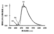
- Compound (1) was dispersed in 2-methyltetrahydrofuran, cooled to 77 K using liquid nitrogen, and then measured for fluorescence and phosphorescence spectra using a spectrofluorometer (Hitachi F-7000).
- the solid line in FIG. 2 is a fluorescence spectrum obtained from 320 nm incident light, and the broken line is a phosphorescence spectrum obtained from 320 nm incident light.
- the peak ends on the short wavelength side of the fluorescence and phosphorescence spectra are defined as S 1 energy and T 1 energy, respectively.
- S 1 energy and T 1 energy are defined as S 1 energy and T 1 energy, respectively.
- compound (1) is a thermally activated delayed fluorescent material that causes reverse intersystem crossing from the T 1 state to the S 1 state at room temperature.
- the position of the peak top of the fluorescence spectrum at 77 K of compound (1) was defined as the experimental value of the emission wavelength.
- the emission wavelength of the compound (1) was 467 nm (position (C) in FIG. 2).
- the S 1 -T 1 energy gap of the compound (1) was evaluated from the quantum chemical calculation according to the following procedures 1 to 4.
- the quantum chemical calculation was performed using 6-31G (d) basis functions for all atoms.
- Gaussian 09 Revision C.01 manufactured by Gaussian was used.
- Procedure 1 Using the density functional theory using the M06-2X functional (hereinafter referred to as “M06-2X method”), the molecular structure that gives the lowest energy within the range of the S 0 state is calculated. the energy was defined as e 0.
- Procedure 2 Calculate the molecular structure that gives the lowest energy within the range of the S 1 state using time-dependent density functional theory using the M06-2X functional (hereinafter referred to as “TD-M06-2X method”). The difference between the lowest energy e 1 and the energy e 0 obtained in the above procedure 1 was defined as E 1 .
- Procedure 3 Using the TD-M06-2X method, calculate the molecular structure having the lowest energy within the range of the T 1 state, and calculate the difference between the lowest energy e 2 and the energy e 0 obtained in the above procedure 1 as E It was defined as 2 .
- Procedure 4 The difference between E 1 and E 2 was defined as “calculated value of S 1 -T 1 energy gap”.
- TD-M06-2X functional is used to calculate the molecular structure that has the lowest energy within the range of the S 1 state, and corresponds to the energy of the difference between the lowest energy e 3 and the energy e 1 obtained in step 2 above.
- the wavelength was defined as “calculated value of emission wavelength”.
- Table 1 shows experimental values and calculated values of the S 1 -T 1 energy gap and emission wavelength of compound (1), and calculated values of emission wavelength of comparative compound (1C).
- the experimental value of the S 1 -T 1 energy gap of the compound (1) was 0.11 eV, and it was experimentally determined to be smaller than 0.24 eV. From this result, it can be seen that the compound (1) causes an inverse intersystem crossing from the T 1 state to the S 1 state at room temperature, that is, a thermally activated delayed fluorescent material.
- the calculated value of the emission wavelength of the compound (1) was longer than the calculated value of the emission wavelength of the comparative compound (1C) in which the cyanopyridine moiety was changed to cyanobenzene.
- the experimental value of the emission wavelength of 1,2,3,5-tetrakis (carbazolo-9-ryl) -4,6-dicyanobenzene (4CzIPN) is 507 nm. It has been reported that the calculated value of the emission wavelength of 4CzIPN determined by the same quantum chemistry calculation as described above is 429 nm, and the calculated value tends to be shorter than the experimental value.
- the experimental value of the emission wavelength of the compound (1) is shorter than the experimental value of the emission wavelength of 4CzIPN, and the calculated value of the emission wavelength of the compound (1) is the experimental value of the emission wavelength of 4CzIPN. Shorter wavelength.
- the calculated emission wavelength of compound (1) is longer than the experimental value of the emission wavelength in 2-methyltetrahydrofuran at 77K.
- the calculated emission wavelength does not accurately represent the absolute value of the experimentally measured emission wavelength, but is useful for relative evaluation of the emission wavelength of a specific compound. You can say that.
- the thermally activated delayed fluorescent material containing cyanopyridine is cyanobenzene. It can be seen that the emission wavelength is longer than that of the light-emitting material contained.
- the calculated value of the S 1 -T 1 energy gap of the compounds (2) and (3) is smaller than that of the compound (1). Therefore, the experimental value of the S 1 -T 1 energy gap of the compounds (2) and (3) is predicted to be smaller than the experimental value of 0.11 eV of the S 1 -T 1 energy gap of the compound (1). Therefore, like the compound (1), the compounds (2) and (3) are considered to cause reverse intersystem crossing from the T 1 state to the S 1 state at room temperature. That is, the compounds (2) and (3) are considered to be thermally activated delayed fluorescent materials.
- the calculated emission wavelength of the compounds (2) and (3) is longer than the calculated emission wavelength of the comparative compounds (2C) and (3C) in which the cyanopyridine moiety is changed to the cyanobenzene moiety.
- the same tendency as in the case of comparison between the compound (1) and the comparative compound (1C) was exhibited.
- the thermally activated delayed fluorescent material containing cyanopyridine has a longer emission wavelength than the light emitting material containing cyanobenzene.
Landscapes
- Chemical & Material Sciences (AREA)
- Organic Chemistry (AREA)
- Engineering & Computer Science (AREA)
- Materials Engineering (AREA)
- Physics & Mathematics (AREA)
- Spectroscopy & Molecular Physics (AREA)
- Electroluminescent Light Sources (AREA)
Abstract
L'invention concerne un élément électroluminescent organique pourvu d'une couche électroluminescente disposée entre une paire d'électrodes. La couche électroluminescente contient un matériau hôte et un matériau dopant fluorescent, et la teneur en matériau fluorescent dopant dans la couche électroluminescente est inférieure ou égale à 49 % de la masse totale de la couche électroluminescente. Le matériau dopant présente une différence entre l'énergie S1 et l'énergie T1 inférieure ou égale à 0,24 eV, et est constitué d'un composé cyanopyridine représenté par la formule générale (I). Dans la formule générale (I), au moins un de R1-R5 représente un groupe cyano, et au moins un de R1-R5 représente un substituant qui n'est ni un atome d'hydrogène ni un groupe cyano.
Priority Applications (1)
| Application Number | Priority Date | Filing Date | Title |
|---|---|---|---|
| JP2015503007A JP6259812B2 (ja) | 2013-02-28 | 2014-02-27 | 有機el素子、ならびにそれを用いた照明器具及びディスプレイ装置 |
Applications Claiming Priority (2)
| Application Number | Priority Date | Filing Date | Title |
|---|---|---|---|
| JP2013038757 | 2013-02-28 | ||
| JP2013-038757 | 2013-02-28 |
Publications (1)
| Publication Number | Publication Date |
|---|---|
| WO2014133062A1 true WO2014133062A1 (fr) | 2014-09-04 |
Family
ID=51428322
Family Applications (1)
| Application Number | Title | Priority Date | Filing Date |
|---|---|---|---|
| PCT/JP2014/054828 Ceased WO2014133062A1 (fr) | 2013-02-28 | 2014-02-27 | Élément électroluminescent organique, et dispositif d'éclairage et dispositif d'affichage utilisant ledit élément |
Country Status (2)
| Country | Link |
|---|---|
| JP (1) | JP6259812B2 (fr) |
| WO (1) | WO2014133062A1 (fr) |
Cited By (20)
| Publication number | Priority date | Publication date | Assignee | Title |
|---|---|---|---|---|
| JP2016110075A (ja) * | 2014-10-03 | 2016-06-20 | 株式会社半導体エネルギー研究所 | 発光装置、モジュール、及び電子機器 |
| WO2019046734A1 (fr) * | 2017-09-01 | 2019-03-07 | Kyulux, Inc. | Composition de matière destinée à être utilisée dans des diodes électroluminescentes organiques |
| JPWO2018155642A1 (ja) * | 2017-02-24 | 2019-12-19 | 国立大学法人九州大学 | 化合物、発光材料および発光素子 |
| US10547014B2 (en) | 2017-06-23 | 2020-01-28 | Kyulux, Inc. | Composition of matter for use in organic light-emitting diodes |
| JP2020510322A (ja) * | 2017-01-16 | 2020-04-02 | 中国科学院長春應用化学研究所 | 青色有機エレクトロルミネッセンスデバイスおよびその製造方法 |
| US10644249B2 (en) | 2017-12-22 | 2020-05-05 | Kyulux, Inc. | Composition of matter for use in organic light-emitting diodes |
| CN111987230A (zh) * | 2019-05-23 | 2020-11-24 | 三星显示有限公司 | 有机发光装置及包括所述有机发光装置的设备 |
| US10892425B1 (en) | 2017-03-03 | 2021-01-12 | Kyulux, Inc. | Composition of matter for use in organic light-emitting diodes |
| US11069860B2 (en) | 2017-08-21 | 2021-07-20 | Kyulux, Inc. | Composition of matter for use in organic light-emitting diodes |
| US11104669B2 (en) | 2018-02-02 | 2021-08-31 | Kyulux, Inc. | Composition of matter for use in organic light-emitting diodes |
| US11283027B1 (en) | 2017-03-03 | 2022-03-22 | Kyulux, Inc. | Composition of matter for use in organic light-emitting diodes |
| US11444250B2 (en) | 2017-12-05 | 2022-09-13 | Kyulux, Inc. | Composition of matter for use in organic light-emitting diodes |
| JP2022140543A (ja) * | 2016-08-19 | 2022-09-26 | 株式会社Kyulux | 有機発光素子 |
| US11498914B2 (en) | 2018-03-30 | 2022-11-15 | Kyulux, Inc. | Composition of matter for use in organic light-emitting diodes |
| CN115368343A (zh) * | 2021-05-18 | 2022-11-22 | 江苏三月科技股份有限公司 | 一种以吡啶衍生物为核心的化合物及其应用 |
| US11542260B2 (en) | 2018-01-31 | 2023-01-03 | Kyulux, Inc. | Composition of matter for use in organic light-emitting diodes |
| US11575088B2 (en) | 2017-12-22 | 2023-02-07 | Kyulux, Inc. | Composition of matter for use in organic light-emitting diodes |
| US11608333B2 (en) | 2018-03-20 | 2023-03-21 | Kyulux, Inc. | Composition of matter for use in organic light-emitting diodes |
| WO2023181958A1 (fr) * | 2022-03-22 | 2023-09-28 | 住友化学株式会社 | Élément électroluminescent et son procédé de production, composé électroluminescent et son procédé de production, composition et son procédé de production, procédé de traitement d'informations, dispositif de traitement d'informations, programme, procédé de fourniture de composé électroluminescent et procédé de génération de données |
| US11778904B2 (en) | 2018-05-09 | 2023-10-03 | Kyulux, Inc. | Composition of matter for use in organic light-emitting diodes |
Families Citing this family (1)
| Publication number | Priority date | Publication date | Assignee | Title |
|---|---|---|---|---|
| JP7153363B2 (ja) * | 2017-12-05 | 2022-10-14 | 株式会社Kyulux | 有機発光ダイオードに用いられる組成物 |
Citations (6)
| Publication number | Priority date | Publication date | Assignee | Title |
|---|---|---|---|---|
| JPH0782552A (ja) * | 1993-09-14 | 1995-03-28 | Nisshinbo Ind Inc | 有機エレクトロルミネッセンス素子 |
| JP2006024830A (ja) * | 2004-07-09 | 2006-01-26 | Sogo Pharmaceutical Co Ltd | 有機エレクトロルミネッセンス素子 |
| JP2008063278A (ja) * | 2006-09-07 | 2008-03-21 | Fujifilm Finechemicals Co Ltd | 1−ピリジン−4−イル−インドール類の製造方法 |
| JP2009094486A (ja) * | 2007-09-18 | 2009-04-30 | Fujifilm Corp | 有機電界発光素子 |
| JP2010114425A (ja) * | 2008-10-10 | 2010-05-20 | Canon Inc | 有機el表示装置 |
| KR20120092909A (ko) * | 2011-02-14 | 2012-08-22 | 에스에프씨 주식회사 | 피리딘 유도체 화합물 및 이를 포함하는 유기전계발광소자 |
-
2014
- 2014-02-27 JP JP2015503007A patent/JP6259812B2/ja active Active
- 2014-02-27 WO PCT/JP2014/054828 patent/WO2014133062A1/fr not_active Ceased
Patent Citations (6)
| Publication number | Priority date | Publication date | Assignee | Title |
|---|---|---|---|---|
| JPH0782552A (ja) * | 1993-09-14 | 1995-03-28 | Nisshinbo Ind Inc | 有機エレクトロルミネッセンス素子 |
| JP2006024830A (ja) * | 2004-07-09 | 2006-01-26 | Sogo Pharmaceutical Co Ltd | 有機エレクトロルミネッセンス素子 |
| JP2008063278A (ja) * | 2006-09-07 | 2008-03-21 | Fujifilm Finechemicals Co Ltd | 1−ピリジン−4−イル−インドール類の製造方法 |
| JP2009094486A (ja) * | 2007-09-18 | 2009-04-30 | Fujifilm Corp | 有機電界発光素子 |
| JP2010114425A (ja) * | 2008-10-10 | 2010-05-20 | Canon Inc | 有機el表示装置 |
| KR20120092909A (ko) * | 2011-02-14 | 2012-08-22 | 에스에프씨 주식회사 | 피리딘 유도체 화합물 및 이를 포함하는 유기전계발광소자 |
Cited By (33)
| Publication number | Priority date | Publication date | Assignee | Title |
|---|---|---|---|---|
| JP2022100311A (ja) * | 2014-10-03 | 2022-07-05 | 株式会社半導体エネルギー研究所 | 発光装置 |
| JP2016110075A (ja) * | 2014-10-03 | 2016-06-20 | 株式会社半導体エネルギー研究所 | 発光装置、モジュール、及び電子機器 |
| JP7381639B2 (ja) | 2014-10-03 | 2023-11-15 | 株式会社半導体エネルギー研究所 | 発光装置 |
| JP7631477B2 (ja) | 2014-10-03 | 2025-02-18 | 株式会社半導体エネルギー研究所 | 発光装置 |
| JP2024020284A (ja) * | 2014-10-03 | 2024-02-14 | 株式会社半導体エネルギー研究所 | 発光装置 |
| US10998750B2 (en) | 2014-10-03 | 2021-05-04 | Semiconductor Energy Laboratory Co., Ltd. | Light-emitting device, module, and electronic device |
| JP2020101802A (ja) * | 2014-10-03 | 2020-07-02 | 株式会社半導体エネルギー研究所 | 発光装置 |
| JP2025072519A (ja) * | 2014-10-03 | 2025-05-09 | 株式会社半導体エネルギー研究所 | 発光装置 |
| JP7290374B2 (ja) | 2016-08-19 | 2023-06-13 | 株式会社Kyulux | 有機発光素子 |
| JP2022140543A (ja) * | 2016-08-19 | 2022-09-26 | 株式会社Kyulux | 有機発光素子 |
| JP2020510322A (ja) * | 2017-01-16 | 2020-04-02 | 中国科学院長春應用化学研究所 | 青色有機エレクトロルミネッセンスデバイスおよびその製造方法 |
| US12120952B2 (en) | 2017-02-24 | 2024-10-15 | Kyulux, Inc. | Compound, light-emitting material and light-emitting element |
| JPWO2018155642A1 (ja) * | 2017-02-24 | 2019-12-19 | 国立大学法人九州大学 | 化合物、発光材料および発光素子 |
| JP7222549B2 (ja) | 2017-02-24 | 2023-02-15 | 株式会社Kyulux | 化合物、発光材料および発光素子 |
| US11283027B1 (en) | 2017-03-03 | 2022-03-22 | Kyulux, Inc. | Composition of matter for use in organic light-emitting diodes |
| US10892425B1 (en) | 2017-03-03 | 2021-01-12 | Kyulux, Inc. | Composition of matter for use in organic light-emitting diodes |
| US10547014B2 (en) | 2017-06-23 | 2020-01-28 | Kyulux, Inc. | Composition of matter for use in organic light-emitting diodes |
| US11069860B2 (en) | 2017-08-21 | 2021-07-20 | Kyulux, Inc. | Composition of matter for use in organic light-emitting diodes |
| WO2019046734A1 (fr) * | 2017-09-01 | 2019-03-07 | Kyulux, Inc. | Composition de matière destinée à être utilisée dans des diodes électroluminescentes organiques |
| US11849634B2 (en) | 2017-09-01 | 2023-12-19 | Kyulux, Inc. | Composition of matter for use in organic light- emitting diodes |
| US11444250B2 (en) | 2017-12-05 | 2022-09-13 | Kyulux, Inc. | Composition of matter for use in organic light-emitting diodes |
| US11575088B2 (en) | 2017-12-22 | 2023-02-07 | Kyulux, Inc. | Composition of matter for use in organic light-emitting diodes |
| US10644249B2 (en) | 2017-12-22 | 2020-05-05 | Kyulux, Inc. | Composition of matter for use in organic light-emitting diodes |
| US11542260B2 (en) | 2018-01-31 | 2023-01-03 | Kyulux, Inc. | Composition of matter for use in organic light-emitting diodes |
| US11104669B2 (en) | 2018-02-02 | 2021-08-31 | Kyulux, Inc. | Composition of matter for use in organic light-emitting diodes |
| US11608333B2 (en) | 2018-03-20 | 2023-03-21 | Kyulux, Inc. | Composition of matter for use in organic light-emitting diodes |
| US11498914B2 (en) | 2018-03-30 | 2022-11-15 | Kyulux, Inc. | Composition of matter for use in organic light-emitting diodes |
| US11778904B2 (en) | 2018-05-09 | 2023-10-03 | Kyulux, Inc. | Composition of matter for use in organic light-emitting diodes |
| JP2020191443A (ja) * | 2019-05-23 | 2020-11-26 | 三星ディスプレイ株式會社Samsung Display Co.,Ltd. | 有機発光素子、及びそれを含む装置 |
| JP7655701B2 (ja) | 2019-05-23 | 2025-04-02 | 三星ディスプレイ株式會社 | 有機発光素子、及びそれを含む装置 |
| CN111987230A (zh) * | 2019-05-23 | 2020-11-24 | 三星显示有限公司 | 有机发光装置及包括所述有机发光装置的设备 |
| CN115368343A (zh) * | 2021-05-18 | 2022-11-22 | 江苏三月科技股份有限公司 | 一种以吡啶衍生物为核心的化合物及其应用 |
| WO2023181958A1 (fr) * | 2022-03-22 | 2023-09-28 | 住友化学株式会社 | Élément électroluminescent et son procédé de production, composé électroluminescent et son procédé de production, composition et son procédé de production, procédé de traitement d'informations, dispositif de traitement d'informations, programme, procédé de fourniture de composé électroluminescent et procédé de génération de données |
Also Published As
| Publication number | Publication date |
|---|---|
| JP6259812B2 (ja) | 2018-01-10 |
| JPWO2014133062A1 (ja) | 2017-02-02 |
Similar Documents
| Publication | Publication Date | Title |
|---|---|---|
| JP6259812B2 (ja) | 有機el素子、ならびにそれを用いた照明器具及びディスプレイ装置 | |
| JP6326251B2 (ja) | 発光材料及びそれを用いた有機el素子 | |
| JP5399418B2 (ja) | 有機電界発光素子 | |
| JP6025959B2 (ja) | 有機発光ダイオードのための2−アザトリフェニレン物質 | |
| TWI429650B (zh) | Organic electroluminescent elements | |
| JP5774267B2 (ja) | 有機エレクトロルミネセント化合物及びこれを使用する発光ダイオード | |
| WO2014129330A1 (fr) | Elément électroluminescent organique, dispositif d'éclairage utilisant celui-ci et dispositif d'affichage | |
| CN104193738B (zh) | 一种基于苯并咪唑的电子传输化合物 | |
| KR102231248B1 (ko) | 유기전기 소자용 화합물, 이를 이용한 유기전기소자 및 그 전자 장치 | |
| WO2010113761A1 (fr) | Dispositif organique électroluminescent | |
| TW201348228A (zh) | 有機電激發光元件用材料及使用其之元件 | |
| KR102413966B1 (ko) | 유기 발광 소자 | |
| TW200418343A (en) | Organic electroluminescent element | |
| TW201343639A (zh) | 有機電激發光元件用材料及使用其之元件 | |
| JP5783749B2 (ja) | エキシマー特性を有する1,8−アリール置換ナフタレン誘導体及びこれを用いた有機el素子 | |
| KR20160095175A (ko) | 유기 전계발광 소자용 재료 및 이것을 사용한 유기 전계발광 소자 | |
| JP2018524379A (ja) | 複素環式化合物、ならびに、電気光学デバイスまたは光電子デバイスにおける複素環式化合物の使用 | |
| JP6580392B2 (ja) | 化合物、混合物、発光層、有機発光素子およびアシストドーパント | |
| CN105622618B (zh) | 有机发光显示装置 | |
| KR20100021367A (ko) | 발광 화합물 및 이를 포함하는 유기전계발광소자 | |
| KR20170016137A (ko) | 유기전기소자용 화합물, 이를 이용한 유기전기소자 및 그 전자 장치 | |
| KR102309763B1 (ko) | 유기전기 소자용 화합물, 이를 이용한 유기전기소자 및 그 전자 장치 | |
| KR102004385B1 (ko) | 신규한 화합물 및 이를 포함하는 유기전계발광소자 | |
| WO2016111196A1 (fr) | Composé, mélange, couche photo-émettrice, élément électroluminescent organique, et dopant auxiliaire | |
| KR102489360B1 (ko) | 유기전기 소자용 화합물, 이를 이용한 유기전기소자 및 그 전자 장치 |
Legal Events
| Date | Code | Title | Description |
|---|---|---|---|
| 121 | Ep: the epo has been informed by wipo that ep was designated in this application |
Ref document number: 14757233 Country of ref document: EP Kind code of ref document: A1 |
|
| ENP | Entry into the national phase |
Ref document number: 2015503007 Country of ref document: JP Kind code of ref document: A |
|
| NENP | Non-entry into the national phase |
Ref country code: DE |
|
| 122 | Ep: pct application non-entry in european phase |
Ref document number: 14757233 Country of ref document: EP Kind code of ref document: A1 |