WO2014136252A1 - Dispositif semi-conducteur - Google Patents
Dispositif semi-conducteur Download PDFInfo
- Publication number
- WO2014136252A1 WO2014136252A1 PCT/JP2013/056407 JP2013056407W WO2014136252A1 WO 2014136252 A1 WO2014136252 A1 WO 2014136252A1 JP 2013056407 W JP2013056407 W JP 2013056407W WO 2014136252 A1 WO2014136252 A1 WO 2014136252A1
- Authority
- WO
- WIPO (PCT)
- Prior art keywords
- current
- power semiconductor
- gate
- circuit
- semiconductor element
- Prior art date
- Legal status (The legal status is an assumption and is not a legal conclusion. Google has not performed a legal analysis and makes no representation as to the accuracy of the status listed.)
- Ceased
Links
Images






Classifications
-
- H—ELECTRICITY
- H03—ELECTRONIC CIRCUITRY
- H03K—PULSE TECHNIQUE
- H03K17/00—Electronic switching or gating, i.e. not by contact-making and –breaking
- H03K17/08—Modifications for protecting switching circuit against overcurrent or overvoltage
- H03K17/082—Modifications for protecting switching circuit against overcurrent or overvoltage by feedback from the output to the control circuit
- H03K17/0822—Modifications for protecting switching circuit against overcurrent or overvoltage by feedback from the output to the control circuit in field-effect transistor switches
-
- H—ELECTRICITY
- H02—GENERATION; CONVERSION OR DISTRIBUTION OF ELECTRIC POWER
- H02M—APPARATUS FOR CONVERSION BETWEEN AC AND AC, BETWEEN AC AND DC, OR BETWEEN DC AND DC, AND FOR USE WITH MAINS OR SIMILAR POWER SUPPLY SYSTEMS; CONVERSION OF DC OR AC INPUT POWER INTO SURGE OUTPUT POWER; CONTROL OR REGULATION THEREOF
- H02M1/00—Details of apparatus for conversion
- H02M1/08—Circuits specially adapted for the generation of control voltages for semiconductor devices incorporated in static converters
- H02M1/088—Circuits specially adapted for the generation of control voltages for semiconductor devices incorporated in static converters for the simultaneous control of series or parallel connected semiconductor devices
-
- H—ELECTRICITY
- H02—GENERATION; CONVERSION OR DISTRIBUTION OF ELECTRIC POWER
- H02M—APPARATUS FOR CONVERSION BETWEEN AC AND AC, BETWEEN AC AND DC, OR BETWEEN DC AND DC, AND FOR USE WITH MAINS OR SIMILAR POWER SUPPLY SYSTEMS; CONVERSION OF DC OR AC INPUT POWER INTO SURGE OUTPUT POWER; CONTROL OR REGULATION THEREOF
- H02M1/00—Details of apparatus for conversion
- H02M1/32—Means for protecting converters other than automatic disconnection
-
- H—ELECTRICITY
- H02—GENERATION; CONVERSION OR DISTRIBUTION OF ELECTRIC POWER
- H02M—APPARATUS FOR CONVERSION BETWEEN AC AND AC, BETWEEN AC AND DC, OR BETWEEN DC AND DC, AND FOR USE WITH MAINS OR SIMILAR POWER SUPPLY SYSTEMS; CONVERSION OF DC OR AC INPUT POWER INTO SURGE OUTPUT POWER; CONTROL OR REGULATION THEREOF
- H02M3/00—Conversion of DC power input into DC power output
- H02M3/02—Conversion of DC power input into DC power output without intermediate conversion into AC
- H02M3/04—Conversion of DC power input into DC power output without intermediate conversion into AC by static converters
- H02M3/10—Conversion of DC power input into DC power output without intermediate conversion into AC by static converters using discharge tubes with control electrode or semiconductor devices with control electrode
- H02M3/145—Conversion of DC power input into DC power output without intermediate conversion into AC by static converters using discharge tubes with control electrode or semiconductor devices with control electrode using devices of a triode or transistor type requiring continuous application of a control signal
- H02M3/155—Conversion of DC power input into DC power output without intermediate conversion into AC by static converters using discharge tubes with control electrode or semiconductor devices with control electrode using devices of a triode or transistor type requiring continuous application of a control signal using semiconductor devices only
- H02M3/156—Conversion of DC power input into DC power output without intermediate conversion into AC by static converters using discharge tubes with control electrode or semiconductor devices with control electrode using devices of a triode or transistor type requiring continuous application of a control signal using semiconductor devices only with automatic control of output voltage or current, e.g. switching regulators
- H02M3/158—Conversion of DC power input into DC power output without intermediate conversion into AC by static converters using discharge tubes with control electrode or semiconductor devices with control electrode using devices of a triode or transistor type requiring continuous application of a control signal using semiconductor devices only with automatic control of output voltage or current, e.g. switching regulators including plural semiconductor devices as final control devices for a single load
-
- H—ELECTRICITY
- H02—GENERATION; CONVERSION OR DISTRIBUTION OF ELECTRIC POWER
- H02M—APPARATUS FOR CONVERSION BETWEEN AC AND AC, BETWEEN AC AND DC, OR BETWEEN DC AND DC, AND FOR USE WITH MAINS OR SIMILAR POWER SUPPLY SYSTEMS; CONVERSION OF DC OR AC INPUT POWER INTO SURGE OUTPUT POWER; CONTROL OR REGULATION THEREOF
- H02M1/00—Details of apparatus for conversion
- H02M1/0003—Details of control, feedback or regulation circuits
- H02M1/0009—Devices or circuits for detecting current in a converter
-
- H—ELECTRICITY
- H03—ELECTRONIC CIRCUITRY
- H03K—PULSE TECHNIQUE
- H03K2217/00—Indexing scheme related to electronic switching or gating, i.e. not by contact-making or -breaking covered by H03K17/00
- H03K2217/0027—Measuring means of, e.g. currents through or voltages across the switch
-
- H—ELECTRICITY
- H10—SEMICONDUCTOR DEVICES; ELECTRIC SOLID-STATE DEVICES NOT OTHERWISE PROVIDED FOR
- H10W—GENERIC PACKAGES, INTERCONNECTIONS, CONNECTORS OR OTHER CONSTRUCTIONAL DETAILS OF DEVICES COVERED BY CLASS H10
- H10W72/00—Interconnections or connectors in packages
- H10W72/071—Connecting or disconnecting
- H10W72/075—Connecting or disconnecting of bond wires
- H10W72/07551—Connecting or disconnecting of bond wires characterised by changes in properties of the bond wires during the connecting
- H10W72/07552—Connecting or disconnecting of bond wires characterised by changes in properties of the bond wires during the connecting changes in structures or sizes
-
- H—ELECTRICITY
- H10—SEMICONDUCTOR DEVICES; ELECTRIC SOLID-STATE DEVICES NOT OTHERWISE PROVIDED FOR
- H10W—GENERIC PACKAGES, INTERCONNECTIONS, CONNECTORS OR OTHER CONSTRUCTIONAL DETAILS OF DEVICES COVERED BY CLASS H10
- H10W72/00—Interconnections or connectors in packages
- H10W72/50—Bond wires
- H10W72/521—Structures or relative sizes of bond wires
- H10W72/527—Multiple bond wires having different sizes
-
- H—ELECTRICITY
- H10—SEMICONDUCTOR DEVICES; ELECTRIC SOLID-STATE DEVICES NOT OTHERWISE PROVIDED FOR
- H10W—GENERIC PACKAGES, INTERCONNECTIONS, CONNECTORS OR OTHER CONSTRUCTIONAL DETAILS OF DEVICES COVERED BY CLASS H10
- H10W72/00—Interconnections or connectors in packages
- H10W72/50—Bond wires
- H10W72/541—Dispositions of bond wires
- H10W72/547—Dispositions of multiple bond wires
- H10W72/5475—Dispositions of multiple bond wires multiple bond wires connected to common bond pads at both ends of the wires
-
- H—ELECTRICITY
- H10—SEMICONDUCTOR DEVICES; ELECTRIC SOLID-STATE DEVICES NOT OTHERWISE PROVIDED FOR
- H10W—GENERIC PACKAGES, INTERCONNECTIONS, CONNECTORS OR OTHER CONSTRUCTIONAL DETAILS OF DEVICES COVERED BY CLASS H10
- H10W72/00—Interconnections or connectors in packages
- H10W72/50—Bond wires
- H10W72/551—Materials of bond wires
- H10W72/552—Materials of bond wires comprising metals or metalloids, e.g. silver
- H10W72/5524—Materials of bond wires comprising metals or metalloids, e.g. silver comprising aluminium [Al]
-
- H—ELECTRICITY
- H10—SEMICONDUCTOR DEVICES; ELECTRIC SOLID-STATE DEVICES NOT OTHERWISE PROVIDED FOR
- H10W—GENERIC PACKAGES, INTERCONNECTIONS, CONNECTORS OR OTHER CONSTRUCTIONAL DETAILS OF DEVICES COVERED BY CLASS H10
- H10W90/00—Package configurations
- H10W90/701—Package configurations characterised by the relative positions of pads or connectors relative to package parts
- H10W90/751—Package configurations characterised by the relative positions of pads or connectors relative to package parts of bond wires
- H10W90/753—Package configurations characterised by the relative positions of pads or connectors relative to package parts of bond wires between laterally-adjacent chips
Definitions
- the present invention relates to a semiconductor device using a power semiconductor element including a current sense cell that obtains a current for current detection by diverting a current flowing through the power semiconductor element.
- the semiconductor device described in Patent Document 1 includes a power semiconductor element, a current detection unit that detects an output current of a current sense cell, an overcurrent limiting circuit, an overcurrent protection circuit, and a drive circuit.
- the overcurrent limiting circuit reduces the gate voltage to a predetermined voltage and limits the current flowing through the power semiconductor element.
- the overcurrent protection circuit turns off the power semiconductor element after a lapse of a predetermined time. That is, the current flowing through the power semiconductor element is limited, and then the power semiconductor element is turned off.
- the ratio of the current sense cell to the main cell may be increased to increase the current flowing from the current sense cell.
- the ratio of the main cells decreases as the ratio of the current sense cells is increased, that is, the efficiency deteriorates, which is not desirable.
- the gate resistance in the drive circuit is increased, the collector voltage of the overcurrent limiting circuit can be lowered, but an increase in the gate resistance leads to an increase in the loss of the semiconductor device, which is not desirable.
- the present invention has been made to solve the above-described problems, and provides a semiconductor device capable of overcurrent protection without increasing loss even in a semiconductor device using a power semiconductor element having a low Vth. With the goal.
- a power semiconductor element that controls a main current flowing between a first electrode and a second electrode by a voltage applied to a gate includes a main cell and a current sense cell, and the current of the main cell is determined by an output current of the current sense cell.
- the overcurrent protection circuit outputs the current sense cell
- a drive circuit for controlling, and a gate current control circuit that is connected between the gate and the drive circuit and controls the output current to be a predetermined constant value; It was.
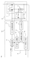
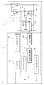
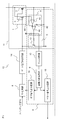
- 1 is a block diagram showing a schematic configuration of a semiconductor device according to a first embodiment of the present invention. It is a block diagram which shows another schematic structure of the semiconductor device by Embodiment 1 of this invention. It is a block diagram which shows another schematic structure of the semiconductor device by Embodiment 1 of this invention. It is a figure which shows the relationship between the gate voltage and drain current of MOSFET as an example of a power semiconductor element.
- 1 is a circuit diagram showing an example of a gate current control circuit of a semiconductor device according to a first embodiment of the present invention. It is a figure which shows an example of the VI characteristic of the gate current control circuit of the semiconductor device by Embodiment 1 of this invention.
- FIG. 6 is a collector current-collector voltage characteristic diagram for explaining the operation of the transistor of the overcurrent limiting circuit. It is a block diagram which shows schematic structure of the semiconductor device by Embodiment 2 of this invention.
- FIG. 1 is a circuit diagram showing a semiconductor device according to Embodiment 1 of the present invention.
- MOSFET 1 Metal Oxide Field Effect Transistor
- IGBT Insulated Gate Bipolar Transistor
- FIG. 1 the free-wheeling diode disposed to face the power semiconductor element 1 is omitted.
- the semiconductor device described here can be used for various power converters such as a three-phase inverter circuit shown in FIG.
- the power semiconductor element 1 has a main cell 2 that mainly conducts current and a current sense cell 3 that shunts current, and a drain terminal and a gate terminal are connected to each other. Between the source of the current sense cell 3 and the source of the main cell 2, a current detection unit 4 that detects the current of the current sense cell 3 is connected. In FIG. 1, as an example of the current detection unit, the current detection unit 4 that converts a current into a voltage using a resistor is illustrated.
- the power semiconductor element to which the present invention is applied is a power semiconductor element having a structure in which the main current flowing between the two electrodes is controlled by the voltage of the gate electrode. .
- the two electrodes through which the main current flows are called the first electrode and the second electrode, respectively.
- the drain is the first electrode and the source is the second electrode.
- the collector is the first electrode and the emitter is the second electrode.
- the first electrode of the main cell and the first electrode of the current sense cell are connected.
- the second electrode of the current sense cell and the second electrode of the main cell have a structure that can be electrically connected to the outside separately.
- a current detection unit 4 is connected between the second electrode of the current sense cell and the second electrode of the main cell.
- FIG. 2 shows an example of the current detection unit 4 different from FIG.
- the voltage across the current detection resistor 41 and the voltage of the reference voltage source 42 are compared by the comparator 40. If the voltage across the current detection resistor 41 is larger, the output of the comparator 40 becomes high impedance, and the current detection unit 4 has a high output. Output a signal. Since the short circuit current detection level is set by the comparator 40 and the reference voltage source 42, it is an advantage that the accuracy is higher than that of the current detection unit 4 including only the resistance shown in FIG.
- FIG. 3 shows still another example of the current detection unit 4.
- the inverting input terminal of the operational amplifier 43 is connected to the source of the current sense cell 3, and the non-inverting input terminal is connected to the source of the main cell 2.
- a resistor 44 is connected between the inverting input terminal and the output terminal. Since the output voltage of the operational amplifier 43 is proportional to the output current of the current sense cell 3, the comparator 40 compares the output voltage of the operational amplifier 43 with the reference voltage source 42. If the reference voltage source 42 is larger, the output of the comparator 40 has a high impedance. Thus, the current detection unit 4 outputs a high output signal.
- the advantages of this method are as follows.
- the voltage between the inverting input terminal and the non-inverting input terminal of the operational amplifier 43 becomes zero, the gate-source voltage and the drain-source voltage of the main cell 2 and the current sense cell 3 become equal. Therefore, the current ratio between the current sense cell 3 and the main cell 2 is equal to the ratio of the number of cells, and current detection with high accuracy is possible.
- the output signal of the current detector 4 is input to the overcurrent limiting circuit 5.
- the overcurrent limiting circuit 5 receives this signal and reduces the gate voltage of the MOSFET 1. If the gate voltage decreases, the drain current flowing through the MOSFET 1 also decreases, and the MOSFET 1 is protected from overcurrent. In this state, the output from the drive circuit 6 is still output, and the current controlled by the gate current control circuit 14 flows to the transistor 13 of the overcurrent limiting circuit 5. In FIG. 1 to FIG. 3, one transistor is used as the overcurrent limiting circuit 5.
- the present invention is not limited to this configuration.
- the output signal of the current detection unit 4 is amplified after using a plurality of transistors. The gate voltage of the semiconductor element 1 may be reduced.
- a filter circuit 10 is inserted between the current detection unit 4 and the overcurrent detection circuit 9.
- a power semiconductor module 11 including a current detection unit 4, an overcurrent limiting circuit 5, a MOSFET 1, a control circuit 12 including a drive circuit 6, an overcurrent detection circuit 9, and the like are included.
- a noise removal filter circuit 10 between the power semiconductor module 11 and the control circuit 12. Since the overcurrent detection signal is delayed by the filter circuit 10, the overcurrent limiting circuit 5 is required to have a function of limiting the drain current to the extent that the drain current becomes substantially zero so that the MOSFET 1 is not destroyed.
- FIG. 4 shows the relationship between the gate voltage and drain current of a MOSFET which is an example of a power semiconductor element.
- a power semiconductor element having a high threshold voltage Vth and a large change in drain current is targeted. Therefore, in order not to lower the gate voltage more than necessary, the gate voltage at the time of protection is adjusted by connecting a Zener diode between the gate of the MOSFET and the collector of the transistor 13 of the overcurrent limiting circuit 5.
- a MOSFET having a low Vth shown in FIG. 4 is also targeted. Therefore, the gate voltage at the time of protection needs to be lowered to the voltage indicated by the reduced target gate voltage, and the Zener diode is omitted.
- An element such as a diode or a resistor may be inserted for protection between the gate of the MOSFET and the collector of the transistor 13 of the overcurrent limiting circuit 5, but the voltage drop due to this protection element is 2 V or less. What should I do?
- the signal from the current detection unit 4 is input to the filter circuit 10 and is input to the overcurrent detection circuit 9 after a certain delay time.
- the overcurrent detection circuit 9 compares the output signal of the current detection unit 4 with the overcurrent set value, and outputs a signal to the error signal output circuit 15 and the off command output circuit 16 if it is determined as an overcurrent.
- the off command output circuit 16 outputs an off command to the drive circuit 6, and the output from the drive circuit 6 is turned off. Along with this, the current flowing through the transistor 13 of the overcurrent limiting circuit 5 also decreases.
- the control current value of the gate current control circuit 14 is set to the gate current value during the mirror period during normal operation.
- the current value flowing out of the drive circuit is controlled by the control current value of the gate current control circuit 14 not only when switching in normal operation but also when the overcurrent limiting circuit 5 operates when the arm is short-circuited or the load is short-circuited. Since the switching time is determined by the gate current value in the mirror period, the gate current control circuit 14 controls the gate current value to be a predetermined constant value, that is, the gate current value in the mirror period during normal operation of the power semiconductor element 1. However, the switching loss does not increase.
- FIG. 14 A configuration example of the gate current control circuit 14 is shown in FIG.
- the current flowing through the resistor 19 is small and the transistor 18 remains off, so that the transistor 17 is turned on and the gate current is not controlled.
- the current flowing through the resistor 19 increases, the transistor 18 is turned on, the emitter-base voltage of the transistor 17 decreases, and the gate current is controlled to a predetermined constant value. That is, the current flowing through the resistor 19 is controlled so that the voltage drop due to the resistor 19 becomes equal to the emitter-base voltage that turns on the transistor 18. Since there is no circuit for controlling the gate current other than the gate current control circuit 14 between the drive circuit 6 and the gate of the power semiconductor element 1, the gate current is controlled to a predetermined constant value.
- the output current of the gate current control circuit 14 is a predetermined constant value, that is, the mirror period during the normal operation of the power semiconductor element 1.
- the gate current value is controlled.
- a low resistance that does not significantly affect the gate current value in the mirror period may be connected between the drive circuit 6 and the gate of the power semiconductor element 1. .
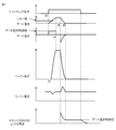
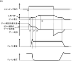
- Fig. 7 shows the sequence of protection operation when the output of the circuit of Fig. 1 is in a short-circuit state.
- the gate current becomes a predetermined constant current. Since the gate current is constant, the gate voltage rises with a constant slope.
- the gate voltage exceeds the threshold (timing of t1) the drain current starts to be energized.
- the value of the gate voltage reaches the power supply voltage of the drive circuit 6 (timing at t4), the gate voltage and the drain current become constant and the gate current becomes zero. Since the circuit is in a short circuit state, an overcurrent flows, and the overcurrent limiting operation starts from the timing t5.
- the current flowing from the drive circuit 6 into the transistor 13 of the overcurrent limiting circuit 5 is controlled by the gate current control circuit 14 to a predetermined constant value.
- a discharge current from the gate of the MOSFET 1 is also superimposed on the transistor 13 of the overcurrent limiting circuit 5, but since the current flowing from the drive circuit 6 is controlled to a predetermined constant value by the gate current control circuit 14, the transistor 13 Is kept at a low value, and the gate voltage of MOSFET 1 can be reduced to almost zero at the timing of t6.
- FIG. 7 it can be seen that if the current flowing from the drive circuit 6 to the transistor 13 of the overcurrent limiting circuit 5 is limited, the gate voltage when the overcurrent is limited can be significantly reduced.
- the circuit shown in FIG. 8 has the same configuration as the circuit of FIG. 1 except that it does not include the gate current control circuit 14 but includes the gate resistor 7.
- the gate resistor 7 has an effect of limiting the gate current, the current value depends on the voltage value applied to both ends of the gate resistor 7. That is, the potential on the drive circuit side of the gate resistor 7 does not change, and the gate voltage of the MOSFET 1 changes, so that the voltage value applied across the gate resistor 7 changes and the gate current also changes.
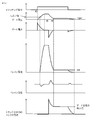
- FIG. 9 shows switching waveforms during normal switching of the circuit of the comparative example of FIG.
- the gate current decreases, and becomes a constant current value during the period from t2 to t3.
- the period from t2 to t3 in which the gate current is constant is called a mirror period, and the switching speed is determined by the gate current in the mirror period.
- the mirror voltage at the rated current of the power semiconductor element 1 is about 11V.
- the change of the drain voltage ends at the timing of t3
- the mirror period also ends, the gate voltage rises again, and rises to the power supply voltage of the drive circuit 6 at the timing of t4.
- the drain current increases as the gate voltage increases. Since a current proportional to the drain current flows through the current sense cell 3, a signal proportional to the drain current is output from the current detection unit 4.
- the base current of the transistor 13 of the overcurrent limiting circuit 5 increases according to the signal from the current detection unit 4, the collector voltage of the transistor 13 begins to decrease at the timing t5, and the gate voltage of the MOSFET 1 decreases. The current also decreases to Id1 at the timing of t6. As shown in FIG.
- the collector voltage Vce of the transistor 13 is determined to be Vgs1 from the static characteristics of the transistor 13 and the circuit characteristics shown in the following equation.
- Ic (Vcc ⁇ Vce) / Rg (3)
- Ic is the collector current of the transistor 13
- Vce is the collector voltage of the transistor 13
- Vcc is the power supply voltage of the drive circuit 6
- Rg is the gate resistor 7 in the drive circuit 6.
- the gate current represented by the equation (1) is applied to the transistor 13 of the overcurrent limiting circuit 5.
- the current must be close to the maximum value. From the comparison between Expression (1) and Expression (2), it can be seen that the transistor 13 must pass a current that is nearly four times the gate current in the mirror period.
- the ratio of the current sense cell 3 to the main cell 2 is increased and the current flowing from the current sense cell 3 is increased.
- the ratio of the current sense cell 3 is increased, the ratio of the main cell 2 is decreased, that is, the efficiency is deteriorated, which is not desirable.
- a current sense cell is provided in a plurality of MOSFET chips, in addition to deteriorating efficiency, a current is extracted from the current sense cell of each chip. Wiring needs to be performed, and wiring in the power semiconductor module increases, which is undesirable from the viewpoint of miniaturization and design freedom.
- FIG. 11 shows the static characteristics and the operating state of the transistor 13 of the overcurrent limiting circuit 5.
- the horizontal axis represents the collector voltage Vce of the transistor 13
- the vertical axis represents the collector current Ic.
- the characteristics of Ic-Vce are shown using the base current of the transistor 13 as a parameter.
- the diagonal straight line indicates the circuit characteristic in the circuit of the comparative example shown in FIG. 8, that is, the equation (3).
- the intersection of the static characteristic determined by the base current and this oblique straight line is the operating point of the transistor 13. For example, if the base current during overcurrent protection is Ib0, the collector voltage of the transistor 13 is Vce2.
- the gate resistance Rg in the drive circuit is increased, the intercept of the vertical axis of the straight line determined from the circuit constant in FIG. 11 can be lowered, and the collector voltage of the overcurrent limiting circuit can be lowered.
- An increase in gate resistance is undesirable because it leads to an increase in the loss of the semiconductor device.
- a gate current control circuit 14 is provided as shown in FIGS.
- the gate current control circuit 14 controls the output current so as to be a predetermined constant value, that is, the gate current value in the mirror period during normal operation of the power semiconductor element 1.
- the predetermined constant value may not be exactly the same as the gate current value during normal operation of the power semiconductor element 1, and may be a value in the range of 90% to 110% of the gate current value during normal operation. .
- the collector current of the transistor 13 of the overcurrent limiting circuit 5 is close to one-fourth of the collector current at the time of overcurrent limitation in the comparative example.
- the collector voltage of the transistor 13 can be suppressed to a value indicated by Vce1, for example, even when the same base current flows.
- Vce1 the gate voltage of the MSFET 1 during the overcurrent protection operation is kept low as Vce1 shown in FIG. Therefore, it is possible to reliably protect against overcurrent.
- the power semiconductor element in the present invention may be formed of silicon.
- a wide band gap semiconductor having a larger band gap than silicon may be used.
- the wide band gap semiconductor include silicon carbide, a gallium nitride-based material, and diamond.
- the effect obtained by the present invention is increased.
- the power semiconductor element formed of a wide band gap semiconductor has a high withstand voltage and a high allowable current density, the power semiconductor element can be downsized. By using these miniaturized power semiconductor elements, a semiconductor device incorporating these elements can be miniaturized.
- the wide band gap semiconductor has high heat resistance, it is possible to reduce the size of the heatsink fins and the air cooling of the water cooling part, thereby further reducing the size of the semiconductor device. Furthermore, since the power loss is low, it is possible to increase the efficiency of the power semiconductor element, and further increase the efficiency of the semiconductor device.
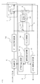
- FIG. FIG. 12 is a circuit diagram showing a semiconductor device according to the second embodiment of the present invention. 12, the same reference numerals as those in FIG. 1 denote the same or corresponding parts.
- a latch circuit 20 is added to the circuit shown in FIG.
- the overcurrent protection circuit 8 operates to reduce the current of the power semiconductor element 1.
- the current detection value in the current detection unit 4 also decreases, so the input to the overcurrent limit circuit 5 also decreases, and the collector voltage of the transistor 13 of the overcurrent limit circuit 5 increases.
- the latch circuit 20 does not decrease the output to the transistor 13 for a predetermined time even if the current detection value decreases once the current detection unit 4 detects a current exceeding a predetermined threshold value determined to be an overcurrent. That is, it is a circuit that performs a latch operation.
- the latch circuit 20 particularly when a gate current control circuit is provided for a power semiconductor element having a low threshold voltage, an increase and a decrease in the current of the power semiconductor element 1 can be prevented.
- a semiconductor device capable of performing a current protection operation can be provided.
- FIG. 13 is a circuit diagram showing a three-phase inverter circuit as an example of a power converter to which the semiconductor device of the present invention is applied.
- the circuit in FIG. 13 is a power converter that converts alternating current into direct current, switches the converted direct current to convert it into three-phase alternating current, and drives the motor M.
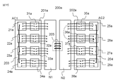
- a plurality of power semiconductor elements are connected in parallel to the upper arms 100a, 100b, and 100c and the lower arms 200a, 200b, and 200c, respectively. Details of the upper arm 100a and the lower arm 200a are shown in FIG. The details will be described by taking the lower arm 200a as an example.
- Each of the IGBTs 21a to 28a as a power semiconductor element and a set of diodes 31a to 38a connected in parallel to the respective IGBTs are connected in parallel. Furthermore, eight sets of diodes connected in parallel with the IGBT are mounted by connecting two modules each having four sets of diodes connected in parallel with the IGBT on the substrate 201a and the substrate 202a in parallel. ing.
- FIG. 15 shows a plan view of a schematic configuration for mounting the lower arm 200a.
- the collectors which are the first electrodes of the IGBTs 21a to 24a, are arranged on the substrate 201a on which the copper pattern is formed so that each first electrode is connected to the copper pattern.
- the emitters which are the second electrodes of the IGBTs 21a to 24a, are directly connected to each other by the aluminum wire wiring 203 without a member other than a power semiconductor element such as a copper pattern or a diode.
- the emitters that are the second electrodes of the IGBTs 25a to 28a arranged on the substrate 202a are also connected to each other by the aluminum wire wiring 204 without any member other than the power semiconductor element such as a copper pattern or a diode.
- a current sense cell is provided in only one IGBT among the IGBTs 21a to 28a, and an emitter as a second electrode of the current sense cell is connected to the current detection unit 4 separately.
- the impedance between the emitters is the impedance of the path indicated by the broken line through the terminal block N1 and the terminal block N2.
- the impedance between the emitters becomes an impedance of a short path by the aluminum wire wirings 203 and 204, and the impedance is reduced.
- the gate voltage of each IGBT can be reduced equally.
- a power semiconductor element with a low threshold voltage such as a wide band gap semiconductor, has a difference in emitter potential unless the emitters are connected by an aluminum wire wiring.
- a state occurs in which the voltage is equal to or higher than the threshold voltage and the gate voltage of some power semiconductor elements is equal to or lower than the threshold voltage, and an overcurrent continues to flow through the power semiconductor element having a high gate voltage. Further, by connecting the left and right terminal blocks N1 and N2 with the short aluminum wire wiring 205, the impedance between the IGBT emitters of the left and right substrates 201a and 202a is reduced, and the same effect is obtained.
- the gate current control circuit 5 of the present invention when the gate current control circuit 5 of the present invention is provided for a power semiconductor element having a low threshold voltage such as a wide band gap semiconductor, the mounting structure as described above ensures reliable connection in parallel. There is an effect that an overcurrent protection operation can be performed on all power semiconductor elements.
- the IGBT is described as an example of the power semiconductor element, but the same applies to the case where the power semiconductor element is a MOSFET.
Landscapes
- Engineering & Computer Science (AREA)
- Power Engineering (AREA)
- Electronic Switches (AREA)
- Power Conversion In General (AREA)
Abstract
L'invention concerne un dispositif semi-conducteur qui comprend un circuit de protection contre les surintensités (8) pour protéger, par détection d'un courant d'une cellule principale (2) à l'aide d'un courant de sortie d'une cellule de détection de courant (3), un élément semi-conducteur de puissance (1) dans les cas où un courant de l'élément semi-conducteur de puissance (1) devient une surintensité. Le circuit de protection contre les surintensités (8) est configuré de telle sorte que le circuit de protection contre les surintensités comprend : une section de détection de courant (4) qui détecte le courant de sortie de la cellule de détection de courant ; un circuit de limitation de surintensité (5) qui réduit une tension à appliquer sur une grille correspondant à des signaux de sortie de la section de détection de courant (4) ; un circuit d'attaque (6) pour commander l'allumage/extinction de l'élément semi-conducteur de puissance (1) par commande de la tension à appliquer à la grille ; et un circuit de commande de courant de grille (14), qui est connecté entre la grille et le circuit d'attaque (6), et qui réalise une commande de telle sorte que le courant de sortie est à une valeur constante prédéterminée.
Priority Applications (2)
| Application Number | Priority Date | Filing Date | Title |
|---|---|---|---|
| JP2015504080A JP5940211B2 (ja) | 2013-03-08 | 2013-03-08 | 半導体装置 |
| PCT/JP2013/056407 WO2014136252A1 (fr) | 2013-03-08 | 2013-03-08 | Dispositif semi-conducteur |
Applications Claiming Priority (1)
| Application Number | Priority Date | Filing Date | Title |
|---|---|---|---|
| PCT/JP2013/056407 WO2014136252A1 (fr) | 2013-03-08 | 2013-03-08 | Dispositif semi-conducteur |
Publications (1)
| Publication Number | Publication Date |
|---|---|
| WO2014136252A1 true WO2014136252A1 (fr) | 2014-09-12 |
Family
ID=51490810
Family Applications (1)
| Application Number | Title | Priority Date | Filing Date |
|---|---|---|---|
| PCT/JP2013/056407 Ceased WO2014136252A1 (fr) | 2013-03-08 | 2013-03-08 | Dispositif semi-conducteur |
Country Status (2)
| Country | Link |
|---|---|
| JP (1) | JP5940211B2 (fr) |
| WO (1) | WO2014136252A1 (fr) |
Cited By (7)
| Publication number | Priority date | Publication date | Assignee | Title |
|---|---|---|---|---|
| WO2016174756A1 (fr) * | 2015-04-30 | 2016-11-03 | 三菱電機株式会社 | Circuit de protection et système à circuit de protection |
| WO2017026367A1 (fr) * | 2015-08-07 | 2017-02-16 | 三菱電機株式会社 | Appareil commutateur de puissance |
| CN108063612A (zh) * | 2016-11-09 | 2018-05-22 | 富士电机株式会社 | 半导体装置 |
| CN109667694A (zh) * | 2017-10-17 | 2019-04-23 | 富士电机株式会社 | 半导体装置 |
| JP2019515558A (ja) * | 2016-09-20 | 2019-06-06 | ミツビシ・エレクトリック・アールアンドディー・センター・ヨーロッパ・ビーヴィMitsubishi Electric R&D Centre Europe B.V. | スイッチングを制御する装置及び方法 |
| JP2021040218A (ja) * | 2019-09-02 | 2021-03-11 | 株式会社東芝 | スイッチ回路 |
| CN113169659A (zh) * | 2018-12-11 | 2021-07-23 | 三菱电机株式会社 | 电力用半导体元件的驱动电路以及使用其的电力用半导体模块 |
Families Citing this family (3)
| Publication number | Priority date | Publication date | Assignee | Title |
|---|---|---|---|---|
| KR102456560B1 (ko) * | 2020-08-25 | 2022-10-19 | (주) 트리노테크놀로지 | 쇼트서킷 내량이 강화된 전력 반도체 소자 |
| CN113241940B (zh) * | 2021-07-12 | 2021-09-10 | 上海芯龙半导体技术股份有限公司 | 一种过流保护电路及开关电源芯片 |
| JP7732280B2 (ja) | 2021-08-27 | 2025-09-02 | 富士電機株式会社 | 半導体モジュール |
Citations (3)
| Publication number | Priority date | Publication date | Assignee | Title |
|---|---|---|---|---|
| JPH05267580A (ja) * | 1992-03-24 | 1993-10-15 | Fuji Electric Co Ltd | 半導体装置 |
| JP2009060358A (ja) * | 2007-08-31 | 2009-03-19 | Denso Corp | 過電流保護回路及び電力変換システム |
| WO2010134276A1 (fr) * | 2009-05-19 | 2010-11-25 | 三菱電機株式会社 | Circuit d'attaque de la grille |
-
2013
- 2013-03-08 JP JP2015504080A patent/JP5940211B2/ja active Active
- 2013-03-08 WO PCT/JP2013/056407 patent/WO2014136252A1/fr not_active Ceased
Patent Citations (3)
| Publication number | Priority date | Publication date | Assignee | Title |
|---|---|---|---|---|
| JPH05267580A (ja) * | 1992-03-24 | 1993-10-15 | Fuji Electric Co Ltd | 半導体装置 |
| JP2009060358A (ja) * | 2007-08-31 | 2009-03-19 | Denso Corp | 過電流保護回路及び電力変換システム |
| WO2010134276A1 (fr) * | 2009-05-19 | 2010-11-25 | 三菱電機株式会社 | Circuit d'attaque de la grille |
Cited By (17)
| Publication number | Priority date | Publication date | Assignee | Title |
|---|---|---|---|---|
| WO2016174756A1 (fr) * | 2015-04-30 | 2016-11-03 | 三菱電機株式会社 | Circuit de protection et système à circuit de protection |
| US10629587B2 (en) | 2015-04-30 | 2020-04-21 | Mitsubishi Electric Corporation | Protection circuit and protection circuit system |
| US10651839B2 (en) | 2015-08-07 | 2020-05-12 | Mitsubishi Electric Corporation | Power switching apparatus |
| WO2017026367A1 (fr) * | 2015-08-07 | 2017-02-16 | 三菱電機株式会社 | Appareil commutateur de puissance |
| CN107980199A (zh) * | 2015-08-07 | 2018-05-01 | 三菱电机株式会社 | 电源开关装置 |
| JPWO2017026367A1 (ja) * | 2015-08-07 | 2018-05-10 | 三菱電機株式会社 | パワースイッチング装置 |
| DE112016003609B4 (de) | 2015-08-07 | 2020-07-09 | Mitsubishi Electric Corporation | Energie-Schaltvorrichtung |
| CN107980199B (zh) * | 2015-08-07 | 2020-03-27 | 三菱电机株式会社 | 电源开关装置 |
| JP2019515558A (ja) * | 2016-09-20 | 2019-06-06 | ミツビシ・エレクトリック・アールアンドディー・センター・ヨーロッパ・ビーヴィMitsubishi Electric R&D Centre Europe B.V. | スイッチングを制御する装置及び方法 |
| CN108063612A (zh) * | 2016-11-09 | 2018-05-22 | 富士电机株式会社 | 半导体装置 |
| CN108063612B (zh) * | 2016-11-09 | 2024-03-08 | 富士电机株式会社 | 半导体装置 |
| CN109667694A (zh) * | 2017-10-17 | 2019-04-23 | 富士电机株式会社 | 半导体装置 |
| CN109667694B (zh) * | 2017-10-17 | 2022-04-15 | 富士电机株式会社 | 半导体装置 |
| CN113169659A (zh) * | 2018-12-11 | 2021-07-23 | 三菱电机株式会社 | 电力用半导体元件的驱动电路以及使用其的电力用半导体模块 |
| CN113169659B (zh) * | 2018-12-11 | 2023-08-04 | 三菱电机株式会社 | 电力用半导体元件的驱动电路以及使用其的电力用半导体模块 |
| JP2021040218A (ja) * | 2019-09-02 | 2021-03-11 | 株式会社東芝 | スイッチ回路 |
| JP7199325B2 (ja) | 2019-09-02 | 2023-01-05 | 株式会社東芝 | スイッチ回路 |
Also Published As
| Publication number | Publication date |
|---|---|
| JP5940211B2 (ja) | 2016-06-29 |
| JPWO2014136252A1 (ja) | 2017-02-09 |
Similar Documents
| Publication | Publication Date | Title |
|---|---|---|
| JP5940211B2 (ja) | 半導体装置 | |
| JP5289580B2 (ja) | 半導体装置 | |
| JP6045611B2 (ja) | ゲート駆動回路 | |
| US9013850B2 (en) | Semiconductor device | |
| JP5783997B2 (ja) | 電力用半導体装置 | |
| US8710894B2 (en) | Circuit arrangement having a load transistor and a voltage limiting circuit and method for driving a load transistor | |
| JP6380953B2 (ja) | 電子回路 | |
| JP2012090435A (ja) | 駆動回路及びこれを備える半導体装置 | |
| JPWO2019038957A1 (ja) | 制御回路および電力変換装置 | |
| JP5925364B2 (ja) | 電力用半導体装置 | |
| CN110739941B (zh) | 半导体装置 | |
| JP7537183B2 (ja) | 半導体装置 | |
| JP2018061301A (ja) | 半導体駆動装置ならびにそれを用いた電力変換装置 | |
| CN113056864B (zh) | 电力转换装置 | |
| JP2017118807A (ja) | 電力変換システム、パワーモジュールおよび半導体装置 | |
| JP2009165285A (ja) | 半導体装置 | |
| JPWO2012043146A1 (ja) | 半導体装置 | |
| JP6168899B2 (ja) | パワーモジュール | |
| JP6590437B2 (ja) | 半導体電力変換装置 | |
| WO2024261949A1 (fr) | Dispositif d'attaque à semi-conducteur et dispositif de conversion d'énergie électrique | |
| JPH06105448A (ja) | 保護機能を備えたスイッチ装置 | |
| CN120185592A (zh) | 开关元件控制装置 | |
| JP2003023769A (ja) | 電力用半導体モジュール | |
| CN107534015A (zh) | 保护电路及保护电路系统 | |
| JP2023046512A (ja) | 半導体装置 |
Legal Events
| Date | Code | Title | Description |
|---|---|---|---|
| 121 | Ep: the epo has been informed by wipo that ep was designated in this application |
Ref document number: 13877099 Country of ref document: EP Kind code of ref document: A1 |
|
| ENP | Entry into the national phase |
Ref document number: 2015504080 Country of ref document: JP Kind code of ref document: A |
|
| NENP | Non-entry into the national phase |
Ref country code: DE |
|
| 122 | Ep: pct application non-entry in european phase |
Ref document number: 13877099 Country of ref document: EP Kind code of ref document: A1 |