WO2015121908A1 - 漏電検出部及び漏電遮断器 - Google Patents
漏電検出部及び漏電遮断器 Download PDFInfo
- Publication number
- WO2015121908A1 WO2015121908A1 PCT/JP2014/006202 JP2014006202W WO2015121908A1 WO 2015121908 A1 WO2015121908 A1 WO 2015121908A1 JP 2014006202 W JP2014006202 W JP 2014006202W WO 2015121908 A1 WO2015121908 A1 WO 2015121908A1
- Authority
- WO
- WIPO (PCT)
- Prior art keywords
- conductor
- phase
- load
- zero
- current transformer
- Prior art date
- Legal status (The legal status is an assumption and is not a legal conclusion. Google has not performed a legal analysis and makes no representation as to the accuracy of the status listed.)
- Ceased
Links
Images









Classifications
-
- H—ELECTRICITY
- H01—ELECTRIC ELEMENTS
- H01H—ELECTRIC SWITCHES; RELAYS; SELECTORS; EMERGENCY PROTECTIVE DEVICES
- H01H83/00—Protective switches, e.g. circuit-breaking switches, or protective relays operated by abnormal electrical conditions otherwise than solely by excess current
- H01H83/14—Protective switches, e.g. circuit-breaking switches, or protective relays operated by abnormal electrical conditions otherwise than solely by excess current operated by imbalance of two or more currents or voltages, e.g. for differential protection
- H01H83/144—Protective switches, e.g. circuit-breaking switches, or protective relays operated by abnormal electrical conditions otherwise than solely by excess current operated by imbalance of two or more currents or voltages, e.g. for differential protection with differential transformer
-
- H—ELECTRICITY
- H01—ELECTRIC ELEMENTS
- H01H—ELECTRIC SWITCHES; RELAYS; SELECTORS; EMERGENCY PROTECTIVE DEVICES
- H01H83/00—Protective switches, e.g. circuit-breaking switches, or protective relays operated by abnormal electrical conditions otherwise than solely by excess current
- H01H83/20—Protective switches, e.g. circuit-breaking switches, or protective relays operated by abnormal electrical conditions otherwise than solely by excess current operated by excess current as well as by some other abnormal electrical condition
- H01H83/22—Protective switches, e.g. circuit-breaking switches, or protective relays operated by abnormal electrical conditions otherwise than solely by excess current operated by excess current as well as by some other abnormal electrical condition the other condition being imbalance of two or more currents or voltages
- H01H83/226—Protective switches, e.g. circuit-breaking switches, or protective relays operated by abnormal electrical conditions otherwise than solely by excess current operated by excess current as well as by some other abnormal electrical condition the other condition being imbalance of two or more currents or voltages with differential transformer
-
- H—ELECTRICITY
- H01—ELECTRIC ELEMENTS
- H01H—ELECTRIC SWITCHES; RELAYS; SELECTORS; EMERGENCY PROTECTIVE DEVICES
- H01H83/00—Protective switches, e.g. circuit-breaking switches, or protective relays operated by abnormal electrical conditions otherwise than solely by excess current
- H01H83/14—Protective switches, e.g. circuit-breaking switches, or protective relays operated by abnormal electrical conditions otherwise than solely by excess current operated by imbalance of two or more currents or voltages, e.g. for differential protection
- H01H83/144—Protective switches, e.g. circuit-breaking switches, or protective relays operated by abnormal electrical conditions otherwise than solely by excess current operated by imbalance of two or more currents or voltages, e.g. for differential protection with differential transformer
- H01H2083/148—Protective switches, e.g. circuit-breaking switches, or protective relays operated by abnormal electrical conditions otherwise than solely by excess current operated by imbalance of two or more currents or voltages, e.g. for differential protection with differential transformer with primary windings formed of rigid copper conductors
Definitions
- the present invention relates to a leakage detection unit that is disposed between a power source and a load and detects a leakage on the load side, and a leakage breaker that interrupts an electric circuit at the time of leakage, and is particularly suitable when a zero-phase current transformer is used for leakage detection. Is.
- the zero-phase current transformer penetrates all phases of current through the annular core, and if a so-called secondary current occurs in the annular core, it is assumed that a leakage (ground fault) has occurred.
- the earth leakage circuit breaker allows the current between the power source and the load to pass through the annular core.
- the earth leakage breaker is connected to the earth leakage trip device for breaking the electric circuit when the electric leakage is detected by the electric leakage detection unit equipped with the electric leakage detection circuit, and when the overcurrent (short circuit) occurs on the load side, Generally equipped with an overcurrent trip device to cut off.
- the leakage trip device or the overcurrent trip device opens the contact of the power supply side circuit in the switching mechanism to cut off the electric circuit.
- an earth leakage circuit breaker and an earth leakage detection part there exist some which are described in the following patent document 1 and patent document 2, for example.
- a plate-like power supply side conductor corresponding to each phase of the power supply side circuit is arranged on one side in the axial direction of the zero-phase current transformer.
- the plate-shaped load side conductor corresponding to each phase of a load side terminal is arrange
- the round bar-shaped through conductors for all phases are passed through the annular core of the zero-phase current transformer and abut against the corresponding power supply side conductor and load side conductor.
- the power supply side conductor and the load side conductor are connected to each phase in a state of passing through the zero-phase current transformer, so that the gap between the conductors of each phase is filled with an insulating resin such as silicon or epoxy and cured. And ensure insulation between each phase.
- the plate-like power supply side conductor and the plate-like load side conductor are continuously integrated into a bifurcated shape with a plate-like through conductor, and a coating process is performed for each phase. Insulate with. Then, these conductor members are inserted so as to straddle the annular core of the zero-phase current transformer, and the circuit is assembled.
- both the leakage detection unit described in Patent Document 1 and the leakage detection unit described in Patent Document 2 have room for improvement in assembly.
- the leakage detection unit described in Patent Document 1 since it is necessary to fill the insulating resin in a state where the power-side conductor and the load-side conductor of each phase are connected by the through conductor, all the conductors are accurately Need to be positioned. In addition, if bubbles or cracks occur in the filled insulating resin, the insulation is impaired, so it is necessary to prevent them from occurring.
- the leakage detection part described in the said patent document 2 since it is necessary to insert the conductor member formed in the forked shape so that the annular core of a zero phase current transformer may be straddled, the assembly itself is troublesome.
- the formation of these conductor members is also complicated. Further, in order to insert the bifurcated conductor member into the annular core, it is necessary to enlarge the inner hole of the annular core. As a result, there is a possibility that the zero-phase current transformer and the leakage detection unit are also enlarged.
- the present invention has been made to solve these various problems, and provides a leakage detector and a leakage breaker that are easy to process a conductor member, enable downsizing of the device, and are particularly excellent in assembling. It is intended.
- the leakage detection unit arranges the load-side conductor corresponding to each phase of the load-side terminal in any one of the axial directions of the zero-phase current transformer.
- the power supply side conductor corresponding to each phase of a power supply side circuit is arrange
- a penetration conductor part is continuously fixed to either one of a load side conductor and a power source side conductor about one phase or two phases among these load side conductors and a power source side conductor.
- the through conductor portion is continuously fixed to either the load side conductor or the power source side conductor.
- through conductor portions penetrate through the annular core of the zero-phase current transformer and are joined to any joint portion of the load side conductor and the power source side conductor that correspond in phase and are not continuously fixed. Furthermore, an insulating coating portion is applied to the outside of the through conductor portion continuous fixing portion of at least the load side conductor and the power source side conductor in which the through conductor portion is continuously fixed.
- the zero-phase current transformer axis orthogonal cross-sectional shape of the through conductor is a fan shape.
- the annular core of the zero-phase current transformer is oval, it is desirable that the zero-phase current transformer axis orthogonal cross-sectional shape of the through conductor is a combination of a sector shape and a square shape.
- a leakage breaker includes a contact opening / closing mechanism, an overcurrent tripping device, and a leakage tripping device for a power supply circuit in a main body case.
- the leakage trip device is configured by combining a leakage detection unit and a trip coil unit. Then, the leakage detecting unit arranges the load-side conductor corresponding to each phase of the load-side terminal in any one of the axial directions of the zero-phase current transformer.
- the power supply side conductor corresponding to each phase of a power supply side circuit is arrange
- a penetration conductor part is continuously fixed to either one of a load side conductor and a power source side conductor about one phase or two phases among these load side conductors and a power source side conductor.
- the through conductor portion is continuously fixed to either the load side conductor or the power source side conductor.
- These through conductor portions penetrate through the annular core of the zero-phase current transformer and are joined to any joint portion of the load side conductor and the power source side conductor that correspond in phase and are not continuously fixed.
- an insulating coating portion is applied to the outside of the through conductor portion continuous fixing portion of at least the load side conductor and the power source side conductor in which the through conductor portion is continuously fixed.
- the through-conductor portion that is continuously fixed passes through the annular core from one or the other of the zero-phase current transformers in the axial direction.
- the conductor is disposed on one side in the axial direction of the zero-phase current transformer, and the power supply side conductor is disposed on the other side in the axial direction of the zero-phase current transformer.
- the through conductor portion is joined to any joint portion of the load side conductor and the power source side conductor that correspond to each other and are not continuously fixed. Therefore, the load side conductor and the power source side conductor are connected to each phase. Is done.
- the insulation coating portion is applied to the outside of the through conductor portion continuous fixing portion of the load side conductor and the power source side conductor, insulation is ensured between the load side conductor or the power source side conductor adjacent to the joint portion. It becomes possible to do. Therefore, it is excellent in assemblability, and it is not necessary to enlarge the inner hole of the annular core of the zero-phase current transformer, so that the apparatus can be downsized.
- the load side conductor and power supply side conductor with a through-conductor part are comprised, for example with the combination of a plate-like load side conductor and power supply side conductor, and a rod-like through conductor part, processing of a conductor member is easy. .
- the inner-phase part of the annular core is made to be It can be effectively used as a penetrating part.
- the inner-hole portion of the annular core is obtained by combining the cross-sectional shape of the through-conductor section perpendicular to the axis of the zero-phase current transformer with a sector shape and a square shape. Can be effectively utilized as the through portion of the through conductor portion. Further, by interposing an insulating plate member between the joints close to each other in one or both of the axial directions of the zero-phase current transformer, the joints close to each other can be easily and reliably insulated. be able to.
- FIG. 3 is a front view of a leakage detection unit in FIG. 2.
- FIG. 3 is a plan view of a leakage detection unit in FIG. 2.
- FIG. 3 is an assembly diagram of a leakage detection unit in FIG. 2. It is explanatory drawing of the continuous fixation part of a power supply side conductor or a load side conductor, and a penetration conductor part. It is explanatory drawing of the joining state of the power supply side conductor of T phase, and a load side conductor.
- FIG. 1 is a perspective view showing the overall configuration of the earth leakage breaker of the present embodiment.
- the earth leakage circuit breaker includes a main body case 1 made of a molded resin case and a cover that covers the main body case 1, and the illustration of the cover is omitted in FIG. 1.
- This earth leakage circuit breaker is provided with a contact opening / closing mechanism 3 of the power circuit 2, an overcurrent tripping device 4, and an earth leakage tripping device 5 on the inner side of the main body case 1, and a known arc extinguishing device for a current breaking unit. 21 and an operation handle 22 are also mounted.
- the overcurrent trip device 4 is an overcurrent trip device using a known current transformer.
- the leakage trip device 5 includes a leakage detection unit 6 and a trip coil unit 7. As in the conventional case, the leakage trip device 5 opens the contact point of the switching mechanism 3 with the trip coil unit 7 and interrupts the electric circuit when leakage is detected by the leakage detection unit 6.
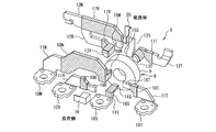
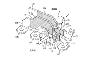
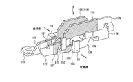
- FIG. 2 is a perspective view of the leakage detection unit 6 of the leakage breaker of FIG. 1
- FIG. 3 is a front view of the leakage detection unit 6 of FIG. 2
- FIG. 4 is a plan view of the leakage detection unit 6 of FIG.
- FIG. 5 is an assembly diagram of the leakage detection unit 6 of FIG.
- the leakage detection unit 6 of the present embodiment includes a zero-phase current transformer 8 as in the prior art, and the annular core 9 is a true circle. Therefore, the inner hole of the annular core 9 is also a perfect circle.
- the secondary wiring of the zero phase current transformer 8 is not shown.
- the power supply side circuit 2 of the present embodiment is a four-pole circuit in which an N-phase is added to three general T-phase, S-phase, and R-phase.
- the load-side terminal of the leakage detection unit 6 is also provided for four poles of the T-phase load-side terminal 10T, the S-phase load-side terminal 10S, the R-phase load-side terminal 10R, and the N-phase load-side terminal 10N.
- these load-side terminals 10T to 10N have a rectangular plate shape.
- one side of the zero-phase current transformer 8 is in the axial direction, and in the figure, the zero-phase current transformer is below the front side. 8 are arranged side by side in a direction orthogonal to the axial direction.
- load side terminals 10T to 10N plate-like load side conductors 11T to 11N are continuously fixed in the vertical direction of FIG. 2 on the annular core 9 side of the zero-phase current transformer 8.
- the load side terminals 10T to 10N and the load side conductors 11T to 11N may be integrally formed by bending a series of plate conductors.
- These load-side conductors 11T to 11N are arranged on one side of the zero-phase current transformer 8 in the axial direction.
- the ends of the load side conductors 11T to 11N opposite to the load side terminals 10T to 10N are arranged so as to be concentrated in the inner hole portion of the annular core 9. For example, as shown in FIG.
- the load-side conductors 11T to 11N are arranged such that the T-phase load-side conductor 11T is shown in the upper right in the figure, the S-phase load-side conductor 11S is shown in the lower-right, and the R-phase.
- the load-side conductor 11R is arranged at the lower left in the figure, and the N-phase load-side conductor 11N is arranged at the upper left in the figure. Therefore, these load-side conductors 11T to 11N have few overlapping portions in the axial direction of the zero-phase current transformer 8, and reduce the dimension in the axial direction of the zero-phase current transformer 8 in their layout. Can do.
- the power supply side conductors 12T to 12N corresponding to the respective phases of the power supply side circuit 2 are arranged on the other side in the axial direction of the zero-phase current transformer 8, as shown in FIG.
- These power supply side conductors 12T to 12N are formed by bending, for example, a plate-like conductor, and one end thereof is arranged so as to be concentrated in the inner hole portion of the annular core 9.
- the other ends of the power supply side conductors 12T to 12N are connected to the respective phases of the power supply side circuit 2 (not shown).
- one end portions of the power supply side conductors 12T to 12N collected in the inner hole portion of the annular core 9 are opposed to the end portions of the corresponding load side conductors 11T to 11N, respectively. Therefore, for example, as shown in FIG. 14 when FIG. 2 is viewed from the back side, the T-phase power supply side conductor 12T is illustrated in the upper left, the S phase power supply side conductor 12S is illustrated in the lower left, and the R phase power supply side The conductor 12R is arranged at the lower right in the figure, and the N-phase power supply side conductor 12N is arranged at the upper right in the figure. Therefore, these power supply side conductors 12T to 12N have few overlapping portions in the axial direction of the zero-phase current transformer 8, and reduce the dimension in the axial direction of the zero-phase current transformer 8 in their layout. Can do.
- the T phase power supply side conductor 12T and the R phase power supply side conductor 12R which are positioned diagonally with respect to the inner hole of the annular core 9, are each provided with a T phase power supply side through conductor portion 13T.
- the R-phase power supply side through conductor portion 13R is continuously fixed.
- the S-phase load-side conductor 11S and the N-phase load-side conductor 11N which are positioned diagonally with respect to the inner hole of the annular core 9, are respectively S-phase load-side through conductor portions 14S.
- the N-phase load side through conductor portion 14N is continuously fixed.
- the T-phase power supply side through conductor portion 13T and the R phase power supply side through conductor portion 13R penetrate the annular core 9 from the end portions on the annular core 9 side of the T phase power supply side conductor 12T and the R phase power supply side conductor 12R, respectively. Projecting so that it is continuously fixed. Further, the S-phase load side through conductor portion 14S and the N-phase load side through conductor portion 14N penetrate the annular core 9 from the end portions on the annular core 9 side of the S-phase load side conductor 11S and the N-phase load side conductor 11N, respectively. So as to protrude continuously.
- the S-phase power-side conductor 12S and the N-phase power-side conductor 12N which are located diagonally with respect to the inner hole of the annular core 9, are respectively provided with S-shaped ends.
- the phase power supply side junction 15S and the N phase power supply side junction 15N are integrally formed.
- T-phase load-side conductor 11T and R-phase load-side conductor 11R which are located diagonally with respect to the inner hole of the annular core 9, are respectively provided at the end portions on the annular core 9 side.
- the phase load side junction 16T and the R phase load side junction 16R are integrally formed.
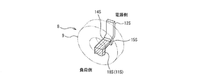
- a continuous fixing structure of the N phase load side through conductor portion 14N to the N phase load side conductor 11N is shown in FIG.
- a fan-shaped central conductor having a central angle of 90 ° that is, a cylindrical through conductor portion 14N vertically divided into 1 ⁇ 4
- the central angle of the sector is located at the center of the inner hole of the annular core 9.
- the outer peripheral surface of the through-conductor part 14N which consists of the 1/4 cylinder is joined to the annular core 9 side edge part of the load side conductor 11N, and both are integrally fixed continuously by soldering or welding, for example.
- the power supply side insulation coating portions 17T to 17N are provided outside the power supply side conductors 12T to 12N except the S phase power supply side conductor 12S. Further, load-side insulating coating portions 18T to 18N are provided outside the load-side conductors 11T to 11N. These insulating coating portions are formed integrally with each conductor member, for example, by injection molding an insulating resin on the outside of the conductor member.
- the N phase power supply side insulation coating portion 17N is not applied to the N phase power supply side junction portion 15N.
- the T phase load side insulation coating portion 18T and the R phase load side insulation coating portion 18R are respectively connected to the T phase load side junction portion 16T and the R phase load side junction portion 16R. Not given.
- the T phase power supply side insulation coating portion 17T and the R phase power supply side insulation coating portion 17R are respectively the T phase power supply side through conductor portion 13T and the R phase power supply side through conductor portion. It is given to the continuous fixed part to the power supply side conductor of 13R.
- the S phase load side insulating coating portion 18S and the N phase load side insulating coating portion 18N are respectively an S phase load side through conductor portion 14S and an N phase load side through conductor portion. It is given to the continuous fixed part to the load side conductor of 14N.
- the T-phase power supply side insulation coating portion 17T and the R-phase power supply side insulation coating portion 17R are not applied to the protruding tip portions of the T-phase power supply side through conductor portion 13T and the R phase power supply side through conductor portion 13R, respectively.
- the S-phase load-side insulating coating portion 18S and the N-phase load-side insulating coating portion 18N are not applied to the projecting tip portions of the S-phase load-side through conductor portion 14S and the N-phase load-side through conductor portion 14N, respectively. .
- FIG. 7 is an explanatory diagram of a joining state of the T-phase power supply side through conductor portion 13T of the T-phase power supply conductor 12T and the T-phase load-side joint portion 16T of the T-phase load-side conductor 11T.
- the T-phase power supply side insulating coating portion 17T is not applied to the protruding tip portion of the T-phase power supply side through conductor portion 13T. Further, the T-phase load side insulating coating portion 18T is not applied to the T-phase load side joint portion 16T. Therefore, when the T-phase power supply side through conductor portion 13T is joined to the T-phase load side junction portion 16T, the T-phase power supply side conductor 12T and the T-phase load side conductor 11T penetrate the annular core 9 of the zero-phase current transformer 8. Electrically connected.
- FIG. 8 is an explanatory diagram of the joining state of the S-phase load-side through conductor portion 14S of the S-phase load-side conductor 11S and the S-phase power-source-side joint 15S of the S-phase power-source-side conductor 12S.
- the S-phase load-side insulating coating portion 18S is not applied to the protruding tip portion of the S-phase load-side through conductor portion 14S. Further, the S-phase power supply side insulating coating portion is not applied to the S-phase power supply side conductor 12S itself. Therefore, when the S-phase load-side through conductor portion 14S is joined to the S-phase power source-side joint portion 15S, the S-phase power source-side conductor 12S and the S-phase load-side conductor 11S pass through the annular core 9 of the zero-phase current transformer 8. Electrically connected.
- FIG. 9 is an explanatory diagram of a joining state of the R-phase power-side through conductor portion 13R of the R-phase power-side conductor 12R and the R-phase load-side joint portion 16R of the R-phase load-side conductor 11R.
- the R-phase power-side insulating coating portion 17R is not applied to the protruding tip of the R-phase power-side through conductor portion 13R. Further, the R-phase load side insulating coating portion 18R is not applied to the R-phase load side joint portion 16R. Therefore, when the R-phase power supply side through conductor portion 13R is joined to the T-phase load side junction portion 16R, the R-phase power supply-side conductor 12R and the R-phase load-side conductor 11R pass through the annular core 9 of the zero-phase current transformer 8. Electrically connected.
- FIG. 10 is an explanatory diagram of the joining state of the N-phase load-side through conductor portion 14N of the N-phase load-side conductor 11N and the N-phase power source-side joint 15N of the N-phase power source-side conductor 12N.
- the N-phase load-side insulating coating portion 18N is not applied to the protruding tip portion of the N-phase load-side through conductor portion 14N. Further, the N phase power supply side insulating coating portion 17N is not applied to the N phase power supply side junction 15N. Therefore, when the N-phase load side through conductor portion 14N is joined to the N-phase power source side joint portion 15N, the N-phase power source side conductor 12N and the N-phase load side conductor 11N penetrate the annular core 9 of the zero-phase current transformer 8. Electrically connected.
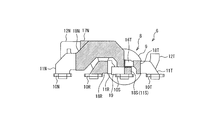
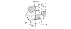
- FIG. 15 shows that among the power supply side conductors 12T to 12N and the load side conductors 11T to 11N thus connected, the T phase power supply side conductor 12T and the T phase load side conductor 11T, and the N phase power supply side conductors 12N and N A state in the annular core 9 of the phase load side conductor 11N is shown as a representative.
- the quarter-phase T-phase power supply side through conductor portion 13T and the N phase load side through conductor portion 14N are adjacent to each other in the inner hole of the annular core 9 as shown in the figure.
- the T-phase power supply side insulation coating portion 17T and the N-phase load side insulation coating portion 18N are applied to at least the continuous fixation portion with the T-phase power supply side conductor 12T and the continuous fixation portion with the N-phase load side conductor 11N, respectively. Therefore, a sufficient insulation length is secured in the axial direction of the zero-phase current transformer 8.
- the T-phase load-side joint 16T and the R-phase load-side joint 16R located at diagonal positions are close to each other.
- the S-phase power supply side junction 15S and the N-phase power supply side junction 15N located at diagonal positions are close to each other.
- the T-phase load-side insulating coating portion 18T is not applied to the T-phase load-side bonding portion 16T
- the R-phase load-side insulating coating portion 18R is not applied to the R-phase load-side bonding portion 16R.
- the S-phase power supply side conductor 12S is not provided with the S-phase power supply-side insulation coating portion itself
- the N-phase power supply-side junction 15N is not provided with the N-phase power supply-side insulation coating portion 17N.
- the load-side insulating plate member 19 is inserted from the load side between the T-phase load-side joint 16T and the R-phase load-side joint 16R that are close to each other.
- the insulation between the phase load side junction 16T and the R phase load side junction 16R is ensured.
- the load-side insulating plate member 19 is made of, for example, an insulating resin and is formed in a box shape that completely covers the R-phase load-side joint portion 16R in the present embodiment. Therefore, as shown in FIG.
- a load-side insulating plate member 19 is interposed between the adjacent T-phase load-side joint 16T and R-phase load-side joint 16R, and the T-phase load-side joint 16T and R Insulation is secured between the phase load side joints 16R.
- the power supply side insulating plate member 20 is inserted from the power supply side between the S phase power supply side joint 15 ⁇ / b> S and the N phase power supply side joint 15 ⁇ / b> N that are close to each other. Insulation is secured between the S-phase power supply side junction 15S and the N-phase power supply side junction 15N.
- the power supply side insulating plate member 20 is made of, for example, an insulating resin, and is formed in a box shape that completely covers the N-phase power supply side joint portion 15N in the present embodiment. Therefore, as shown in FIG.
- the power supply side insulating plate member 20 is interposed between the adjacent S phase power supply side junction 15 ⁇ / b> S and the N phase power supply side junction 15 ⁇ / b> N, and the S phase power supply side junction 15 ⁇ / b> S and N Insulation is secured between the phase power supply side junctions 15N.
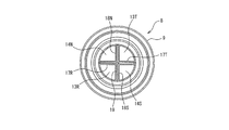
- FIG. 16 shows a state of the power supply side through conductor portions 13T and 13R and the load side through conductor portions 14S and 14N in the annular core 9 of the zero-phase current transformer 8.
- the power supply side through conductor portions 13T and 13R and the load side through conductor portions 14S and 14N having a 1 ⁇ 4 cylindrical shape and a sector cross section with a central angle of 90 ° are used, they interfere with each other. And efficiently accommodated in the inner hole of the annular core 9.
- the power-side insulating coating portions 17T and 17R are provided outside the power-side through conductor portions 13T and 13R, and the load-side insulating coating portions 18S and 18N are provided outside the load-side through conductor portions 14S and 14N. Therefore, insulation is also secured.
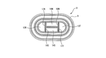
- FIG. 17 shows an example of the power supply side through conductor portions 13T and 13R and the load side through conductor portions 14S and 14N when the inner hole of the annular core 9 of the zero phase current transformer 8 is oval.
- the inner hole of the annular core 9 is a perfect circle. Therefore, the four-pole penetrating conductor portion may be a sector-shaped section having a quarter cylindrical shape and a central angle of 90 °.
- the through conductor portion is efficiently accommodated in the inner hole of the annular core 9 by simply combining the through conductor portions having a fan-shaped cross section. Not.
- the through conductor portions 14S and 14N that are continuously fixed are arranged from one side in the axial direction of the zero phase current transformer 8, and the through conductor portions 13T and 13R are arranged in the axial direction of the zero phase current transformer 8.
- the load-side conductors 11T to 11N are arranged on one side in the axial direction of the zero-phase current transformer 8 so as to alternately pass through the annular core 9, and the power-side conductors 12T to 12N are arranged to the zero-phase current transformer. 8 is arranged on the other side in the axial direction.
- the through conductor portions 13T, 13R, 14S, and 14N have phases corresponding to each other and the joint portions 16T and 16R of the load side conductors 11T and 11R and the joint portions 15S and 15N of the power source side conductors 12S and 12N that are not continuously fixed. Therefore, the power supply side conductors 12T to 12N and the load side conductors 11T to 11N are connected for each phase.
- the insulating coating portions 18S, 18N, and 17R are provided at least outside the through conductor portion continuous fixing portions of the load side conductors 11S and 11N and the power source side conductor 12R, the joint portions 16T, 16R, 15S, and 15N are provided.
- the load-side conductors 11S, 11N and the power-side conductors 12T, 12R with the through-conductor portions 14S, 14N, 13T, 13R are, for example, plate-like load-side conductors 11S, 11N and power-side conductors 12T, 12R and rod-like penetrations. Since it is configured in combination with the conductor portions 14S, 14N, 13T, and 13R, the conductor member can be easily processed.
- the annular core 9 of the zero-phase current transformer 8 is a perfect circle
- the zero-phase current transformer axis orthogonal cross-sectional shape of the through conductor portions 14S, 14N, 13T, and 13R is fan-shaped, 9 inner hole portions can be effectively utilized as the through portions of the through conductor portions 14S, 14N, 13T, and 13R.
- the annular core 9 of the zero-phase current transformer 8 is oval
- the cross-sectional shape of the through-phase conductor portions 14S, 14N, 13T, and 13R is orthogonal to the combination of a sector and a quadrangle.
- annular core 9 can be effectively utilized as a penetration part of penetration conductor part 14S, 14N, 13T, 13R.
- the insulating plate members 19 and 20 are interposed between the joint portions 15S, 15N, 16T, and 16R that are close to each other, thereby being close to each other.
- the joint portions 15S, 15N, 16T, and 16R can be easily and reliably insulated.
- the T-phase, S-phase, R-phase, and N-phase through conductor portions are alternately inserted from the power supply side and the load side.
- the approach area of the junction part which adjoins by the side of a power supply or a load can be made small.
- the four-pole through conductor portions do not necessarily have to be inserted alternately. In that case, there is a possibility that the approach area of the joints close to each other may become large. In such a case, there is no problem if insulation is ensured by interposing an insulating plate member.
- the pole number of an electric circuit is T, S, and R-phase. Even 3 poles are acceptable.
- either one of the through conductors is inserted into the annular core from either the power source side or the load side, and the remaining through conductors are inserted into the annular core from either the power source side or the load side. Plug it into.
Landscapes
- Engineering & Computer Science (AREA)
- Power Engineering (AREA)
- Transformers For Measuring Instruments (AREA)
- Breakers (AREA)
Abstract
Description
本発明はこれらの諸問題を解決すべくなされたものであり、導体部材の加工が容易で、装置の小型化を可能とし、特に組立性に優れた漏電検出部及び漏電遮断器を提供することを目的とするものである。
また、この漏電検出部において、零相変流器の環状コアが長円形である場合には、貫通導体部の零相変流器軸直交断面形状を扇形と四角形との組合せとすることが望ましい。
また、この漏電検出部において、前記零相変流器の軸方向の何れか一方又は双方で、互いに近接する前記接合部の間に絶縁板部材を介装することが望ましい。
また、零相変流器の環状コアが長円形である場合には、貫通導体部の零相変流器軸直交断面形状を扇形と四角形との組合せとすることにより、環状コアの内孔部を貫通導体部の貫通部として有効に活用することができる。
また、零相変流器の軸方向の何れか一方又は双方で、互いに近接する接合部の間に絶縁板部材を介装することで、互いに近接する接合部を容易にして且つ確実に絶縁することができる。
前記貫通導体部のうち、N相負荷側貫通導体部14NのN相負荷側導体11Nへの連続固定構造を代表して図6に示す。本実施形態では、例えば中心角が90°の扇形、つまり1/4に縦割りした円柱状の貫通導体部14Nを用い、扇形の中心角が環状コア9の内孔の中心に位置するようにして配置する。そして、その1/4円柱からなる貫通導体部14Nの外周面を負荷側導体11Nの環状コア9側端部に接合し、例えば半田付けや溶接によって両者を一体的に連続固定する。なお、貫通導体部14Nが予め一体的に連続固定した状態で形成された負荷側導体11Nを用いることも可能である。
また、零相変流器8の環状コア9が長円形である場合には、貫通導体部14S、14N、13T、13Rの零相変流器軸直交断面形状を扇形と四角形との組合せとすることにより、環状コア9の内孔部を貫通導体部14S、14N、13T、13Rの貫通部として有効に活用することができる。
また、零相変流器8の軸方向の何れか一方又は双方で、互いに近接する接合部15S、15N、16T、16Rの間に絶縁板部材19、20を介装することで、互いに近接する接合部15S、15N、16T、16Rを容易にして且つ確実に絶縁することができる。
また、前記実施形態では、T、S、R相の3極にN相を加えた4極の漏電検出部及び漏電遮断器について詳述したが、電路の極数はT、S、R相の3極であっても差し支えない。その場合は、何れか1極の貫通導体部を電源側及び負荷側の何れか一方から環状コア内に差し込み、残りの極の貫通導体部を電源側及び負荷側の何れか他方から環状コア内に差し込むようにすればよい。
2 電源側回路
3 開閉機構
4 過電流引外し装置
5 漏電引外し装置
6 漏電検出部
7 トリップコイルユニット
8 零相変流器
9 環状コア
10T~10N 負荷側端子
11T~11N 負荷側導体
12T~12N 電源側導体
13T、13R 電源側貫通導体部
14S、14N 負荷側貫通導体部
15S、15N 電源側接合部
16T、16R 負荷側接合部
17T~17N 電源側絶縁コーティング部
18T~18N 負荷側絶縁コーティング部
19 負荷側絶縁板部材
20 電源側絶縁板部材
Claims (5)
- 環状コアを有する零相変流器と、負荷側端子の各相に対応して前記零相変流器の軸方向の何れか一方に配置される負荷側導体と、電源側回路の各相に対応して前記零相変流器の軸方向の何れか他方に配置される電源側導体と、一相又は二相については前記負荷側導体及び電源側導体の何れか一方に連続固定され、残りの相については前記負荷側導体及び電源側導体の何れか他方に連続固定され、前記零相変流器の環状コアを貫通して、相が対応し且つ連続固定されていない前記負荷側導体及び電源側導体の何れかの接合部に接合される貫通導体部と、少なくとも前記貫通導体部が連続固定されている前記負荷側導体及び電源側導体の当該貫通導体部連続固定部の外側に施された絶縁コーティング部とを備えた漏電検出部。
- 前記零相変流器の環状コアが真円形である場合、前記貫通導体部の零相変流器軸直交断面形状が扇形であることを特徴とする請求項1に記載の漏電検出部。
- 前記零相変流器の環状コアが長円形である場合、前記貫通導体部の零相変流器軸直交断面形状が扇形と四角形との組合せであることを特徴とする請求項1に記載の漏電検出部。
- 前記零相変流器の軸方向の何れか一方又は双方で、互いに近接する前記接合部の間に絶縁板部材を介装したことを特徴とする請求項1乃至3の何れか一項に記載の漏電検出部。
- 電源側回路の接点の開閉機構、過電流引外し装置、漏電引外し装置を本体ケース内に搭載し、前記漏電引外し装置は、漏電検出部、トリップコイルユニットを組合せて構成される多極形の漏電遮断器であって、前記漏電検出部は、環状コアを有する零相変流器と、負荷側端子の各相に対応して前記零相変流器の軸方向の何れか一方に配置される負荷側導体と、前記電源側回路の各相に対応して前記零相変流器の軸方向の何れか他方に配置される電源側導体と、一相又は二相については前記負荷側導体及び電源側導体の何れか一方に連続固定され、残りの相については前記負荷側導体及び電源側導体の何れか他方に連続固定され、前記零相変流器の環状コアを貫通して、相が対応し且つ連続固定されていない前記負荷側導体及び電源側導体の何れかの接合部に接合される貫通導体部と、少なくとも前記貫通導体部が連続固定されている前記負荷側導体及び電源側導体の当該貫通導体部連続固定部の外側に施された絶縁コーティング部とを備えたことを特徴とする漏電遮断器。
Priority Applications (3)
| Application Number | Priority Date | Filing Date | Title |
|---|---|---|---|
| JP2015562574A JP6065128B2 (ja) | 2014-02-17 | 2014-12-12 | 漏電検出部及び漏電遮断器 |
| CN201480043766.6A CN105474347B (zh) | 2014-02-17 | 2014-12-12 | 漏电检测单元和漏电断路器 |
| EP14882559.9A EP3109884B1 (en) | 2014-02-17 | 2014-12-12 | Leakage current detection unit and leakage current breaker |
Applications Claiming Priority (2)
| Application Number | Priority Date | Filing Date | Title |
|---|---|---|---|
| JP2014-027858 | 2014-02-17 | ||
| JP2014027858 | 2014-02-17 |
Publications (1)
| Publication Number | Publication Date |
|---|---|
| WO2015121908A1 true WO2015121908A1 (ja) | 2015-08-20 |
Family
ID=53799680
Family Applications (1)
| Application Number | Title | Priority Date | Filing Date |
|---|---|---|---|
| PCT/JP2014/006202 Ceased WO2015121908A1 (ja) | 2014-02-17 | 2014-12-12 | 漏電検出部及び漏電遮断器 |
Country Status (4)
| Country | Link |
|---|---|
| EP (1) | EP3109884B1 (ja) |
| JP (1) | JP6065128B2 (ja) |
| CN (1) | CN105474347B (ja) |
| WO (1) | WO2015121908A1 (ja) |
Cited By (2)
| Publication number | Priority date | Publication date | Assignee | Title |
|---|---|---|---|---|
| CN108574160A (zh) * | 2018-06-01 | 2018-09-25 | 浙江中凯科技股份有限公司 | 一种控制与保护开关电器的导电装置 |
| CN108766846A (zh) * | 2018-07-09 | 2018-11-06 | 中国电力科学研究院有限公司 | 一种带有漏电保护功能的智能费控限流断路器装置及保护方法 |
Families Citing this family (2)
| Publication number | Priority date | Publication date | Assignee | Title |
|---|---|---|---|---|
| CN107907714B (zh) * | 2017-07-14 | 2019-12-24 | 国网浙江省电力公司湖州供电公司 | 一种多功能漏电检测器具 |
| JP7289100B2 (ja) * | 2019-07-22 | 2023-06-09 | パナソニックIpマネジメント株式会社 | 漏電保護装置、及び分電盤 |
Citations (4)
| Publication number | Priority date | Publication date | Assignee | Title |
|---|---|---|---|---|
| JPS4873717U (ja) * | 1971-12-18 | 1973-09-13 | ||
| JPS50151311U (ja) * | 1974-05-31 | 1975-12-16 | ||
| JPH05114523A (ja) * | 1991-10-22 | 1993-05-07 | Fuji Electric Co Ltd | 零相変流器1次導体の絶縁構造 |
| JPH10321116A (ja) * | 1997-05-19 | 1998-12-04 | Fuji Electric Co Ltd | 漏電遮断器の漏洩電流検出構造 |
Family Cites Families (7)
| Publication number | Priority date | Publication date | Assignee | Title |
|---|---|---|---|---|
| FR2711838B1 (fr) * | 1993-10-25 | 1996-01-05 | Legrand Sa | Boîtier de tore, et tore bobiné comportant un tel boîtier. |
| FR2772979B1 (fr) * | 1997-12-18 | 2002-09-20 | Schneider Electric Sa | Dispositif de raccordement electrique d'un bloc differentiel sur un disjoncteur ou analogue et bloc differentiel equipe d'un tel dispositif |
| ES2164593B1 (es) * | 2000-03-17 | 2003-05-16 | Ge Power Controls Iberica S L | Dispositivo de deteccion de fuga a tierra. |
| CN2473740Y (zh) * | 2001-04-29 | 2002-01-23 | 锡山市宏泰电器有限责任公司 | 一种剩余电流断路器中的互感机构 |
| JP4502318B2 (ja) * | 2004-06-02 | 2010-07-14 | 河村電器産業株式会社 | 漏電遮断器 |
| JP4736949B2 (ja) * | 2006-05-23 | 2011-07-27 | 富士電機機器制御株式会社 | 漏電遮断器 |
| CN202905448U (zh) * | 2012-11-12 | 2013-04-24 | 常熟开关制造有限公司(原常熟开关厂) | 零序电流互感器主回路固定结构 |
-
2014
- 2014-12-12 WO PCT/JP2014/006202 patent/WO2015121908A1/ja not_active Ceased
- 2014-12-12 CN CN201480043766.6A patent/CN105474347B/zh active Active
- 2014-12-12 EP EP14882559.9A patent/EP3109884B1/en active Active
- 2014-12-12 JP JP2015562574A patent/JP6065128B2/ja active Active
Patent Citations (4)
| Publication number | Priority date | Publication date | Assignee | Title |
|---|---|---|---|---|
| JPS4873717U (ja) * | 1971-12-18 | 1973-09-13 | ||
| JPS50151311U (ja) * | 1974-05-31 | 1975-12-16 | ||
| JPH05114523A (ja) * | 1991-10-22 | 1993-05-07 | Fuji Electric Co Ltd | 零相変流器1次導体の絶縁構造 |
| JPH10321116A (ja) * | 1997-05-19 | 1998-12-04 | Fuji Electric Co Ltd | 漏電遮断器の漏洩電流検出構造 |
Cited By (2)
| Publication number | Priority date | Publication date | Assignee | Title |
|---|---|---|---|---|
| CN108574160A (zh) * | 2018-06-01 | 2018-09-25 | 浙江中凯科技股份有限公司 | 一种控制与保护开关电器的导电装置 |
| CN108766846A (zh) * | 2018-07-09 | 2018-11-06 | 中国电力科学研究院有限公司 | 一种带有漏电保护功能的智能费控限流断路器装置及保护方法 |
Also Published As
| Publication number | Publication date |
|---|---|
| JP6065128B2 (ja) | 2017-01-25 |
| CN105474347B (zh) | 2017-12-12 |
| EP3109884A1 (en) | 2016-12-28 |
| JPWO2015121908A1 (ja) | 2017-03-30 |
| CN105474347A (zh) | 2016-04-06 |
| EP3109884B1 (en) | 2019-03-27 |
| EP3109884A4 (en) | 2017-11-08 |
Similar Documents
| Publication | Publication Date | Title |
|---|---|---|
| JP6065128B2 (ja) | 漏電検出部及び漏電遮断器 | |
| JP4910913B2 (ja) | 漏電遮断器 | |
| KR102103436B1 (ko) | 모터용 스테이터 어셈블리 | |
| KR100885600B1 (ko) | 누전 차단기 | |
| CN107112151B (zh) | 电气系统、电气开关设备及其防护组件 | |
| JP5116582B2 (ja) | 漏電遮断器 | |
| KR20120067844A (ko) | 배선용차단기의 샤프트 어셈블리 | |
| RU2696248C2 (ru) | Трансформатор тока и распределительное устройство с трансформатором тока | |
| JP2004095222A (ja) | 漏電遮断器 | |
| CN107452561A (zh) | 一种剩余电流保护装置 | |
| JP4826736B2 (ja) | 電機子 | |
| CN108010812A (zh) | 一种零序电流互感器的主电路导体配线结构 | |
| KR102549653B1 (ko) | 차동 전기 보호 디바이스 | |
| KR102056245B1 (ko) | 배선용 차단기의 전자식 트립장치 | |
| RU2656239C1 (ru) | Концевая кабельная муфта для присоединения распределительного устройства к высоковольтному кабелю | |
| CN109509626B (zh) | 互感器组件、电弧故障保护器 | |
| KR102292822B1 (ko) | 가스절연개폐장치의 도체 연결 구조 | |
| KR101493703B1 (ko) | 진공 차단기용 배리어 | |
| JP7022738B2 (ja) | 配線保護のための電気器具用電子式引外し装置 | |
| CN104347321B (zh) | 具有坚实中性线的低压剩余电流装置 | |
| JP6688148B2 (ja) | 断路器ユニット、負荷断路器、及びコントロールセンタ | |
| JPH0581995A (ja) | 遮断器 | |
| KR101547139B1 (ko) | 변압기 | |
| JP2007147372A (ja) | テスト端子 | |
| JPH01248911A (ja) | 受電用変電設備 |
Legal Events
| Date | Code | Title | Description |
|---|---|---|---|
| WWE | Wipo information: entry into national phase |
Ref document number: 201480043766.6 Country of ref document: CN |
|
| 121 | Ep: the epo has been informed by wipo that ep was designated in this application |
Ref document number: 14882559 Country of ref document: EP Kind code of ref document: A1 |
|
| REEP | Request for entry into the european phase |
Ref document number: 2014882559 Country of ref document: EP |
|
| WWE | Wipo information: entry into national phase |
Ref document number: 2014882559 Country of ref document: EP |
|
| ENP | Entry into the national phase |
Ref document number: 2015562574 Country of ref document: JP Kind code of ref document: A |
|
| NENP | Non-entry into the national phase |
Ref country code: DE |