WO2015129155A1 - フラッシュランプアニール用半導体基板、アニール基板、半導体装置、並びに半導体装置の製造方法 - Google Patents
フラッシュランプアニール用半導体基板、アニール基板、半導体装置、並びに半導体装置の製造方法 Download PDFInfo
- Publication number
- WO2015129155A1 WO2015129155A1 PCT/JP2015/000319 JP2015000319W WO2015129155A1 WO 2015129155 A1 WO2015129155 A1 WO 2015129155A1 JP 2015000319 W JP2015000319 W JP 2015000319W WO 2015129155 A1 WO2015129155 A1 WO 2015129155A1
- Authority
- WO
- WIPO (PCT)
- Prior art keywords
- substrate
- semiconductor substrate
- flash lamp
- ion implantation
- lamp annealing
- Prior art date
- Legal status (The legal status is an assumption and is not a legal conclusion. Google has not performed a legal analysis and makes no representation as to the accuracy of the status listed.)
- Ceased
Links
Images

Classifications
-
- H—ELECTRICITY
- H10—SEMICONDUCTOR DEVICES; ELECTRIC SOLID-STATE DEVICES NOT OTHERWISE PROVIDED FOR
- H10P—GENERIC PROCESSES OR APPARATUS FOR THE MANUFACTURE OR TREATMENT OF DEVICES COVERED BY CLASS H10
- H10P95/00—Generic processes or apparatus for manufacture or treatments not covered by the other groups of this subclass
- H10P95/90—Thermal treatments, e.g. annealing or sintering
- H10P95/902—Thermal treatments, e.g. annealing or sintering for the formation of PN junctions without addition of impurities
-
- H—ELECTRICITY
- H10—SEMICONDUCTOR DEVICES; ELECTRIC SOLID-STATE DEVICES NOT OTHERWISE PROVIDED FOR
- H10D—INORGANIC ELECTRIC SEMICONDUCTOR DEVICES
- H10D62/00—Semiconductor bodies, or regions thereof, of devices having potential barriers
- H10D62/60—Impurity distributions or concentrations
-
- H—ELECTRICITY
- H10—SEMICONDUCTOR DEVICES; ELECTRIC SOLID-STATE DEVICES NOT OTHERWISE PROVIDED FOR
- H10P—GENERIC PROCESSES OR APPARATUS FOR THE MANUFACTURE OR TREATMENT OF DEVICES COVERED BY CLASS H10
- H10P34/00—Irradiation with electromagnetic or particle radiation of wafers, substrates or parts of devices
- H10P34/40—Irradiation with electromagnetic or particle radiation of wafers, substrates or parts of devices with high-energy radiation
- H10P34/42—Irradiation with electromagnetic or particle radiation of wafers, substrates or parts of devices with high-energy radiation with electromagnetic radiation, e.g. laser annealing
- H10P34/422—Irradiation with electromagnetic or particle radiation of wafers, substrates or parts of devices with high-energy radiation with electromagnetic radiation, e.g. laser annealing using incoherent radiation
-
- H—ELECTRICITY
- H10—SEMICONDUCTOR DEVICES; ELECTRIC SOLID-STATE DEVICES NOT OTHERWISE PROVIDED FOR
- H10D—INORGANIC ELECTRIC SEMICONDUCTOR DEVICES
- H10D62/00—Semiconductor bodies, or regions thereof, of devices having potential barriers
- H10D62/10—Shapes, relative sizes or dispositions of the regions of the semiconductor bodies; Shapes of the semiconductor bodies
- H10D62/113—Isolations within a component, i.e. internal isolations
- H10D62/114—PN junction isolations
-
- H—ELECTRICITY
- H10—SEMICONDUCTOR DEVICES; ELECTRIC SOLID-STATE DEVICES NOT OTHERWISE PROVIDED FOR
- H10D—INORGANIC ELECTRIC SEMICONDUCTOR DEVICES
- H10D62/00—Semiconductor bodies, or regions thereof, of devices having potential barriers
- H10D62/50—Physical imperfections
- H10D62/53—Physical imperfections the imperfections being within the semiconductor body
-
- H—ELECTRICITY
- H10—SEMICONDUCTOR DEVICES; ELECTRIC SOLID-STATE DEVICES NOT OTHERWISE PROVIDED FOR
- H10P—GENERIC PROCESSES OR APPARATUS FOR THE MANUFACTURE OR TREATMENT OF DEVICES COVERED BY CLASS H10
- H10P30/00—Ion implantation into wafers, substrates or parts of devices
- H10P30/20—Ion implantation into wafers, substrates or parts of devices into semiconductor materials, e.g. for doping
-
- H—ELECTRICITY
- H10—SEMICONDUCTOR DEVICES; ELECTRIC SOLID-STATE DEVICES NOT OTHERWISE PROVIDED FOR
- H10P—GENERIC PROCESSES OR APPARATUS FOR THE MANUFACTURE OR TREATMENT OF DEVICES COVERED BY CLASS H10
- H10P95/00—Generic processes or apparatus for manufacture or treatments not covered by the other groups of this subclass
- H10P95/90—Thermal treatments, e.g. annealing or sintering
-
- H—ELECTRICITY
- H10—SEMICONDUCTOR DEVICES; ELECTRIC SOLID-STATE DEVICES NOT OTHERWISE PROVIDED FOR
- H10W—GENERIC PACKAGES, INTERCONNECTIONS, CONNECTORS OR OTHER CONSTRUCTIONAL DETAILS OF DEVICES COVERED BY CLASS H10
- H10W10/00—Isolation regions in semiconductor bodies between components of integrated devices
- H10W10/01—Manufacture or treatment
- H10W10/031—Manufacture or treatment of isolation regions comprising PN junctions
-
- H—ELECTRICITY
- H10—SEMICONDUCTOR DEVICES; ELECTRIC SOLID-STATE DEVICES NOT OTHERWISE PROVIDED FOR
- H10P—GENERIC PROCESSES OR APPARATUS FOR THE MANUFACTURE OR TREATMENT OF DEVICES COVERED BY CLASS H10
- H10P30/00—Ion implantation into wafers, substrates or parts of devices
- H10P30/20—Ion implantation into wafers, substrates or parts of devices into semiconductor materials, e.g. for doping
- H10P30/202—Ion implantation into wafers, substrates or parts of devices into semiconductor materials, e.g. for doping characterised by the semiconductor materials
- H10P30/204—Ion implantation into wafers, substrates or parts of devices into semiconductor materials, e.g. for doping characterised by the semiconductor materials into Group IV semiconductors
-
- H—ELECTRICITY
- H10—SEMICONDUCTOR DEVICES; ELECTRIC SOLID-STATE DEVICES NOT OTHERWISE PROVIDED FOR
- H10P—GENERIC PROCESSES OR APPARATUS FOR THE MANUFACTURE OR TREATMENT OF DEVICES COVERED BY CLASS H10
- H10P30/00—Ion implantation into wafers, substrates or parts of devices
- H10P30/20—Ion implantation into wafers, substrates or parts of devices into semiconductor materials, e.g. for doping
- H10P30/21—Ion implantation into wafers, substrates or parts of devices into semiconductor materials, e.g. for doping of electrically active species
-
- H—ELECTRICITY
- H10—SEMICONDUCTOR DEVICES; ELECTRIC SOLID-STATE DEVICES NOT OTHERWISE PROVIDED FOR
- H10P—GENERIC PROCESSES OR APPARATUS FOR THE MANUFACTURE OR TREATMENT OF DEVICES COVERED BY CLASS H10
- H10P30/00—Ion implantation into wafers, substrates or parts of devices
- H10P30/20—Ion implantation into wafers, substrates or parts of devices into semiconductor materials, e.g. for doping
- H10P30/28—Ion implantation into wafers, substrates or parts of devices into semiconductor materials, e.g. for doping characterised by an annealing step, e.g. for activation of dopants
Definitions
- the present invention relates to a semiconductor substrate for flash lamp annealing used in a device manufacturing process including a process of forming an impurity diffusion layer on the surface of a semiconductor substrate, an annealed substrate subjected to a process of forming an impurity diffusion layer on the surface of the semiconductor substrate, and these
- the present invention relates to a semiconductor device manufactured using a substrate, and a semiconductor device manufacturing method including a device manufacturing process including a process of forming an impurity diffusion layer on the surface of the semiconductor substrate.
- the gate length of the transistor is getting shorter.
- the gate length becomes shorter, it is necessary to reduce the depth of the diffusion layer in the source / drain region.
- the diffusion depth of the source / drain portion needs to be a very shallow diffusion depth of about 15 nm.
- ion implantation is used to form such a diffusion layer.
- a method of implanting B + or BF 2 ++ at a very low acceleration of 0.2 to 0.5 keV is used.
- the resistance of the ion-implanted atoms cannot be lowered as it is.
- point defects such as interstitial silicon and atomic vacancies are generated in the silicon substrate.
- Examples of the annealing method include annealing using a flash lamp in which a rare gas such as xenon is sealed. This lamp irradiates high energy of several tens of J / cm 2 or more as pulsed light of 0.1 to 100 milliseconds. Therefore, it is possible to activate the impurity distribution formed by ion implantation with almost no change.
- Patent Document 3 in order to form a shallow impurity diffusion region without causing damage in a semiconductor substrate, a substance that becomes an acceptor or a donor with respect to the semiconductor substrate and an acceptor or donor with respect to the semiconductor substrate are disclosed. It is described that a substance having a substance that does not have to be implanted into a semiconductor substrate.
- Patent Document 3 it is necessary to implant a plurality of ion species, and there is a problem that the process becomes complicated. Further, the technique disclosed in Patent Document 3 solves damage such as cracking and slipping of the silicon substrate, and there is room for improvement in terms of preventing residual ion implantation defects.
- the present invention has been made in view of the above problems, and a flash lamp annealing semiconductor substrate, an annealed substrate, and a semiconductor device that can easily and reliably prevent residual ion implantation defects in a device using a flash lamp annealing process. Another object is to provide a method for manufacturing a semiconductor device.
- the present invention provides a semiconductor substrate for flash lamp annealing used in a manufacturing process in which ion implantation is performed to form a pn junction on a semiconductor substrate surface and ion implantation defects are recovered by flash lamp annealing.
- a semiconductor substrate for flash lamp annealing is provided, wherein the carbon concentration of the semiconductor substrate is 0.5 ppma or less.
- the semiconductor substrate may be silicon.
- the present invention can be suitably applied to such a flash lamp annealing semiconductor substrate made of silicon.
- the present invention also provides a semiconductor device manufactured using the semiconductor substrate for flash lamp annealing described above.
- the semiconductor device manufactured using the semiconductor substrate for flash lamp annealing of the present invention can easily and reliably prevent the residual of ion implantation defects when forming a pn junction on the surface of the semiconductor substrate, and obtain a high yield. Can be high performance.
- the present invention is an annealed substrate in which ion implantation is performed to form a pn junction on the surface of the semiconductor substrate and ion implantation defects are recovered by flash lamp annealing, and the annealed substrate is formed on the substrate surface with the p-
- An annealed substrate having an n junction and having a carbon concentration of 0.5 ppma or less is provided.
- the annealed substrate has a carbon concentration of 0.5 ppma or less, it is possible to easily and reliably prevent residual ion implantation defects when forming a pn junction on the surface of the semiconductor substrate.
- the annealing substrate may be silicon.
- the present invention can be suitably applied to such an annealed substrate made of silicon.
- the present invention also provides a semiconductor device characterized by being manufactured using the above-described annealed substrate.
- the semiconductor device manufactured using the semiconductor substrate for flash lamp annealing of the present invention can easily and reliably prevent the residual of ion implantation defects when forming a pn junction on the surface of the semiconductor substrate, and obtain a high yield. Can be high performance.
- the present invention also includes a step of forming a pn junction on the surface of a semiconductor substrate, including a step of performing ion implantation and then performing flash lamp annealing to recover ion implantation defects, and the annealing is performed with a carbon concentration. Is provided using a semiconductor substrate having a concentration of 0.5 ppma or less.
- annealing method flash lamp annealing
- a rare gas such as xenon
- the flash lamp annealing is not limited to this, as long as high energy is irradiated in a very short time. Good. Since this annealing method uses high energy, the thermal stress in the silicon substrate increases, and damage such as cracking or slipping of the silicon substrate is considered, and this is actually being studied. However, there is room for improvement from the viewpoint of preventing residual ion implantation defects.
- the present inventors have made extensive studies on a semiconductor substrate for flash lamp annealing that can easily and reliably prevent the remaining of ion implantation defects in a device using a flash lamp annealing process.
- the present inventors pay attention to point defect behavior rather than the viewpoint of cracking or slipping of the silicon substrate. If the semiconductor substrate has a carbon concentration of 0.5 ppma or less, ion implantation is performed and a pn junction is formed on the surface of the semiconductor substrate.
- a manufacturing process is used to recover ion implantation defects by flash lamp annealing, it has been found that ion implantation defects can be easily and reliably prevented and the present invention has been made.
- the semiconductor substrate for flash lamp annealing of the present invention is used in a manufacturing process in which ion implantation is performed to form a pn junction on the surface of the semiconductor substrate and ion implantation defects are recovered by flash lamp annealing.
- the concentration is 0.5 ppma or less.
- the semiconductor substrate has a carbon concentration of 0.5 ppma or less, the ion implantation is performed to form a pn junction on the surface of the semiconductor substrate, and the semiconductor substrate is used in a manufacturing process for recovering ion implantation defects by flash lamp annealing.
- the semiconductor substrate for flash lamp annealing can be made of silicon.
- the present invention can be suitably applied to such a flash lamp annealing semiconductor substrate made of silicon.
- the annealed substrate of the present invention is obtained by ion implantation to form a pn junction on the surface of the semiconductor substrate and recovering ion implantation defects by flash lamp annealing.
- the concentration is 0.5 ppma or less. In this way, if the annealed substrate has a carbon concentration of 0.5 ppma or less, it is possible to easily and reliably prevent ion implantation defects from remaining at the time of forming a pn junction on the surface of the semiconductor substrate.
- the annealed substrate can be silicon.
- the present invention can be suitably applied to such an annealed substrate made of silicon.
- the semiconductor device of the present invention is a semiconductor device manufactured using the flash lamp annealing semiconductor substrate or the annealing substrate. If the semiconductor substrate for flash lamp annealing according to the present invention or a semiconductor device manufactured using the annealed substrate according to the present invention, it is possible to reliably prevent ion implantation defects from remaining when a pn junction is formed on the surface of the semiconductor substrate. It is possible to obtain a high performance capable of obtaining a high yield.
- a method of manufacturing a semiconductor device according to the present invention includes a step of forming a pn junction on the surface of a semiconductor substrate, including a step of performing ion implantation and then performing flash lamp annealing to recover an ion implantation defect.
- Annealing is performed using a semiconductor substrate having a carbon concentration of 0.5 ppma or less.
- a single crystal silicon wafer having a low carbon concentration (carbon concentration: 0.05 ppma) and a single crystal silicon wafer having a high carbon concentration (carbon concentration: 1 ppma) were prepared, and boron was ion-implanted therein. Point defects were formed in the silicon substrate by this ion implantation. After that, flash lamp annealing was performed to recover and activate defects by ion implantation, and the recovery status of defects by ion implantation was investigated.
- TEM has a small observation area and it is difficult to capture a point defect as an image
- CL uses a scanning electron microscope (SEM) and has a large observation area (especially in the depth direction).
- SEM scanning electron microscope
- the detection sensitivity is high because a deep emission center is detected.
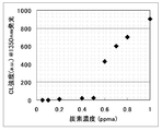
- FIG. 2 is a graph showing the relationship between the maximum intensity of the broad emission spectrum of CL and the carbon concentration of the substrate. As can be seen from FIG. 2, when the carbon concentration is 0.5 ppma or less, there is no CL emission, that is, defects formed by ion implantation are recovered.
- the following can be considered as the reason why the residual ion implantation defects decrease when the carbon concentration of the substrate decreases. That is, carbon has a relatively small atomic radius, and there is strain at the location where carbon is present, so interstitial silicon generated by ion implantation is likely to gather. Therefore, if the carbon concentration of the substrate is lowered, the number of regions where interstitial silicon is likely to collect decreases, so that the number of ion implantation defects remains.
- the following is considered as the reason why broad characteristic light emission is observed. That is, when flash lamp annealing is performed, the reaction in the middle of recovering ion implantation defects is quenched, and a complicated CL spectrum is shown.
- Example 1 As a sample, a polycrystalline raw material and a quartz crucible were used with high purity, and a single crystal silicon wafer cut from a p-type silicon single crystal having a diameter of 200 mm manufactured by doping only boron was used. This single crystal silicon wafer had a resistivity of 10 ⁇ ⁇ cm and a carbon concentration of 0.05 ppma. Boron is ion-implanted into this wafer at 10 keV at 5 ⁇ 10 13 atoms / cm 2 , and pre-heating at 500 ° C.
- the same substrate was prepared and oxidized to a thickness of 300 nm in a Pyro (water vapor) atmosphere at 1000 ° C., and this was subjected to photolithography to open a window in the oxide film.
- wet etching with hydrofluoric acid was used for oxide film etching after photolithography.
- boron is ion-implanted at 10 keV with 5 ⁇ 10 13 atoms / cm 2
- phosphorus is then ion-implanted with 3 keV at 5 ⁇ 10 14 atoms / cm 2 , followed by preheating at 500 ° C.
- Flash lamp annealing using a xenon lamp as a light source was performed under conditions of an irradiation energy of 22 J / cm 2 , an irradiation time of 1.4 milliseconds, and an irradiation temperature of 1200 ° C. to form a pn junction.
- the area of each pn junction was 4 mm 2 .
- the reverse leakage current value measured at the pn junction was 15 pA.
- Example 2 A single crystal silicon wafer cut out from a silicon single crystal produced by doping boron and a small amount of carbon was used as a sample.
- the carbon concentration of the single crystal silicon wafer at this time was 0.5 ppma.
- Boron is ion-implanted into this wafer at 10 keV at 5 ⁇ 10 13 atoms / cm 2 , and pre-heating at 500 ° C. is performed with flash lamp annealing using a xenon lamp as a light source with an irradiation energy of 22 J / cm 2 and an irradiation time of 1.4 milliseconds.
- the irradiation temperature was 1200 ° C.
- the same substrate was prepared, and a pn junction was formed in the same manner as in Example 1.
- the area of each pn junction was 4 mm 2 .
- the reverse leakage current value measured at the pn junction was 15 pA.
- Example 1 A single crystal silicon wafer cut out from a silicon single crystal produced by doping boron and a small amount of carbon as in Example 2 was used as a sample. However, the carbon concentration of the single crystal silicon wafer at this time was 1 ppma. Boron is ion-implanted into this wafer at 10 keV at 5 ⁇ 10 13 atoms / cm 2 , and pre-heating at 500 ° C. is performed with flash lamp annealing using a xenon lamp as a light source with an irradiation energy of 22 J / cm 2 and an irradiation time of 1.4 milliseconds. The irradiation temperature was 1200 ° C. Thereafter, when ion implantation defects were evaluated by CL, broad characteristic light emission was observed as shown in FIG.
- the same substrate was prepared, and a pn junction was formed in the same manner as in Example 1.
- the area of each pn junction was 4 mm 2 .
- the reverse leakage current value measured at the pn junction was 200 pA.
- Example 1-2 where the carbon concentration is 0.5 ppma or less, light emission other than the TO line due to silicon band edge light emission is not observed in the ion implantation defect evaluation by CL, and the leakage of the pn junction portion Although the current is small, at the level of Comparative Example 1 where the carbon concentration is 1 ppma, broad characteristic light emission is observed in the ion implantation defect evaluation by CL, and the leakage current of the pn junction is large. I understand.
- the present invention is not limited to the above embodiment.
- the above-described embodiment is an exemplification, and the present invention has substantially the same configuration as the technical idea described in the claims of the present invention, and any device that exhibits the same function and effect is the present invention. It is included in the technical scope of the invention.
Landscapes
- Insulated Gate Type Field-Effect Transistor (AREA)
- Crystals, And After-Treatments Of Crystals (AREA)
Abstract
Description
以上に述べた拡散による広がりを考慮しても、深さが15nm以下で、イオン注入用マスク直下横方向の広がりが10nm以下の浅い接合を形成できるようにするために、非常に短時間で高エネルギーを照射するアニール方法が検討され、採用されている(例えば、特許文献1-2参照)。
例えば、特許文献3には、半導体基板中にダメージを招かずに、浅い不純物拡散領域を形成するために、半導体基板に対してアクセプタまたはドナーとなる物質と、半導体基板に対してアクセプタまたはドナーにならない物質とを有する物質を半導体基板に注入することが記載されている。
このようなシリコンからなるフラッシュランプアニール用半導体基板に、本発明を好適に適用することができる。
このようなシリコンからなるアニール基板に、本発明を好適に適用することができる。
このアニール方法としては、キセノン等の希ガスを封入したフラッシュランプを使用したアニール等が挙げられるが、フラッシュランプアニールはこれに限定されず、非常に短時間で高エネルギーを照射するものであればよい。
このアニール方法は、高エネルギーを用いるがゆえに、シリコン基板中の熱応力が大きくなり、シリコン基板の割れやスリップといったダメージが生じることが考えられ、実際にこれに対する検討がされている。
しかしながら、イオン注入欠陥の残留を防止するという観点においては、改善の余地があった。
本発明者らは、シリコン基板の割れやスリップという観点ではなく、点欠陥挙動に着目し、炭素濃度が0.5ppma以下の半導体基板であれば、イオン注入を行い半導体基板表面にp-n接合を形成し、フラッシュランプアニールによりイオン注入欠陥を回復させる製造工程を用いた場合に、イオン注入欠陥の残留を簡単かつ確実に防止できることを見出し、本発明をなすに至った。
本発明のフラッシュランプアニール用半導体基板は、イオン注入を行い半導体基板表面にp-n接合を形成し、フラッシュランプアニールによりイオン注入欠陥を回復させる製造工程で用いられるものであり、半導体基板の炭素濃度が0.5ppma以下になっている。
このように、炭素濃度が0.5ppma以下の半導体基板であれば、イオン注入を行い半導体基板表面にp-n接合を形成し、フラッシュランプアニールによりイオン注入欠陥を回復させる製造工程に用いた場合に、イオン注入欠陥の残留を簡単かつ確実に防止できる。
このようなシリコンからなるフラッシュランプアニール用半導体基板に、本発明を好適に適用することができる。
本発明のアニール基板は、イオン注入を行い半導体基板表面にp-n接合を形成し、フラッシュランプアニールによりイオン注入欠陥を回復させたものであり、基板表面にp-n接合を有し、炭素濃度が0.5ppma以下になっているものである。
このように、炭素濃度が0.5ppma以下のアニール基板であれば、半導体基板表面におけるp-n接合形成時のイオン注入欠陥の残留を簡単かつ確実に防止できる。
このようなシリコンからなるアニール基板に、本発明を好適に適用することができる。
本発明の半導体装置は、上記のフラッシュランプアニール用半導体基板、又は、上記のアニール基板を用いて作製された半導体装置である。
本発明のフラッシュランプアニール用半導体基板、又は、本発明のアニール基板を用いて作製された半導体装置であれば、半導体基板表面におけるp-n接合形成時のイオン注入欠陥の残留を確実に防止でき、高い歩留まりを得ることができる高性能なものとすることができる。
本発明の半導体装置の製造方法は、半導体基板表面にp-n接合を形成する工程であって、イオン注入を行い、その後フラッシュランプアニールを行い、イオン注入欠陥を回復させる工程を含み、上記のアニールを、炭素濃度が0.5ppma以下の半導体基板を用いて行っている。
イオン注入後のフラッシュランプアニールを、炭素濃度が0.5ppma以下の半導体基板を用いて行うことで、半導体基板表面におけるp-n接合形成時のイオン注入欠陥の残留を簡単かつ確実に防止できる。
炭素濃度の低い単結晶シリコンウェーハ(炭素濃度:0.05ppma)と、炭素濃度の高い単結晶シリコンウェーハ(炭素濃度:1ppma)を準備し、これらにボロンをイオン注入した。このイオン注入により点欠陥がシリコン基板中に形成された。
その後、イオン注入による欠陥の回復と活性化のためにフラッシュランプアニールを行い、イオン注入による欠陥の回復状況を調査した。
TEM観察による評価と、CLを用いた評価との検出感度の違いは、以下の理由によるものと考えられる。すなわち、TEMは観察領域が狭い上に、点欠陥を像として捉えることが難しい一方で、CLは走査型電子顕微鏡(SEM)を用いているため観察領域(特に深さ方向)が大きく、また原理的に深い準位の発光中心を検出するため、検出感度が高い。
図2は、CLのブロードな発光スペクトルの最大強度と、基板の炭素濃度との関係を示す図である。
図2からわかるように、0.5ppma以下の炭素濃度であればCL発光がない、すなわち、イオン注入により形成された欠陥が回復している。
また、イオン注入欠陥が残留している場合に、ブロードな特徴ある発光が観測される理由として以下のことが考えられる。すなわち、フラッシュランプアニールを行った場合には、イオン注入欠陥を回復させる反応途中をクエンチしたような状況となり、複雑なCLスペクトルを示す。
試料として、多結晶原料及び石英ルツボは高純度のものを用い、ボロンのみをドープして製造したp型で直径200mmのシリコン単結晶から切り出した単結晶シリコンウェーハを用いた。この単結晶シリコンウェーハの抵抗率は10Ω・cm、炭素濃度は0.05ppmaであった。
このウェーハにボロンを10keVで5×10¹³atoms/cm2のイオン注入を行い、予備加熱500℃でキセノンランプを光源としたフラッシュランプアニールを照射エネルギー22J/cm2、照射時間1.4ミリ秒、照射温度1200℃の条件で施した。この後、CLにてイオン注入欠陥を評価したところ、図1に示すようにシリコンのバンド端発光に起因するTO線以外は観察されなかった。
この後、このウェーハにボロンを10keVで5×10¹³atoms/cm2のイオン注入を行い、次にリンを3keVで5×1014atoms/cm2のイオン注入を行い、その後予備加熱500℃でキセノンランプを光源としたフラッシュランプアニールを照射エネルギー22J/cm2、照射時間1.4ミリ秒、照射温度1200℃の条件で施しp-n接合を形成した。
p-n接合部の面積はそれぞれ4mm2とした。p-n接合部で測定した逆方向リーク電流値は15pAであった。
試料として、ボロンと微量の炭素をドープして製造したシリコン単結晶から切り出した単結晶シリコンウェーハを用いた。このときの単結晶シリコンウェーハの炭素濃度は0.5ppmaであった。
このウェーハにボロンを10keVで5×10¹³atoms/cm2のイオン注入を行い、予備加熱500℃でキセノンランプを光源としたフラッシュランプアニールを照射エネルギー22J/cm2、照射時間1.4ミリ秒、照射温度1200℃の条件で施した。この後、CLにてイオン注入欠陥を評価したところ、図1の炭素濃度が0.05ppmaの水準と同様に、シリコンのバンド端発光に起因するTO線以外は観察されなかった。
p-n接合部の面積はそれぞれ4mm2とした。p-n接合部で測定した逆方向リーク電流値は15pAであった。
試料として実施例2と同様にボロンと微量の炭素をドープして製造したシリコン単結晶から切り出した単結晶シリコンウェーハを用いた。ただし、このときの単結晶シリコンウェーハの炭素濃度は1ppmaであった。
このウェーハにボロンを10keVで5×10¹³atoms/cm2のイオン注入を行い、予備加熱500℃でキセノンランプを光源としたフラッシュランプアニールを照射エネルギー22J/cm2、照射時間1.4ミリ秒、照射温度1200℃の条件で施した。この後、CLにてイオン注入欠陥を評価したところ、図1に示すように、ブロードな特徴ある発光が観察された。
p-n接合部の面積はそれぞれ4mm2とした。p-n接合部で測定した逆方向リーク電流値は200pAであった。
Claims (7)
- イオン注入を行い半導体基板表面にp-n接合を形成し、フラッシュランプアニールによりイオン注入欠陥を回復させる製造工程で用いられるフラッシュランプアニール用半導体基板であって、前記半導体基板の炭素濃度が0.5ppma以下であることを特徴とするフラッシュランプアニール用半導体基板。
- 前記半導体基板がシリコンからなることを特徴とする請求項1に記載のフラッシュランプアニール用半導体基板。
- 請求項1又は請求項2に記載のフラッシュランプアニール用半導体基板を用いて作製されたものであることを特徴とする半導体装置。
- イオン注入を行い半導体基板表面にp-n接合を形成し、フラッシュランプアニールによりイオン注入欠陥を回復させたアニール基板であって、
前記アニール基板は、基板表面に前記p-n接合を有し、炭素濃度が0.5ppma以下であることを特徴とするアニール基板。 - 前記アニール基板がシリコンからなることを特徴とする請求項4に記載のアニール基板。
- 請求項4又は請求項5に記載のアニール基板を用いて作製されたものであることを特徴とする半導体装置。
- 半導体基板表面にp-n接合を形成する工程であって、イオン注入を行い、その後フラッシュランプアニールを行い、イオン注入欠陥を回復させる工程を含み、
前記アニールを、炭素濃度が0.5ppma以下の半導体基板を用いて行うことを特徴とする半導体装置の製造方法。
Priority Applications (4)
| Application Number | Priority Date | Filing Date | Title |
|---|---|---|---|
| DE112015000650.8T DE112015000650T5 (de) | 2014-02-26 | 2015-01-26 | Halbleitersubstrat für eine Blitzlampentemperung, Tempersubstrat, Halbleiterbauelement und Verfahren zum Herstellen eines Halbleiterbauelements |
| US15/117,269 US20160351415A1 (en) | 2014-02-26 | 2015-01-26 | Semiconductor substrate for flash lamp anneal, anneal substrate, semiconductor device, and method for manufacturing semiconductor device |
| KR1020167022696A KR20160125379A (ko) | 2014-02-26 | 2015-01-26 | 플래쉬 램프 어닐용 반도체기판, 어닐기판, 반도체장치, 그리고 반도체장치의 제조방법 |
| CN201580010104.3A CN106030762A (zh) | 2014-02-26 | 2015-01-26 | 闪光灯退火用半导体基板、退火基板、半导体装置、以及半导体装置的制造方法 |
Applications Claiming Priority (2)
| Application Number | Priority Date | Filing Date | Title |
|---|---|---|---|
| JP2014035156A JP6119637B2 (ja) | 2014-02-26 | 2014-02-26 | アニール基板の製造方法、及び半導体装置の製造方法 |
| JP2014-035156 | 2014-02-26 |
Publications (1)
| Publication Number | Publication Date |
|---|---|
| WO2015129155A1 true WO2015129155A1 (ja) | 2015-09-03 |
Family
ID=54008494
Family Applications (1)
| Application Number | Title | Priority Date | Filing Date |
|---|---|---|---|
| PCT/JP2015/000319 Ceased WO2015129155A1 (ja) | 2014-02-26 | 2015-01-26 | フラッシュランプアニール用半導体基板、アニール基板、半導体装置、並びに半導体装置の製造方法 |
Country Status (7)
| Country | Link |
|---|---|
| US (1) | US20160351415A1 (ja) |
| JP (1) | JP6119637B2 (ja) |
| KR (1) | KR20160125379A (ja) |
| CN (1) | CN106030762A (ja) |
| DE (1) | DE112015000650T5 (ja) |
| TW (1) | TWI596662B (ja) |
| WO (1) | WO2015129155A1 (ja) |
Families Citing this family (3)
| Publication number | Priority date | Publication date | Assignee | Title |
|---|---|---|---|---|
| JP6531729B2 (ja) * | 2016-07-19 | 2019-06-19 | 株式会社Sumco | シリコン試料の炭素濃度評価方法、シリコンウェーハ製造工程の評価方法、シリコンウェーハの製造方法およびシリコン単結晶インゴットの製造方法 |
| JP6852703B2 (ja) * | 2018-03-16 | 2021-03-31 | 信越半導体株式会社 | 炭素濃度評価方法 |
| JP2020155447A (ja) * | 2019-03-18 | 2020-09-24 | 信越半導体株式会社 | 半導体デバイスの形成方法 |
Citations (4)
| Publication number | Priority date | Publication date | Assignee | Title |
|---|---|---|---|---|
| JPH03184345A (ja) * | 1989-12-13 | 1991-08-12 | Nippon Steel Corp | シリコンウェハおよびその製造方法 |
| JPH05339093A (ja) * | 1992-06-10 | 1993-12-21 | Fujitsu Ltd | 低炭素シリコン結晶成長方法 |
| JP2002198322A (ja) * | 2000-12-27 | 2002-07-12 | Ushio Inc | 熱処理方法及びその装置 |
| JP2005347704A (ja) * | 2004-06-07 | 2005-12-15 | Toshiba Corp | 熱処理装置、熱処理方法及び半導体装置の製造方法 |
Family Cites Families (5)
| Publication number | Priority date | Publication date | Assignee | Title |
|---|---|---|---|---|
| US5147808A (en) * | 1988-11-02 | 1992-09-15 | Universal Energy Systems, Inc. | High energy ion implanted silicon on insulator structure |
| JP2002293691A (ja) * | 2001-03-30 | 2002-10-09 | Shin Etsu Handotai Co Ltd | シリコン単結晶の製造方法及びシリコン単結晶並びにシリコンウエーハ |
| JP2010147248A (ja) * | 2008-12-18 | 2010-07-01 | Siltronic Ag | アニールウェハおよびアニールウェハの製造方法 |
| TWI566300B (zh) * | 2011-03-23 | 2017-01-11 | 斯克林集團公司 | 熱處理方法及熱處理裝置 |
| JP5799936B2 (ja) * | 2012-11-13 | 2015-10-28 | 株式会社Sumco | 半導体エピタキシャルウェーハの製造方法、半導体エピタキシャルウェーハ、および固体撮像素子の製造方法 |
-
2014
- 2014-02-26 JP JP2014035156A patent/JP6119637B2/ja active Active
-
2015
- 2015-01-26 KR KR1020167022696A patent/KR20160125379A/ko not_active Withdrawn
- 2015-01-26 CN CN201580010104.3A patent/CN106030762A/zh active Pending
- 2015-01-26 WO PCT/JP2015/000319 patent/WO2015129155A1/ja not_active Ceased
- 2015-01-26 US US15/117,269 patent/US20160351415A1/en not_active Abandoned
- 2015-01-26 DE DE112015000650.8T patent/DE112015000650T5/de not_active Withdrawn
- 2015-02-10 TW TW104104377A patent/TWI596662B/zh active
Patent Citations (4)
| Publication number | Priority date | Publication date | Assignee | Title |
|---|---|---|---|---|
| JPH03184345A (ja) * | 1989-12-13 | 1991-08-12 | Nippon Steel Corp | シリコンウェハおよびその製造方法 |
| JPH05339093A (ja) * | 1992-06-10 | 1993-12-21 | Fujitsu Ltd | 低炭素シリコン結晶成長方法 |
| JP2002198322A (ja) * | 2000-12-27 | 2002-07-12 | Ushio Inc | 熱処理方法及びその装置 |
| JP2005347704A (ja) * | 2004-06-07 | 2005-12-15 | Toshiba Corp | 熱処理装置、熱処理方法及び半導体装置の製造方法 |
Also Published As
| Publication number | Publication date |
|---|---|
| TW201545212A (zh) | 2015-12-01 |
| CN106030762A (zh) | 2016-10-12 |
| JP2015162489A (ja) | 2015-09-07 |
| US20160351415A1 (en) | 2016-12-01 |
| KR20160125379A (ko) | 2016-10-31 |
| JP6119637B2 (ja) | 2017-04-26 |
| DE112015000650T5 (de) | 2016-10-27 |
| TWI596662B (zh) | 2017-08-21 |
Similar Documents
| Publication | Publication Date | Title |
|---|---|---|
| USRE49657E1 (en) | Epitaxial wafer manufacturing method and epitaxial wafer | |
| JP6083404B2 (ja) | 半導体基板の評価方法 | |
| JP6119637B2 (ja) | アニール基板の製造方法、及び半導体装置の製造方法 | |
| JP5200412B2 (ja) | Soi基板の製造方法 | |
| US20140273328A1 (en) | Semiconductor element producing method | |
| CN111902911A (zh) | 半导体外延晶片的制造方法以及半导体器件的制造方法 | |
| TW201923842A (zh) | 基板的熱處理方法 | |
| JP6323383B2 (ja) | 半導体装置の評価方法 | |
| TW201908543A (zh) | 半導體磊晶晶圓及其製造方法以及固體攝影元件的製造方法 | |
| JP5239460B2 (ja) | 半導体デバイス用シリコン単結晶ウェーハ及びその作製法 | |
| CN109891553B (zh) | 装置形成方法 | |
| JP6413938B2 (ja) | 半導体基板の評価方法 | |
| US11175231B2 (en) | Method for evaluating carbon concentration | |
| CN106653781A (zh) | 半导体器件的制造方法 | |
| JP2017044570A (ja) | 半導体評価方法 | |
| JP2015185811A (ja) | 半導体基板の評価方法 |
Legal Events
| Date | Code | Title | Description |
|---|---|---|---|
| 121 | Ep: the epo has been informed by wipo that ep was designated in this application |
Ref document number: 15756016 Country of ref document: EP Kind code of ref document: A1 |
|
| WWE | Wipo information: entry into national phase |
Ref document number: 15117269 Country of ref document: US |
|
| ENP | Entry into the national phase |
Ref document number: 20167022696 Country of ref document: KR Kind code of ref document: A |
|
| WWE | Wipo information: entry into national phase |
Ref document number: 112015000650 Country of ref document: DE |
|
| 122 | Ep: pct application non-entry in european phase |
Ref document number: 15756016 Country of ref document: EP Kind code of ref document: A1 |