WO2016006573A1 - Unité de circuit de génération de puissance - Google Patents
Unité de circuit de génération de puissance Download PDFInfo
- Publication number
- WO2016006573A1 WO2016006573A1 PCT/JP2015/069411 JP2015069411W WO2016006573A1 WO 2016006573 A1 WO2016006573 A1 WO 2016006573A1 JP 2015069411 W JP2015069411 W JP 2015069411W WO 2016006573 A1 WO2016006573 A1 WO 2016006573A1
- Authority
- WO
- WIPO (PCT)
- Prior art keywords
- substrate
- power generation
- piece
- state
- connecting portion
- Prior art date
- Legal status (The legal status is an assumption and is not a legal conclusion. Google has not performed a legal analysis and makes no representation as to the accuracy of the status listed.)
- Ceased
Links
Images







Classifications
-
- H—ELECTRICITY
- H10—SEMICONDUCTOR DEVICES; ELECTRIC SOLID-STATE DEVICES NOT OTHERWISE PROVIDED FOR
- H10F—INORGANIC SEMICONDUCTOR DEVICES SENSITIVE TO INFRARED RADIATION, LIGHT, ELECTROMAGNETIC RADIATION OF SHORTER WAVELENGTH OR CORPUSCULAR RADIATION
- H10F77/00—Constructional details of devices covered by this subclass
- H10F77/10—Semiconductor bodies
- H10F77/16—Material structures, e.g. crystalline structures, film structures or crystal plane orientations
- H10F77/169—Thin semiconductor films on metallic or insulating substrates
- H10F77/1698—Thin semiconductor films on metallic or insulating substrates the metallic or insulating substrates being flexible
-
- H—ELECTRICITY
- H02—GENERATION; CONVERSION OR DISTRIBUTION OF ELECTRIC POWER
- H02S—GENERATION OF ELECTRIC POWER BY CONVERSION OF INFRARED RADIATION, VISIBLE LIGHT OR ULTRAVIOLET LIGHT, e.g. USING PHOTOVOLTAIC [PV] MODULES
- H02S20/00—Supporting structures for PV modules
- H02S20/30—Supporting structures being movable or adjustable, e.g. for angle adjustment
- H02S20/32—Supporting structures being movable or adjustable, e.g. for angle adjustment specially adapted for solar tracking
-
- H—ELECTRICITY
- H02—GENERATION; CONVERSION OR DISTRIBUTION OF ELECTRIC POWER
- H02S—GENERATION OF ELECTRIC POWER BY CONVERSION OF INFRARED RADIATION, VISIBLE LIGHT OR ULTRAVIOLET LIGHT, e.g. USING PHOTOVOLTAIC [PV] MODULES
- H02S30/00—Structural details of PV modules other than those related to light conversion
- H02S30/10—Frame structures
-
- H—ELECTRICITY
- H02—GENERATION; CONVERSION OR DISTRIBUTION OF ELECTRIC POWER
- H02S—GENERATION OF ELECTRIC POWER BY CONVERSION OF INFRARED RADIATION, VISIBLE LIGHT OR ULTRAVIOLET LIGHT, e.g. USING PHOTOVOLTAIC [PV] MODULES
- H02S40/00—Components or accessories in combination with PV modules, not provided for in groups H02S10/00 - H02S30/00
- H02S40/20—Optical components
- H02S40/22—Light-reflecting or light-concentrating means
-
- H—ELECTRICITY
- H02—GENERATION; CONVERSION OR DISTRIBUTION OF ELECTRIC POWER
- H02S—GENERATION OF ELECTRIC POWER BY CONVERSION OF INFRARED RADIATION, VISIBLE LIGHT OR ULTRAVIOLET LIGHT, e.g. USING PHOTOVOLTAIC [PV] MODULES
- H02S40/00—Components or accessories in combination with PV modules, not provided for in groups H02S10/00 - H02S30/00
- H02S40/40—Thermal components
- H02S40/42—Cooling means
-
- H—ELECTRICITY
- H05—ELECTRIC TECHNIQUES NOT OTHERWISE PROVIDED FOR
- H05K—PRINTED CIRCUITS; CASINGS OR CONSTRUCTIONAL DETAILS OF ELECTRIC APPARATUS; MANUFACTURE OF ASSEMBLAGES OF ELECTRICAL COMPONENTS
- H05K1/00—Printed circuits
- H05K1/02—Details
- H05K1/0277—Bendability or stretchability details
- H05K1/028—Bending or folding regions of flexible printed circuits
-
- H—ELECTRICITY
- H05—ELECTRIC TECHNIQUES NOT OTHERWISE PROVIDED FOR
- H05K—PRINTED CIRCUITS; CASINGS OR CONSTRUCTIONAL DETAILS OF ELECTRIC APPARATUS; MANUFACTURE OF ASSEMBLAGES OF ELECTRICAL COMPONENTS
- H05K1/00—Printed circuits
- H05K1/18—Printed circuits structurally associated with non-printed electric components
- H05K1/189—Printed circuits structurally associated with non-printed electric components characterised by the use of flexible or folded printed circuits
-
- H—ELECTRICITY
- H10—SEMICONDUCTOR DEVICES; ELECTRIC SOLID-STATE DEVICES NOT OTHERWISE PROVIDED FOR
- H10F—INORGANIC SEMICONDUCTOR DEVICES SENSITIVE TO INFRARED RADIATION, LIGHT, ELECTROMAGNETIC RADIATION OF SHORTER WAVELENGTH OR CORPUSCULAR RADIATION
- H10F10/00—Individual photovoltaic cells, e.g. solar cells
-
- H—ELECTRICITY
- H10—SEMICONDUCTOR DEVICES; ELECTRIC SOLID-STATE DEVICES NOT OTHERWISE PROVIDED FOR
- H10F—INORGANIC SEMICONDUCTOR DEVICES SENSITIVE TO INFRARED RADIATION, LIGHT, ELECTROMAGNETIC RADIATION OF SHORTER WAVELENGTH OR CORPUSCULAR RADIATION
- H10F19/00—Integrated devices, or assemblies of multiple devices, comprising at least one photovoltaic cell covered by group H10F10/00, e.g. photovoltaic modules
- H10F19/90—Structures for connecting between photovoltaic cells, e.g. interconnections or insulating spacers
- H10F19/902—Structures for connecting between photovoltaic cells, e.g. interconnections or insulating spacers for series or parallel connection of photovoltaic cells
- H10F19/904—Structures for connecting between photovoltaic cells, e.g. interconnections or insulating spacers for series or parallel connection of photovoltaic cells characterised by the shapes of the structures
-
- H—ELECTRICITY
- H10—SEMICONDUCTOR DEVICES; ELECTRIC SOLID-STATE DEVICES NOT OTHERWISE PROVIDED FOR
- H10F—INORGANIC SEMICONDUCTOR DEVICES SENSITIVE TO INFRARED RADIATION, LIGHT, ELECTROMAGNETIC RADIATION OF SHORTER WAVELENGTH OR CORPUSCULAR RADIATION
- H10F77/00—Constructional details of devices covered by this subclass
- H10F77/40—Optical elements or arrangements
- H10F77/42—Optical elements or arrangements directly associated or integrated with photovoltaic cells, e.g. light-reflecting means or light-concentrating means
- H10F77/484—Refractive light-concentrating means, e.g. lenses
-
- H—ELECTRICITY
- H10—SEMICONDUCTOR DEVICES; ELECTRIC SOLID-STATE DEVICES NOT OTHERWISE PROVIDED FOR
- H10F—INORGANIC SEMICONDUCTOR DEVICES SENSITIVE TO INFRARED RADIATION, LIGHT, ELECTROMAGNETIC RADIATION OF SHORTER WAVELENGTH OR CORPUSCULAR RADIATION
- H10F77/00—Constructional details of devices covered by this subclass
- H10F77/93—Interconnections
- H10F77/933—Interconnections for devices having potential barriers
- H10F77/935—Interconnections for devices having potential barriers for photovoltaic devices or modules
- H10F77/939—Output lead wires or elements
-
- H—ELECTRICITY
- H05—ELECTRIC TECHNIQUES NOT OTHERWISE PROVIDED FOR
- H05K—PRINTED CIRCUITS; CASINGS OR CONSTRUCTIONAL DETAILS OF ELECTRIC APPARATUS; MANUFACTURE OF ASSEMBLAGES OF ELECTRICAL COMPONENTS
- H05K1/00—Printed circuits
-
- H—ELECTRICITY
- H05—ELECTRIC TECHNIQUES NOT OTHERWISE PROVIDED FOR
- H05K—PRINTED CIRCUITS; CASINGS OR CONSTRUCTIONAL DETAILS OF ELECTRIC APPARATUS; MANUFACTURE OF ASSEMBLAGES OF ELECTRICAL COMPONENTS
- H05K2201/00—Indexing scheme relating to printed circuits covered by H05K1/00
- H05K2201/04—Assemblies of printed circuits
- H05K2201/046—Planar parts of folded PCBs making an angle relative to each other
-
- H—ELECTRICITY
- H05—ELECTRIC TECHNIQUES NOT OTHERWISE PROVIDED FOR
- H05K—PRINTED CIRCUITS; CASINGS OR CONSTRUCTIONAL DETAILS OF ELECTRIC APPARATUS; MANUFACTURE OF ASSEMBLAGES OF ELECTRICAL COMPONENTS
- H05K2201/00—Indexing scheme relating to printed circuits covered by H05K1/00
- H05K2201/05—Flexible printed circuits [FPCs]
-
- H—ELECTRICITY
- H05—ELECTRIC TECHNIQUES NOT OTHERWISE PROVIDED FOR
- H05K—PRINTED CIRCUITS; CASINGS OR CONSTRUCTIONAL DETAILS OF ELECTRIC APPARATUS; MANUFACTURE OF ASSEMBLAGES OF ELECTRICAL COMPONENTS
- H05K2201/00—Indexing scheme relating to printed circuits covered by H05K1/00
- H05K2201/09—Shape and layout
- H05K2201/09209—Shape and layout details of conductors
- H05K2201/09218—Conductive traces
- H05K2201/09263—Meander
-
- H—ELECTRICITY
- H05—ELECTRIC TECHNIQUES NOT OTHERWISE PROVIDED FOR
- H05K—PRINTED CIRCUITS; CASINGS OR CONSTRUCTIONAL DETAILS OF ELECTRIC APPARATUS; MANUFACTURE OF ASSEMBLAGES OF ELECTRICAL COMPONENTS
- H05K2201/00—Indexing scheme relating to printed circuits covered by H05K1/00
- H05K2201/10—Details of components or other objects attached to or integrated in a printed circuit board
- H05K2201/10007—Types of components
- H05K2201/10121—Optical component, e.g. opto-electronic component
-
- H—ELECTRICITY
- H05—ELECTRIC TECHNIQUES NOT OTHERWISE PROVIDED FOR
- H05K—PRINTED CIRCUITS; CASINGS OR CONSTRUCTIONAL DETAILS OF ELECTRIC APPARATUS; MANUFACTURE OF ASSEMBLAGES OF ELECTRICAL COMPONENTS
- H05K2201/00—Indexing scheme relating to printed circuits covered by H05K1/00
- H05K2201/20—Details of printed circuits not provided for in H05K2201/01 - H05K2201/10
-
- H—ELECTRICITY
- H05—ELECTRIC TECHNIQUES NOT OTHERWISE PROVIDED FOR
- H05K—PRINTED CIRCUITS; CASINGS OR CONSTRUCTIONAL DETAILS OF ELECTRIC APPARATUS; MANUFACTURE OF ASSEMBLAGES OF ELECTRICAL COMPONENTS
- H05K3/00—Apparatus or processes for manufacturing printed circuits
-
- H—ELECTRICITY
- H05—ELECTRIC TECHNIQUES NOT OTHERWISE PROVIDED FOR
- H05K—PRINTED CIRCUITS; CASINGS OR CONSTRUCTIONAL DETAILS OF ELECTRIC APPARATUS; MANUFACTURE OF ASSEMBLAGES OF ELECTRICAL COMPONENTS
- H05K3/00—Apparatus or processes for manufacturing printed circuits
- H05K3/36—Assembling printed circuits with other printed circuits
-
- H—ELECTRICITY
- H05—ELECTRIC TECHNIQUES NOT OTHERWISE PROVIDED FOR
- H05K—PRINTED CIRCUITS; CASINGS OR CONSTRUCTIONAL DETAILS OF ELECTRIC APPARATUS; MANUFACTURE OF ASSEMBLAGES OF ELECTRICAL COMPONENTS
- H05K3/00—Apparatus or processes for manufacturing printed circuits
- H05K3/40—Forming printed elements for providing electric connections to or between printed circuits
-
- Y—GENERAL TAGGING OF NEW TECHNOLOGICAL DEVELOPMENTS; GENERAL TAGGING OF CROSS-SECTIONAL TECHNOLOGIES SPANNING OVER SEVERAL SECTIONS OF THE IPC; TECHNICAL SUBJECTS COVERED BY FORMER USPC CROSS-REFERENCE ART COLLECTIONS [XRACs] AND DIGESTS
- Y02—TECHNOLOGIES OR APPLICATIONS FOR MITIGATION OR ADAPTATION AGAINST CLIMATE CHANGE
- Y02E—REDUCTION OF GREENHOUSE GAS [GHG] EMISSIONS, RELATED TO ENERGY GENERATION, TRANSMISSION OR DISTRIBUTION
- Y02E10/00—Energy generation through renewable energy sources
- Y02E10/50—Photovoltaic [PV] energy
-
- Y—GENERAL TAGGING OF NEW TECHNOLOGICAL DEVELOPMENTS; GENERAL TAGGING OF CROSS-SECTIONAL TECHNOLOGIES SPANNING OVER SEVERAL SECTIONS OF THE IPC; TECHNICAL SUBJECTS COVERED BY FORMER USPC CROSS-REFERENCE ART COLLECTIONS [XRACs] AND DIGESTS
- Y02—TECHNOLOGIES OR APPLICATIONS FOR MITIGATION OR ADAPTATION AGAINST CLIMATE CHANGE
- Y02E—REDUCTION OF GREENHOUSE GAS [GHG] EMISSIONS, RELATED TO ENERGY GENERATION, TRANSMISSION OR DISTRIBUTION
- Y02E10/00—Energy generation through renewable energy sources
- Y02E10/50—Photovoltaic [PV] energy
- Y02E10/52—PV systems with concentrators
Definitions
- the present invention relates to a power generation circuit unit, and particularly relates to a power generation circuit unit including FPC (Flexible Printed Circuits).
- FPC Flexible Printed Circuits
- Patent Document 1 discloses the following technology. That is, the concentrating solar cell module includes a plurality of solar cell elements, a long receiver substrate in which the solar cell elements are placed in a row at a predetermined interval, and the receiver substrate. A plurality of module boards placed in parallel at a certain interval, and the receiver board has a long receiver base and a longitudinal direction with its ends facing each other on the receiver base.
- a plurality of wiring members arranged in a row along a line, wherein a positive electrode pad portion is provided at one end portion of the wiring material, and a negative electrode pad portion is provided at the other end portion, and the positive electrode A positive electrode terminal and a negative electrode terminal of the solar cell element are connected to the pad portion and the negative electrode pad portion, respectively, to constitute a solar cell element mounting portion.
- the solar cell element when sunlight is converged on the solar cell element by the lens, the solar cell element becomes high temperature. When the heat of the solar cell element is transferred to the receiver substrate on which the solar cell element is mounted, the receiver substrate is thermally expanded.
- the receiver board that has been thermally expanded by sunlight during the day shrinks to its original size after, for example, the evening.
- the receiver substrate may be deteriorated earlier.
- the present invention has been made to solve the above-described problems, and an object of the present invention is to provide a power generation circuit unit capable of suppressing a temperature rise of a substrate on which a power generation element is mounted.
- a power generation circuit unit includes a wiring board and a plurality of power generation elements mounted on the wiring board, and the wiring board includes a first board on which the power generation elements are mounted. And a second substrate, and a connecting portion that connects the first substrate and the second substrate, wherein the first substrate is separated from the second substrate by a first distance, and the second substrate.
- the connecting portion includes FPC (Flexible Printed Circuits), and the first substrate is the second position. In the state of being disposed at a position, at least a part of the connecting portion is twisted.
- the temperature rise of the substrate on which the power generation element is mounted can be suppressed.
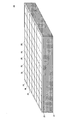
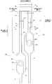
- FIG. 1 is a perspective view of a photovoltaic power generation apparatus according to an embodiment of the present invention.
- FIG. 2 is a perspective view of the photovoltaic power generation module according to the embodiment of the present invention.
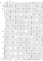
- FIG. 3 is a plan view of the photovoltaic power generation module according to the embodiment of the present invention.
- FIG. 4 is a plan view showing a state in which the light collecting unit is removed from the photovoltaic power generation module according to the embodiment of the present invention.
- FIG. 1 is a perspective view of a photovoltaic power generation apparatus according to an embodiment of the present invention.
- FIG. 2 is a perspective view of the photovoltaic power generation module according to the embodiment of the present invention.
- FIG. 7 is a cross-sectional view showing a cross section taken along line VII-VII in FIG. 4 of the photovoltaic power generation module according to the embodiment of the present invention.
- FIG. 8 is a diagram showing a pattern of the conductive portion of the FPC in the wiring board according to the embodiment of the present invention.
- FIG. 9 is a diagram showing a state in which the connecting portion is not twisted in the wiring board according to the embodiment of the present invention.
- FIG. 10 is a diagram showing in detail a state in which the connecting portion is not twisted in the wiring board according to the embodiment of the present invention.
- FIG. 11 is a diagram showing in detail a state in which the connecting portion is twisted in the wiring board according to the embodiment of the present invention.
- FIG. 12 is a perspective view showing a twisted state of the connecting portion in the wiring board according to the embodiment of the present invention.
- FIG. 13 is a perspective view showing a twisted state of the connecting portion in the wiring board according to the embodiment of the present invention.
- a power generation circuit unit includes a wiring board and a plurality of power generation elements mounted on the wiring board, and the wiring board includes a first on which the power generation elements are mounted.
- a first portion that is separated from the second substrate by a first distance; and a second position that includes a substrate and a second substrate, and a connecting portion that connects the first substrate and the second substrate.
- the connecting portion has FPC (Flexible Printed Circuits), and the first substrate is the first substrate. In the state of being arranged at two positions, at least a part of the connecting portion is twisted.
- the connecting portion can be easily twisted by changing the arrangement of the first substrate.
- air flowing around the wiring board is likely to hit the connecting portion, so that heat transferred from the power generating element to the wiring substrate is efficiently released from the connecting portion into the air. be able to. Therefore, the temperature rise of the substrate on which the power generation element is mounted can be suppressed.
- At least a part of the connecting portion is above a height position of at least one of the first substrate and the second substrate. Is located.
- Such a configuration makes it easier for a larger flow of air to hit the connecting portion, so that the heat dissipation efficiency of the connecting portion can be further increased.
- connection part includes a first connection piece, a second connection piece, and an intermediate piece, and the first connection piece connects the first substrate and the intermediate piece, The second connecting piece connects the second substrate and the intermediate piece.
- connection part can be twisted more easily by the structure in which the connection part is divided into a plurality of parts.
- At least one of the first connection piece, the second connection piece, and the intermediate piece is twisted in a state where the first substrate is disposed at the second position.
- both the first connection piece and the second connection piece are twisted in a state where the first substrate is disposed at the second position.
- the heat dissipation efficiency of the connecting portion can be further increased while twisting the connecting portion more easily.
- the first connecting piece is located above the height position of the first substrate.
- the intermediate piece is positioned above a height position above the first substrate.
- the length of the first connecting piece in the extending direction is different from the length of the second connecting piece in the extending direction.
- the extending direction of the intermediate piece is different from the extending direction of the first connecting piece.
- the extending direction of the intermediate piece is different from the extending direction of the second connecting piece.
- Such a configuration can more easily twist the connecting portion.
- the thickness direction of at least a part of the first connecting piece is different from the thickness direction of the first substrate.
- a thickness direction of at least a part of the second connecting piece is different from a thickness direction of the second substrate.
- Such a configuration makes it easier for air flowing around the wiring board to hit the connecting portion, so that the heat dissipation efficiency of the connecting portion can be further increased.
- the thickness direction of at least a part of the intermediate piece is the thickness of at least one of the first connection piece and the second connection piece. Different from direction.
- the distance between the first substrate and the intermediate piece is different from the distance between the second substrate and the intermediate piece in a state where the first substrate is disposed at the second position.
- the FPC is continuous over the first connection piece, the intermediate piece, and the second connection piece, and the FPC includes a conductive portion provided along the extending direction of the FPC; An insulating portion that covers the conductive portion, and at least one of the first connecting piece and the second connecting piece has a wide portion.
- FIG. 1 is a perspective view of a photovoltaic power generation apparatus according to an embodiment of the present invention.
- the solar power generation device 101 includes a solar power generation panel 12 and a gantry 40.
- the photovoltaic power generation panel 12 includes a plurality of photovoltaic power generation modules 10, a solar direction sensor 13, and a frame portion 14.
- the gantry 40 includes a base 46, a support column 48, a functional unit 90, and a position variable unit (not shown).
- the solar power generation panel 12 includes, for example, five rows and five columns of solar power generation modules 10, that is, 25 solar power generation modules 10. Each photovoltaic power generation module 10 is mounted side by side on top of the frame portion 14.
- the photovoltaic power generation module 10 receives sunlight to generate power, and outputs the generated DC power to the functional unit 90 attached to the side surface of the support column 48 using wiring (not shown).
- the support column 48 is erected perpendicularly to the ground, for example, on a base 46 provided on the ground.
- the position variable unit (not shown) includes a motor and, based on a control signal from the function unit 90, directs the direction of the light receiving surface FL in the photovoltaic power generation panel 12, that is, the normal direction of the light receiving surface FL indicated by the arrow As to the sun. During the period from sunrise to sunset, the direction of the light receiving surface FL operates so as to track the sun.
- the solar direction sensor 13 is used to detect the direction of the sun, and outputs a sensor signal indicating the detection result to the functional unit 90.
- the functional unit 90 includes, for example, a housing and various units housed in the housing. Specifically, for example, in the casing, a connection box for connecting wiring from each solar power generation module 10, a power conditioner that converts DC power output from the solar power generation module 10 into AC power, and A control unit and the like for controlling the direction of the light receiving surface FL in the photovoltaic power generation panel 12 are accommodated.
- FIG. 2 is a perspective view of the photovoltaic power generation module according to the embodiment of the present invention.
- FIG. 3 is a plan view of the photovoltaic power generation module according to the embodiment of the present invention.
- solar power generation module 10 includes a wall portion 27, a bottom portion (not shown), and a light collecting portion 25.
- the light collecting unit 25 includes a plurality of Fresnel lenses 26.
- the Fresnel lens 26 is arranged in a square lattice, for example. Specifically, the Fresnel lenses 26 are arranged such that, for example, the distance between the centers of adjacent Fresnel lenses 26 is the same W1.
- the size of the Fresnel lens 26 is, for example, 50 mm ⁇ 50 mm.
- FIG. 4 is a plan view showing a state in which the light collecting unit is removed from the photovoltaic power generation module according to the embodiment of the present invention.
- the solar power generation module 10 includes a wall portion 27, a base portion 38 that is a bottom portion of the solar power generation module 10, a power generation circuit unit 15, and two lead wires 39.
- the power generation circuit unit 15 includes a wiring board 69 and a plurality of power generation units 30 mounted on the wiring board 69.
- the power generation unit 30 includes a power generation element (not shown), and the power generation element is mounted on the wiring board 69.
- the wiring board 69 includes strip-like boards (first board or second board) 32A, 32B, 32C, 32D, 32E, 32F, 32G, 32H, 32I, and 32J, and connecting portions 33H, 33I, 33J, 33K, 33L, and 33M. , 33N, 33O, 33P.
- the connecting portion 33H connects the strip substrate 32A and the strip substrate 32B.
- the connecting portion 33I connects the strip substrate 32B and the strip substrate 32C.
- the connecting portion 33J connects the strip substrate 32C and the strip substrate 32D.
- the connecting portion 33K connects the strip substrate 32D and the strip substrate 32E.
- the connecting portion 33L connects the strip substrate 32E and the strip substrate 32F.
- the connecting portion 33M connects the strip substrate 32F and the strip substrate 32G.
- the connecting portion 33N connects the strip substrate 32G and the strip substrate 32H.
- the connecting portion 33O connects the strip substrate 32H and the strip substrate 32I.
- the connecting portion 33P connects the strip substrate 32I and the strip substrate 32J.
- each of the strip-shaped substrates 32A, 32B, 32C, 32D, 32E, 32F, 32G, 32H, 32I, and 32J is also referred to as a strip-shaped substrate 32.
- each of the connecting portions 33H, 33I, 33J, 33K, 33L, 33M, 33N, 33O, and 33P is also referred to as a connecting portion 33.
- Each strip substrate 32 is arranged in parallel to each other.
- each belt-like substrate 32 is arranged such that the distance from the adjacent belt-like substrate 32 is a distance G2.
- each connecting portion 33 is twisted. Details of the twisting of the connecting portion 33 will be described later with reference to FIGS.
- the wiring board 69 may be configured to further include a large number or a small number of strip-shaped substrates 32 and connecting portions 33.
- the wiring board 69 may be configured to include one connecting portion 33 and two strip-like substrates 32 connected by the connecting portion 33.
- a lead wire 39 is connected to each of the two ends of the wiring board 69.
- the lead wire 39 passes through a through hole provided in the base portion 38 and is connected to, for example, a connection box in the functional portion 90 shown in FIG.
- the material of the base portion 38 is, for example, aluminum or copper having high heat conductivity and relatively light weight.
- the wiring board 69 is placed on and adhered to the main surface on the upper side of the base portion 38, that is, the main surface on the Fresnel lens 26 side.
- the belt-like board 32 includes seven land parts 60 and wiring parts 63 connected to both sides of each land part.
- the wiring part 63 connects the land parts 60 to each other.
- the width of the land portion 60 is larger than the width of the wiring portion 63.
- the power generation unit 30 is mounted on the upper main surface of the land unit 60.
- the belt-like substrate 32 may further include a large number or a small number of land portions 60 and wiring portions 63.
- the belt-like substrate 32 may be configured to include one land portion 60 and two wiring portions 63.
- power generation units 30P1, 30Q1, and 30R1 are mounted as the power generation unit 30 on the belt-like substrate 32E.
- power generation units 30P2, 30Q2, and 30R2 are mounted on the belt-like substrate 32F as the power generation unit 30.
- the power generation units 30P1, 30Q1, and 30R1 mounted on the strip substrate 32E are opposed to the power generation units 30P2, 30Q2, and 30R2 mounted on the strip substrate 32F, respectively.
- the distance W2 between the power generation units 30 facing each other is equal to the distance W3 between the power generation units 30 adjacent to each other in the strip substrate 32.
- the distance W2 between the power generation unit 30P1 and the power generation unit 30P2 which are the power generation units 30 facing each other is equal to the distance W3 between the power generation unit 30P2 and the power generation unit 30Q2 adjacent to each other in the strip substrate 32F.
- the distance W2 and the distance W3 are equal to the distance W1 between the centers of the Fresnel lenses 26 shown in FIG.
- Fresnel lens 26 shown in FIG. 3 is provided for one power generation unit 30.
- Each power generation unit 30 is disposed on the optical axis of the corresponding Fresnel lens 26.
- FIG. 5 is a perspective view of a part of the power generation circuit unit according to the embodiment of the present invention.
- FIG. 5 shows a state in which the power generation unit 30 is mounted on the land portion 60 of the strip-shaped substrate 32 in the wiring substrate 69.
- wiring board 69 includes a power generation unit 30, an FPC (Flexible Printed Circuits) 79, and a reinforcing plate 89.
- the FPC 79 includes a conductive portion 77 and an insulating portion 78 that covers the conductive portion 77.
- the power generation unit 30 is mounted on the land portion 60 of the wiring board 69. Specifically, in the land portion 60, an opening 68 is provided in the FPC 79. In the opening 68, since the insulating part 78 does not cover the upper side of the conductive part 77, the conductive part 77 is exposed. The power generation unit 30 is electrically connected to the conductive unit 77 at the opening 68.
- the reinforcing plate 89 is provided on the main surface of the wiring board 69 on the base portion 38 side of the belt-like substrate 32, gives the belt-like substrate 32 a slight hardness, and the wiring board 69 at the time of manufacturing the photovoltaic power generation module 10. Easy handling.
- the reinforcing plate 89 is made of a metal such as aluminum or copper.
- the connecting portion 33 shown in FIG. 4 includes the FPC 79 and does not include the reinforcing plate 89.
- the FPC 79 in the belt-like substrate 32 and the FPC 79 in the connecting portion 33 are continuous. Since the connecting portion 33 does not include the reinforcing plate 89, the connecting portion 33 has higher flexibility than the belt-like substrate 32.
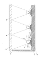
- FIG. 6 is a cross-sectional view showing a cross section taken along line VI-VI in FIG. 4 of the photovoltaic power generation module according to the embodiment of the present invention.
- the power generation unit 30 includes a ball lens 17, a package 18, and a power generation element 19. Note that the power generation unit 30 may have a configuration that does not include all or part of the components other than the power generation element 19.
- the wiring board 69 is placed on the upper main surface of the base portion 38.
- the reinforcing plate 89 is provided on the base portion 38.
- the FPC 79 is provided on the reinforcing plate 89. Specifically, the FPC 79 is provided on the base portion 38 via the reinforcing plate 89.
- the power generation element 19 is housed in the package 18.
- the power generating element 19 is mounted on the FPC 79 while being housed in the package 18.
- the electrode of the power generation element 19 (not shown) is connected to the conductive portion 77 of the FPC 79 via the package electrode 20 provided so as to penetrate the bottom of the package 18.
- the size of the power generation element 19 is, for example, 3.2 mm ⁇ 3.2 mm.
- the Fresnel lens 26 converges sunlight on the corresponding ball lens 17.
- the ball lens 17 further converges the sunlight converged by the Fresnel lens 26 onto the power generation element 19.
- the power generation element 19 receives sunlight converged by the Fresnel lens 26 and the ball lens 17 and generates electric power corresponding to the amount of received light.
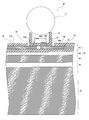
- FIG. 7 is a cross-sectional view showing a cross section taken along line VII-VII in FIG. 4 of the photovoltaic power generation module according to the embodiment of the present invention.
- FIG. 7 also shows an adhesive layer not shown in FIG. 5, for example. Specifically, referring to FIG. 7, in band-like substrate 32, FPC 79 and reinforcing plate 89 are bonded by an in-substrate adhesive layer 58.
- the strip substrate 32 is bonded to the base portion 38 by the base adhesive layer 59.
- the in-substrate adhesive layer 58 and the base adhesive layer 59 are formed by, for example, an adhesive or an adhesive tape.
- the connecting portion 33 shown in FIG. 4 is not bonded to the base portion 38.
- the power generation element 19 has an element electrode 42A and an element electrode 42B, and outputs a voltage from the element electrode 42A and the element electrode 42B.
- Package 18 includes package electrode 20A and package electrode 20B.
- the package electrode 20A and the package electrode 20B are provided so as to penetrate the bottom portion of the package 18, and are exposed on both the upper side and the lower side of the bottom portion.
- the element electrode 42A of the power generation element 19 is connected to the package electrode 20A by wire bonding, for example.
- the element electrode 42B is connected to the package electrode 20B by, for example, a conductive paste.
- the insulating portion 78 does not cover the upper side of the conductive portion 77, a part of the conductive portion 77, specifically, a portion of the conductive portion 77A and a portion of the conductive portion 77B are exposed. Yes.
- the package electrode 20A and the package electrode 20B are connected to the conductive portion 77A and the conductive portion 77B, for example, by soldering.
- the package 18 supports the ball lens 17 at the end of its side wall, and fixes the focal point of the ball lens 17 to the power generation element 19.
- FIG. 8 is a diagram showing a pattern of the conductive portion of the FPC in the wiring board according to the embodiment of the present invention.
- a part of the conductive portion 77 is exposed at the opening 68 of the FPC 79. Specifically, in the opening 68, a part of the conductive part 77A and the conductive part 77B are exposed.
- the conductive portion 77A and the conductive portion 77B are connected to the element electrode 42A and the element electrode 42B of the power generating element 19, respectively, for example, as shown in FIG.
- the conductive unit 77 connects, for example, the power generation unit 30 mounted on the land unit 60 and the power generation unit 30 mounted on the land unit 60 adjacent to the land unit 60 in series.
- FIG. 9 is a diagram showing a state in which the connecting portion is not twisted in the wiring board according to the embodiment of the present invention.
- the boundaries between the strip substrate 32 and the connecting portion 33 are defined as boundaries B11 to B28.
- the connecting portion 33 in the wiring board 69 is not twisted. That is, the wiring board 69 is planar.
- the connecting portion 33 is twisted as the distance between the two strip-like substrates 32 to be connected increases.
- FIG. 10 is a diagram showing in detail a state where the connecting portion is not twisted in the wiring board according to the embodiment of the present invention.
- FIG. 10 representatively shows the strip-shaped substrate 32E, the strip-shaped substrate 32F, and the connecting portion 33L.
- the connecting portion 33 ⁇ / b> L includes, for example, a first connecting piece 144, a second connecting piece 244, and an intermediate piece 344.
- the first connecting piece 144 connects the belt-like substrate 32E and the intermediate piece 344.
- the second connecting piece 244 connects the belt-like substrate 32F and the intermediate piece 344.
- the strip-shaped substrates 32E and 32F are separated by a distance G1.
- the belt-like substrate 32E is arranged with reference to the belt-like substrate 32F. This position is also referred to as a first position.
- the length L1 in the extending direction of the first connecting piece 144 is different from the length L2 in the extending direction of the second connecting piece 244, for example. Specifically, for example, the length L1 is larger than the length L2.
- the extending direction of the intermediate piece 344 is different from, for example, the extending direction of the first connecting piece 144.
- the extending direction of the intermediate piece 344 is different from the extending direction of the second connecting piece 244.
- the FPC 79 is continuous over the first connecting piece 144, the intermediate piece 344, and the second connecting piece 244.
- the FPC 79 includes, for example, a conductive portion 77 provided along the extending direction of the FPC 79 and an insulating portion 78 that covers the conductive portion 77 as described above.
- the insulating part 78 in the first connecting piece 144 has a wide part 145.
- the width W11 of the wide portion 145 is larger than the width W12 of a portion other than the wide portion 145.
- the wide portion 145 is formed such that the conductive portion 77 passes through the end portion on the opposite side of the second connecting piece 244 among the end portions in the width direction of the first connecting piece 144.
- the insulating part 78 in the second connecting piece 244 has a wide part 245.
- the width W21 of the wide portion 245 is larger than the width W22 of the portion other than the wide portion 245.
- the conductive portion 77 extends from the connecting portion 33L to the strip-shaped substrate 32F so as to approach the first connecting piece 144 stepwise.
- FIG. 11 is a diagram showing in detail a state in which the connecting portion is twisted in the wiring board according to the embodiment of the present invention.
- FIG. 11 representatively shows the state of the strip-shaped substrate 32E, the strip-shaped substrate 32F, and the connecting portion 33L in FIG.
- strip-like substrate 32E and strip-like substrate 32F are separated by a distance G2 that is greater than distance G1 shown in FIG.
- the position where the strip-shaped substrate 32E is arranged with reference to the strip-shaped substrate 32F is also referred to as a second position.
- the strip-shaped substrate 32E can be disposed at at least two positions, a first position as shown in FIG. 10 and a second position as shown in FIG.
- the power generation circuit unit 15 in which the distance between the belt-like substrates 32E and 32F is the distance G1 can be created, and then the distance between the belt-like substrates 32E and 32F can be extended to the distance G2 and installed on the base portion 38.
- the connecting portion 33L, the strip-shaped substrate 32E, and the connecting portion 33F are integrally formed using one FPC 79, compared to the case where the wiring substrate 69 having a wide interval between the strip-shaped substrates 32 is manufactured from the beginning, the FPC 79 The use area of the film as the material can be reduced. Therefore, the manufacturing cost of the power generation circuit unit 15 can be reduced.
- the strip substrate 32E and the connecting portion 33F are integrally formed using one FPC 79, work such as soldering for electrically connecting the strip substrate 32E and the connecting portion 33F becomes unnecessary. High reliability can be realized.
- the connecting portion 33L is twisted. Specifically, for example, the first connecting piece 144, the second connecting piece 244, and the intermediate piece 344 are twisted.
- the belt-like substrate 32E and the connecting portion 33F located on both sides of the twisted connecting portion 33L are opposed to each other.
- the connecting portion 33L is twisted so that the belt-like substrate 32E and the connecting portion 33F face each other.
- the coupling portion 33L is twisted so that the power generation unit 30 mounted on the belt-like substrate 32E and the power generation unit 30 mounted on the coupling unit 33F face each other.
- the configuration is not limited to the configuration in which the entire connecting portion 33L is twisted, and a configuration in which a part of the connecting portion 33L is twisted may be used.
- FIGS. 12 and 13 are perspective views showing a twisted state of the connecting portion in the wiring board according to the embodiment of the present invention.
- FIGS. 12 and 13 are views of the twisted connecting portion 33L viewed from an angle different from that in FIG. Referring to FIGS. 12 and 13, in a state where the belt-like substrate 32E is arranged at the second position, a part of the connecting portion 33L is located above the height position of the belt-like substrate 32E and the belt-like substrate 32F.
- the first connecting piece 144 is located above the height position of the belt-like substrate 32E. Further, the intermediate piece 344 is located above the height position of the strip substrate 32E.
- the connecting portion 33L may have a configuration in which at least a part is positioned above the height position of one of the strip substrate 32E and the strip substrate 32F. .
- the thickness direction of at least a part of the first connecting piece 144 is different from the thickness direction of the strip-shaped substrate 32E.
- the thickness direction of at least a part of the second connecting piece 244 is different from the thickness direction of the strip-shaped substrate 32F.
- the thickness direction of at least a part of the intermediate piece 344 is different from the thickness direction of at least one of the first connection piece 144 and the second connection piece 244.
- the distance L51 between the belt-like substrate 32E and the intermediate piece 344 is different from the distance L52 between the belt-like substrate 32F and the intermediate piece 344. Specifically, the distance L51 is greater than the distance L52.
- the wide portion 145 and the wide portion 245 are positioned so as to stand against the surface of the base portion 38 on which the wiring board 69 is placed, that is, the upper surface FB of the base portion 38. Thereby, a certain amount of distance can be secured between the conductive portion 77 and the surface FB in the FPC 79.
- the conductive portion 77 is located closer to the end opposite to the surface FB among the ends in the width direction of the first connecting piece 144.
- band-shaped substrate 32E, the band-shaped substrate 32F, and the connecting portion 33L have been representatively described with reference to FIGS. 10 to 13, the same applies to the other band-shaped substrates 32 and the connecting portions 33.
- the receiver board that has been thermally expanded by sunlight during the day shrinks to its original size after, for example, the evening.
- the receiver substrate may be deteriorated earlier.
- the power generation element 19 is mounted on the strip substrate 32E (first substrate) and the strip substrate 32F (second substrate).
- the connecting portion 33L connects the strip substrate 32E and the strip substrate 32F.
- the band-shaped substrate 32E can be disposed at at least two positions, a first position separated from the band-shaped substrate 32F by a distance G1 (first distance) and a second position separated from the band-shaped substrate 32F by a distance G2 (second distance). It is.
- the distance G2 is larger than the distance G1.
- the connecting portion 33L has an FPC 79. In a state where the strip-shaped substrate 32E is disposed at the second position, at least a part of the connecting portion 33L is twisted.
- the connecting portion 33L can be easily twisted by changing the arrangement of the belt-like substrate 32E.
- air flowing around the wiring board 69 is likely to hit the connecting portion 33L, so that the heat transferred from the power generating element 19 to the wiring board 69 is efficiently transmitted from the connecting portion 33L. Can be released into the air.
- the connecting portion 33L is at least one of the strip-shaped substrate 32E and the strip-shaped substrate 32F. It is located above the height position.
- the first connecting piece 144 connects the belt-like substrate 32E and the intermediate piece 344.
- the second connecting piece 244 connects the belt-like substrate 32F and the intermediate piece 344.
- the connecting portion 33L can be more easily twisted.
- At least one of the first connection piece 144, the second connection piece 244, and the intermediate piece 344 is in a state where the belt-like substrate 32E is disposed at the second position. It is twisted.
- the heat dissipation efficiency of the connecting portion 33L can be increased while twisting the connecting portion 33L more easily.
- both the first connection piece 144 and the second connection piece 244 are twisted in a state where the belt-like substrate 32E is disposed at the second position.
- the heat radiation efficiency of the connecting portion 33L can be further increased while twisting the connecting portion 33L more easily.
- the first connecting piece 144 is positioned above the height position of the strip-shaped substrate 32E in a state where the strip-shaped substrate 32E is disposed at the second position.
- the intermediate piece 344 is positioned above the height position of the strip substrate 32E in a state where the strip substrate 32E is disposed at the second position.
- the length L1 of the first connecting piece 144 in the extending direction is different from the length L2 of the second connecting piece 244 in the extending direction.
- the belt-like substrate 32E is positioned so as to be shifted in the longitudinal direction with respect to the belt-like substrate 32F.
- the wiring substrate 69 in which the strip-shaped substrates 32 are more closely packed can be created.
- the extending direction of the intermediate piece 344 is different from the extending direction of the first connecting piece 144 in a state where the strip-shaped substrate 32E is disposed at the first position.
- the connecting portion 33L can be twisted more easily.
- the extending direction of the intermediate piece 344 is different from the extending direction of the second connecting piece 244 in a state where the strip-shaped substrate 32E is disposed at the first position.
- the connecting portion 33L can be twisted more easily.
- the thickness direction of at least a part of the first connecting piece 144 is different from the thickness direction of the strip-shaped substrate 32E in a state where the strip-shaped substrate 32E is disposed at the second position.
- the air flowing around the wiring board 69 can easily hit the connecting portion 33L, so that the heat radiation efficiency of the connecting portion 33L can be increased.
- the thickness direction of at least a part of the second connecting piece 244 is different from the thickness direction of the strip substrate 32F in a state where the strip substrate 32E is disposed at the second position. .
- the thickness direction of at least a part of the intermediate piece 344 is the first connection piece 144 and the second connection piece in the state where the belt-like substrate 32E is disposed at the second position. It differs from the thickness direction of at least one of 244.
- the air flowing around the wiring board 69 can easily hit the connecting portion 33L, so that the heat radiation efficiency of the connecting portion 33L can be increased.
- the distance L51 between the belt-like substrate 32E and the intermediate piece 344 is the distance L52 between the belt-like substrate 32F and the intermediate piece 344 in a state where the belt-like substrate 32E is disposed at the second position. And different.
- the FPC 79 is continuous over the first connection piece 144, the intermediate piece 344 and the second connection piece 244.
- the FPC 79 includes a conductive portion 77 provided along the extending direction of the FPC 79 and an insulating portion 78 that covers the conductive portion 77. At least one of the insulating portions 78 of the first connecting piece 144 and the second connecting piece 244 has a wide portion.
- a power generation circuit unit A wiring board; A plurality of power generation elements mounted on the wiring board, The wiring board is A first substrate and a second substrate on which the power generating elements are respectively mounted; A connecting portion for connecting the first substrate and the second substrate; The first substrate may be disposed at at least two positions: a first position separated from the second substrate by a first distance and a second position separated from the second substrate by a second distance greater than the first distance.
- the connecting portion has FPC (Flexible Printed Circuits), In a state where the first substrate is disposed at the second position, at least a part of the connecting portion is twisted,
- the power generation circuit unit is used in a solar power generation device, In the solar power generation device, a power generation circuit unit in which sunlight converged by a lens is irradiated to the power generation element.
Landscapes
- Engineering & Computer Science (AREA)
- Microelectronics & Electronic Packaging (AREA)
- Life Sciences & Earth Sciences (AREA)
- Sustainable Development (AREA)
- Photovoltaic Devices (AREA)
- Structure Of Printed Boards (AREA)
- Structures For Mounting Electric Components On Printed Circuit Boards (AREA)
- Wire Bonding (AREA)
- Manufacturing & Machinery (AREA)
- Combinations Of Printed Boards (AREA)
Abstract
Priority Applications (5)
| Application Number | Priority Date | Filing Date | Title |
|---|---|---|---|
| CN201580037390.2A CN106537610B (zh) | 2014-07-10 | 2015-07-06 | 发电回路单元 |
| MA39681A MA39681B1 (fr) | 2014-07-10 | 2015-07-06 | Unité de circuit de génération d'energie electrique. |
| US15/325,006 US10680127B2 (en) | 2014-07-10 | 2015-07-06 | Power generation circuit unit |
| JP2016532925A JP6520943B2 (ja) | 2014-07-10 | 2015-07-06 | 発電回路ユニット |
| AU2015288774A AU2015288774B2 (en) | 2014-07-10 | 2015-07-06 | Power generation circuit unit |
Applications Claiming Priority (2)
| Application Number | Priority Date | Filing Date | Title |
|---|---|---|---|
| JP2014142327 | 2014-07-10 | ||
| JP2014-142327 | 2014-07-10 |
Publications (1)
| Publication Number | Publication Date |
|---|---|
| WO2016006573A1 true WO2016006573A1 (fr) | 2016-01-14 |
Family
ID=54829518
Family Applications (4)
| Application Number | Title | Priority Date | Filing Date |
|---|---|---|---|
| PCT/JP2015/069411 Ceased WO2016006573A1 (fr) | 2014-07-10 | 2015-07-06 | Unité de circuit de génération de puissance |
| PCT/JP2015/069407 Ceased WO2016006570A1 (fr) | 2014-07-10 | 2015-07-06 | Module de câblage |
| PCT/JP2015/069404 Ceased WO2016006568A1 (fr) | 2014-07-10 | 2015-07-06 | Panneau de câblage et dispositif de génération d'énergie solaire |
| PCT/JP2015/069409 Ceased WO2016006571A1 (fr) | 2014-07-10 | 2015-07-06 | Module de production d'énergie et tableau de connexions |
Family Applications After (3)
| Application Number | Title | Priority Date | Filing Date |
|---|---|---|---|
| PCT/JP2015/069407 Ceased WO2016006570A1 (fr) | 2014-07-10 | 2015-07-06 | Module de câblage |
| PCT/JP2015/069404 Ceased WO2016006568A1 (fr) | 2014-07-10 | 2015-07-06 | Panneau de câblage et dispositif de génération d'énergie solaire |
| PCT/JP2015/069409 Ceased WO2016006571A1 (fr) | 2014-07-10 | 2015-07-06 | Module de production d'énergie et tableau de connexions |
Country Status (7)
| Country | Link |
|---|---|
| US (5) | US10985286B2 (fr) |
| JP (4) | JP6551408B2 (fr) |
| CN (6) | CN106537612B (fr) |
| AU (4) | AU2015288772B2 (fr) |
| MA (4) | MA39684B1 (fr) |
| TW (5) | TWI656653B (fr) |
| WO (4) | WO2016006573A1 (fr) |
Cited By (2)
| Publication number | Priority date | Publication date | Assignee | Title |
|---|---|---|---|---|
| WO2020004148A1 (fr) * | 2018-06-27 | 2020-01-02 | 住友電気工業株式会社 | Module de génération d'énergie solaire à concentration et panneau de génération d'énergie solaire à concentration |
| US10818810B2 (en) | 2016-07-07 | 2020-10-27 | Sumitomo Electric Industries, Ltd. | Concentrator photovoltaic module, concentrator photovoltaic device, and hydrogen generating system |
Families Citing this family (8)
| Publication number | Priority date | Publication date | Assignee | Title |
|---|---|---|---|---|
| JP7021670B2 (ja) * | 2017-08-07 | 2022-02-17 | 住友電気工業株式会社 | 集光型太陽光発電モジュール、集光型太陽光発電パネル、及び集光型太陽光発電装置 |
| JP7021671B2 (ja) * | 2017-08-07 | 2022-02-17 | 住友電気工業株式会社 | 集光型太陽光発電モジュール、集光型太陽光発電パネル、集光型太陽光発電装置、及び集光型太陽光発電モジュールの製造方法 |
| CN107453699B (zh) * | 2017-08-28 | 2024-01-23 | 江西清华泰豪三波电机有限公司 | 一种光伏组件及光伏装置 |
| US10529881B2 (en) * | 2018-03-01 | 2020-01-07 | Solaero Technologies Corp. | Interconnect member |
| CN112369128A (zh) * | 2018-06-27 | 2021-02-12 | 住友电气工业株式会社 | 柔性印刷线路板的前体、制造柔性印刷线路板的方法、聚光型光伏发电模块和发光模块 |
| CN109067346A (zh) * | 2018-07-20 | 2018-12-21 | 上海空间电源研究所 | 刚挠结合板太阳电池阵 |
| CN111609370A (zh) * | 2020-05-19 | 2020-09-01 | 田聪 | 一种基于电容传感的太阳能路灯雨天可保证亮度的装置 |
| JP2024140456A (ja) * | 2023-03-28 | 2024-10-10 | Tdk株式会社 | 回路基板 |
Citations (4)
| Publication number | Priority date | Publication date | Assignee | Title |
|---|---|---|---|---|
| US20120279551A1 (en) * | 2003-10-20 | 2012-11-08 | Vahan Garboushian | Method of improving the efficiency of loosely packed solar cells in dense array applications |
| JP2013080760A (ja) * | 2011-10-03 | 2013-05-02 | Sumitomo Electric Ind Ltd | 集光型太陽光発電モジュール、集光型太陽光発電パネル、及び、集光型太陽光発電モジュール用フレキシブルプリント配線板 |
| JP2013084855A (ja) * | 2011-10-12 | 2013-05-09 | Sharp Corp | 集光型太陽電池モジュール及び太陽光発電システム |
| JP2014035502A (ja) * | 2012-08-10 | 2014-02-24 | Togu:Kk | ライン照明装置 |
Family Cites Families (19)
| Publication number | Priority date | Publication date | Assignee | Title |
|---|---|---|---|---|
| JP2001298217A (ja) * | 2000-04-13 | 2001-10-26 | Sumitomo Electric Ind Ltd | 光モジュール |
| JP2005051133A (ja) | 2003-07-31 | 2005-02-24 | Canon Inc | プリント配線基板 |
| US7550097B2 (en) * | 2003-09-03 | 2009-06-23 | Momentive Performance Materials, Inc. | Thermal conductive material utilizing electrically conductive nanoparticles |
| JP4648063B2 (ja) | 2005-04-19 | 2011-03-09 | 日東電工株式会社 | カテーテル用フレキシブル配線回路基板、並びに、該フレキシブル配線回路基板を用いたカテーテル及びその製造方法 |
| JP2007019334A (ja) | 2005-07-08 | 2007-01-25 | Mitsubishi Electric Corp | 太陽電池装置 |
| US8759138B2 (en) | 2008-02-11 | 2014-06-24 | Suncore Photovoltaics, Inc. | Concentrated photovoltaic system modules using III-V semiconductor solar cells |
| KR20110053922A (ko) * | 2008-04-21 | 2011-05-24 | 스미토모 베이클리트 컴퍼니 리미티드 | 플렉시블 배선 유닛 및 전자 기기 |
| JP5180306B2 (ja) | 2008-08-08 | 2013-04-10 | 京セミ株式会社 | 採光型太陽電池モジュール |
| JP5360223B2 (ja) | 2009-10-05 | 2013-12-04 | 株式会社村田製作所 | 回路基板 |
| EP2362432B1 (fr) * | 2010-02-25 | 2017-06-07 | Saint-Augustin Canada Electric Inc. | Ensemble de cellule solaire |
| JP5853374B2 (ja) | 2010-03-12 | 2016-02-09 | オムロン株式会社 | 照明装置 |
| JP2011210747A (ja) | 2010-03-26 | 2011-10-20 | Mitsubishi Chemicals Corp | 太陽電池モジュール及びその製造方法 |
| US8677639B2 (en) * | 2010-10-21 | 2014-03-25 | K-2 Corporation | Ski pole with inclinometer |
| JP2013012605A (ja) * | 2011-06-29 | 2013-01-17 | Sharp Corp | 集光型太陽光発電装置、および集光型太陽光発電装置の製造方法 |
| JP5942136B2 (ja) * | 2011-08-31 | 2016-06-29 | パナソニックIpマネジメント株式会社 | 太陽電池モジュール及びその製造方法 |
| WO2013042417A1 (fr) * | 2011-09-23 | 2013-03-28 | 三洋電機株式会社 | Module de cellules solaires et cellule solaire |
| US20130104958A1 (en) * | 2011-10-31 | 2013-05-02 | E I Du Pont De Nemours And Company | Integrated back-sheet for back contact photovoltaic module |
| JP5948899B2 (ja) * | 2012-01-25 | 2016-07-06 | 住友電気工業株式会社 | 集光型太陽光発電モジュール及び集光型太陽光発電パネル |
| US9008122B2 (en) * | 2012-07-23 | 2015-04-14 | Cisco Technology, Inc. | Method and apparatus for triggering bandwidth upspeeding within an existing reservation |
-
2015
- 2015-07-03 TW TW104121706A patent/TWI656653B/zh not_active IP Right Cessation
- 2015-07-06 MA MA39684A patent/MA39684B1/fr unknown
- 2015-07-06 WO PCT/JP2015/069411 patent/WO2016006573A1/fr not_active Ceased
- 2015-07-06 AU AU2015288772A patent/AU2015288772B2/en not_active Ceased
- 2015-07-06 AU AU2015288769A patent/AU2015288769B2/en not_active Ceased
- 2015-07-06 CN CN201580037722.7A patent/CN106537612B/zh not_active Expired - Fee Related
- 2015-07-06 JP JP2016532921A patent/JP6551408B2/ja not_active Expired - Fee Related
- 2015-07-06 CN CN201580037394.0A patent/CN106537611B/zh not_active Expired - Fee Related
- 2015-07-06 JP JP2016532923A patent/JP6551409B2/ja not_active Expired - Fee Related
- 2015-07-06 JP JP2016532925A patent/JP6520943B2/ja not_active Expired - Fee Related
- 2015-07-06 WO PCT/JP2015/069407 patent/WO2016006570A1/fr not_active Ceased
- 2015-07-06 MA MA39683A patent/MA39683B1/fr unknown
- 2015-07-06 CN CN201580037735.4A patent/CN106663711B/zh not_active Expired - Fee Related
- 2015-07-06 AU AU2015288771A patent/AU2015288771B2/en not_active Ceased
- 2015-07-06 MA MA39681A patent/MA39681B1/fr unknown
- 2015-07-06 US US15/325,045 patent/US10985286B2/en not_active Expired - Fee Related
- 2015-07-06 MA MA39682A patent/MA39682B2/fr unknown
- 2015-07-06 JP JP2016532924A patent/JP6565912B2/ja not_active Expired - Fee Related
- 2015-07-06 US US15/325,034 patent/US11101395B2/en not_active Expired - Fee Related
- 2015-07-06 US US15/324,984 patent/US20170201208A1/en not_active Abandoned
- 2015-07-06 WO PCT/JP2015/069404 patent/WO2016006568A1/fr not_active Ceased
- 2015-07-06 US US15/325,006 patent/US10680127B2/en active Active
- 2015-07-06 CN CN201580037390.2A patent/CN106537610B/zh not_active Expired - Fee Related
- 2015-07-06 AU AU2015288774A patent/AU2015288774B2/en not_active Ceased
- 2015-07-06 WO PCT/JP2015/069409 patent/WO2016006571A1/fr not_active Ceased
- 2015-07-08 TW TW104122148A patent/TWI666781B/zh not_active IP Right Cessation
- 2015-07-08 TW TW104122150A patent/TWI658604B/zh not_active IP Right Cessation
- 2015-07-08 TW TW104122151A patent/TWI666786B/zh not_active IP Right Cessation
- 2015-07-08 TW TW104122149A patent/TWI661569B/zh not_active IP Right Cessation
- 2015-07-09 CN CN201510400688.7A patent/CN105261661B/zh not_active Expired - Fee Related
- 2015-07-09 US US14/795,653 patent/US9923107B2/en not_active Expired - Fee Related
- 2015-07-09 CN CN201520493611.4U patent/CN204885177U/zh not_active Expired - Fee Related
Patent Citations (4)
| Publication number | Priority date | Publication date | Assignee | Title |
|---|---|---|---|---|
| US20120279551A1 (en) * | 2003-10-20 | 2012-11-08 | Vahan Garboushian | Method of improving the efficiency of loosely packed solar cells in dense array applications |
| JP2013080760A (ja) * | 2011-10-03 | 2013-05-02 | Sumitomo Electric Ind Ltd | 集光型太陽光発電モジュール、集光型太陽光発電パネル、及び、集光型太陽光発電モジュール用フレキシブルプリント配線板 |
| JP2013084855A (ja) * | 2011-10-12 | 2013-05-09 | Sharp Corp | 集光型太陽電池モジュール及び太陽光発電システム |
| JP2014035502A (ja) * | 2012-08-10 | 2014-02-24 | Togu:Kk | ライン照明装置 |
Cited By (2)
| Publication number | Priority date | Publication date | Assignee | Title |
|---|---|---|---|---|
| US10818810B2 (en) | 2016-07-07 | 2020-10-27 | Sumitomo Electric Industries, Ltd. | Concentrator photovoltaic module, concentrator photovoltaic device, and hydrogen generating system |
| WO2020004148A1 (fr) * | 2018-06-27 | 2020-01-02 | 住友電気工業株式会社 | Module de génération d'énergie solaire à concentration et panneau de génération d'énergie solaire à concentration |
Also Published As
Similar Documents
| Publication | Publication Date | Title |
|---|---|---|
| JP6520943B2 (ja) | 発電回路ユニット | |
| JP2013080760A (ja) | 集光型太陽光発電モジュール、集光型太陽光発電パネル、及び、集光型太陽光発電モジュール用フレキシブルプリント配線板 | |
| JP5948890B2 (ja) | 集光型太陽光発電モジュール、集光型太陽光発電パネル、及び、集光型太陽光発電モジュール用フレキシブルプリント配線板 | |
| JP6489143B2 (ja) | フレキシブルプリント基板およびフレキシブルプリント基板の固定方法 | |
| KR101134725B1 (ko) | 태양광 발전장치 | |
| JP5948899B2 (ja) | 集光型太陽光発電モジュール及び集光型太陽光発電パネル | |
| US9577131B2 (en) | Concentrator photovoltaic module, concentrator photovoltaic panel, and flexible printed circuit for concentrator photovoltaic module | |
| JP6123845B2 (ja) | 太陽光発電モジュール、太陽光発電装置および太陽光発電モジュールの製造方法 |
Legal Events
| Date | Code | Title | Description |
|---|---|---|---|
| 121 | Ep: the epo has been informed by wipo that ep was designated in this application |
Ref document number: 15819228 Country of ref document: EP Kind code of ref document: A1 |
|
| ENP | Entry into the national phase |
Ref document number: 2016532925 Country of ref document: JP Kind code of ref document: A |
|
| WWE | Wipo information: entry into national phase |
Ref document number: 39681 Country of ref document: MA Ref document number: 15325006 Country of ref document: US |
|
| NENP | Non-entry into the national phase |
Ref country code: DE |
|
| ENP | Entry into the national phase |
Ref document number: 2015288774 Country of ref document: AU Date of ref document: 20150706 Kind code of ref document: A |
|
| 122 | Ep: pct application non-entry in european phase |
Ref document number: 15819228 Country of ref document: EP Kind code of ref document: A1 |