WO2017014309A1 - ダイヤモンドダイス - Google Patents
ダイヤモンドダイス Download PDFInfo
- Publication number
- WO2017014309A1 WO2017014309A1 PCT/JP2016/071600 JP2016071600W WO2017014309A1 WO 2017014309 A1 WO2017014309 A1 WO 2017014309A1 JP 2016071600 W JP2016071600 W JP 2016071600W WO 2017014309 A1 WO2017014309 A1 WO 2017014309A1
- Authority
- WO
- WIPO (PCT)
- Prior art keywords
- diamond
- crystal
- single crystal
- hole
- plane
- Prior art date
- Legal status (The legal status is an assumption and is not a legal conclusion. Google has not performed a legal analysis and makes no representation as to the accuracy of the status listed.)
- Ceased
Links
Images


Classifications
-
- B—PERFORMING OPERATIONS; TRANSPORTING
- B21—MECHANICAL METAL-WORKING WITHOUT ESSENTIALLY REMOVING MATERIAL; PUNCHING METAL
- B21C—MANUFACTURE OF METAL SHEETS, WIRE, RODS, TUBES, PROFILES OR LIKE SEMI-MANUFACTURED PRODUCTS OTHERWISE THAN BY ROLLING; AUXILIARY OPERATIONS USED IN CONNECTION WITH METAL-WORKING WITHOUT ESSENTIALLY REMOVING MATERIAL
- B21C3/00—Profiling tools for metal drawing; Combinations of dies and mandrels for metal drawing
- B21C3/02—Dies; Selection of material therefor; Cleaning thereof
- B21C3/025—Dies; Selection of material therefor; Cleaning thereof comprising diamond parts
-
- B—PERFORMING OPERATIONS; TRANSPORTING
- B21—MECHANICAL METAL-WORKING WITHOUT ESSENTIALLY REMOVING MATERIAL; PUNCHING METAL
- B21C—MANUFACTURE OF METAL SHEETS, WIRE, RODS, TUBES, PROFILES OR LIKE SEMI-MANUFACTURED PRODUCTS OTHERWISE THAN BY ROLLING; AUXILIARY OPERATIONS USED IN CONNECTION WITH METAL-WORKING WITHOUT ESSENTIALLY REMOVING MATERIAL
- B21C3/00—Profiling tools for metal drawing; Combinations of dies and mandrels for metal drawing
- B21C3/02—Dies; Selection of material therefor; Cleaning thereof
-
- B—PERFORMING OPERATIONS; TRANSPORTING
- B21—MECHANICAL METAL-WORKING WITHOUT ESSENTIALLY REMOVING MATERIAL; PUNCHING METAL
- B21C—MANUFACTURE OF METAL SHEETS, WIRE, RODS, TUBES, PROFILES OR LIKE SEMI-MANUFACTURED PRODUCTS OTHERWISE THAN BY ROLLING; AUXILIARY OPERATIONS USED IN CONNECTION WITH METAL-WORKING WITHOUT ESSENTIALLY REMOVING MATERIAL
- B21C37/00—Manufacture of metal sheets, rods, wire, tubes, profiles or like semi-manufactured products, not otherwise provided for; Manufacture of tubes of special shape
- B21C37/04—Manufacture of metal sheets, rods, wire, tubes, profiles or like semi-manufactured products, not otherwise provided for; Manufacture of tubes of special shape of rods or wire
- B21C37/047—Manufacture of metal sheets, rods, wire, tubes, profiles or like semi-manufactured products, not otherwise provided for; Manufacture of tubes of special shape of rods or wire of fine wires
-
- C—CHEMISTRY; METALLURGY
- C23—COATING METALLIC MATERIAL; COATING MATERIAL WITH METALLIC MATERIAL; CHEMICAL SURFACE TREATMENT; DIFFUSION TREATMENT OF METALLIC MATERIAL; COATING BY VACUUM EVAPORATION, BY SPUTTERING, BY ION IMPLANTATION OR BY CHEMICAL VAPOUR DEPOSITION, IN GENERAL; INHIBITING CORROSION OF METALLIC MATERIAL OR INCRUSTATION IN GENERAL
- C23C—COATING METALLIC MATERIAL; COATING MATERIAL WITH METALLIC MATERIAL; SURFACE TREATMENT OF METALLIC MATERIAL BY DIFFUSION INTO THE SURFACE, BY CHEMICAL CONVERSION OR SUBSTITUTION; COATING BY VACUUM EVAPORATION, BY SPUTTERING, BY ION IMPLANTATION OR BY CHEMICAL VAPOUR DEPOSITION, IN GENERAL
- C23C16/00—Chemical coating by decomposition of gaseous compounds, without leaving reaction products of surface material in the coating, i.e. chemical vapour deposition [CVD] processes
- C23C16/22—Chemical coating by decomposition of gaseous compounds, without leaving reaction products of surface material in the coating, i.e. chemical vapour deposition [CVD] processes characterised by the deposition of inorganic material, other than metallic material
- C23C16/26—Deposition of carbon only
- C23C16/27—Diamond only
-
- C—CHEMISTRY; METALLURGY
- C23—COATING METALLIC MATERIAL; COATING MATERIAL WITH METALLIC MATERIAL; CHEMICAL SURFACE TREATMENT; DIFFUSION TREATMENT OF METALLIC MATERIAL; COATING BY VACUUM EVAPORATION, BY SPUTTERING, BY ION IMPLANTATION OR BY CHEMICAL VAPOUR DEPOSITION, IN GENERAL; INHIBITING CORROSION OF METALLIC MATERIAL OR INCRUSTATION IN GENERAL
- C23C—COATING METALLIC MATERIAL; COATING MATERIAL WITH METALLIC MATERIAL; SURFACE TREATMENT OF METALLIC MATERIAL BY DIFFUSION INTO THE SURFACE, BY CHEMICAL CONVERSION OR SUBSTITUTION; COATING BY VACUUM EVAPORATION, BY SPUTTERING, BY ION IMPLANTATION OR BY CHEMICAL VAPOUR DEPOSITION, IN GENERAL
- C23C16/00—Chemical coating by decomposition of gaseous compounds, without leaving reaction products of surface material in the coating, i.e. chemical vapour deposition [CVD] processes
- C23C16/56—After-treatment
-
- C—CHEMISTRY; METALLURGY
- C30—CRYSTAL GROWTH
- C30B—SINGLE-CRYSTAL GROWTH; UNIDIRECTIONAL SOLIDIFICATION OF EUTECTIC MATERIAL OR UNIDIRECTIONAL DEMIXING OF EUTECTOID MATERIAL; REFINING BY ZONE-MELTING OF MATERIAL; PRODUCTION OF A HOMOGENEOUS POLYCRYSTALLINE MATERIAL WITH DEFINED STRUCTURE; SINGLE CRYSTALS OR HOMOGENEOUS POLYCRYSTALLINE MATERIAL WITH DEFINED STRUCTURE; AFTER-TREATMENT OF SINGLE CRYSTALS OR A HOMOGENEOUS POLYCRYSTALLINE MATERIAL WITH DEFINED STRUCTURE; APPARATUS THEREFOR
- C30B25/00—Single-crystal growth by chemical reaction of reactive gases, e.g. chemical vapour-deposition growth
- C30B25/02—Epitaxial-layer growth
- C30B25/10—Heating of the reaction chamber or the substrate
- C30B25/105—Heating of the reaction chamber or the substrate by irradiation or electric discharge
-
- C—CHEMISTRY; METALLURGY
- C30—CRYSTAL GROWTH
- C30B—SINGLE-CRYSTAL GROWTH; UNIDIRECTIONAL SOLIDIFICATION OF EUTECTIC MATERIAL OR UNIDIRECTIONAL DEMIXING OF EUTECTOID MATERIAL; REFINING BY ZONE-MELTING OF MATERIAL; PRODUCTION OF A HOMOGENEOUS POLYCRYSTALLINE MATERIAL WITH DEFINED STRUCTURE; SINGLE CRYSTALS OR HOMOGENEOUS POLYCRYSTALLINE MATERIAL WITH DEFINED STRUCTURE; AFTER-TREATMENT OF SINGLE CRYSTALS OR A HOMOGENEOUS POLYCRYSTALLINE MATERIAL WITH DEFINED STRUCTURE; APPARATUS THEREFOR
- C30B25/00—Single-crystal growth by chemical reaction of reactive gases, e.g. chemical vapour-deposition growth
- C30B25/02—Epitaxial-layer growth
- C30B25/18—Epitaxial-layer growth characterised by the substrate
- C30B25/20—Epitaxial-layer growth characterised by the substrate the substrate being of the same materials as the epitaxial layer
-
- C—CHEMISTRY; METALLURGY
- C30—CRYSTAL GROWTH
- C30B—SINGLE-CRYSTAL GROWTH; UNIDIRECTIONAL SOLIDIFICATION OF EUTECTIC MATERIAL OR UNIDIRECTIONAL DEMIXING OF EUTECTOID MATERIAL; REFINING BY ZONE-MELTING OF MATERIAL; PRODUCTION OF A HOMOGENEOUS POLYCRYSTALLINE MATERIAL WITH DEFINED STRUCTURE; SINGLE CRYSTALS OR HOMOGENEOUS POLYCRYSTALLINE MATERIAL WITH DEFINED STRUCTURE; AFTER-TREATMENT OF SINGLE CRYSTALS OR A HOMOGENEOUS POLYCRYSTALLINE MATERIAL WITH DEFINED STRUCTURE; APPARATUS THEREFOR
- C30B25/00—Single-crystal growth by chemical reaction of reactive gases, e.g. chemical vapour-deposition growth
- C30B25/02—Epitaxial-layer growth
- C30B25/18—Epitaxial-layer growth characterised by the substrate
- C30B25/20—Epitaxial-layer growth characterised by the substrate the substrate being of the same materials as the epitaxial layer
- C30B25/205—Epitaxial-layer growth characterised by the substrate the substrate being of the same materials as the epitaxial layer the substrate being of insulating material
-
- C—CHEMISTRY; METALLURGY
- C30—CRYSTAL GROWTH
- C30B—SINGLE-CRYSTAL GROWTH; UNIDIRECTIONAL SOLIDIFICATION OF EUTECTIC MATERIAL OR UNIDIRECTIONAL DEMIXING OF EUTECTOID MATERIAL; REFINING BY ZONE-MELTING OF MATERIAL; PRODUCTION OF A HOMOGENEOUS POLYCRYSTALLINE MATERIAL WITH DEFINED STRUCTURE; SINGLE CRYSTALS OR HOMOGENEOUS POLYCRYSTALLINE MATERIAL WITH DEFINED STRUCTURE; AFTER-TREATMENT OF SINGLE CRYSTALS OR A HOMOGENEOUS POLYCRYSTALLINE MATERIAL WITH DEFINED STRUCTURE; APPARATUS THEREFOR
- C30B29/00—Single crystals or homogeneous polycrystalline material with defined structure characterised by the material or by their shape
- C30B29/02—Elements
- C30B29/04—Diamond
-
- C—CHEMISTRY; METALLURGY
- C30—CRYSTAL GROWTH
- C30B—SINGLE-CRYSTAL GROWTH; UNIDIRECTIONAL SOLIDIFICATION OF EUTECTIC MATERIAL OR UNIDIRECTIONAL DEMIXING OF EUTECTOID MATERIAL; REFINING BY ZONE-MELTING OF MATERIAL; PRODUCTION OF A HOMOGENEOUS POLYCRYSTALLINE MATERIAL WITH DEFINED STRUCTURE; SINGLE CRYSTALS OR HOMOGENEOUS POLYCRYSTALLINE MATERIAL WITH DEFINED STRUCTURE; AFTER-TREATMENT OF SINGLE CRYSTALS OR A HOMOGENEOUS POLYCRYSTALLINE MATERIAL WITH DEFINED STRUCTURE; APPARATUS THEREFOR
- C30B33/00—After-treatment of single crystals or homogeneous polycrystalline material with defined structure
- C30B33/06—Joining of crystals
Definitions
- JP 2002-102917 A JP-A-4-127913 JP-A-6-170435 JP 2006-518699 A
- the diamond die according to one aspect of the present disclosure is a diamond die in which holes for drawing a wire are provided in the diamond, wherein the diamond is a CVD single crystal diamond, and the axis of the hole is the hole It is inclined with respect to the normal direction of the crystal plane of the diamond.
- FIG. 1 is a plan view of a diamond die according to an embodiment of the present invention.
- FIG. 2 is a cross-sectional view taken along line II-II in FIG. It is sectional drawing which expands and shows the diamond in FIG. 2 is a diagram showing crystal defects of single crystal diamond 20.
- FIG. 3 is a diagram showing crystal defects of a diamond seed crystal 10 and a single crystal diamond 20.
- FIG. 3 is a diagram showing crystal defects of a diamond seed crystal 10 and a single crystal diamond 20.
- FIG. 3 is a diagram showing crystal defects of a diamond seed crystal 10 and a single crystal diamond 20.
- FIG. It is a perspective view which shows arrangement
- 1 is a perspective view of a single crystal diamond 20 shown for explaining a cut surface 201.
- FIG. 2 is a plan view of a single crystal diamond 20 shown for explaining a cut surface 201.
- FIG. It is a graph which shows the change of the hole diameter with respect to the wire drawing distance when it wire-draws with the diamond die of this invention product, and the diamond die of a comparative product. It is a graph which shows the amount of wear when wire drawing is performed with the diamond die of the present invention and the comparative diamond die. It is a graph which shows the change of the abrasion loss with respect to the inclination from the (110) plane in the diamond die of this invention product.
- It is a perspective view of the single crystal diamond 20 shown in order to demonstrate the cut surface 202.
- FIG. It is a top view of the single crystal diamond 20 shown in order to demonstrate the cut surface 202.
- FIG. It is a perspective view of the single crystal diamond 20 shown in order to demonstrate the cut surface 203.
- FIG. It is a perspective view of the single crystal diamond 20 shown in order to demonstrate the cut surface 203.
- FIG. It
- Patent Document 1 a die using single crystal diamond is described.
- natural diamond is used as a single crystal diamond
- artificial diamonds such as high-temperature and high-pressure synthetic diamonds.
- diamond dies using artificial diamonds have a greater wear on the hole depending on the material of the wire to be drawn than diamond dies using natural diamonds.
- the service life was shortened.
- phenomena such as rapid wear of holes or easy occurrence of uneven wear appear, and the life of the dies is shortened. Can happen.
- the inner surface of the die that is, the surface of the hole becomes a wear surface
- the crystal plane of this surface is defined as (100) plane, (113) plane, (111)
- Various planes such as plane and (110) plane are described.
- the wear situation changes depending on the crystal plane set as described above, and it is considered that the wear cannot be stably reduced. May cause troubles such as peeling and deterioration of the surface roughness of the wire or disconnection during wire drawing.
- the present disclosure proposes a diamond die that can stably improve the life of a high-precision diamond die, and can improve the quality of the wire and prevent disconnection during wire drawing.
- a diamond die according to an aspect of the present invention is a diamond die in which holes for drawing a wire are provided in diamond, wherein the diamond is a CVD single crystal diamond, and the axis of the hole is the hole It is inclined with respect to the normal direction of the crystal plane of the diamond.
- the axis of the hole formed in the diamond is inclined with respect to the normal direction of the crystal plane of the diamond, so that the stress in the axial direction of the hole applied from the wire to the reduction part or the bearing part during wire drawing is reduced.
- the cleavage plane is inclined, it is difficult for the diamond to be cleaved and a situation where a part of the hole is peeled off hardly occurs.
- the hole axis formed in the diamond is inclined by 0.1 to 15 °, more preferably 1 to 8 °, and still more preferably 1 to 5 ° with respect to the normal direction of the crystal plane of the diamond.
- the control of tilting the crystal plane can be easily performed, so that an effect that cannot be obtained with natural diamond or high-temperature high-pressure synthetic diamond can be obtained.
- the CVD single crystal diamond material is usually obtained by homoepitaxial growth on a single crystal diamond base substrate and separating the base substrate.
- the single crystal diamond may be one produced by natural, high-temperature, high-pressure synthesis (HPHT) method or vapor phase synthesis (CVD) method. Further, the type is distinguished depending on the mixed form of nitrogen which is an impurity in the single crystal diamond, but any type such as Ia type, Ib type, IIa type, IIb type and the like can be used as a base substrate.
- Methods for homoepitaxial growth include a microwave plasma CVD method, a hot filament CVD method, a direct current discharge plasma CVD method, an arc discharge jet CVD method, a high frequency plasma CVD method, and the like, and any growth method can be used.
- a cutting method using a laser can be used for the separation from the base substrate.
- one of the factors affecting the quality of the obtained CVD single crystal diamond material is the crystal plane orientation of the underlying substrate.
- the crystal plane is not necessarily grown using the (100) plane, and an appropriate crystal plane depends on other growth conditions such as gas flow rate and base substrate temperature.
- the off-plane inclined by an angle within 20 ° from the (100) plane is used as the plane.
- the CVD single crystal diamond obtained by homoepitaxial growth is easy to grasp the crystal orientation. Also in the processing, it is possible to easily control the tilt of the crystal plane.
- the upper and lower surfaces of the diamond are surfaces inclined by 0.1 to 15 ° with respect to the (110) plane.
- the upper and lower surfaces mean the upper and lower surfaces of diamond, and the holes of the die penetrate from the upper surface to the lower surface.
- the upper and lower surfaces of the diamond are surfaces inclined by 1 to 8 °, more preferably 1 to 5 ° with respect to the (110) plane.
- the upper and lower surfaces of the diamond are surfaces inclined by 0.1 to 15 ° with respect to the (100) plane.
- the upper and lower surfaces of the diamond are surfaces inclined by 1 to 8 °, more preferably 1 to 5 ° with respect to the (100) plane.
- the upper and lower surfaces of the diamond are surfaces inclined by 0.1 to 15 ° with respect to the (111) plane.
- the upper and lower surfaces of the diamond are surfaces inclined by 1 to 8 °, more preferably 1 to 5 ° with respect to the (111) plane.
- the hole has a reduction part, a bearing part having a diameter D, a back relief part and an exit part from the upstream side to the downstream side of the flow of the wire so as to define the hole, and the shaft of the hole
- the length of the bearing portion is 0.4D or more and 1.5D or less.
- the bearing portion By making the bearing portion longer than usual, it is difficult to wear even a die having the material and shape as in the present invention, the wear resistance of the hole is improved, and the roundness is hardly changed. At the same time, a phenomenon in which a part of the bearing portion peels is less likely to occur.
- the diameter D is less than 50 ⁇ m
- the cross-sectional shape of the hole from the back relief portion to the exit portion is a concave curved shape.
- the diamond die is used with a surface area reduction rate of 8% or more and 25% or less when performing wire drawing.
- the area reduction rate is 8% or more because it is necessary for efficient wire drawing with the above-mentioned hole shape, and the area reduction is 25% or less because the resistance during wire drawing is too high. This is to prevent disconnection.
- the diamond die is a metal wire such as a copper metal wire, an iron metal wire, a gold wire, a silver wire, a brass wire, an aluminum wire, an aluminum alloy wire, or a tungsten wire, or various metal plating is performed on these wires. It is to be used for any wire drawing process.
- CVD single crystal diamond having the following characteristics.
- a group of crystal defect points which are points at the tip of a crystal defect line, which indicates the presence of crystal defects in the X-ray topography image of the crystal growth main surface, reaches the crystal growth main surface.
- the crystal plane of diamond is any one of (110) plane, (100) plane, and (111) plane. In this case, it is possible to reliably suppress wear of the diamond die.
- the diamond die of the present invention it is possible to improve the life and quality of the drawn wire without increasing the cost of the diamond die, and it is possible to perform a wire drawing process in which disconnection hardly occurs.
- FIG. 1 is a plan view of a diamond die according to an embodiment of the present invention.
- FIG. 2 is a cross-sectional view taken along line II-II in FIG.
- a diamond die 4 includes a diamond 1 located in the center, a sintered alloy 2 that holds the diamond 1 provided around the diamond 1, and a case that holds the sintered alloy 2. 3.
- Diamond 1 is fixed so as to be fitted to sintered alloy 2.
- the diamond 1 is a diamond single crystal made of CVD diamond synthesized by a chemical vapor synthesis method, and has a plate shape polished to have a constant thickness.
- FIG. 3 is an enlarged cross-sectional view of the diamond in FIG.
- diamond 1 has an inlet 11 and an outlet 12, and a hole 14 is provided from the inlet 11 toward the outlet 12.
- the diamond 1 has the bell part 1a, the approach part 1b, the reduction part 1c, the bearing part 1d, the back relief part 1e, and the exit part 1f from the entrance 11 side.
- the inclination of the side wall 13 gradually changes with respect to the axis 15 as the central axis.
- the hole 14 is configured to be symmetrical with respect to the axis 15.
- the diameter of the hole becomes smaller as it approaches the bearing portion 1d.
- the inclination of the side wall 13 that defines the hole 14 decreases as it approaches the bearing portion 1d, and the angle formed between the side wall 13 and the shaft 15 decreases as it approaches the bearing portion 1d.
- the curved surface that forms the boundary between the bearing portion 1d and the reduction portion 1c is composed of a combination of smooth curves.
- a back relief portion 1e in which the diameter of the hole is increased is provided following the bearing portion 1d, and an exit portion 1f formed in a concave curved shape is provided on the outlet 12 side.
- the diamond 1 has an upper surface 5 perpendicular to the shaft 15 on the inlet 11 side and a lower surface 6 perpendicular to the shaft 15 on the outlet 12 side.
- the upper surface 5 and the lower surface 6 are surfaces inclined by 0.1 to 15 ° with respect to the (110) plane, and the crystal orientation in the direction of the axis 15 is an orientation with an angle of 0.1 to 15 ° with respect to the ⁇ 110> orientation. It has become.
- the hole 14 penetrates from the upper surface 5 to the lower surface 6.
- the bearing part is a plane parallel to the axial direction. If this plane is parallel to the crystal plane, the (111) plane, which is easy to cleave, is mirror-symmetrical and rotationally symmetric twice (in the case of the axial direction ⁇ 110>). Alternatively, weak points appear at three places with three-fold rotational symmetry (in the case of the axial direction ⁇ 111>) and at four places with four-fold rotational symmetry (in the case of the axial direction ⁇ 100>). If it is off even at 0.1 °, this symmetry is lost, the total number of weak points is reduced, the probability that the maximum stress is generated on the cleavage plane is extremely reduced, and cleavage is difficult.
- the weak point is also aligned with the axial direction, but if it is off even at 0.1 °, it will deviate greatly in the front and back (the smaller the radial curvature, the larger the deviation will occur. It will be easy to deviate from the point of maximum stress. It has been found that this effect more than compensates for wear asymmetry.
- the axial direction of the hole is the ⁇ 110> direction
- the cleavage (111) plane easily matches the stress direction vector, and the effect is greater.
- the stress is extremely large because the surface of the wire and the bearing surface are in surface contact.
- the effect of preventing cleavage is greatly enhanced if the bearing portion of the die is inclined even by 0.1 ° with respect to the crystal plane.
- this diamond die is used by selecting the wire diameter so that the area reduction rate is 8% or more and 25% or less.
- this diamond die is a metal wire such as copper metal wire, iron metal wire, gold wire, silver wire, brass wire, aluminum wire, aluminum alloy wire, tungsten wire, or various metal plating on these wires. Used for wire drawing such as wire.
- the diamond dies described above are effective in wire drawing of various wire materials having a wire diameter of about 10 ⁇ m to 500 ⁇ m.
- the following is preferable as the single crystal diamond according to an embodiment of the present invention. That is, in the X-ray topography image of the crystal growth main surface, a group of crystal defect points, which are the point of the tip where the crystal defect line indicating the presence of the crystal defect reaches the crystal growth main surface, is present together.
- the density can be greater than 2 mm ⁇ 2 . Since such single crystal diamond has a density of crystal defect points larger than 2 mm ⁇ 2 , generation of large defects is suppressed by stress relaxation due to crystal defect lines as compared with single crystal diamond having no defects.
- the single crystal diamond of this embodiment is preferably the following. That is, among the crystal defect points, the density of the composite dislocation points, which are the points at the tip where the composite dislocations in which at least one of the plurality of edge dislocations and the plurality of screw dislocations are combined, reaches the crystal growth main surface is larger than 2 mm ⁇ 2. can do.
- Such single crystal diamond has large defects because the density of the composite dislocation point, which is the point at which the composite dislocation reaches the crystal growth main surface, is larger than 2 mm -2 , and the effect of stress relaxation by the composite dislocation is large. Is further suppressed.
- the single crystal diamond of this embodiment is preferably the following. That is, a plurality of single crystal diamond layers can be included. Since such single crystal diamond includes a plurality of single crystal diamond layers, the formation of crystal defect lines is promoted, and therefore, the generation of large defects is further promoted.
- the single crystal diamond has a structure that branches into a plurality of crystal defect lines starting from a crystal defect point that is a point where the crystal defect line of the single crystal diamond reaches the single crystal diamond layer as a boundary.
- the crystal defect line increases toward the main surface on one side.
- the single crystal diamond according to an embodiment of the present invention is preferably the following. That is, in the X-ray topography image of the crystal growth main surface, a group of crystal defect points, which are the points of the tip where the crystal defect line indicating the crystal defect exists, reaches the crystal growth main surface, and extends linearly. A plurality of crystal defect linear aggregate regions exist in parallel.
- the single crystal diamond of this embodiment is preferably the following. That is, nitrogen atoms of 1 ppm or more can be contained as impurity atoms. Such single-crystal diamond contains 1 ppm or more of nitrogen atoms as impurity atoms, and such nitrogen atoms are not isolated substitutional nitrogen atoms that do not cause cracks or cracks but are aggregated types that cause cracks or cracks. The generation of large defects is suppressed because of stress relaxation due to a large number of crystal defect lines. Further, in order to disturb the extension of the chip, the nitrogen atom is desirably 3 ppm or more. Furthermore, it is a nitrogen atom of 30 ppm or more. However, if there are too many nitrogen atoms, even if the density of crystal defect lines is large, stress relaxation cannot be made in time, so 1000 ppm or less is desirable.
- the single crystal diamond of this embodiment is preferably the following. That is, when the thickness is 500 ⁇ m or converted to 500 ⁇ m and optically evaluated (surface scattering is 2% or less), the transmittance of 400 nm light is 60% or less when mirror polished. Can be. Such single crystal diamond absorbs at a wavelength of 400 nm or less due to the synergistic effect of the defects and the impurities, and the transmittance is lowered. Due to this effect, the occurrence of large defects is suppressed.
- the single crystal diamond constituting the die preferably has the following characteristics. It does not have to have this characteristic.
- the single crystal diamond 20 of the present embodiment has a crystal defect line 20dq (for example, a dislocation line) indicating a line in which the crystal defect 20d exists in an X-ray topography image of the crystal growth main surface 20m. Etc.), a group of crystal defect points 20dp, which is a point at the tip reaching at least one surface of the single crystal diamond 20, is present.
- a group of defect points gathers is a content that has been a little stepped down in the present invention.
- a crystal defect point is a group of a plurality of defect points branched from one starting point or a group of defect points branching from one of them, and a group derived from another starting point is another group. Therefore, when the smallest circle that includes all of the same group is defined as a group area, the group is expressed as a group when an area of a certain group and an area of another group contact or overlap each other.
- the crystal defect point 20dp and the crystal defect line 20dq are shown in the X-ray topography image. That is, since the crystal defect point 20dp and the crystal defect line 20dq have higher X-ray reflection intensity than other portions of the crystal (portions with fewer defects, that is, portions with high crystallinity), X-ray topography
- the presence of a positive image is indicated as a dark portion, and in the case of a negative image, the presence thereof is indicated as a bright portion.
- a crystal defect line appears as a line in a dark part or a bright part, and a crystal defect point appears as an intersection between the surface of the crystal and the crystal defect line.
- crystal defects 20d include various defects such as point defects, dislocations, defects, cracks, and crystal distortions.
- Dislocations include edge dislocations, spiral dislocations, composite dislocations in which at least one of a plurality of edge dislocations and a plurality of spiral dislocations is combined.
- a crystal defect line 20dq consisting of these dislocations is newly generated or stops when the crystal growth main surface 20m is reached.
- the side reaching the crystal growth main surface 20m is called a crystal defect point 20dp, and in the present invention, the crystal defect point 20dp is counted to define the density. Since it is practically impossible to count 10 4 or more crystal defect points 20dp as in the present invention, the range is limited as follows, and an average value of at least 5 points is taken.
- the number of crystal defect points 20 dp is less than 10 / mm 2
- the number of crystal defect points 20 dp is counted for the whole crystal, and divided by the area of the whole crystal to be converted into mm ⁇ 2 units.
- 10 or / mm 2 or more 100 is less than / mm 2 area of 1mm square, 10 two / mm 2 or more 5x10 region of 500 ⁇ m square is less than two / mm 2, 5x10 2 / mm 2 or more 3x10 the region of 200 ⁇ m square is less than 3 / mm 2, an area of 3x10 3 / mm 2 or more 10 140 .mu.m angle is less than 4 / mm 2, 10 4 / mm 2 or more 2x10 4 / mm 2 less than the When the area of 100 ⁇ m square is 2 ⁇ 10 4 pieces / mm 2 or more, the range is limited to 50 ⁇ m square and the like, and 20 dp of crystal defects are counted and converted to mm ⁇ 2 units.
- the crystal defect gathering region 20r is a region in which a group of crystal defect points 20dp is gathered.
- the crystal defect gathering region 20r is linear, it is called a crystal defect linear gathering region. If it is not known which side of the crystal defect line 20dq has stopped reaching the crystal growth main surface, the incident angle and diffraction surface of the transmission X-ray topography image are changed, or the reflection X-ray topography The crystal defect point is clarified by performing the above photographing.
- the crystal defect line 20dq becomes a crystal defect point 20dp on the crystal growth surface
- the density of the crystal defect line 20dq near the crystal growth surface is equal to the density of the crystal defect point 20dp.
- the crystal defect line 20dq is also present inside the crystal and has an intersection with an arbitrary surface. The density of the intersection points corresponds to the density of crystal defect lines on the surface.
- An arbitrary surface can be a boundary surface growing in a layered manner.
- the crystal defect gathering region 20r is formed by gathering crystal defect points 20dp, which are points at the tip of the crystal defect line 20dq, which is a line where the crystal defects 20d exist, in a linear form on the crystal growth main surface 20m. For this reason, in the X-ray topography image measured in the transmission type in the direction parallel to the crystal growth direction of the single crystal diamond 20 (that is, the direction perpendicular to the crystal growth main surface 20m), the crystal defect gathering region 20r is This is because the crystal defect line 20dq is an overlapped image, so that the aggregate state of the crystal defect points 20dp is difficult to be determined.
- the crystal defect point 20dp since it is necessary to observe a high-density crystal defect point 20 dp, it is preferable to use X-rays of radiated light as the X-ray topography image.
- measurement may be performed using a laboratory X-ray diffractometer.
- (111) diffraction may be observed with a Mo source
- (113) diffraction may be observed with a Cu source. It takes a long measurement time.
- a CCD camera can be used for the measurement, it is desirable to use a nuclear plate to increase the resolution. It is desirable to store, develop and fix the nuclear plate in a cooling environment of 10 ° C. or less. After development, an image is captured with an optical microscope, and the crystal defect point 20dp and the crystal defect line 20dq are quantified.
- birefringence Birefringence method
- X-ray topography is preferable to the birefringence method.
- the density of crystal defects point 20dp is greater than 2 mm -2, preferably greater than 20 mm -2, preferably greater than 300 mm -2, and more preferably greater than 1000 mm -2 More preferably, it is larger than 1 ⁇ 10 4 mm ⁇ 2 .
- the density of the crystal defect point 20dp is larger than 2 mm ⁇ 2 , so that generation of a large defect is suppressed by stress relaxation by the high-density crystal defect line 20dq corresponding to the high-density crystal defect point 20dp.
- the fracture resistance is particularly excellent.
- a composite dislocation that is a point at the tip where a composite dislocation in which at least one of a plurality of edge dislocations and a plurality of helical dislocations is combined reaches the crystal growth main surface.
- the density of the points is greater than 2 mm -2, preferably greater than 20 mm -2, preferably greater than 30 mm -2, and more preferably greater than 300 mm -2, and even more preferably greater than 3000 mm -2.
- the density of the composite dislocation point which is the point at which the composite dislocation reaches the crystal growth main surface, is larger than 20 mm ⁇ 2 , and the effect of stress relaxation by the composite dislocation is large, so that large defects are generated. Is further suppressed. In particular, when it is larger than 300 mm ⁇ 2 , the fracture resistance is particularly excellent.
- a group of crystal defect points 20dp which is a point of a tip where a crystal defect line 20dq indicating the presence of a crystal defect in an X-ray topography image reaches at least one surface of the single crystal diamond.
- a linear shape has a certain width and the existence probability of a crystal defect point 20dp located in one fixed linear shape is rotated by a certain angle (10 ° or more and 90 ° or less) from the fixed linear shape. This can be determined by the abrupt decrease in the existence probability of the crystal defect point 20dp. That is, if at least five lines are extracted and the crystal defect point 20dp that falls within the angle and the line shape is graphed, a peak appears around the fixed line shape, so that determination can be made.
- the composite dislocation can be observed by changing the X-ray diffraction direction (g vector) in the X-ray topography.
- g vector X-ray diffraction direction
- the (001) plane which is a crystal plane of a diamond single crystal
- it can be observed with a g vector in the [4-40] direction orthogonal to the g vector.
- it is not observable, it is an edge dislocation, but when it is observable with a plurality of g vectors orthogonal to each other such as [440] direction and [4-40] direction, it is a composite dislocation.
- the density of the composite dislocation can be measured in the same manner as the density of the crystal defect line 20dq by the method described above in the section of [Crystal Defect].
- the single crystal diamond 20 of the present embodiment preferably includes a plurality of single crystal diamond layers 21 and 22. Since the single crystal diamond 20 includes a plurality of single crystal diamond layers 21 and 22, the formation of crystal defect lines 21dp and 22dq is promoted, and thus the generation of large defects is further suppressed.
- a crystal defect line 21dq that inherits the defect of the seed crystal defect point 10dp on the main surface 10m extends in the crystal growth direction.
- the crystal defect line 22dq that inherits the defect of the crystal defect line 21dq extends in the crystal growth direction, and the single crystal diamond 20 The tip reaching 20 m of the crystal growth main surface becomes a crystal defect point 20 dp.
- the first single crystal diamond layer 21 a plurality of crystal defect lines 21 dq are inherited from one seed crystal defect point 10 dp of the diamond seed crystal 10, and in the second single crystal diamond layer 22. Since a plurality of crystal defect lines 22dq are inherited from one crystal defect line 21dq of the first single crystal diamond layer 21, as the number of single crystal diamond layers 21 and 22 increases, the crystal defect point 20dp of the single crystal diamond 20 increases. Become more. As a result, as the number of single crystal diamond layers increases, the crystal defect line increases toward the main surface on one side, and a crystal with higher defect resistance is obtained.
- the single crystal diamond 20 of this embodiment preferably contains 1 ppm or more of nitrogen atoms as impurity atoms.
- the single crystal diamond 20 contains 1 ppm or more of nitrogen atoms as impurity atoms, and the nitrogen atoms are nitrogen that is not an isolated substitutional nitrogen atom.
- nitrogen impurities are calculated by subtracting nitrogen measured by ESR (electron spin resonance method) from nitrogen measured by SIMS (secondary ion mass spectrometry). It was found that nitrogen of this definition was mixed and fused with the crystal defect line of the present invention, so that the generation of large defects was suppressed and the defect resistance was increased.
- the nitrogen atom contained in the single crystal diamond as an impurity atom is 1 ppm or more, more preferably 3 ppm or more, more preferably 10 ppm or more, and further preferably 30 ppm or more. In particular, when it is 10 ppm or more, excellent fracture resistance is exhibited. Nitrogen that is not an isolated substitution type tends to be formed in diamond with a high defect resistance when a group of crystal defect points are gathered and more contained.
- the single crystal diamond 20 of the present embodiment has a thickness of 500 ⁇ m or converted to 500 ⁇ m, and the transmittance of 400 nm light is 60% or less, preferably 30% or less, more preferably 10 % Or less, and more preferably 5% or less. Further, the light transmittance at 600 nm when the thickness of the single crystal diamond 20 is 500 ⁇ m is preferably 60% or less, more preferably 30% or less, further preferably 10% or less, and particularly preferably 5% or less. . When the transmittance is small, the number of crystal defect lines 20dq of the present invention is large, and the amount of nitrogen defined in the present invention is also large. As a result, cracks are suppressed and defect resistance is exhibited.
- the transmittance at a longer wavelength is smaller, there are many crystal defect lines of the present invention and more nitrogen as defined in the present invention, and as a result, cracks are suppressed and defect resistance is exhibited. If there are only a large number of crystal defect lines, the transmittance does not have a large effect, but if the substitutional nitrogen that is not an isolated substitution type and the crystal defect lines are entangled with each other well, the transmittance is affected, and the transmittance in that case is resistant to resistance. It is a good index of deficiency.
- the light transmittance is a substantial transmittance with respect to incident light, and is not a transmittance only within the interior excluding the reflectance. Accordingly, even when there is no absorption or scattering, the maximum transmittance is about 71%.
- the conversion value of the transmittance with different plate thicknesses can be performed by using a generally known formula considering multiple reflection inside the plate.
- a step of preparing diamond seed crystal 10 having a seed crystal defect gathering region in which seed crystal defect points 10dp are gathered on main surface 10m. (FIG. 7A) and a step (FIG. 7B) of growing the single crystal diamond 20 on the main surface 10m of the diamond seed crystal 10 by a chemical vapor deposition method.
- the seed crystal defect point means a crystal defect point on the seed substrate
- the seed crystal defect gathering region is a region where crystal defect points are gathered on the seed substrate.
- the seed crystal defect gathering region on the main surface of the diamond seed crystal substrate is more preferably a group of seed crystal defect points 10dp, and the seed crystal defect points 10dp gather and extend linearly. More preferably, the group of seed crystal defect points 10 dp is gathered and more preferably extends linearly.
- the seed crystal defect point 10 dp, the seed crystal defect assembly region, and the seed crystal defect linear assembly region are transmissive in the direction perpendicular to the main surface 10 m of the diamond seed crystal 10. It is suitably shown in the measured X-ray topography image (that is, the X-ray topography image for the main surface 10 m of the diamond seed crystal 10). (Diamond with seed crystal defect gathering region) Referring to FIG. 7A, the step of preparing diamond seed crystal 10 having a seed crystal defect assembly region in which seed crystal defect points 10 dp are aggregated on main surface 10 m is not particularly limited.
- a sub-process of preparing the diamond seed crystal 10 From the viewpoint of efficiently preparing a diamond seed crystal 10 having a seed crystal defect linear assembly region in which a group of seed crystal defect points 10dp is gathered on 10 m and extends linearly, a sub-process of preparing the diamond seed crystal 10; A sub-process for forming a seed crystal defect gathering region in which seed crystal defect points 10 dp are gathered on the main surface 10 m of the diamond seed crystal 10, and implanting ions into the main surface 10 m side of the diamond seed crystal 10. And a sub-process of forming the ion implantation region 10c.
- Ib type single crystal diamond, IIa type single crystal diamond, Ib type single crystal diamond, or IIa type single crystal diamond grown by a high temperature and high pressure method is used as a seed crystal.
- single crystal diamond grown by the CVD method is prepared.
- the seed crystal defect point 10dp includes a seed crystal defect point and a seed crystal dislocation point 10dd.
- a seed crystal defect point such as edge dislocations, spiral dislocations, composite dislocations in which at least one of a plurality of edge dislocations and a plurality of spiral dislocations is combined
- seed crystal defect point 10 dv seed crystal crack
- Various defect points such as point and seed crystal damage point 10di are included.
- the seed crystal defect gathering region is formed by, for example, using a grindstone in which diamond abrasive grains having an average grain size of 9 ⁇ m to 35 ⁇ m are fixed with metal under conditions of a rotational speed of 500 rpm to 3000 rpm and a load of 0.5 kgf to 50 kgf. It is preferable to perform mechanical polishing.
- the load is preferably 0.5 kgf or more and less than 5 kgf, more preferably 5 kgf or more and less than 10 kgf, still more preferably 10 kf or more and less than 20 kgf, and even more preferably 20 kgf or more.
- the substrate size and thickness is preferably 4 mm square 0.8 mmt or more.
- the sub-process of forming the ion implantation region 10 c on the main surface 10 m side of the diamond seed crystal 10 is performed by implanting ions on the main surface 10 m side of the diamond seed crystal 10.
- ions carbon, nitrogen, silicon or phosphorus ions are preferably used.
- the step of growing single crystal diamond 20 is performed by growing single crystal diamond 20 on main surface 10m of diamond seed crystal 10 by chemical vapor deposition (CVD).
- CVD chemical vapor deposition
- a microwave plasma CVD method, a DC plasma CVD method, a hot filament CVD method, or the like is preferably used.
- the gas for single crystal growth hydrogen, methane, argon, nitrogen, oxygen, carbon dioxide, etc.
- the concentration of non-isolated substitutional nitrogen atoms in single crystal diamond is 1 ppm or more, more preferably 5 ppm or more, and further 8 ppm or more.
- a doping gas such as diborane, trimethylboron, phosphine, tertiary butyl phosphorus, or silane may be added.
- the crystal growth surface of the single crystal diamond 20 is preferably in the (100) plane orientation, and the region where the initial crystal growth thickness is 1 ⁇ m to 7 ⁇ m is at least a growth parameter ( ⁇ ) of 2 or more and the temperature of the diamond seed crystal 10 It is preferable to grow at 1100 ° C. or lower.
- the growth parameter ( ⁇ ) is a value obtained by multiplying the ratio of the crystal growth rate in the ⁇ 100> direction to the crystal growth rate in the ⁇ 111> direction by ⁇ 3.
- the thickness of the single crystal diamond 20 to be grown is not particularly limited, but is preferably 300 ⁇ m or more and preferably 500 ⁇ m or more from the viewpoint of suitably forming a cutting tool, a polishing tool, an optical component, an electronic component, a semiconductor material, and the like. From the viewpoint of preventing the occurrence of cracking due to stress with the diamond seed crystal 10, it is preferably 3 mm or less, and more preferably 1.5 mm or less.
- the diamond seed crystal 10 is separated as will be described later. It is preferable to grow a second single crystal diamond layer 22 as an additional single crystal diamond 20 on one single crystal diamond layer 21.
- the first single crystal diamond layer 21 and the first single crystal diamond 20 are formed as the single crystal diamond 20 on the diamond seed crystal 10.
- Two single crystal diamond layers can be grown continuously.
- a single crystal diamond 20 having a large thickness for example, a thickness greater than 1 mm
- the crystal formed in advance in the present invention is used. Defect lines are easily branched, and crystal defect points are increasing.
- mechanical polishing according to the present invention can also be performed.
- the single crystal diamond layer 21 becomes a seed substrate and becomes a single crystal diamond seed crystal 10 shown in FIG. .
- the method for manufacturing single crystal diamond 20 of the present embodiment can further include a step of separating diamond seed crystal 10 from the viewpoint of obtaining single crystal diamond 20 efficiently.
- the step of separating the diamond seed crystal 10 is performed from the viewpoint of efficiently separating the diamond seed crystal 10 by performing ion implantation on the diamond seed crystal 10 by electrochemical etching such as electrolytic etching. It is preferable to separate the diamond seed crystal 10 by decomposing and removing the conductive layer region.
- the method for manufacturing single crystal diamond 20 of the present embodiment grows by adding single crystal diamond 20 from the viewpoint of obtaining single crystal diamond 20 in which generation of large defects is further suppressed. The process of making it further can be provided.
- the second single crystal diamond layer 22 is formed on the main surface of the first single crystal diamond layer 21, which is the already grown single crystal diamond 20, by the CVD method. Do it by growing.
- a crystal defect line 21dq that inherits the defect of the seed crystal defect point 10dp on the main surface 10m of the diamond seed crystal 10 extends in the crystal growth direction. ing.
- the crystal defect line 22dq that inherits the defect of the crystal defect line 21dq extends in the crystal growth direction, and the single crystal diamond 20 The tip reaching 20 m of the crystal growth main surface becomes a crystal defect point 20 dp.
- a plurality of crystal defect lines 21 dq are inherited from one seed crystal defect point 10 dp of the diamond seed crystal 10, and in the second single crystal diamond layer 22. Since a plurality of crystal defect lines 22 dq are inherited from one crystal defect line 21 dq of the diamond seed crystal 10, the crystal defect points of the single crystal diamond 20 increase as the number of the first and second single crystal diamond layers 21 and 22 increases. 20 dp increases and the occurrence of large defects is further suppressed.
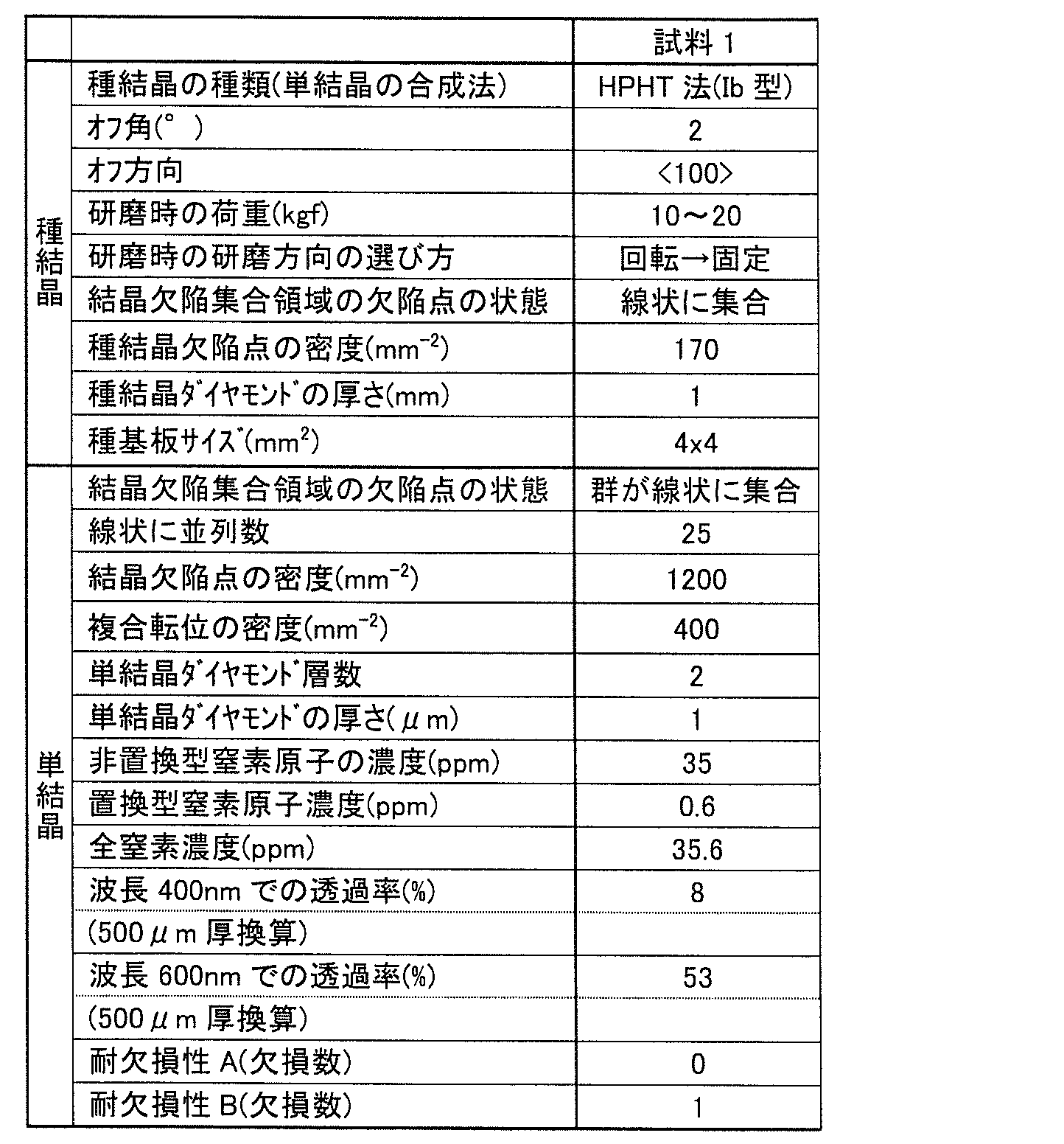
- a diamond seed crystal 10 substrate grown by a high-temperature high-pressure method was prepared as diamond seed crystal 10.
- the main surface 10 m had an off angle of 2 ° in the ⁇ 100> direction from the (001) plane, and the dimensions of the diamond seed crystal 10 were 4 mm ⁇ 4 mm ⁇ thickness 1 mm.
- the seed crystal is operated under conditions of a rotational speed of 500 rpm to 3000 rpm and a load of 10 kgf to 20 kgf.
- a polishing scratch extending linearly in the ⁇ 100> direction was formed as a defective linear assembly region (Sample 1).
- the load was gradually increased at a speed of 3 kgf / min or less, and the apparatus was equipped with a mechanism for suppressing the vibration of the grindstone so that the load does not exceed 52 kgf.
- the average particle diameter is an average particle diameter designated by a manufacturer that supplies a diamond polishing disk, and here, is an average particle diameter in the specifications of an international diamond polishing disk. This is generally determined by a method of selecting particles by sieving, and corresponds to approximately # 600 to # 1500.
- the energy of 300 keV to 10 MeV is 1 ⁇ 10 15 pieces ⁇ cm ⁇ 2 to 1 ⁇ 10 18 pieces ⁇ cm ⁇ 2 .
- a conductive layer region was formed by ion implantation of carbon at a dose. This step was performed in the case where the seed substrate and the single crystal diamond vapor-grown were separated by electrolytic etching. This step was omitted when diamond was sliced with a laser in a later step.
- single crystal diamond was grown by a microwave plasma CVD method on the main surface where the seed crystal defect linear aggregate region of each diamond seed crystal was formed.
- Hydrogen gas, methane gas, and nitrogen gas were used as the crystal growth gas, and the concentration of methane gas with respect to hydrogen gas was 5 mol% to 20 mol%, and the concentration of nitrogen gas with respect to methane gas was 0 to 5 mol%.
- the crystal growth pressure was 5 kPa to 15 kPa, and the crystal growth temperature (diamond seed crystal temperature) was 800 ° C. to 1200 ° C.
- each diamond seed crystal was separated from each single crystal diamond by electrolytic etching to decompose and remove the conductive layer region in the diamond seed crystal.
- the sample was sliced using a laser and separated from the seed substrate.
- the density of crystal defect points was 1200 mm -2
- the density of complex dislocations was 400 mm -2
- the number of single crystal diamond layers was 2
- the thickness of the single crystal diamond was 1.
- the concentration of 0 mm, non-substituted nitrogen atoms (nitrogen atoms not isolated) was 35 ppm.
- the density of crystal defect points and the density of complex dislocations were carried out as described in the [Crystal defects] column.
- the density of complex dislocations is the density at the crystal growth surface, and is measured as the point density at which the dislocations reach the surface.
- the single crystal diamond was processed into the shape of a cutter blade, the workpiece was cut, and the fracture resistance was evaluated. A series of evaluations and conditions are shown in Table 1.
- the cutting speed was 2000 m / min
- the depth of cut was 0.05 mm
- the feed amount was 0.05 mm / blade.
- the workpiece was made of aluminum material A5052, and after cutting the workpiece for 30 km, the fracture resistance was evaluated by the number of defects (number of defects) of 5 ⁇ m or more of the cutter blade (“Defect Resistance A (number of defects)” in Table 1). Went. As a result, the number of defects was zero and it was a very good single crystal diamond.
- the cutting speed was 2000 m / min
- the depth of cut was 0.10 mm
- the amount of feed was 0.10 mm / blade.
- the workpiece was made of aluminum material A5052, and after cutting the workpiece for 30 km, the fracture resistance was evaluated based on the number of defects (number of defects) of the cutter blade of 5 ⁇ m or more (“Defect Resistance B (number of defects)” in Table 1). Went. As a result, good fracture resistance results were obtained.
- the material is sufficiently usable as a product. More severe evaluation B is less than 5.
- the growth surface of the single crystal diamond was polished and evaluated by flattening.
- the evaluation result was the same as before polishing. That is, in the evaluation after polishing, the density of crystal defect points is 1200 mm ⁇ 2 , the density of complex dislocations is 400 mm ⁇ 2 , the number of single crystal diamond layers is 2, the thickness of single crystal diamond is 1.0 mm, the non-substitution type The concentration of nitrogen atoms (non-isolated nitrogen atoms) was 35 ppm.
- Single crystal diamond used a technique of performing ion etching and electrolytic etching in the step of separating from the seed substrate, but there was no significant difference in evaluation results depending on the method of slicing with laser. In the method of slicing with a laser, after evaluation, mechanical polishing was performed to form a normal flat surface, and then the next die chip was formed.
- This plate was cut to a desired size with a laser to form a die die for wire drawing, to produce a wire drawing die, and proceeded to the evaluation of the wire drawing die.
- a diamond die sample having the shape shown in FIGS. 1 to 3 was prepared.
- the single crystal diamond 20 is perpendicular to the main surface having an off angle of 2 ° from the ⁇ 001> direction, and parallel to the ⁇ 110> direction to the ⁇ 100> direction.
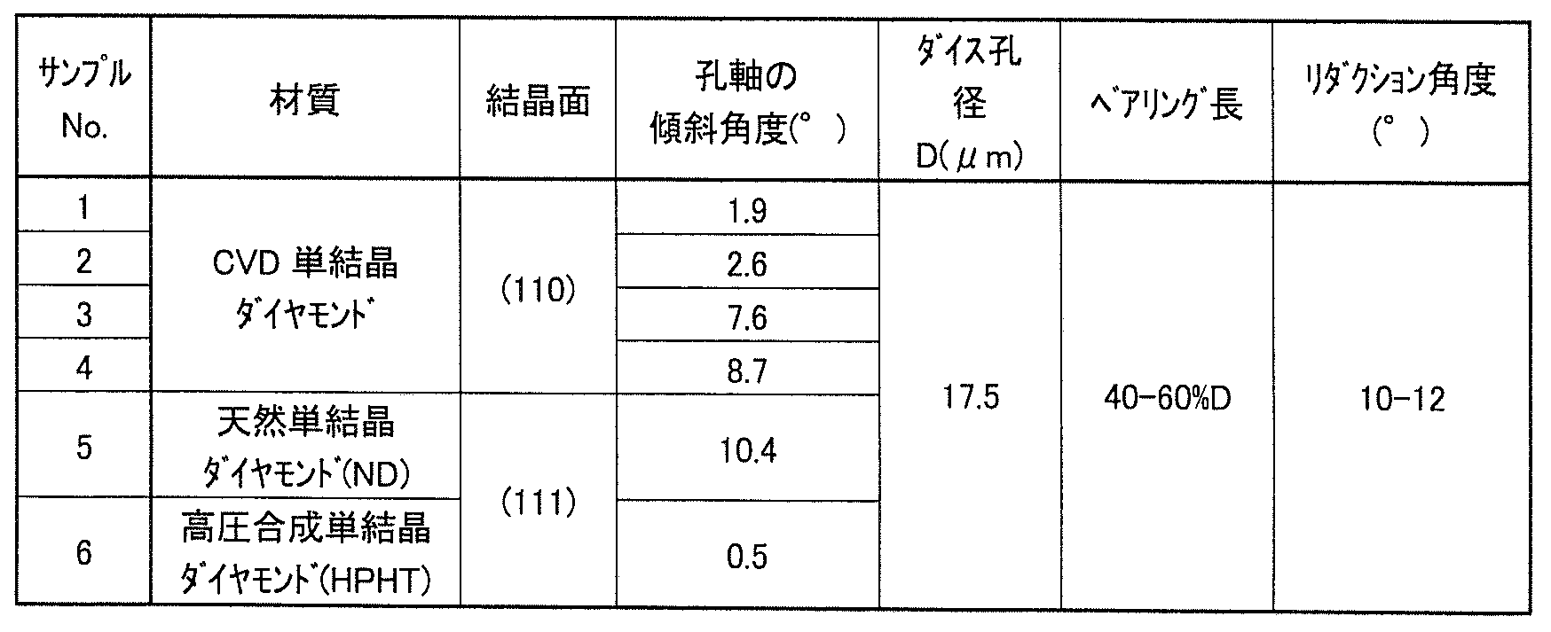
- the inclination angle of the hole axis is 1.9 °, 2.6 °, 7.6 °, and 8.7 °, respectively, from the ⁇ 1-10> direction.
- the drawing index is 1, where the drawing distance is 0.5 km.
- the lower left graph shows the amount of expansion of the die hole diameter when the wire is drawn by 1 km as the amount of wear.
- Sample No. which is the product of the present invention In the 1-4 die (CVD single crystal diamond, the upper and lower surfaces are (110) planes), the inclination angle was 0.1 to 15 °, and there was no wear that partly peeled off. The smaller the tilt angle, the less wear.
- Sample No. which is a comparative example In the case of No. 6 die (high-pressure synthetic single crystal diamond (HPHT), the upper and lower surfaces are (111) planes), the wear amount was larger than that of the present invention product.
- Sample No. which is a comparative example In the case of No. 5 die (natural single crystal diamond (ND), the upper and lower surfaces are (111) surfaces), the amount of wear was larger than that of the present invention product. When the inclination angle was 10.4 °, wear such that part of the film peeled off was observed.
- the wear amount is almost the same as that of the present invention, but the upper and lower surfaces are ( 110) surface diamond is difficult to manufacture, which increases costs.
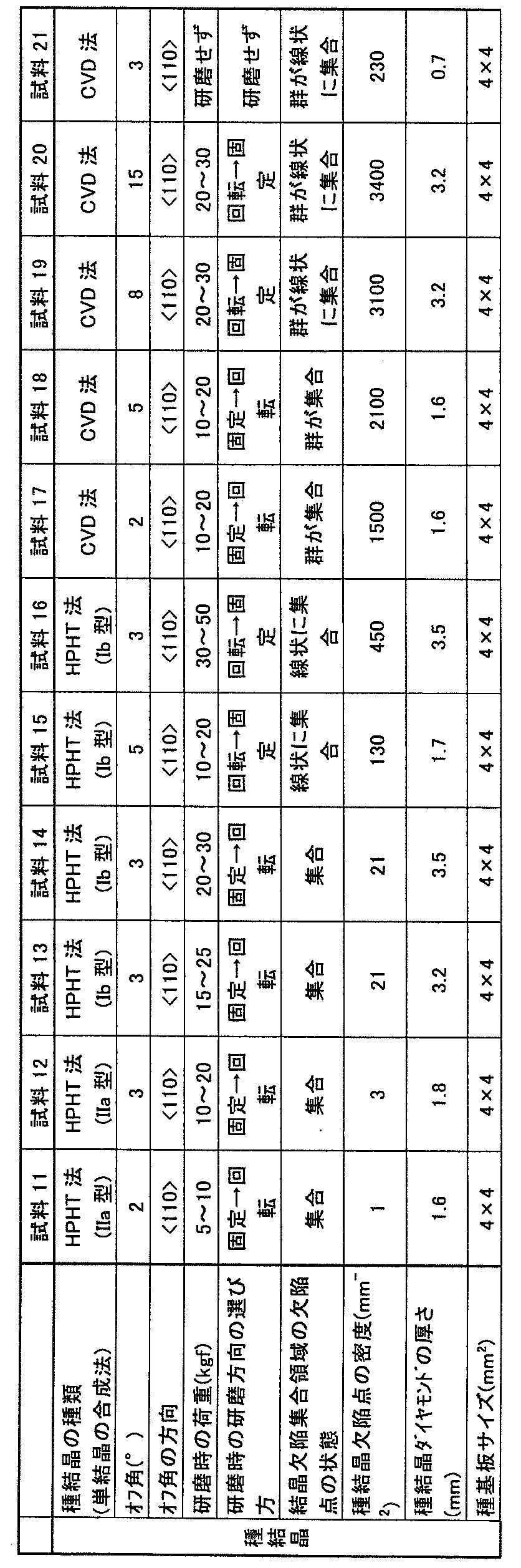
- Example 11 to Sample 21 A slightly different sample (Sample 11 to Sample 21) was prepared in the same procedure as in Example 1.
- the main surface has an off angle of 2 ° to 15 ° in the ⁇ 1-10> direction from the (001) plane, has an area of 4 mm ⁇ 4 mm, and has a thickness of 0.7 to 3.5 mm.
- a crystal substrate was prepared.
- the inclination angle of the hole axis was matched with the off-angle of the seed substrate shown in Table 3.
- the conditions for preparing the seed substrate were as shown in Example 1 except that they were shown in Table 3, and the single crystals shown in Table 4 were obtained.
- “Groups are gathered in a line” means that a group of groups is elongated and connected in a line.
- a “group” is a collection of crystal defect points based on crystal defect lines branched from the same starting point.
- “Crystal defect point of seed crystal” is a combination of the origin of a group of crystal defect lines in a single crystal layer and the origin of a crystal defect line that is not a group, and 70% of defect points in a specific range. Assume that the cases where the total sum of the defect point ranges can be limited to 50% of the area of the range when collected are collected. However, the defect point range is a range where one defect point range has a radius to the closest defect point. “Dotted” refers to a state in which the above definitions are not aggregated.
- the single crystal diamond 20 was processed into the shape of a cutter blade, the workpiece was cut, and the fracture resistance was evaluated.
- RF4080R manufactured by Sumitomo Electric Hardmetal Co., Ltd. was used as the cutter, and SNEW1204ADFR-WS was used as the wiper chip.
- the cutting speed was 2000 m / min, the depth of cut was 0.05 mm, and the feed amount was 0.05 mm / blade.
- the workpiece was an aluminum material A5052, and after cutting the workpiece for 30 km, the fracture resistance was evaluated (Evaluation A) by the number of defects (number of defects) of the cutter blade of 5 ⁇ m or more.
- the cutting speed was 2000 m / min
- the depth of cut was 0.10 mm
- the amount of feed was 0.10 mm / blade.
- aluminum material A5052 was used, and after cutting the workpiece for 30 km, the fracture resistance was evaluated (evaluation B) by the number of defects (number of defects) of the cutter blade of 5 ⁇ m or more. As a result, it is shown at the bottom of Table 4.
- this cut surface 202 was prepared by cutting into a rectangular parallelepiped so as to be a main surface (the upper surface 5 and the lower surface 6, the hole 14 being formed perpendicular to the main surface) on which the die hole 14 is formed, the inclination of the hole axis
- the dice samples A11 to A21 were manufactured by matching the angle with the off-angle of the seed substrate in Table 3 from the ⁇ 1-10> direction. Die samples A11 to A21 are composed of samples 11 to 21.
- the single crystal diamond having an off angle from the ⁇ 001> direction is used using the sample 12, the sample 17, the sample 20, and the sample 21.
- the surface was prepared by cutting into a rectangular parallelepiped so that the main surface forming the hole of the die (the hole was formed perpendicular to the main surface). In this case, the inclination angle of the hole axis coincided with the off-angle in Table 3 from the (001) plane (die samples B12, B17, B20, B21).
- the die samples B12, B17, B20, and B21 are composed of the samples 12, 17, 20, and 21, respectively.
- the single crystal diamond 20 is turned off from the ⁇ 001> direction as shown in FIG. Cut perpendicularly to the principal surface having the corners and parallel to the ⁇ 110> direction, and as shown in FIG. 17, perpendicular to the cut surface 203 and from the ⁇ 001> direction to the ⁇ 110> direction ⁇ 2 (54. 7 °: (1-10) in-plane angle) Cut perpendicular to the rotated direction. Since this cut surface was prepared by cutting into a rectangular parallelepiped so as to be a main surface for forming a die hole (the hole was formed perpendicular to the main surface), the inclination angle of the hole axis was 1.
- die samples C13, C18, and C19 were obtained (die samples C13, C18, and C19).
- the die samples C13, C18, and C19 are composed of samples 13, 18, and 19, respectively.
- the defect resistance is large in the preliminary evaluation, that is, when there are five or more defects in evaluation A, chipping occurs when the diamond die is manufactured, and the die cannot be manufactured.
- the samples of the example die samples A11 to A21 all exhibited wear resistance equivalent to the samples 1 to 4 in Table 2 of Example 1.
- the samples of the die samples B12, B17, B20, B21, C13, C18, and C19 of this example all had less wear than the samples 5 and 6 in Table 2 of Example 1.
- the metal part of the die was melted, the single crystal diamond was taken out, and the single crystal diamond chip with a hole was evaluated as to X-ray topography, SIMS, ESR, transmittance by microscope, and the like. As a result, the original characteristics shown in Tables 1 and 4 were confirmed for the dies produced from the diamond single crystal.
- the hole axis and crystal plane orientation can be confirmed by looking at the outline of multiple holes as seen through the hole axis direction with a microscope (the innermost circle that can be confirmed with the smallest diameter of the outermost circle and hole where the rectangular parallelepiped of the hole and the tip intersects) Evaluation was made by X-ray diffraction in a state where the substrate was fixed so that the direction in which the contours of the circles and the like became concentric were vertical. Evaluation of X-rays is the same as a general method for evaluating fluctuations, off angles, and pole figures of a plate-like single crystal. By making the perpendicular direction of the substrate coincide with the direction of the hole axis, the inclination angle of the hole axis can be confirmed.
Landscapes
- Chemical & Material Sciences (AREA)
- Engineering & Computer Science (AREA)
- Organic Chemistry (AREA)
- Materials Engineering (AREA)
- Metallurgy (AREA)
- Mechanical Engineering (AREA)
- General Chemical & Material Sciences (AREA)
- Chemical Kinetics & Catalysis (AREA)
- Crystallography & Structural Chemistry (AREA)
- Inorganic Chemistry (AREA)
- Crystals, And After-Treatments Of Crystals (AREA)
- Metal Extraction Processes (AREA)
- Carbon And Carbon Compounds (AREA)
- Chemical Vapour Deposition (AREA)
Abstract
Description
特許文献1では、単結晶ダイヤモンドを使用したダイスが記載されている。単結晶ダイヤモンドとして天然ダイヤモンドを使う場合、近年では高品質な天然ダイヤモンド素材を安定して入手できなくなっている問題がある。そのため、高温高圧合成ダイヤモンドなどの人造ダイヤモンドを使うことが考えられるが、人造ダイヤモンドを使用したダイヤモンドダイスは天然ダイヤモンドを使用したダイヤモンドダイスに比べると、伸線する線材の材質によっては孔の摩耗が大きく、寿命が短くなる場合があった。また、単結晶ダイヤモンドダイスの場合、結晶方位をどの方向にどのように設定するかにより、孔の摩耗が早くなるあるいは偏摩耗が発生しやすくなるなどの現象が現れ、ダイスの寿命が短くなることが起こり得る。
最初に本願発明の実施態様を列記して説明する。
図1は、この発明の実施の形態に従ったダイヤモンドダイスの平面図である。図2は、図1中のII-II線に沿った断面図である。図1および図2を参照して、ダイヤモンドダイス4は、中心に位置するダイヤモンド1と、ダイヤモンド1の周りに設けられたダイヤモンド1を保持する焼結合金2と、焼結合金2を保持するケース3とを有する。
ダイスを構成する単結晶ダイヤモンドは、以下の特性を有することが好ましい。この特性を有していなくてもよい。
図4および図5を参照して、本実施形態の単結晶ダイヤモンド20は、結晶成長主面20mについてのX線トポグラフィー像において結晶欠陥20dが存在する線を示す結晶欠陥線20dq(例えば転位線など)が単結晶ダイヤモンド20の少なくともある一つの面に達する先端の点である結晶欠陥点20dpの群が集合して存在する。ここで、欠陥点の群が集合するという表現は、本願発明では少し踏み込んだ内容である。つまり、結晶欠陥点は一つの起点から枝分かれした複数の欠陥点あるいはそれらの途中から枝分かれした欠陥点の集まりを一つの群とし、別の起点由来のものは別の群とする。従って、同じ群を全て包含する最小の円を群のエリアとすると、ある群のエリアと別の群のエリアが接触もしくは重なる場合に群が集合していると表現する。
ここで、結晶欠陥20dには、点欠陥、転位、欠損、亀裂、結晶歪みなどの各種の欠陥が含まれる。また、転位には、刃状転位、螺旋転位、複数の刃状転位および複数の螺旋転位の少なくともいずれかが複合した複合転位などが含まれる。
図7を参照して、本実施形態の単結晶ダイヤモンド20の製造方法は、主面10m上に種結晶欠陥点10dpが集合している種結晶欠陥集合領域を有するダイヤモンド種結晶10を準備する工程(図7(A))と、ダイヤモンド種結晶10の主面10m上に、化学気相堆積法により単結晶ダイヤモンド20を成長させる工程(図7(B))と、を備える。種結晶欠陥点とは、種基板における結晶欠陥点の意味であり、種結晶欠陥集合領域とは種基板に結晶欠陥点が集合している領域である。上記のダイヤモンド種結晶基板の主面上の種結晶欠陥集合領域は、種結晶欠陥点10dpの群が集合していることがより好ましく、種結晶欠陥点10dpが集合して線状に延びていることがさらに好ましく、種結晶欠陥点10dpの群が集合して線状に延びていることがもっと好ましい。
(種結晶欠陥集合領域を有するダイヤモンド)
図7(A)を参照して、主面10m上に種結晶欠陥点10dpの集合している種結晶欠陥集合領域を有するダイヤモンド種結晶10を準備する工程は、特に制限はないが、主面10m上に種結晶欠陥点10dpの群が集合して線状に延びる種結晶欠陥線状集合領域を有するダイヤモンド種結晶10を効率的に準備する観点から、ダイヤモンド種結晶10を準備するサブ工程と、ダイヤモンド種結晶10の主面10m上に種結晶欠陥点10dpが集合している種結晶欠陥集合領域を形成するサブ工程と、ダイヤモンド種結晶10の主面10m側に、イオンを注入することにより、イオン注入領域10cを形成するサブ工程と、を含むことができる。
図7(B)を参照して、単結晶ダイヤモンド20を成長させる工程は、ダイヤモンド種結晶10の主面10m上に、化学気相堆積(CVD)法により、単結晶ダイヤモンド20を成長させることにより行なう。CVD法としては、マイクロ波プラズマCVD法、DCプラズマCVD法、ホットフィラメントCVD法などが好適に用いられる。単結晶成長用ガスとしては、水素、メタン、アルゴン、窒素、酸素、二酸化炭素などを用いて、単結晶ダイヤモンド中の非孤立置換型窒素原子の濃度(全窒素原子濃度から孤立置換型窒素原子濃度を差し引いた濃度)が1ppm以上、より好ましくは5ppm以上、さらには8ppm以上になるように調整することが好ましい。さらに、ジボラン、トリメチルボロン、ホスフィン、ターシャルブチルリン、シランなどのドーピングガスを添加してもよい。単結晶ダイヤモンド20の結晶成長面が(100)面方位であることが好ましく、結晶成長初期の厚さが1μm~7μmの領域は、少なくとも成長パラメーター(α)が2以上かつダイヤモンド種結晶10の温度が1100℃以下で成長することが好ましい。成長パラメーター(α)とは、<111>方向の結晶成長速度に対する<100>方向の結晶成長速度の比を√3倍した値である。
図7(C)を参照して、本実施形態の単結晶ダイヤモンド20の製造方法は、効率よく単結晶ダイヤモンド20を得る観点から、ダイヤモンド種結晶10を分離する工程をさらに備えることができる。
(単結晶ダイヤモンドの追加成長工程)
図7(D)を参照して、本実施形態の単結晶ダイヤモンド20の製造方法は、大きな欠損の発生がさらに抑制される単結晶ダイヤモンド20を得る観点から、単結晶ダイヤモンド20を追加して成長させる工程をさらに備えることができる。
1.主面に種結晶欠陥線状集合領域を有するダイヤモンド種結晶の準備
図7(A)を参照して、ダイヤモンド種結晶10として、高温高圧法により成長させたダイヤモンド種結晶10の基板を準備した。主面10mが(001)面から<100>方向に2°のオフ角を有し、ダイヤモンド種結晶10の寸法は4mm×4mm×厚さ1mmであった。
次に、各々のダイヤモンド種結晶の種結晶欠陥線状集合領域が形成された主面上に、マイクロ波プラズマCVD法により、単結晶ダイヤモンドを成長させた。結晶成長用ガスとして、水素ガス、メタンガス、および窒素ガスを使用し、水素ガスに対するメタンガスの濃度を5モル%~20モル%、メタンガスに対する窒素ガスの濃度を0~5モル%とした。結晶成長圧力は5kPa~15kPaとし、結晶成長温度(ダイヤモンド種結晶の温度)は800℃~1200℃とした。
次に、各々の単結晶ダイヤモンドから各々のダイヤモンド種結晶を、電解エッチングにより、ダイヤモンド種結晶中の導電層領域を分解除去することにより、ダイヤモンド種結晶から分離した。あるいはイオン注入をしなかった場合にはレーザーを用いてスライスして、種基板から分離した。
上記の方法で製造されるCVD単結晶ダイヤモンド(試料1)を用いて、図1から3で示す形状のダイヤモンドダイスのサンプルを作成した。図8から図10で示すように、ダイスを形成する時は、単結晶ダイヤモンド20を<001>方向からオフ角2°を有する主面に垂直に、<110>方向に平行から<100>方向に主面内の角度θ1(0.5°、1.2°、6.2°、7.3°)戻した方向に切断し、この切断面201をダイスの孔を形成する主面(孔はこの主面に垂直に形成する)となるように直方体に切って準備する。この結果、孔軸の傾斜角度は<1-10>方向から、それぞれ1.9°、2.6°、7.6°、8.7°となる。
減面率:13%
伸線速度:500m/min
線材:SUS304
潤滑剤:合成油系潤滑剤
伸線後、ダイスの孔の拡大量を測定した。その結果を図11-13で示す。
左下のグラフは、1km伸線したときのダイス孔径の拡大量を摩耗量として示している。

単結晶ダイヤモンド20は、カッター刃の形状に加工し、ワークの切削加工を行って耐欠損性を評価した。カッターは住友電工ハードメタル株式会社製RF4080Rを用い、ワイパーチップは同SNEW1204ADFR-WSを用いた。旋盤は株式会社森精機製のNV5000を用いた。切削速度は2000m/min、切込量0.05mm、送り量0.05mm/刃とした。ワークはアルミ材A5052を用い、ワークを30km切削した後に、カッター刃の5μm以上の欠損の数(欠損数)により、耐欠損性の評価(評価A)を行った。また、別の少し強い条件で、切削速度は2000m/min、切込量0.10mm、送り量0.10mm/刃とした。ワークはアルミ材A5052を用い、ワークを30km切削した後に、カッター刃の5μm以上の欠損の数(欠損数)により、耐欠損性の評価(評価B)を行った。その結果、表4の最下段に示す。
上記の方法で製造されるCVD単結晶ダイヤモンド(試料11~試料21)を用いて、実施例1と同じように図1から3で示す形状のダイヤモンドダイスのサンプルを作成した。各々ダイスは、図14および図15で示すように単結晶ダイヤモンド20を<001>方向からオフ角を有する主面に垂直に、かつ<110>方向に平行に切断した。この切断面202をダイスの孔14を形成する主面(上面5および下面6であり、孔14はこの主面に垂直に形成)となるように直方体に切って準備したので、孔軸の傾斜角度は、<1-10>方向からの表3の種基板のオフ角に一致させてダイスサンプルA11~A21を製造した。ダイスサンプルA11からA21は、試料11から21で構成される。
Claims (17)
- 線材の伸線加工を行うための孔がダイヤモンドに設けられたダイヤモンドダイスであって、
前記ダイヤモンドは、CVD単結晶ダイヤモンドであり、
前記孔の軸は、前記ダイヤモンドの結晶面の法線方向に対し傾斜しているダイヤモンドダイス。 - 前記孔の軸は、前記ダイヤモンドの結晶面の法線方向に対し0.1~15°傾斜しているダイヤモンドダイス。
- 前記ダイヤモンドの上下面は、(110)面に対し0.1~15°傾斜した面である請求項1または2に記載のダイヤモンドダイス。
- 前記ダイヤモンドの上下面は、(100)面に対し0.1~15°傾斜した面である請求項1または2に記載のダイヤモンドダイス。
- 前記ダイヤモンドの上下面は、(111)面に対し0.1~15°傾斜した面である請求項1または2に記載のダイヤモンドダイス。
- 前記孔は、前記孔を規定するように、線材の流れの上流側から下流側に向かってリダクション部、直径Dのベアリング部、バックリリーフ部およびエクジット部を有し、
前記孔の軸に沿った断面における孔の形状において、前記ベアリング部の長さは0.4D以上1.5D以下である請求項1から5のいずれか一項に記載のダイヤモンドダイス。 - 前記直径Dが50μm未満であり、前記バックリリーフ部から前記エクジット部にかけての孔の断面形状は、凹形の曲線形状である請求項1から6のいずれか一項に記載のダイヤモンドダイス。
- 伸線加工を行う際の減面率を8%以上25%以下として使用される、請求項1から7のいずれか一項に記載のダイヤモンドダイス。
- 銅系金属線、鉄系金属線、金線、銀線、真鍮線、アルミニウム線、アルミニウム合金線、タングステン線などの金属線、またはこれらの線に各種金属めっきを行った線のいずれかの伸線加工に用いられる、請求項1から8のいずれか一項に記載のダイヤモンドダイス。
- 前記ダイヤモンドが、結晶成長主面についてのX線トポグラフィー像において結晶欠陥の存在を示す結晶欠陥線が前記結晶成長主面に達する先端の点である結晶欠陥点の群が集合して存在し、結晶欠陥点の密度が2mm-2より大きい単結晶ダイヤモンドを用いた、請求項1~9のいずれか一項に記載のダイヤモンドダイス。
- 前記結晶欠陥点のうち、複数の刃状転位および複数の螺旋転位の少なくともいずれかが複合した複合転位が結晶成長主面に達する先端の点である複合転位点の密度が2mm-2より大きい請求項10に記載のダイヤモンドダイス。
- 前記ダイヤモンドは、2つの主面と、その2つの主面の間に位置する複数の単結晶ダイヤモンド層とを含み、前記結晶欠陥線が2つの前記単結晶ダイヤモンド層の境界で複数に分岐し、片側の前記主面に向かって前記結晶欠陥線が増加している請求項10または11に記載のダイヤモンドダイス。
- 前記結晶欠陥点の群が線状に延びる結晶欠陥線状集合領域が複数並列して存在する請求項10~12のいずれか一項に記載のダイヤモンドダイス。
- 前記単結晶ダイヤモンド中の不純物原子として1ppm以上の窒素原子を含有し、前記窒素原子は孤立置換型窒素原子以外の窒素原子である請求項10~13のいずれか一項に記載のダイヤモンドダイス。
- 前記単結晶ダイヤモンドを500μm厚さで測定して、あるいは500μm厚さに換算して、400nmの光の透過率が60%以下の請求項10~14のいずれか一項に記載のダイヤモンドダイス。
- 前記孔の軸は、前記ダイヤモンドの結晶面の法線方向に対し1~8°傾斜している、請求項1から15のいずれか1項に記載のダイヤモンドダイス。
- 前記ダイヤモンドの結晶面は、(110)面、(100)面および(111)面のいずれかである、請求項1から16のいずれか1項に記載のダイヤモンドダイス。
Priority Applications (8)
| Application Number | Priority Date | Filing Date | Title |
|---|---|---|---|
| SG11201800522PA SG11201800522PA (en) | 2015-07-22 | 2016-07-22 | Diamond die |
| EP16827869.5A EP3326729B1 (en) | 2015-07-22 | 2016-07-22 | Diamond drawing die |
| MX2018000741A MX2018000741A (es) | 2015-07-22 | 2016-07-22 | Dado de diamante. |
| US15/745,849 US11007558B2 (en) | 2015-07-22 | 2016-07-22 | Diamond die |
| ES16827869T ES2777627T3 (es) | 2015-07-22 | 2016-07-22 | Matriz de embutir de diamante |
| JP2017529951A JP6545264B2 (ja) | 2015-07-22 | 2016-07-22 | ダイヤモンドダイス |
| KR1020187004566A KR20180033529A (ko) | 2015-07-22 | 2016-07-22 | 다이아몬드 다이스 |
| CN201680043048.8A CN107848002B (zh) | 2015-07-22 | 2016-07-22 | 金刚石拉丝模 |
Applications Claiming Priority (2)
| Application Number | Priority Date | Filing Date | Title |
|---|---|---|---|
| JP2015-145027 | 2015-07-22 | ||
| JP2015145027 | 2015-07-22 |
Publications (1)
| Publication Number | Publication Date |
|---|---|
| WO2017014309A1 true WO2017014309A1 (ja) | 2017-01-26 |
Family
ID=57834332
Family Applications (1)
| Application Number | Title | Priority Date | Filing Date |
|---|---|---|---|
| PCT/JP2016/071600 Ceased WO2017014309A1 (ja) | 2015-07-22 | 2016-07-22 | ダイヤモンドダイス |
Country Status (9)
| Country | Link |
|---|---|
| US (1) | US11007558B2 (ja) |
| EP (1) | EP3326729B1 (ja) |
| JP (1) | JP6545264B2 (ja) |
| KR (1) | KR20180033529A (ja) |
| CN (1) | CN107848002B (ja) |
| ES (1) | ES2777627T3 (ja) |
| MX (1) | MX2018000741A (ja) |
| SG (1) | SG11201800522PA (ja) |
| WO (1) | WO2017014309A1 (ja) |
Cited By (2)
| Publication number | Priority date | Publication date | Assignee | Title |
|---|---|---|---|---|
| JP2020518537A (ja) * | 2017-04-26 | 2020-06-25 | サンセット ピーク インターナショナル リミテッド | 大単結晶ダイヤモンドおよびその製造方法 |
| JP6996690B1 (ja) * | 2020-12-24 | 2022-01-17 | 住友電工ハードメタル株式会社 | ダイヤモンド工具中間体の製造方法および単結晶ダイヤモンドの判定方法 |
Families Citing this family (2)
| Publication number | Priority date | Publication date | Assignee | Title |
|---|---|---|---|---|
| WO2020004373A1 (ja) * | 2018-06-27 | 2020-01-02 | 住友電工ハードメタル株式会社 | 貫通孔付工具、ダイヤモンド部品、及び、ダイヤモンド素材 |
| JP7042989B1 (ja) * | 2020-10-22 | 2022-03-28 | 住友電工ハードメタル株式会社 | ダイヤモンド焼結体、及びダイヤモンド焼結体を備える工具 |
Citations (5)
| Publication number | Priority date | Publication date | Assignee | Title |
|---|---|---|---|---|
| JPH02268917A (ja) * | 1989-04-06 | 1990-11-02 | Sumitomo Electric Ind Ltd | 線引きダイス用素材および該素材を用いた線引きダイス |
| JP2002102917A (ja) * | 2000-09-27 | 2002-04-09 | Allied Material Corp | ダイヤモンドダイス |
| JP2006518699A (ja) * | 2003-02-19 | 2006-08-17 | エレメント シックス リミテッド | 摩耗用途のcvdダイヤモンド |
| JP2009518273A (ja) * | 2005-12-09 | 2009-05-07 | エレメント シックス テクノロジーズ (プロプライアタリー) リミテッド | 高結晶品質の合成ダイヤモンド |
| WO2016013588A1 (ja) * | 2014-07-22 | 2016-01-28 | 住友電気工業株式会社 | 単結晶ダイヤモンドおよびその製造方法、単結晶ダイヤモンドを含む工具、ならびに単結晶ダイヤモンドを含む部品 |
Family Cites Families (9)
| Publication number | Priority date | Publication date | Assignee | Title |
|---|---|---|---|---|
| JPS59229227A (ja) | 1983-06-08 | 1984-12-22 | Sumitomo Electric Ind Ltd | 合成ダイヤモンド単結晶を用いたダイス |
| US6007916A (en) | 1989-04-06 | 1999-12-28 | Sumitomo Electric Industries, Ltd. | Synthetic single crystal diamond for wiring drawing dies and process for producing the same |
| EP0391418B2 (en) * | 1989-04-06 | 1998-09-09 | Sumitomo Electric Industries, Ltd. | A diamond for a dresser |
| JPH04127913A (ja) | 1990-09-20 | 1992-04-28 | Asahi Daiyamondo Kogyo Kk | ダイヤモンドダイス |
| US5571236A (en) | 1992-08-28 | 1996-11-05 | Sumitomo Electric Industries, Ltd. | Diamond wire drawing die |
| JPH06170435A (ja) | 1992-08-28 | 1994-06-21 | Sumitomo Electric Ind Ltd | ダイヤモンド線引きダイスおよびダイヤモンド線引きダイスの製造方法 |
| US5636545A (en) * | 1995-07-07 | 1997-06-10 | General Electric Company | Composite diamond wire die |
| DE602006021467D1 (de) | 2005-12-09 | 2011-06-01 | Element Six Technologies Pty Ltd | Synthetischer diamant mit hoher kristalliner qualität |
| JPWO2008111215A1 (ja) | 2007-03-15 | 2010-06-24 | 株式会社アライドマテリアル | ダイヤモンドダイスおよびそれを用いた線材の製造方法 |
-
2016
- 2016-07-22 SG SG11201800522PA patent/SG11201800522PA/en unknown
- 2016-07-22 ES ES16827869T patent/ES2777627T3/es active Active
- 2016-07-22 EP EP16827869.5A patent/EP3326729B1/en active Active
- 2016-07-22 KR KR1020187004566A patent/KR20180033529A/ko not_active Abandoned
- 2016-07-22 JP JP2017529951A patent/JP6545264B2/ja active Active
- 2016-07-22 US US15/745,849 patent/US11007558B2/en active Active
- 2016-07-22 MX MX2018000741A patent/MX2018000741A/es unknown
- 2016-07-22 WO PCT/JP2016/071600 patent/WO2017014309A1/ja not_active Ceased
- 2016-07-22 CN CN201680043048.8A patent/CN107848002B/zh active Active
Patent Citations (5)
| Publication number | Priority date | Publication date | Assignee | Title |
|---|---|---|---|---|
| JPH02268917A (ja) * | 1989-04-06 | 1990-11-02 | Sumitomo Electric Ind Ltd | 線引きダイス用素材および該素材を用いた線引きダイス |
| JP2002102917A (ja) * | 2000-09-27 | 2002-04-09 | Allied Material Corp | ダイヤモンドダイス |
| JP2006518699A (ja) * | 2003-02-19 | 2006-08-17 | エレメント シックス リミテッド | 摩耗用途のcvdダイヤモンド |
| JP2009518273A (ja) * | 2005-12-09 | 2009-05-07 | エレメント シックス テクノロジーズ (プロプライアタリー) リミテッド | 高結晶品質の合成ダイヤモンド |
| WO2016013588A1 (ja) * | 2014-07-22 | 2016-01-28 | 住友電気工業株式会社 | 単結晶ダイヤモンドおよびその製造方法、単結晶ダイヤモンドを含む工具、ならびに単結晶ダイヤモンドを含む部品 |
Non-Patent Citations (1)
| Title |
|---|
| See also references of EP3326729A4 * |
Cited By (5)
| Publication number | Priority date | Publication date | Assignee | Title |
|---|---|---|---|---|
| JP2020518537A (ja) * | 2017-04-26 | 2020-06-25 | サンセット ピーク インターナショナル リミテッド | 大単結晶ダイヤモンドおよびその製造方法 |
| JP7256753B2 (ja) | 2017-04-26 | 2023-04-12 | サンセット ピーク インターナショナル リミテッド | 大単結晶ダイヤモンドおよびその製造方法 |
| JP6996690B1 (ja) * | 2020-12-24 | 2022-01-17 | 住友電工ハードメタル株式会社 | ダイヤモンド工具中間体の製造方法および単結晶ダイヤモンドの判定方法 |
| WO2022137429A1 (ja) * | 2020-12-24 | 2022-06-30 | 住友電工ハードメタル株式会社 | ダイヤモンド工具中間体の製造方法および単結晶ダイヤモンドの判定方法 |
| US11878354B2 (en) | 2020-12-24 | 2024-01-23 | Sumitomo Electric Hardmetal Corp. | Method of manufacturing diamond tool intermediate and method of making determination for single-crystal diamond |
Also Published As
| Publication number | Publication date |
|---|---|
| US11007558B2 (en) | 2021-05-18 |
| EP3326729A1 (en) | 2018-05-30 |
| US20180207697A1 (en) | 2018-07-26 |
| CN107848002A (zh) | 2018-03-27 |
| JP6545264B2 (ja) | 2019-07-17 |
| ES2777627T3 (es) | 2020-08-05 |
| EP3326729B1 (en) | 2020-02-26 |
| SG11201800522PA (en) | 2018-02-27 |
| KR20180033529A (ko) | 2018-04-03 |
| JPWO2017014309A1 (ja) | 2018-06-14 |
| EP3326729A4 (en) | 2019-02-20 |
| CN107848002B (zh) | 2020-03-13 |
| MX2018000741A (es) | 2018-05-15 |
Similar Documents
| Publication | Publication Date | Title |
|---|---|---|
| KR102392424B1 (ko) | 단결정 다이아몬드 및 그 제조 방법, 단결정 다이아몬드를 포함하는 공구, 및 단결정 다이아몬드를 포함하는 부품 | |
| US10280531B2 (en) | Diamond single crystal and production method thereof, and single crystal diamond tool | |
| JP6752143B2 (ja) | 合成単結晶ダイヤモンド、合成単結晶ダイヤモンドの製造方法及び合成単結晶ダイヤモンドを用いた工具 | |
| JP6118954B1 (ja) | 単結晶ダイヤモンド材、単結晶ダイヤモンドチップおよび穿孔工具 | |
| JP6545264B2 (ja) | ダイヤモンドダイス | |
| KR102653291B1 (ko) | 단결정 다이아몬드, 단결정 다이아몬드의 제조 방법 및 그것에 이용되는 화학 기상 퇴적 장치 | |
| JP7232186B2 (ja) | 単結晶ダイヤモンドおよびその製造方法 | |
| JP6228404B2 (ja) | ダイヤモンド複合体、ダイヤモンド接合体、単結晶ダイヤモンドおよびこれを備える工具 |
Legal Events
| Date | Code | Title | Description |
|---|---|---|---|
| 121 | Ep: the epo has been informed by wipo that ep was designated in this application |
Ref document number: 16827869 Country of ref document: EP Kind code of ref document: A1 |
|
| WWE | Wipo information: entry into national phase |
Ref document number: MX/A/2018/000741 Country of ref document: MX |
|
| ENP | Entry into the national phase |
Ref document number: 2017529951 Country of ref document: JP Kind code of ref document: A |
|
| WWE | Wipo information: entry into national phase |
Ref document number: 15745849 Country of ref document: US |
|
| NENP | Non-entry into the national phase |
Ref country code: DE |
|
| WWE | Wipo information: entry into national phase |
Ref document number: 11201800522P Country of ref document: SG |
|
| ENP | Entry into the national phase |
Ref document number: 20187004566 Country of ref document: KR Kind code of ref document: A |
|
| WWE | Wipo information: entry into national phase |
Ref document number: 2016827869 Country of ref document: EP |