WO2017017772A1 - Élément de production d'énergie photovoltaïque et son procédé de fabrication - Google Patents
Élément de production d'énergie photovoltaïque et son procédé de fabrication Download PDFInfo
- Publication number
- WO2017017772A1 WO2017017772A1 PCT/JP2015/071295 JP2015071295W WO2017017772A1 WO 2017017772 A1 WO2017017772 A1 WO 2017017772A1 JP 2015071295 W JP2015071295 W JP 2015071295W WO 2017017772 A1 WO2017017772 A1 WO 2017017772A1
- Authority
- WO
- WIPO (PCT)
- Prior art keywords
- semiconductor layer
- collector electrode
- amorphous semiconductor
- type
- transparent conductive
- Prior art date
- Legal status (The legal status is an assumption and is not a legal conclusion. Google has not performed a legal analysis and makes no representation as to the accuracy of the status listed.)
- Ceased
Links
Images


Classifications
-
- H—ELECTRICITY
- H10—SEMICONDUCTOR DEVICES; ELECTRIC SOLID-STATE DEVICES NOT OTHERWISE PROVIDED FOR
- H10F—INORGANIC SEMICONDUCTOR DEVICES SENSITIVE TO INFRARED RADIATION, LIGHT, ELECTROMAGNETIC RADIATION OF SHORTER WAVELENGTH OR CORPUSCULAR RADIATION
- H10F77/00—Constructional details of devices covered by this subclass
- H10F77/20—Electrodes
-
- Y—GENERAL TAGGING OF NEW TECHNOLOGICAL DEVELOPMENTS; GENERAL TAGGING OF CROSS-SECTIONAL TECHNOLOGIES SPANNING OVER SEVERAL SECTIONS OF THE IPC; TECHNICAL SUBJECTS COVERED BY FORMER USPC CROSS-REFERENCE ART COLLECTIONS [XRACs] AND DIGESTS
- Y02—TECHNOLOGIES OR APPLICATIONS FOR MITIGATION OR ADAPTATION AGAINST CLIMATE CHANGE
- Y02P—CLIMATE CHANGE MITIGATION TECHNOLOGIES IN THE PRODUCTION OR PROCESSING OF GOODS
- Y02P70/00—Climate change mitigation technologies in the production process for final industrial or consumer products
- Y02P70/50—Manufacturing or production processes characterised by the final manufactured product
Definitions
- the present invention relates to a photovoltaic device and a manufacturing method thereof.
- solar cells have attracted particular attention as clean power generation means that does not generate CO 2 or other greenhouse gases, or as power generation means with high operational safety that can replace nuclear power generation.
- One type of solar cell is a heterojunction solar cell with high power generation efficiency.
- Such a heterojunction solar cell includes, for example, a first intrinsic amorphous semiconductor layer, a p-type amorphous semiconductor layer, and a first transparent conductive film on one surface side of an n-type crystal semiconductor substrate.
- a first intrinsic amorphous semiconductor layer, a p-type amorphous semiconductor layer, and a first transparent conductive film on one surface side of an n-type crystal semiconductor substrate.
- the second intrinsic amorphous semiconductor layer, the n-type amorphous semiconductor layer, and the second transparent conductive film are stacked in this order on the other surface side of the n-type crystal semiconductor substrate.
- a collecting electrode for collecting the generated electricity is disposed on each outer surface of the first transparent conductive film and the second transparent conductive film.
- the collecting electrode on the incident surface (surface) side is generally composed of linear finger electrodes arranged in parallel and a strip-shaped bus bar electrode orthogonal to these finger electrodes.
- the collector electrode on the back surface side is formed of a metal film in consideration of current collecting properties and reflecting light that is transmitted without being absorbed (see International Publication No. 2012/105148).
- a metal film pure silver is preferably used because of the high reflectance of light having a wavelength in the near-infrared region that is transmitted and the excellent electrical conductivity.
- the collector electrode film on the back side is made of pure silver, the output characteristics will deteriorate unless the thickness is made larger than 60 nm. Therefore, it is necessary to form a film having a thickness exceeding 60 nm, which is a factor of high cost.
- the present invention has been made based on the circumstances as described above, and an object of the present invention is to provide a photovoltaic element capable of reducing the thickness of the collector electrode on the back side while maintaining the output characteristics, and a method for manufacturing the photovoltaic element. Is to provide.
- the present invention which has been made to solve the above problems, includes a p-type or n-type crystal semiconductor substrate and a first intrinsic amorphous semiconductor layer stacked on the one surface side of the crystal semiconductor substrate in the following order.
- a photovoltaic device comprising a semiconductor layer, an n-type amorphous semiconductor layer, a second transparent conductive film, and a second collector electrode, wherein one of the first collector electrode and the second collector electrode Is a metal film containing silver, at least one of palladium and gallium, and copper.
- the collector electrode on the back side of the first collector electrode and the second collector electrode is made of a metal film containing silver, at least one of palladium and gallium, and copper. It is configured.
- a metal film having such a composition By using a metal film having such a composition, a decrease in output characteristics can be suppressed even when the thickness is reduced to 60 nm or less.
- the inventors have found that the passivation ability of the intrinsic amorphous semiconductor layer that suppresses carrier recombination is improved by annealing.
- the metal film island crystals are agglomerated due to the grain growth of the metal (such as silver) by the annealing treatment.
- the agglomeration of the island crystals a portion where the film thickness is locally reduced appears in the metal film, and the conductivity of the metal film is lowered.
- the collector electrode is formed of silver, it is necessary to make the film thickness sufficiently thick so as not to be affected by aggregation in order to exhibit sufficient output characteristics.
- the metal film when the metal film is formed thick, the manufacturing cost increases.
- the collector electrode when the collector electrode is a metal film containing silver, at least one of palladium and gallium, and copper as in the present invention, these dopant species suppress grain growth, and Aggregation is suppressed. Therefore, by using a metal film having such a composition, it is possible to reduce the cost associated with the thinning of the collector electrode while maintaining the output characteristics.
- the average thickness of the metal film is preferably 15 nm or more and 60 nm or less. By setting the average thickness of the metal film within the above range, the metal film can be sufficiently thinned while suppressing a decrease in output characteristics.
- the photovoltaic element is preferably subjected to an annealing treatment.
- the annealing treatment By the annealing treatment, the passivation ability of the intrinsic amorphous semiconductor layer is increased.
- the conductivity of the metal film included in the photovoltaic element is not easily lowered by the annealing treatment. Therefore, the output characteristics of the photovoltaic device can be enhanced by the annealing treatment.
- the method of manufacturing a photovoltaic device is a photovoltaic device.
- the collector electrode on the back surface side is a metal film containing silver, at least one of palladium and gallium, and copper, and is annealed to maintain the output characteristics while maintaining the output characteristics.
- a photovoltaic device in which the side collector electrode is made thinner can be manufactured.
- the “amorphous” in the amorphous semiconductor layer includes not only a completely amorphous material but also a material having microcrystals in the amorphous material.
- “Intrinsic” in an intrinsic amorphous semiconductor layer means that impurities are not intentionally doped, and includes impurities that are originally contained in raw materials or impurities that are unintentionally mixed in the manufacturing process. Meaning.
- “Average thickness” means an average value of thicknesses measured at arbitrary ten points.
- the “main component” means a component having the highest content on a mass basis.
- the collector electrode on the back side can be made thinner while maintaining the output characteristics.
- the photovoltaic device manufacturing method of the present invention it is possible to manufacture a photovoltaic device in which the collector electrode on the back surface side is made thin while maintaining the output characteristics. Therefore, according to the photovoltaic device manufacturing method of the present invention, the manufacturing cost of the photovoltaic device can be reduced.
- FIG. 1 is a schematic cross-sectional view of a photovoltaic device according to an embodiment of the present invention.
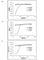
- A is a graph which shows the short circuit current of the photovoltaic device in an Example.
- B is a graph which shows the curve factor of the photovoltaic device in an Example.
- C is a graph which shows the conversion efficiency of the photovoltaic device in an Example.
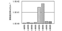
- FIG. 3 is a graph showing the results of contact resistance measurement in the example.
- FIG. 4 is a schematic diagram showing a film thickness measurement method.
- the photovoltaic device 10 of FIG. 1 includes an n-type crystal semiconductor substrate 11 and a first intrinsic amorphous system laminated on one surface side (upper side in FIG. 1) of the n-type crystal semiconductor substrate 11 in the following order.
- the semiconductor layer 12, the p-type amorphous semiconductor layer 13, the first transparent conductive film 14, the first collector electrode 15, and the other surface side (lower side in FIG. 1) of the n-type crystal semiconductor substrate 11 are A second intrinsic amorphous semiconductor layer 16, an n-type amorphous semiconductor layer 17, a second transparent conductive film 18, and a second collector electrode 19.
- the “outer surface” refers to the surface opposite to the n-type crystal semiconductor substrate 11 with the n-type crystal semiconductor substrate 11 as the center. Further, the “inner surface” refers to a surface on the n-type crystal semiconductor substrate 12 side.
- the n-type crystal semiconductor substrate 11 is formed from an n-type crystal semiconductor.
- An n-type crystal semiconductor is usually a crystal formed by adding a trace amount of a pentavalent element to a semiconductor such as silicon.
- Examples of the crystal semiconductor constituting the n-type crystal semiconductor substrate 11 include SiC and SiGe in addition to silicon (Si), but silicon is preferable from the viewpoint of productivity.
- the n-type crystal semiconductor substrate 11 may be a single crystal or a polycrystal.
- a pyramidal fine concavo-convex structure is formed on both surfaces of the n-type crystal semiconductor substrate 11.
- the height and size of the uneven structure may be uneven, and adjacent uneven parts may overlap.
- a vertex and a trough part may be roundish.
- the height of the unevenness is about several ⁇ m to several tens of ⁇ m.
- Such a concavo-convex structure can be obtained, for example, by immersing the substrate material in an etching solution containing about 1 to 5% by mass of sodium hydroxide and anisotropically etching the (100) plane of the substrate material.
- the average thickness of the n-type crystal semiconductor substrate 11 is not particularly limited.
- the upper limit of the average thickness is, for example, 300 ⁇ m, and preferably 200 ⁇ m. Moreover, as this minimum, it can be set as 50 micrometers, for example.
- the first intrinsic amorphous semiconductor layer 12 and the second intrinsic amorphous semiconductor layer 16 are usually made of silicon. With such an intrinsic amorphous semiconductor layer, carrier recombination can be suppressed and output characteristics can be improved.
- the average thickness of the first intrinsic amorphous semiconductor layer 12 and the second intrinsic amorphous semiconductor layer 16 can be, for example, 1 nm or more and 10 nm or less.
- the p-type amorphous semiconductor layer 13 is usually an amorphous layer formed by adding a small amount of a trivalent element to silicon.
- the average thickness of the p-type amorphous semiconductor layer 13 can be, for example, 1 nm or more and 20 nm or less.
- the n-type amorphous semiconductor layer 17 is usually an amorphous layer obtained by adding a trace amount of a pentavalent element to silicon.
- the average thickness of the n-type amorphous semiconductor layer 17 can be, for example, 1 nm or more and 20 nm or less.
- Examples of the transparent conductive material constituting the first transparent conductive film 14 and the second transparent conductive film 18 include indium tin oxide (ITO), indium tungsten oxide (IWO), indium cerium oxide (ICO), Aluminum zinc oxide (AZO), gallium zinc oxide (GZO), and the like can be given. Although it does not restrict
- the first collector electrode 15 disposed on the surface side, that is, the light incident surface side includes, for example, a plurality of linear finger electrodes arranged in parallel, and a plurality of strip-shaped bus bar electrodes orthogonal to the finger electrodes. Consists of In addition, the 1st collector electrode 15 may be comprised only from the finger electrode, for example.
- the first collector electrode is made of a conductive material. As this conductive material, a conductive adhesive such as a silver paste or a metal conductive wire such as a copper wire can be used.
- the width of each finger electrode is, for example, about 10 ⁇ m or more and 300 ⁇ m or less.
- the interval between the finger electrodes is, for example, about 0.5 mm to 4 mm.
- the width of each bus bar electrode is, for example, about 0.5 mm to 2 mm.
- the second collector electrode 19 disposed on the back side is a metal film containing silver (Ag), at least one of palladium (Pd) and gallium (Ga), and copper (Cu).
- the second collector electrode 19 is laminated on the entire outer surface of the second transparent conductive film 18.
- the photovoltaic element 10 can maintain good output characteristics even when the second collector electrode 19 on the back surface is a metal film containing such an element, even when it is thinned. The reason for this is that the second collector electrode 19 containing these elements is less likely to cause aggregation of silver island crystals during the annealing process, and during the annealing process caused by the adjacent second transparent conductive film 18. This is presumably due to the fact that oxidation hardly occurs.
- the second collector electrode 19 is preferably made of an Ag—Pd—Cu-based or Ag—Ga—Cu-based silver alloy containing Ag as a main component and added with at least one of Pd and Ga and Cu.
- the second collector electrode 19 may contain both Pd and Ga, and the total content of Pd and Ga can be, for example, 0.5 atomic% or more and 5 atomic% or less.
- the second collector electrode 19 As content of Cu in the 2nd collector electrode 19, it is 0.1 atomic% or more and 5 atomic% or less, for example. Since the second collector electrode 19 is formed of a silver alloy having such a composition, a decrease in conductivity due to the annealing treatment is further suppressed. The second collector electrode 19 may contain other components as long as the effects of the present invention are not impaired.
- the average thickness of the second collector electrode 19 (metal film) is not particularly limited, but the lower limit is preferably 15 nm, for example, and more preferably 30 nm.
- the upper limit may be, for example, 100 nm, but is preferably 60 nm, and more preferably 50 nm. Further, this upper limit may be 40 nm or 30 nm.
- the light incident surface is on the first collector electrode 15 side.
- the photovoltaic elements 10 are usually used by connecting a plurality thereof in series. By using a plurality of photovoltaic elements 10 connected in series, the generated voltage can be increased.
- the photovoltaic element 10 includes, for example, an n-type crystal semiconductor substrate 11, a first intrinsic amorphous semiconductor layer 12 stacked in the following order on one surface side of the crystal semiconductor substrate 11, a p-type amorphous A semiconductor layer 13 and a first transparent conductive film 14; a second intrinsic amorphous semiconductor layer 16 stacked on the other surface of the crystalline semiconductor substrate 11 in the following order; an n-type amorphous semiconductor layer; A step (a) of obtaining a layered structure including the semiconductor layer 17 and the second transparent conductive film 18; A step (b) of laminating a metal film containing silver, at least one of palladium and gallium, and copper on one outer surface of the layer structure; A step (c) of forming the first collector electrode 15 on the other outer surface of the layer structure, and a step (d) of annealing the layer structure in which the metal film is laminated. It can obtain suitably by a manufacturing method provided with.
- the step (a) is a step of laminating the first intrinsic amorphous semiconductor layer 12 on one surface side of the n-type crystal semiconductor substrate 11, and further, the p-type amorphous semiconductor layer 13 is formed.
- a step of laminating, a step of laminating the first transparent conductive film 14, a step of laminating the second intrinsic amorphous semiconductor layer 16 on the other surface side of the n-type crystal semiconductor substrate 11, and an n-type amorphous semiconductor A step of laminating the crystalline semiconductor layer 17 and a step of laminating the second transparent conductive film 18.
- the order of the steps is not particularly limited as long as the desired layer structure can be obtained.
- Examples of a method for stacking the first intrinsic amorphous semiconductor layer 12 and the second intrinsic amorphous semiconductor layer 16 include known methods such as chemical vapor deposition.
- Examples of chemical vapor deposition include plasma CVD and catalytic CVD (also called hot wire CVD).
- a mixed gas of SiH 4 and H 2 can be used as the source gas.
- the p-type amorphous semiconductor layer 13 and the n-type amorphous semiconductor layer 17 are stacked by a known method such as chemical vapor deposition similar to the stacking of the intrinsic amorphous semiconductor layer.
- a film can be formed.
- a mixed gas of SiH 4 , H 2, and B 2 H 6 can be used as the source gas.
- a mixed gas of SiH 4 , H 2, and PH 3 can be used.
- Examples of the method of laminating the first transparent conductive film 14 and the second transparent conductive film 18 include a sputtering method, a vacuum deposition method, an ion plating method (reactive plasma deposition method), and the like. And the ion plating method are preferred.
- the sputtering method is excellent in film thickness controllability and the like, and can be performed at a lower cost than the ion plating method.
- the ion plating method it is possible to perform film formation while suppressing generation of defects.
- Step (b) In the step (b), a metal film containing silver, at least one of palladium and gallium, and copper is laminated on one outer surface of the layer structure, that is, the outer surface of the second transparent conductive film 18. .
- This metal film becomes the second collector electrode 19.
- it does not specifically limit as a lamination
- This sputtering can be performed using a sputtering target having the same composition as the desired second collector electrode 19.
- a film may be formed by using a sputtering target of each element constituting the second collector electrode 19 and simultaneously performing sputtering while controlling the discharge amount.
- the first collector electrode 15 is formed on the other outer surface of the layer structure, that is, the outer surface of the first transparent conductive film 14.
- the first collector electrode 15 can be formed by a printing method such as screen printing or gravure offset printing when a conductive adhesive is used as a forming material.
- the first collector electrode 15 is formed by fixing it on the first transparent conductive film 14 with a conductive adhesive or a low melting point metal (solder or the like). can do.
- the first collector electrode 15 may be formed by plating or the like.
- Step (d) In the step (d), the layer structure on which the metal film is laminated is annealed. By performing such annealing, the passivation ability of the first intrinsic amorphous semiconductor layer 12 and the like can be improved, and the output characteristics of the heterojunction photoelectric conversion element can be improved. Further, the first collector electrode 15 can be dried and cured when formed by a printing method. On the other hand, the second collector electrode 19 (metal film) is also annealed during this annealing, but is formed from an alloy containing silver, at least one of palladium and gallium, and copper. Aggregation of crystals and the like are suppressed, and conductivity is not greatly reduced. Therefore, the output characteristics of the photovoltaic device 10 obtained can be improved by this annealing treatment.
- the conditions for the annealing treatment are not particularly limited, but for example, the lower limit of the treatment temperature can be 150 ° C., and 180 ° C. is preferable.
- the upper limit may be 300 ° C., preferably 250 ° C.
- the upper limit is preferably 1 hour, and more preferably 40 minutes.
- the present invention is not limited to the above-described embodiment, and the configuration can be changed without changing the gist of the present invention.
- the structure of the first collector electrode and the second collector electrode is reversed, and the lower side (second transparent conductive film side) in FIG.
- a power generation element may be used.
- a p-type crystal semiconductor substrate may be used instead of the n-type crystal semiconductor substrate.
- Example 1 First transparent conductive film / p-type amorphous silicon layer / first intrinsic amorphous silicon layer / n-type crystalline silicon substrate / second intrinsic amorphous silicon layer / n-type amorphous system A layer structure composed of silicon layer / second transparent conductive film was prepared.
- n-type crystal silicon substrate a single crystal substrate having a fine concavo-convex structure (texture structure) having innumerable pyramid shapes on both surfaces was used. This concavo-convex structure was formed by immersing the substrate material in an etching solution containing about 3% by mass of sodium hydroxide and anisotropically etching the (100) plane of the substrate material.
- Each silicon layer was laminated by a plasma CVD method.
- Each transparent conductive film was laminated by sputtering using indium oxide containing 3% by mass of tin oxide (a sputtering target of Umicore).
- the p-type amorphous silicon layer, the first intrinsic amorphous silicon layer, the n-type crystalline silicon substrate, the second intrinsic amorphous silicon layer, and the n-type amorphous silicon layer are respectively It corresponds to a p-type amorphous semiconductor layer, a first intrinsic amorphous semiconductor layer, an n-type crystal semiconductor substrate, a second intrinsic amorphous semiconductor layer, and an n-type amorphous semiconductor layer.
- a metal film made of an Ag—Pd—Cu based alloy was formed on the outer surface of the second transparent conductive film on the back side by sputtering using an APC-TR target manufactured by Furuya Metal Co., Ltd.
- a linear collector electrode was formed on the outer surface of the first transparent conductive film on the surface side by a printing method using a silver paste.
- annealing treatment at 200 ° C. for 30 minutes was performed to obtain the photovoltaic device of the example.
- a plurality of types in which the average thickness of the metal film (collector electrode) was changed between 15 nm and 130 nm were produced.
- Example 2 An AGC target (Ag: 97.0 to 99.7% by mass, Ga: 0.2 to 1.5% by mass, Cu: 0.1 to 1.5%) is formed on the outer surface of the second transparent conductive film on the back side.
- the photovoltaic device of Example 2 was obtained in the same manner as in Example 1 except that a metal film made of an Ag—Ga—Cu alloy was formed by sputtering. In the same manner as in Example 1, a plurality of types in which the average thickness of the metal film (collector electrode) was changed between 15 nm and 130 nm were produced.
- a photovoltaic device of a comparative example was obtained in the same manner as in the example except that a metal film made of pure silver was formed by sputtering on the outer surface of the second transparent conductive film on the back side. Similar to Examples 1 and 2, a plurality of types in which the average thickness of the metal film (collector electrode) was changed between 15 nm and 130 nm were produced.
- test film (average thickness 50 nm) was formed on the surface of the transparent conductive film made of indium oxide containing 3% by mass of tin oxide by sputtering, and then annealed (200 ° C., 30 minutes). The contact resistivity of each test film before and after annealing was measured. The measurement results are shown in FIG.
- the test films 1 and 2 (Ag—Pd—Cu alloy film) were formed using the APC-TR target used in Example 1.
- Test films 3 and 4 (Ag—Ga—Cu alloy films) were formed using the AGC target used in Example 2.
- Test film 1 Ag—Pd—Cu alloy (before annealing)
- Test film 2 Ag—Pd—Cu alloy (after annealing)
- Test film 3 Ag—Ga—Cu alloy (before annealing)
- Test film 4 Ag—Ga—Cu alloy (after annealing)
- Test film 5 Al—Ni alloy (before annealing)
- Test film 6 Al—Ni alloy (after annealing)
- Test film 8 Mo (after annealing) All annealing treatments were performed at 200 ° C. for 30 minutes.
- the thickness of the metal film or the like refers to the thickness in the direction perpendicular to the surface of each layer or film.
- FIG. 4 showing the virtual substrate 50 will be described.
- the substrate 50 in FIG. 4 has both the smooth part 51 and the uneven part 52.
- TEM transmission electron microscope
- TEM transmission electron microscope
- the photovoltaic device of the present invention can reduce the thickness of the collector electrode on the back side while maintaining output characteristics, and can be suitably used for photovoltaic power generation.
Landscapes
- Photovoltaic Devices (AREA)
Abstract
L'invention concerne : un élément de production d'énergie photovoltaïque dans lequel une électrode collectrice sur le côté surface arrière peut être formée en un film mince, tout en maintenant des caractéristiques de sortie ; et un procédé de fabrication de l'élément de production d'énergie photovoltaïque. Un élément de production d'énergie photovoltaïque selon la présente invention est pourvu : d'un substrat semi-conducteur cristallin de type p ou de type n ; d'une première couche semi-conductrice amorphe intrinsèque, d'une couche semi-conductrice amorphe de type p, d'un premier film conducteur transparent, et d'une première électrode collectrice, qui sont stratifiés dans cet ordre sur un côté surface du substrat semi-conducteur cristallin ; et d'une première couche semi-conductrice amorphe intrinsèque, d'une couche semi-conductrice amorphe de type n, d'un second film conducteur transparent, et d'une seconde électrode collectrice, qui sont stratifiés dans cet ordre sur l'autre côté surface du substrat semi-conducteur cristallin. L'élément de production d'énergie photovoltaïque est caractérisé en ce que la première électrode collectrice ou la seconde électrode collectrice est un film métallique contenant de l'argent, du cuivre, et du palladium et/ou du gallium. L'épaisseur moyenne du film métallique est de préférence de 15 à 60 nm. Il est préférable que l'élément de production d'énergie photovoltaïque soit recuit.
Priority Applications (3)
| Application Number | Priority Date | Filing Date | Title |
|---|---|---|---|
| PCT/JP2015/071295 WO2017017772A1 (fr) | 2015-07-27 | 2015-07-27 | Élément de production d'énergie photovoltaïque et son procédé de fabrication |
| JP2015560469A JP5987127B1 (ja) | 2015-07-27 | 2015-07-27 | 光発電素子及びその製造方法 |
| TW105123721A TW201709541A (zh) | 2015-07-27 | 2016-07-27 | 光發電元件及其製造方法 |
Applications Claiming Priority (1)
| Application Number | Priority Date | Filing Date | Title |
|---|---|---|---|
| PCT/JP2015/071295 WO2017017772A1 (fr) | 2015-07-27 | 2015-07-27 | Élément de production d'énergie photovoltaïque et son procédé de fabrication |
Publications (1)
| Publication Number | Publication Date |
|---|---|
| WO2017017772A1 true WO2017017772A1 (fr) | 2017-02-02 |
Family
ID=56871714
Family Applications (1)
| Application Number | Title | Priority Date | Filing Date |
|---|---|---|---|
| PCT/JP2015/071295 Ceased WO2017017772A1 (fr) | 2015-07-27 | 2015-07-27 | Élément de production d'énergie photovoltaïque et son procédé de fabrication |
Country Status (3)
| Country | Link |
|---|---|
| JP (1) | JP5987127B1 (fr) |
| TW (1) | TW201709541A (fr) |
| WO (1) | WO2017017772A1 (fr) |
Families Citing this family (2)
| Publication number | Priority date | Publication date | Assignee | Title |
|---|---|---|---|---|
| CN107924957A (zh) * | 2015-09-09 | 2018-04-17 | 夏普株式会社 | 太阳能电池及太阳能电池的制造方法 |
| TWI632690B (zh) * | 2017-06-30 | 2018-08-11 | 茂迪股份有限公司 | 半導體基板、太陽能電池、太陽能電池模組、半導體晶棒切割方法、半導體晶棒切割裝置 |
Citations (5)
| Publication number | Priority date | Publication date | Assignee | Title |
|---|---|---|---|---|
| JPH1117202A (ja) * | 1997-06-26 | 1999-01-22 | Kyocera Corp | 太陽電池素子 |
| JP2003297158A (ja) * | 2002-04-01 | 2003-10-17 | Canon Inc | グリッド電極を有する透明導電膜及びその製造方法 |
| JP2006295197A (ja) * | 2005-04-14 | 2006-10-26 | E I Du Pont De Nemours & Co | 導電性厚膜組成物、それから形成される電極および太陽電池 |
| WO2012001857A1 (fr) * | 2010-06-21 | 2012-01-05 | 三菱電機株式会社 | Dispositif photovoltaïque |
| JP2014241392A (ja) * | 2012-10-02 | 2014-12-25 | 株式会社カネカ | 結晶シリコン太陽電池の製造方法、太陽電池モジュールの製造方法、結晶シリコン太陽電池並びに太陽電池モジュール |
Family Cites Families (1)
| Publication number | Priority date | Publication date | Assignee | Title |
|---|---|---|---|---|
| CN102859712A (zh) * | 2010-04-20 | 2013-01-02 | 京瓷株式会社 | 太阳能电池元件及使用该太阳能电池元件的太阳能电池模块 |
-
2015
- 2015-07-27 WO PCT/JP2015/071295 patent/WO2017017772A1/fr not_active Ceased
- 2015-07-27 JP JP2015560469A patent/JP5987127B1/ja not_active Expired - Fee Related
-
2016
- 2016-07-27 TW TW105123721A patent/TW201709541A/zh unknown
Patent Citations (5)
| Publication number | Priority date | Publication date | Assignee | Title |
|---|---|---|---|---|
| JPH1117202A (ja) * | 1997-06-26 | 1999-01-22 | Kyocera Corp | 太陽電池素子 |
| JP2003297158A (ja) * | 2002-04-01 | 2003-10-17 | Canon Inc | グリッド電極を有する透明導電膜及びその製造方法 |
| JP2006295197A (ja) * | 2005-04-14 | 2006-10-26 | E I Du Pont De Nemours & Co | 導電性厚膜組成物、それから形成される電極および太陽電池 |
| WO2012001857A1 (fr) * | 2010-06-21 | 2012-01-05 | 三菱電機株式会社 | Dispositif photovoltaïque |
| JP2014241392A (ja) * | 2012-10-02 | 2014-12-25 | 株式会社カネカ | 結晶シリコン太陽電池の製造方法、太陽電池モジュールの製造方法、結晶シリコン太陽電池並びに太陽電池モジュール |
Also Published As
| Publication number | Publication date |
|---|---|
| JPWO2017017772A1 (ja) | 2017-07-27 |
| JP5987127B1 (ja) | 2016-09-07 |
| TW201709541A (zh) | 2017-03-01 |
Similar Documents
| Publication | Publication Date | Title |
|---|---|---|
| JP5374250B2 (ja) | 結晶シリコン太陽電池 | |
| US20120279563A1 (en) | Solderable interconnect apparatus for interconnecting solar cells | |
| JP6976101B2 (ja) | 結晶シリコン系太陽電池 | |
| JP5755372B2 (ja) | 光発電装置 | |
| US10522704B2 (en) | Solar cell, method for manufacturing same | |
| TWI596792B (zh) | 光發電元件及其製造方法 | |
| JP2014175441A (ja) | 結晶シリコン系太陽電池およびその製造方法 | |
| JPWO2019163647A1 (ja) | 太陽電池の製造方法 | |
| TW201521210A (zh) | 光發電元件及其製造方法 | |
| JP5987127B1 (ja) | 光発電素子及びその製造方法 | |
| JP6294694B2 (ja) | 太陽電池およびその製造方法、ならびに太陽電池モジュール | |
| JP4219264B2 (ja) | 光起電力装置 | |
| JP6053082B1 (ja) | 光発電素子及びその製造方法 | |
| JP2018041753A (ja) | 光発電素子及びその製造方法 | |
| JPWO2019163784A1 (ja) | 太陽電池の製造方法 | |
| JP6143520B2 (ja) | 結晶シリコン系太陽電池およびその製造方法 | |
| WO2015050083A1 (fr) | Élément photovoltaïque | |
| JP2018190819A (ja) | 光発電素子及びその製造方法 | |
| WO2017130654A1 (fr) | Élément photovoltaïque | |
| JP2018041787A (ja) | 光発電素子の製造方法 | |
| CN106910793A (zh) | 异质接面太阳能电池 | |
| JP5307280B2 (ja) | 薄膜光電変換素子 | |
| JP2013098390A (ja) | 光電変換装置およびその製造方法、光電変換モジュール | |
| TW201523907A (zh) | 光發電元件 | |
| JP2020161643A (ja) | 太陽電池セルおよび太陽電池モジュール |
Legal Events
| Date | Code | Title | Description |
|---|---|---|---|
| ENP | Entry into the national phase |
Ref document number: 2015560469 Country of ref document: JP Kind code of ref document: A |
|
| 121 | Ep: the epo has been informed by wipo that ep was designated in this application |
Ref document number: 15899605 Country of ref document: EP Kind code of ref document: A1 |
|
| NENP | Non-entry into the national phase |
Ref country code: DE |
|
| 122 | Ep: pct application non-entry in european phase |
Ref document number: 15899605 Country of ref document: EP Kind code of ref document: A1 |