WO2017018391A1 - Élément de mémoire - Google Patents
Élément de mémoire Download PDFInfo
- Publication number
- WO2017018391A1 WO2017018391A1 PCT/JP2016/071778 JP2016071778W WO2017018391A1 WO 2017018391 A1 WO2017018391 A1 WO 2017018391A1 JP 2016071778 W JP2016071778 W JP 2016071778W WO 2017018391 A1 WO2017018391 A1 WO 2017018391A1
- Authority
- WO
- WIPO (PCT)
- Prior art keywords
- magnetization
- layer
- free layer
- magnetization free
- spin
- Prior art date
- Legal status (The legal status is an assumption and is not a legal conclusion. Google has not performed a legal analysis and makes no representation as to the accuracy of the status listed.)
- Ceased
Links
Images


Classifications
-
- G—PHYSICS
- G11—INFORMATION STORAGE
- G11C—STATIC STORES
- G11C11/00—Digital stores characterised by the use of particular electric or magnetic storage elements; Storage elements therefor
- G11C11/02—Digital stores characterised by the use of particular electric or magnetic storage elements; Storage elements therefor using magnetic elements
- G11C11/16—Digital stores characterised by the use of particular electric or magnetic storage elements; Storage elements therefor using magnetic elements using elements in which the storage effect is based on magnetic spin effect
- G11C11/161—Digital stores characterised by the use of particular electric or magnetic storage elements; Storage elements therefor using magnetic elements using elements in which the storage effect is based on magnetic spin effect details concerning the memory cell structure, e.g. the layers of the ferromagnetic memory cell
-
- G—PHYSICS
- G11—INFORMATION STORAGE
- G11C—STATIC STORES
- G11C11/00—Digital stores characterised by the use of particular electric or magnetic storage elements; Storage elements therefor
- G11C11/02—Digital stores characterised by the use of particular electric or magnetic storage elements; Storage elements therefor using magnetic elements
- G11C11/14—Digital stores characterised by the use of particular electric or magnetic storage elements; Storage elements therefor using magnetic elements using thin-film elements
- G11C11/15—Digital stores characterised by the use of particular electric or magnetic storage elements; Storage elements therefor using magnetic elements using thin-film elements using multiple magnetic layers
-
- G—PHYSICS
- G11—INFORMATION STORAGE
- G11C—STATIC STORES
- G11C11/00—Digital stores characterised by the use of particular electric or magnetic storage elements; Storage elements therefor
- G11C11/02—Digital stores characterised by the use of particular electric or magnetic storage elements; Storage elements therefor using magnetic elements
- G11C11/16—Digital stores characterised by the use of particular electric or magnetic storage elements; Storage elements therefor using magnetic elements using elements in which the storage effect is based on magnetic spin effect
- G11C11/165—Auxiliary circuits
- G11C11/1673—Reading or sensing circuits or methods
-
- G—PHYSICS
- G11—INFORMATION STORAGE
- G11C—STATIC STORES
- G11C11/00—Digital stores characterised by the use of particular electric or magnetic storage elements; Storage elements therefor
- G11C11/02—Digital stores characterised by the use of particular electric or magnetic storage elements; Storage elements therefor using magnetic elements
- G11C11/16—Digital stores characterised by the use of particular electric or magnetic storage elements; Storage elements therefor using magnetic elements using elements in which the storage effect is based on magnetic spin effect
- G11C11/165—Auxiliary circuits
- G11C11/1675—Writing or programming circuits or methods
-
- G—PHYSICS
- G11—INFORMATION STORAGE
- G11C—STATIC STORES
- G11C11/00—Digital stores characterised by the use of particular electric or magnetic storage elements; Storage elements therefor
- G11C11/18—Digital stores characterised by the use of particular electric or magnetic storage elements; Storage elements therefor using Hall-effect devices
-
- H—ELECTRICITY
- H01—ELECTRIC ELEMENTS
- H01F—MAGNETS; INDUCTANCES; TRANSFORMERS; SELECTION OF MATERIALS FOR THEIR MAGNETIC PROPERTIES
- H01F10/00—Thin magnetic films, e.g. of one-domain structure
- H01F10/08—Thin magnetic films, e.g. of one-domain structure characterised by magnetic layers
- H01F10/10—Thin magnetic films, e.g. of one-domain structure characterised by magnetic layers characterised by the composition
- H01F10/18—Thin magnetic films, e.g. of one-domain structure characterised by magnetic layers characterised by the composition being compounds
- H01F10/193—Magnetic semiconductor compounds
- H01F10/1936—Half-metallic, e.g. epitaxial CrO2 or NiMnSb films
-
- H—ELECTRICITY
- H01—ELECTRIC ELEMENTS
- H01F—MAGNETS; INDUCTANCES; TRANSFORMERS; SELECTION OF MATERIALS FOR THEIR MAGNETIC PROPERTIES
- H01F10/00—Thin magnetic films, e.g. of one-domain structure
- H01F10/32—Spin-exchange-coupled multilayers, e.g. nanostructured superlattices
- H01F10/324—Exchange coupling of magnetic film pairs via a very thin non-magnetic spacer, e.g. by exchange with conduction electrons of the spacer
- H01F10/329—Spin-exchange coupled multilayers wherein the magnetisation of the free layer is switched by a spin-polarised current, e.g. spin torque effect
-
- H—ELECTRICITY
- H10—SEMICONDUCTOR DEVICES; ELECTRIC SOLID-STATE DEVICES NOT OTHERWISE PROVIDED FOR
- H10B—ELECTRONIC MEMORY DEVICES
- H10B61/00—Magnetic memory devices, e.g. magnetoresistive RAM [MRAM] devices
- H10B61/20—Magnetic memory devices, e.g. magnetoresistive RAM [MRAM] devices comprising components having three or more electrodes, e.g. transistors
- H10B61/22—Magnetic memory devices, e.g. magnetoresistive RAM [MRAM] devices comprising components having three or more electrodes, e.g. transistors of the field-effect transistor [FET] type
-
- H—ELECTRICITY
- H10—SEMICONDUCTOR DEVICES; ELECTRIC SOLID-STATE DEVICES NOT OTHERWISE PROVIDED FOR
- H10N—ELECTRIC SOLID-STATE DEVICES NOT OTHERWISE PROVIDED FOR
- H10N50/00—Galvanomagnetic devices
- H10N50/10—Magnetoresistive devices
-
- H—ELECTRICITY
- H10—SEMICONDUCTOR DEVICES; ELECTRIC SOLID-STATE DEVICES NOT OTHERWISE PROVIDED FOR
- H10N—ELECTRIC SOLID-STATE DEVICES NOT OTHERWISE PROVIDED FOR
- H10N52/00—Hall-effect devices
-
- H—ELECTRICITY
- H10—SEMICONDUCTOR DEVICES; ELECTRIC SOLID-STATE DEVICES NOT OTHERWISE PROVIDED FOR
- H10N—ELECTRIC SOLID-STATE DEVICES NOT OTHERWISE PROVIDED FOR
- H10N52/00—Hall-effect devices
- H10N52/80—Constructional details
-
- H—ELECTRICITY
- H10—SEMICONDUCTOR DEVICES; ELECTRIC SOLID-STATE DEVICES NOT OTHERWISE PROVIDED FOR
- H10N—ELECTRIC SOLID-STATE DEVICES NOT OTHERWISE PROVIDED FOR
- H10N52/00—Hall-effect devices
- H10N52/80—Constructional details
- H10N52/85—Materials of the active region
-
- H—ELECTRICITY
- H01—ELECTRIC ELEMENTS
- H01F—MAGNETS; INDUCTANCES; TRANSFORMERS; SELECTION OF MATERIALS FOR THEIR MAGNETIC PROPERTIES
- H01F10/00—Thin magnetic films, e.g. of one-domain structure
- H01F10/32—Spin-exchange-coupled multilayers, e.g. nanostructured superlattices
- H01F10/324—Exchange coupling of magnetic film pairs via a very thin non-magnetic spacer, e.g. by exchange with conduction electrons of the spacer
- H01F10/3268—Exchange coupling of magnetic film pairs via a very thin non-magnetic spacer, e.g. by exchange with conduction electrons of the spacer the exchange coupling being asymmetric, e.g. by use of additional pinning, by using antiferromagnetic or ferromagnetic coupling interface, i.e. so-called spin-valve [SV] structure, e.g. NiFe/Cu/NiFe/FeMn
- H01F10/3272—Exchange coupling of magnetic film pairs via a very thin non-magnetic spacer, e.g. by exchange with conduction electrons of the spacer the exchange coupling being asymmetric, e.g. by use of additional pinning, by using antiferromagnetic or ferromagnetic coupling interface, i.e. so-called spin-valve [SV] structure, e.g. NiFe/Cu/NiFe/FeMn by use of anti-parallel coupled [APC] ferromagnetic layers, e.g. artificial ferrimagnets [AFI], artificial [AAF] or synthetic [SAF] anti-ferromagnets
Definitions
- the present invention relates to a memory element.
- MRAM Magnetoresistive Random Access Memory
- spintronics device that applies the two properties of electrons and spin.
- Such an MRAM has, for example, a three-layer structure in which an extremely thin tunnel barrier (insulator layer) is sandwiched between ferromagnetic layers, and a magnetic tunnel junction (hereinafter referred to as MTJ: Magnetic Tunnel Junction) is formed.
- Data is stored using a tunnel magnetoresistance effect (hereinafter referred to as TMR: Tunnel Magneto Resistance effect) of a tunnel junction element (hereinafter referred to as MTJ element).
- TMR Tunnel Magneto Resistance effect
- One of the two ferromagnetic layers is a magnetization fixed layer (pinned layer) whose magnetization direction is fixed, and the other is a magnetization free layer (free layer) whose magnetization direction can be reversed.
- each magnetization direction of the magnetization fixed layer and the magnetization free layer is antiparallel to the opposite direction or parallel to the same direction is associated with “1” and “0” of the data.
- the data is stored in the magnetization direction of the magnetization free layer.
- Writing data to the MTJ element is performed by reversing the magnetization direction of the magnetization free layer.
- a magnetic field application method and a spin transfer torque method (spin injection method) are known.
- spin injection method spin injection method
- the magnetization direction of the magnetization free layer is reversed by applying a predetermined magnetic field to the magnetization free layer.
- spin transfer torque method by making electrons enter the magnetization free layer, torque is applied to the magnetic moment of the magnetization free layer, and the magnetization direction of the magnetization free layer is reversed to a desired direction.
- a voltage is applied to the MTJ element, a current is passed through the MTJ element, the magnetization direction of the magnetization free layer is specified by the magnitude of the resistance of the MTJ element detected from the current, and the data is “1”. Or “0”.
- the present invention has been made in view of the above circumstances, and an object thereof is to provide a memory element that has a small leakage magnetic field and is advantageous for high integration.
- the memory element of the present invention includes a magnetization free layer formed of an antiferromagnetic material whose magnetization direction can be reversed, a magnetization switching unit that reverses the magnetization direction of the magnetization free layer in accordance with data to be written, And a reading unit for extracting an electric signal corresponding to the magnetization direction of the magnetization free layer.
- the memory element of the present invention has a magnetization free layer whose magnetization direction can be reversed, a nonmagnetic layer stacked on the surface of the magnetization free layer, and a nonmagnetic layer disposed between the magnetization free layers.
- an antiferromagnetic material whose magnetization direction is reversible is used to form a magnetization free layer whose magnetization direction is reversed according to data, so that a memory using a ferromagnetic material for the magnetization free layer is formed.
- the leakage magnetic field can be remarkably suppressed as compared with the element, and when it is highly integrated, the influence of the leakage magnetic field on other adjacent memory elements can be reduced, and thus the leakage magnetic field is small and advantageous for high integration. Can be obtained.
- the memory element since at least one of the magnetization free layer and the magnetization fixed layer is an antiferromagnetic material, the memory element uses a ferromagnetic material for the magnetization free layer and the magnetization fixed layer.
- the leakage magnetic field can be suppressed and the influence of the leakage magnetic field on other adjacent memory elements when highly integrated can be reduced.
- a memory element having a small leakage magnetic field and advantageous for high integration can be obtained.
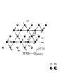
- Mn 3 is a diagram illustrating the direction of spin of localization of Sn. It is a state figure which shows the range which can be set as a magnetization free layer among the compounds of Mn and Ni. It is a graph of Hall resistance and magnetoresistance for Mn 3 Sn. It is a graph of Hall resistance at different temperatures for Mn 3 Sn. Mn 3 is a graph showing the relationship between the magnetic moment and the magnetic field for Sn.
- the memory element of the present invention constitutes a memory device capable of storing a large number of bits of data by being arranged in a matrix, for example. However, the description of the entire memory device is omitted here, and attention is paid to the memory element. Will be described below.
- the non-collinear antiferromagnet has a spin structure in which the magnetic moments (localized spin directions) of atoms on lattice points are inclined and non-parallel to each other.
- Non-collinear antiferromagnets include coplanar structures in which the magnetic moments in the spin structure are inclined in the same plane, and non-coplanar structures in which the direction of the magnetic moment is not in the same plane but is three-dimensionally inclined. There is a thing of sex. In any non-collinear antiferromagnetic material, the anomalous Hall effect appears when a current is passed due to the magnetic moments being inclined with respect to each other.
- an electron responsible for conduction that is, a conduction electron D
- a conduction electron D has a spin structure in which each magnetic moment M1 of an atom A on a lattice point is sterically inclined with respect to each other.
- the direction of the spin Da of the conduction electron D is directed to the direction of the magnetic moment M1 due to the influence of the magnetic moment M1. Since each magnetic moment M1 is inclined and non-parallel, the direction of the spin Da of the conduction electron D rotates when the conduction electron D goes around the nearest lattice point as shown on the right side of the figure. exercise.
- the rotational motion of the spin Da of the conduction electron D induces the rotational motion of the orbital motion of the conduction electron D.
- the rotating motion of the orbital motion of the conduction electrons D thus induced forms an electric field in a direction perpendicular to the current by being coupled with the current when an electric current is applied, and exhibits an anomalous Hall effect.
- the anomalous Hall effect is also manifested in the same principle for non-collinear antiferromagnetic materials having coplanarity.
- the direction of the electric field (positive or negative of the Hall voltage) generated by the abnormal Hall effect is determined by the rotation direction of the orbital motion of the spin Da.
- the rotational direction of the orbital motion of the spin Da is changed by reversing the direction of the magnetic moment M1.
- the inventors have found that the direction of the magnetic moment M1 can be reversed.
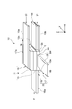
- the memory element 10 includes an element unit 20, and the write electrode unit 15, the read electrode unit 16, and the output electrode unit 17 are provided in the element unit 20. It has a configuration.
- the element unit 20 has a configuration in which a magnetization free layer (free layer) 12, a nonmagnetic layer 13, and a magnetization fixed layer (pinned layer) 14 formed in a film shape are sequentially stacked, and the magnetization direction of the magnetization free layer 12 Can change.
- Mn 3 Sn is hexagonal and has an a-axis between 50K and 430K with the a-axis ([2-1-10]) and b-axis ([-12-10]) as shown in FIG.
- a kagome lattice having a distortion in the distance between adjacent Mn is formed.
- the magnetic moment (localized spin direction) M2 of Mn (manganese) exists in the ab plane in a zero magnetic field, and geometric frustration appears as an inverted triangular spin structure.
- Mn 3 Sn constitutes a chiral spin structure having a vector chirality opposite to that of a normal 120 ° spin structure.
- Mn 3 Sn among the magnetic moments M2 of three adjacent Mn arranged in a triangle, one magnetic moment M2 is parallel to the easy axis of magnetization, but the other two magnetic moments M2 are inclined from the easy axis of magnetization.
- the magnetic moments M2 are inclined with respect to each other. In this way, in Mn 3 Sn which is a non-collinear antiferromagnetic material, the localized magnetic moments M2 are inclined to each other, and a small ferromagnetic moment is induced.
- a state in which the magnetic moment M2 of Mn in the magnetization free layer 12 is directed in a predetermined direction is defined as a first magnetization state.
- Data “1” is associated with the state.
- Mn 3 Sn forming the magnetization free layer 12 has a magnetic moment M2 of Mn of 2.78 ⁇ 10 ⁇ 23 A ⁇ m 2 (3 ⁇ B ) or less.
- the magnetic moments M2 of the three Mn atoms in the chiral spin structure cancel each other, but the magnetic moments are not partially canceled. That is, the weak magnetic moment of 2.78 ⁇ 10 ⁇ 26 JT ⁇ 1 / Mn (0.003 ⁇ B / Mn) or less remains due to the two magnetic moments M2 inclined to the local easy axis in the chiral spin structure.
- the magnetization free layer 12 is magnetized in the (magnetization direction).
- the magnetization free layer 12 formed by Mn 3 Sn becomes weakly magnetized, it is due to a very weak magnetic moment, so that the leakage magnetic field can be suppressed as compared with the conventional ferromagnet. .
- this Mn 3 Sn reverses the magnetic moment M2 of Mn in the first magnetization state as shown in FIG. 3 by, for example, a spin transfer torque (spin injection) method or a magnetic field application method, Further, it is possible to return the magnetic moment M2 from the inverted state to the first magnetization state. Thereby, it can be set as the 2nd magnetization state which the magnetic moment M2 changed to the direction different from a 1st magnetization state. Also in the second magnetization state, similarly to the first magnetization state, the magnetic moments M2 of the three Mn of the chiral spin structure cancel each other incompletely, leaving a weak magnetic moment, and the magnetization free layer 12 in that direction (magnetization direction).
- the magnetic moment M2 can be repeatedly changed between the first magnetization state and the second magnetization state.
- the rotation direction of the orbital motion of the spin Da of the conduction electron D of the magnetization free layer 12 is reversed. To do. Thereby, the direction of the electric field due to the anomalous Hall effect changes according to the magnetization direction.
- the memory element 10 includes a magnetization reversal unit 21 including, for example, a nonmagnetic layer 13, a magnetization fixed layer 14, and a write electrode unit 15.
- the magnetization direction of the magnetization free layer 12 is reversed by the spin transfer torque method.
- the first magnetization state of the magnetization free layer 12 is associated with data “1”
- the second magnetization state is associated with data “0”.
- Mn 3 Sn is used as the non-collinear antiferromagnetic material of the magnetization free layer 12, but other non-collinear hexagonal antiferromagnetic materials are used.
- the magnetization free layer 12 can be formed.
- non-collinear hexagonal antiferromagnetic materials include Mn 3 Ge and Mn 3 Ga.
- an antiferromagnetic material having non-coplanarity and capable of reversing the magnetization direction, that is, capable of reversing the magnetic moment of the chiral spin structure can be used as the magnetization free layer 12.
- antiferromagnetic materials include cubic substances and compounds.
- cubic alloys containing Mn or Fe of ⁇ phase (FCC (face-centered cubic) structure), for example, ⁇ - (Fe, Mn), Mn 3 Ir, Mn 3 Pt.
- ⁇ - (Fe, Mn), Mn 3 Ir, Mn 3 Pt cubic alloys containing Mn or Fe of ⁇ phase
- ⁇ - (Fe, Mn) cubic alloys containing Mn or Fe of ⁇ phase
- Mn face-centered cubic structure
- the memory element 10 associates 1-bit data “1” or “0” with the magnetization direction of the magnetization free layer 12 as described above, and the magnetization direction of the magnetization free layer 12 is reversed. The data is rewritten, and then the written data can be read out.
- the magnetization free layer 12 in the element portion 20, is formed of an antiferromagnetic material that exhibits an anomalous Hall effect and can reverse the magnetization direction. The generation of the leakage magnetic field can be suppressed more than the memory element using the.
- the direction along the stacking direction of the element unit 20 is defined as the Z direction, and the directions orthogonal to the Z direction and orthogonal to each other are defined as the X direction and the Y direction.
- a sign “+” is attached with the direction of the arrow shown in the figure as positive, and a sign “ ⁇ ” is attached with the reverse direction as negative.
- the magnetization free layer 12 is formed with a film thickness of, for example, about several nm to 100 nm.
- the Hall voltage V generated by the magnetization free layer 12 at the time of reading is lower as the film thickness of the magnetization free layer 12 is smaller. Since it becomes high, it is preferable to reduce the film thickness. Further, when the magnetization free layer 12 is formed, the ab plane includes the Z direction.
- the magnetization free layer 12 can be formed, for example, by sputtering using an antiferromagnetic material as a target, in this example, a polycrystalline Mn 3 Sn.
- the magnetization free layer 12 is formed so that the Z direction, that is, the direction in which the magnetization fixed layer 14 or the like is laminated is in the ab plane as described above, the c axis is in any direction in the xy plane. May be suitable.
- the magnetization free layer 12 is not limited to a single crystal but may be polycrystalline.
- the magnetization fixed layer 14 to be described later may have its c axis facing any direction in the xy plane as long as the Z direction is in the ab plane. Single crystal or polycrystal may be used.
- the magnetic field leakage of the magnetization free layer 12 is very weak (about 1/1000) as compared with the ferromagnetic material, and there is almost no leakage magnetic field from the magnetization free layer 12. For this reason, there is no interference due to the leakage magnetic field between the memory elements 10, and the structure is advantageous for increasing the degree of integration by increasing the density.
- the magnetization fixed layer 14 of the magnetization switching unit 21 is fixed in the same magnetization direction as the first magnetization state of the magnetization free layer 12.
- a ferromagnetic material such as permalloy, CoFeB, or FePt can be used as the magnetization fixed layer 14, but an antiferromagnetic material is preferably used from the viewpoint of the influence of the leakage magnetic field.
- the antiferromagnetic material used for the magnetization fixed layer 14 it is preferable to use an antiferromagnetic material whose magnetization direction is not easily reversed compared to the antiferromagnetic material of the magnetization free layer 12, for example, Mn 3 Sn used in the magnetization free layer 12.
- the magnetization fixed layer 14 can fix the magnetization direction by increasing its thickness, for example. Further, the magnetization direction of the magnetization fixed layer 14 may be stably fixed as a structure in which an antiferromagnetic layer such as IrMn or PtMn is laminated on the surface of the magnetization fixed layer 14 opposite to the nonmagnetic layer 13. .
- the nonmagnetic layer 13 is formed with a film thickness of, for example, about several nm.
- the nonmagnetic layer 13 may be an insulating film or a conductor film, but is preferably a conductor film from the viewpoint of suppressing heat generation and increasing efficiency when the magnetization direction of the magnetization free layer 12 is reversed.
- the write electrode portion 15 is composed of a pair of electrodes 15a and 15b, and one electrode 15a is connected to the upper surface of the magnetization fixed layer 14 (the surface opposite to the bonding surface with the nonmagnetic layer 13), and the magnetization Another electrode 15b is connected to the lower surface of the free layer 12 (the surface opposite to the bonding surface with the nonmagnetic layer 13), and these electrodes 15a and 15b are provided so as to sandwich the element portion 20.
- 15b is connected to a write control unit (not shown), and when data is rewritten, one of the write currents Ip1 and Ip2 is supplied by the write control unit.
- the write control unit supplies the write current Ip1 from the electrode 15b to the electrode 15a, for example.
- the spin-polarized electrons are incident on the magnetization free layer 12, and torque is applied to the spins of electrons in the magnetization free layer 12, so that the magnetization free layer 12 enters the first magnetization state.
- the write control unit applies the write current Ip2 from the electrode 15a to the electrode 15b. Supplied.
- the write current Ip2 As a result, electrons are conducted from the electrode 15 b to the magnetization free layer 12, but pass through the thin magnetization free layer 12 with little influence, and enter the magnetization fixed layer 14 through the nonmagnetic layer 13.
- electrons incident on the magnetization fixed layer 14 electrons that are spin-polarized in the direction corresponding to the first magnetization state pass through the magnetization fixed layer 14, but electrons that are spin-polarized in the opposite direction are fixed in magnetization.
- the write currents Ip1 and Ip2 for reversing the magnetization direction should be approximately the same as those of the ferromagnetic material. Is possible.
- the read electrode unit 16 and the output electrode unit 17 constitute a read unit 22 that reads the magnetization direction of the magnetization free layer 12.
- the read electrode portion 16 includes, for example, electrodes 16 a and 16 b whose longitudinal direction extends in the X direction, and these electrodes 16 a and 16 b are connected to the magnetization free layer 12. Of the side surfaces 12a and 12b facing in the X direction, one electrode 16a is connected to one side surface 12a and the other electrode 16b is connected to the other side surface 12b.
- a read control unit (not shown) is connected to the read electrode unit 16, and a read current If is supplied by the read control unit when data is read.
- the read electrode portion 16 is moved in the + X direction in the direction parallel to the film surface of the magnetization free layer 12 (the XY plane orthogonal to the X direction and the Y direction) (hereinafter referred to as the in-plane direction) by the electrodes 16a and 16b.
- a read current If is supplied.
- the output electrode portion 17 includes, for example, electrodes 17 a and 17 b whose longitudinal direction extends in the Y direction, and these electrodes 17 a and 17 b are connected to the magnetization free layer 12.
- one electrode 17a is connected to one side surface 12c of the side surfaces 12c and 12d facing in the Y direction, and another electrode 17b is connected to the other side surface 12d. .
- the output electrode unit 17 takes out the Hall voltage V generated in the Y direction perpendicular to the X direction in which the read current If flows in the in-plane direction in the magnetization free layer 12.
- the output electrode portion 17 includes the potential Va on the electrode 17a side connected to one side surface 12c of the magnetization free layer 12 and the potential on the electrode 17b side connected to the other side surface 12d of the magnetization free layer 12.
- the Hall voltage V is an electric signal corresponding to the magnetization direction of the magnetization free layer 12.
- the output electrode portion 17 outputs a positive or negative Hall voltage V due to the anomalous Hall effect generated in the magnetization free layer 12 through the electrodes 17a and 17b.
- data “1” or “0” is associated with positive / negative of the Hall voltage V in advance, and based on the positive / negative of the Hall voltage V obtained from the output electrode unit 17 during the data read operation. Data “1” or “0” can be discriminated.
- the direction of the Hall voltage V that is, the magnetization free layer 12 is generated by appropriately selecting the crystal structure and crystal axis direction of the antiferromagnetic material when forming the magnetization free layer 12 and the direction in which the read current If flows.
- the direction of the electric field due to the abnormal Hall effect can be set to a desired direction.
- the magnetization free is obtained only by providing the electrodes 16 a and 16 b for passing a current to the magnetization free layer 12 and the electrodes 17 a and 17 b for taking out the Hall voltage V of the magnetization free layer 12. Since the data can be read from the layer 12, the conventional MRAM does not require a reference memory element indicating a standard magnetoresistance value provided for determining the magnitude of the magnetoresistance, and the structure is simplified accordingly. And can be made smaller than before.
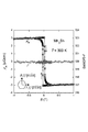
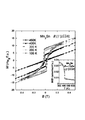
- Mn 3 Sn is a hysteresis in which the Hall resistivity ⁇ H changes in a width of about 6 ( ⁇ cm) (+3 ( ⁇ cm) to ⁇ 3 ( ⁇ cm)) with respect to the change of the applied magnetic field. was gotten. It was confirmed that the variation range of the Hall resistivity ⁇ H is extremely large as an antiferromagnetic material and larger than the variation range of the Hall resistivity found in transition metal ferromagnets such as iron, cobalt, and nickel. . Further, Hall resistivity [rho H of Mn 3 Sn is in the range of magnetic field of 0.03 T (300 gauss) or less, the Hall resistivity [rho H has changed. In this specification, in the notation of Miller index, “-” means a bar attached to the index immediately after that.
- Mn 3 Sn exhibits an anomalous Hall effect that exceeds that of a ferromagnetic material at a temperature in a normal use environment such as room temperature.
- the film thickness of Mn 3 Sn is 100 nm, it has been confirmed that the Hall resistivity ⁇ H due to the anomalous Hall effect is about 500 (m ⁇ ), and if the film thickness is about 5 nm, the Hall resistance is increased. It has been confirmed that the rate ⁇ H can be increased to about 1.0 ( ⁇ ). That is, it was found that Mn 3 Sn used for the magnetization free layer 12 can obtain a large voltage due to the sufficiently large abnormal Hall effect.
- the magnetic resistivity ⁇ is substantially constant except that it changes in a spike shape within the range of the magnetic field in which the Hall resistivity ⁇ H changes rapidly. Therefore, it is possible to easily know the magnitude of the anomalous Hall effect of Mn 3 Sn excluding the components of the normal Hall effect (also called normal Hall effect).
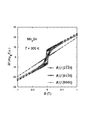
- Mn 3 Sn is extremely weak (4 to 7 (m ⁇ B / fu), but is reversed by a magnetic field of about 0.01 T (100 gauss) to 0.03 T (300 gauss). Therefore, it can be seen that Mn 3 Sn is not easily affected by an external magnetic field in the same manner as a ferromagnetic material.
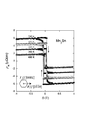
- Mn 3 Sn has an anomalous Hall effect up to 50K on the low temperature side. Further, from the relationship of the magnetic moment to magnetic field ratio (M / B) with respect to the temperature shown in FIG. 7, it was confirmed that the Neel temperature of Mn 3 Sn was 430K. Therefore, it was confirmed that the magnetic free layer 12 can be operated in the range of 50K to 430K. Further, as shown in FIG. 8, in 300K, to Mn 3 Sn, the case of applying the parallel magnetic field and [01-10], with respect to Mn 3 Sn as described above, the [2-l-l0] It was found that the magnetic moment of Mn 3 Sn is almost isotropic in the plane with respect to the magnetic moment of Mn 3 Sn. On the other hand, when a magnetic field was applied to Mn 3 Sn in parallel with its [0001] (c-axis), the magnetic moment was linearly changed at all temperatures measured between 100K and 450K. .
- the sample of Mn 3 Sn was prepared as follows. In addition, the following manufacturing methods are shown as preparation of a sample, and the method for manufacturing the magnetization free layer 12 is not limited.
- a plurality of polycrystalline samples were prepared by arc melting a mixture of Mn and Sn in a clean argon atmosphere. Mn was added in excess (10 mol%) exceeding the normal composition amount in consideration of loss during arc melting and crystal growth.
- the obtained polycrystalline material was used for crystal growth by the Czochralski method using a tetra-arc furnace.
- the Hall resistivity ⁇ H and the magnetic resistivity ⁇ were measured by a standard 4-probe method using a physical property measuring apparatus (PPMS, manufactured by Quantum Design).
- the magnetic moment was measured using a SQUID magnetization measuring device (MPMS, manufactured by Quantum Design).
- a write current Ip 1 in the + Z direction or a write current Ip 2 in the ⁇ Z direction is supplied from the write electrode unit 15 to the element unit 20 in accordance with the data to be written. For example, when the data is rewritten from “0” to “1”, the write current Ip1 flows from the electrode 15b to the electrode 15a via the element portion 20. As a result, the electrons conducted from the electrode 15 a to the magnetization fixed layer 14 are spin-polarized in the direction along the magnetization direction of the first magnetization state of the magnetization fixed layer 14 and enter the magnetization free layer 12.
- the spin-polarized electrons are incident on the magnetization free layer 12, so that the electrons exert a torque on the magnetization free layer 12, the magnetization direction of the magnetization free layer 12 is reversed, and magnetization free Layer 12 is in the first magnetization state. As a result, data “1” is written.
- the write control unit causes the write current Ip2 to flow from the electrode 15a to the electrode 15b via the element unit 20.
- electrons conducted from the electrode 15 b to the magnetization free layer 12 pass through the magnetization free layer 12 with almost no influence, and enter the magnetization fixed layer 14 through the nonmagnetic layer 13. Then, among the electrons incident on the magnetization fixed layer 14, electrons that are spin-polarized in the direction corresponding to the magnetization direction of the second magnetization state are reflected by the magnetization fixed layer 14 and reenter the magnetization free layer 12.
- the re-incident electrons exert a torque on the spins of the electrons in the magnetization free layer 12, thereby reversing the magnetization direction of the magnetization free layer 12 and causing the magnetization free layer 12 to enter the second magnetization state. As a result, data “0” is written.
- the magnetization free layer 12 holds the first or second magnetization state magnetized as described above. Even if another memory element 10 is arranged close to the memory element, there is almost no leakage magnetic field from the memory element 10, so that the magnetization direction of the magnetization free layer 12 is not changed and data is not lost.
- a read current If flows from the electrode 16a to the electrode 16b by the read control unit.
- the magnetization free layer 12 has a spin structure in which the localized spins are inclined with respect to each other. Rotational motion is induced, resulting in an anomalous Hall effect.
- the antiferromagnetic material of the magnetization free layer 12 can repeatedly reverse the magnetization direction. Therefore, data can be rewritten repeatedly, and of course, data can be repeatedly read.
- a memory element 30 according to the second embodiment is shown in FIG. 9 in which the same reference numerals are assigned to corresponding parts to those in FIG.
- the memory element 30 uses the spin Hall effect to generate a spin current by a current and control the magnetization direction of the antiferromagnetic material in the magnetization free layer 12.
- the memory element 30 includes a magnetization free layer 12, a reading unit 22 including a reading electrode unit 16 and an output electrode unit 17, and a magnetization switching unit 31.
- the memory element 30 according to the second embodiment differs from the memory element 10 (FIG. 2) according to the first embodiment described above in the configuration of the magnetization reversal unit 31, and an antiferromagnetic material of the magnetization free layer 12 is used. The inversion method is different.
- the magnetization free layer 12 is the same as that in the first embodiment described above, and is formed of a non-collinear antiferromagnetic material, which generates an anomalous Hall effect and allows the magnetization direction to be reversed. Yes. Further, since the configuration of the reading unit 22 and the reading procedure by the magnetization free layer 12 and the reading unit 22 are the same as those in the first embodiment, detailed description thereof will be omitted here.
- the spin Hall effect is caused by spin-orbit interaction in the non-magnetic material or semiconductor due to spin-up electrons and downward spins in a direction perpendicular to the current direction. Electrons are bent in opposite directions, and a spin current is generated in the normal direction of the plane formed by the direction of spin and the direction of current, resulting in spin accumulation at the edge of the nonmagnetic material or semiconductor.
- the magnetization reversal part 31 is composed of a spin Hall effect layer 32 and a write electrode part 33.
- the spin Hall effect layer 32 is formed in a film shape on the film surface of the magnetization free layer 12.
- the spin Hall effect layer 32 is formed of a nonmagnetic material having a large spin Hall effect, such as Pt (platinum) or Ta (tantalum).
- the write electrode portion 33 is composed of, for example, electrodes 33 a and 33 b whose longitudinal direction extends in the X direction, and these electrodes 33 a and 33 b are connected to the spin Hall effect layer 32. Among the side surfaces facing in the X direction, one electrode 33a is connected to the spin Hall effect layer 32 in the X direction, and the other electrode 33b is connected to the other side surface. As a result, the write electrode unit 33 supplies write currents Ip1 and Ip2 to the spin Hall effect layer 32 in the X direction.
- the write current Ip1 is a current flowing in the ⁇ X direction
- the write current Ip2 is a current flowing in the + X direction opposite to the write current Ip1.
- the write electrode unit 33 causes the spin hole to be changed.
- a write current Ip 1 is passed through the effect layer 32, and electrons are passed in the + X direction in the spin Hall effect layer 32.
- the electrons are bent in a direction perpendicular to the direction of spin and the direction of electron flow by the spin Hall effect.
- electrons with upward (+ Y direction) spin are bent in the + Z direction
- electrons with downward spin are bent in the ⁇ Z direction.
- the write electrode unit 33 causes the spin hole to be changed.
- a write current Ip2 is supplied to the effect layer 32, and electrons are supplied in the ⁇ X direction in the spin Hall effect layer 32.
- the electrons are bent in a direction perpendicular to the direction of spin and the direction of electron flow by the spin Hall effect. Thereby, for example, electrons with upward (+ Y direction) spin are bent in the ⁇ Z direction, and electrons with downward spin ( ⁇ Y direction) are bent in the + Z direction.
- the upward spin electrons flow from the spin Hall effect layer 32 into the magnetization free layer 12 and exert a torque on the magnetization of the magnetization free layer 12.
- the magnetization free layer 12 is magnetized to the second magnetization state by reversing the magnetization direction of the antiferromagnetic material in the first magnetization state.
- the memory element 30 according to the second embodiment also uses the antiferromagnetic material that exhibits the anomalous Hall effect and whose magnetization direction can be reversed, and the magnetization free layer whose magnetization direction is reversed according to data. 12 can significantly suppress the leakage magnetic field as compared with a conventional memory element using a ferromagnetic material, and can reduce the influence of the leakage magnetic field on other adjacent memory elements when highly integrated. Thus, the leakage magnetic field is small and high integration can be achieved.
- the spin Hall effect layer 32 and the write electrode portion 33 for writing data, and the magnetization pinned layer provided in the conventional MRAM is not necessary, and the structure can be simplified correspondingly. Therefore, the size can be reduced as compared with the prior art.
- a memory element 40 according to the third embodiment is shown in FIG. 10 in which the same reference numerals are assigned to the parts corresponding to FIG.
- the memory element 40 controls the magnetization direction of the antiferromagnetic material in the magnetization free layer 12 using the anomalous Hall effect.
- the memory element 40 includes a magnetization free layer 12, a reading unit 22 including a reading electrode unit 16 and an output electrode unit 17, and a magnetization switching unit 41.
- the memory element 40 according to the third embodiment is different from the memory element 10 according to the first embodiment in the configuration of the magnetization switching unit 41 and in the method for inverting the antiferromagnetic material of the magnetization free layer 12. .
- the magnetization free layer 12 is the same as that in the first embodiment described above, and is formed of a non-collinear antiferromagnetic material, which generates an anomalous Hall effect and allows the magnetization direction to be reversed. Yes. Further, since the configuration of the reading unit 22 and the reading procedure by the magnetization free layer 12 and the reading unit 22 are the same as those in the first embodiment, detailed description thereof will be omitted here.
- the magnetization switching unit 41 includes a magnetization fixed layer 42, a nonmagnetic layer 43, and a write electrode unit 44.
- the nonmagnetic layer 43 is formed on the film surface of the magnetization free layer 12 and is disposed so as to be sandwiched between the magnetization free layer 12 and the magnetization fixed layer 42.
- the magnetization fixed layer 42 is a ferromagnet or antiferromagnet having a large anomalous Hall effect. Examples of the ferromagnetic material having a large anomalous Hall effect include NiFe, CoFeB, and FePt. Examples of the antiferromagnetic material having a large anomalous Hall effect include Mn 3 Sn, Mn 3 Ge, Mn 3 Ga, Mn 3 Ir, and Mn 3 Pt.
- the magnetization fixed layer 42 is formed of a ferromagnetic material
- the magnetization direction is fixed in a predetermined direction.
- the magnetization fixed layer 42 is formed of an antiferromagnetic material
- the configuration is as follows.
- the nonmagnetic layer 43 is formed, for example, to a thickness of about several nanometers, and may be an insulating film or a conductor film similarly to the nonmagnetic layer 13 of the first embodiment.
- the write electrode section 44 is composed of, for example, electrodes 44 a and 44 b whose longitudinal direction extends in the X direction, and these electrodes 44 a and 44 b are connected to the magnetization fixed layer 42. Of the side surfaces facing each other in the X direction, one electrode 44a is connected to the magnetization fixed 42, and the other electrode 44b is connected to the other side surface. As a result, the write electrode unit 44 causes the write currents Ip1 and Ip2 to flow in the X direction with respect to the fixed magnetization layer 42.
- the write current Ip1 is a current flowing in the ⁇ X direction
- the write current Ip2 is a current flowing in the + X direction opposite to the write current Ip1.
- the write current Ip1 in the magnetization fixed layer 42 is changed.
- a spin-polarized current spin current with current
- the spin of electrons in a predetermined direction exerts a torque on the magnetization of the antiferromagnetic material in the magnetization free layer 12, and the magnetization free layer 12 has the magnetization direction of the antiferromagnet in the second magnetization state in the first magnetization state. Is magnetized.
- the write current Ip 2 is supplied to the magnetization fixed layer 42.
- a spin-polarized current is generated in the Z direction by the anomalous Hall effect.
- the spin of electrons in the direction opposite to that when the write current Ip1 is applied exerts a torque on the magnetization of the antiferromagnetic material in the magnetization free layer 12, and the magnetization free layer 12 is in the first magnetization state. Is magnetized to the second magnetization state.
- the magnetization fixed layer 42 may have a structure in which an antiferromagnetic layer is laminated on the surface of the ferromagnetic material opposite to the nonmagnetic layer 43, similarly to the magnetization fixed layer 14 of the first embodiment.
- an antiferromagnetic material as the magnetization fixed layer 14 rather than a ferromagnetic material from the viewpoint of the influence of the leakage magnetic field.
- the memory element 40 according to the third embodiment also uses the antiferromagnetic material that exhibits the anomalous Hall effect and whose magnetization direction can be reversed, and the magnetization free layer whose magnetization direction is reversed according to data. 12 can significantly suppress the leakage magnetic field as compared with a conventional memory element using a ferromagnetic material, and can reduce the influence of the leakage magnetic field on other adjacent memory elements when highly integrated. Thus, the leakage magnetic field is small and high integration can be achieved.
- a memory element 50 according to the fourth embodiment is shown in FIG. 11 in which the same reference numerals are assigned to the parts corresponding to FIG.
- the memory element 50 controls the magnetization direction of the antiferromagnetic material in the magnetization free layer 12 by applying a magnetic field.
- the memory element 50 includes a magnetization free layer 12, a reading unit 22 including a reading electrode unit 16 and an output electrode unit 17, and a magnetization switching unit 51.
- the memory element 50 according to the fourth embodiment is different from the memory element 10 according to the first embodiment described above in the configuration of the magnetization reversal unit 51 and the method for inverting the antiferromagnetic material of the magnetization free layer 12 is different. ing.
- the magnetization free layer 12 is the same as that in the first embodiment described above, and is formed of a non-collinear antiferromagnetic material, which generates an anomalous Hall effect and allows the magnetization direction to be reversed. Yes. Further, since the configuration of the reading unit 22 and the reading procedure by the magnetization free layer 12 and the reading unit 22 are the same as those in the first embodiment described above, detailed description thereof is omitted here.
- the magnetization reversal unit 51 includes a word line 52 and a bit line 53.
- the word line 52 has a longitudinal direction extending in the Y direction
- the bit line 53 has a longitudinal direction extending in the X direction, for example.
- the magnetization free layer 12 is provided at a position where the word line 52 and the bit line 53 intersect with each other, and is disposed so as to be sandwiched between the word line 52 and the bit line 53 in the Z direction.
- a write current Iw is supplied to the word line 52 in the + Y direction by a write control unit (not shown).
- one of the write currents Ib1 and Ib2 is passed through the bit line 53 by a write control unit (not shown). Of the currents flowing through the bit line 53, one write current Ib1 flows in the + X direction, and among the currents flowing through the bit line 53, the other write current Ib2 flows in the -X direction.
- the write current Iw is applied to the word line 52.
- the write current Ib1 is supplied to the bit line 53.
- the write current Iw is applied to the word line 52.
- the write current Ib2 is supplied to the bit line 53.
- a combined magnetic field of a magnetic field generated by the write current Iw flowing and a magnetic field generated by the write current Ib2 flowing is applied to the magnetization free layer 12.
- the memory element 50 according to the fourth embodiment also uses the antiferromagnetic material that exhibits the anomalous Hall effect and whose magnetization direction can be reversed, and the magnetization free layer whose magnetization direction is reversed according to data. 12 can significantly suppress the leakage magnetic field as compared with a conventional memory element using a ferromagnetic material, and can reduce the influence of the leakage magnetic field on other adjacent memory elements when highly integrated. Thus, the leakage magnetic field is small and high integration can be achieved.
- the memory element 50 uses a non-collinear antiferromagnetic material as the magnetization free layer 12, the magnetic field is comparable to that of a conventional memory element using a magnetization free layer made of a ferromagnetic material.
- the magnetization direction of the magnetization free layer 12 can be reversed.
- a magnetic field of 0.01 to 0.1 T 100 to 1000 gauss is required to reverse the magnetization direction of the magnetization free layer.
- the magnetization direction of the magnetization free layer 12 is reversed by applying a magnetic field of about 0.01T to 0.03T (100 to 300 gauss). be able to.
- a plurality of word lines 52 are arranged in the X direction, and a plurality of bit lines 53 are arranged in the Y direction so that the word lines 52 and the bit lines 53 are arranged.
- the magnetization free layer 12 is provided at each intersecting position.
- the word line 52 and the bit line 53 that intersect at the position of the magnetization free layer 12 whose magnetization is to be reversed are selected, and the write current Iw and the write current Ib1 or Ib2 are passed as described above.
- a non-collinear antiferromagnetic material is used as the material for forming the magnetization free layer.
- the antiferromagnetic material exhibits an anomalous Hall effect and the magnetization direction can be reversed.
- the magnetization free layer may be formed using an antiferromagnetic material other than the non-collinear antiferromagnetic material.
- a memory element 60 according to the fifth embodiment is shown in FIG.
- the magnetization direction (that is, data) of the antiferromagnetic material in the magnetization free layer 12 is read based on the change in electrical resistance due to the magnetoresistance effect.
- the magnetoresistive effect includes a tunnel magnetoresistive effect and a giant magnetoresistive effect. In this example, the tunnel magnetoresistive effect is used.
- the memory element 60 of the fifth embodiment is different from the memory element 10 of the first embodiment described above in the configuration of the magnetization switching unit 71 and the reading unit 72, and the antiferromagnetic material of the magnetization free layer 12 is used. The inversion method and the data reading method are different.
- the memory element 60 includes an element unit 70, a magnetization reversing unit 71, and a reading unit 72.
- the element unit 70 has a configuration in which the magnetization free layer 12, the nonmagnetic layer 13, and the magnetization fixed layer 14 are stacked.
- the magnetization free layer 12 is formed of an antiferromagnetic material whose magnetization direction can be reversed, as in the first embodiment described above, but does not need to be an antiferromagnetic material that exhibits an anomalous Hall effect.
- the nonmagnetic layer 13 and the magnetization fixed layer 14 are provided in order for the memory element 60 to function as a magnetic tunnel junction element. For this reason, the nonmagnetic layer 13 is formed of an insulator.
- the magnetization fixed layer 14 is the same as that of the first embodiment, and is formed of an antiferromagnetic material or a ferromagnetic material whose magnetization direction is fixed, for example, in a first magnetization state.
- the magnetization free layer 12 and the magnetization fixed layer 14 may be single crystal or polycrystalline. Further, the orientation of each crystal axis in the magnetization free layer 12 and the magnetization fixed layer 14 is not particularly limited as in the first embodiment.
- the memory element 60 functions as a magnetic tunnel junction element using the tunnel magnetoresistive effect, but the memory element 60 functions as a GMR (Giant Magneto Resistive) element using the giant magnetoresistive effect. You can also.
- the nonmagnetic layer 13 is formed of a metal (conductor).
- the magnetization reversal unit 71 includes a word line 74 and a bit line 75 that is disposed to face the word line 74 at a predetermined distance.
- the word line 74 has a longitudinal direction extending in the Y direction
- the bit line 75 has a longitudinal direction extending in the X direction orthogonal to the Y direction.
- the element unit 70 is provided at a position where the word line 74 and the bit line 75 intersect with each other, and is disposed between the word line 74 and the bit line 75 which are disposed to face each other in the Z direction orthogonal to the X direction and the Y direction. It is arranged to be sandwiched.
- the word line 74 and the bit line 75 are the same as the word line 52 and the bit line 53 (FIG.
- a write control unit (not shown) causes a write current Iw to flow in the + Y direction through the word line 74 and one of the write currents Ib1 and Ib2 to flow through the bit line 75.
- one write current Ib1 flowing through the bit line 75 flows in the + X direction
- the other write current Ib2 flows in the ⁇ X direction opposite to the one write current Ib1.
- the read unit 72 includes the bit line 75 and the read electrode 77.
- the bit line 75 also functions as the electrode of the magnetization switching unit 71 as described above. Therefore, the bit line 75 is a part of the configuration that forms the magnetization reversal unit 71 and also a part of the configuration that also functions as a read electrode of the read unit 72 to form the read unit 72. It is included in the configuration of both the magnetization switching unit 71 and the reading unit 72. Of course, an electrode different from the bit line 75 that also functions as the electrode of the magnetization reversal unit 71 may be provided together with the read electrode 77 as a reading electrode of the reading unit 72.
- a read electrode 77 is fixed on the surface opposite to the surface on which the nonmagnetic layer 13 is provided.
- the magnetization free layer 12 of the element unit 70 is provided with a plug (wiring) 78 on the surface opposite to the surface on which the nonmagnetic layer 13 is provided, and the bit line 75 is fixed to the plug 78.
- the read electrode 77 is electrically connected to the element portion 70
- the bit line 75 is electrically connected to the element portion 70 via the plug 78.
- the word line 74 is disposed on the lower side of the read electrode 77 so as to be opposed to the read electrode 77 at a predetermined distance.
- the bit line 75 and the read electrode 77 serving as read electrodes are connected to a read control unit (not shown).
- a transistor 79 is provided between the read electrode 77 and the read control unit.
- the read control unit turns on the transistor 79 and applies a predetermined voltage to the element unit 70 between the bit line 75 and the read electrode 77.
- Read control unit by the application of this voltage, supplying a read current I R to the bit line 75 from the reading electrode 77 through the device 70.
- Read current I R flowing through the element 70 when a predetermined voltage is applied varies with the electrical resistance of the magnitude of the element portion 70 caused by the magnetoresistance effect.
- Read control unit to determine the magnitude of the read current I R that corresponds to the electrical resistance of the element 70 caused by the magnetoresistance effect, determines the data "1" or "0".
- the electrical signal read current I R is according to the magnetization direction of the magnetization free layer 12.
- the data write procedure is the same as that of the memory element 50 of the fourth embodiment. That is, for example, when the magnetization free layer 12 is changed to the first magnetization state corresponding to the data “1”, the write current Iw is supplied to the word line 74 and the write current Ib1 is supplied to the bit line 75. As a result, in the element unit 70 arranged at the position where the word line 74 and the bit line 75 intersect, a combined magnetic field generated by the orthogonal write current Iw and write current Ib1 is applied to the magnetization free layer 12 and the magnetization The magnetization direction of the free layer 12 is reversed and changes from the second magnetization state to the first magnetization state.
- the write current Iw is supplied to the word line 74 and is directed in the direction opposite to the one write current Ib1.
- Another write current Ib2 is passed through the bit line 75.
- the read control unit When reading data, the read control unit turns on the transistor 79 and applies a predetermined voltage to the element unit 70 via the read electrode 77 and the bit line 75. That is, a voltage is applied to the element unit 70 perpendicularly to the junction surface of the magnetization free layer 12 and the nonmagnetic layer 13 and the junction surface of the nonmagnetic layer 13 and the magnetization fixed layer 14. By the application of this voltage, the element unit 70, the read current I R flows through the magnetization free layer 12 through the non-magnetic layer 13 from the magnetization fixed layer 14. When the magnetization directions of the magnetization free layer 12 and the magnetization fixed layer 14 are the same, the smaller the electric resistance of the element portion 70 by the tunnel magneto-resistance effect, draw large read current I R in the element unit 70.
- the electric resistance in the element unit 70 causes the magnetization directions of the magnetization free layer 12 and the magnetization fixed layer 14 to be different. It becomes larger than when the same flows a small read current I R than the read current I R flowing through the element 70 when the magnetization direction of the magnetization free layer 12 and the magnetization fixed layer 14 are the same.
- the read control unit determines "1" or "0" of the data stored in the memory device 60 based on the magnitude of the read current I R flowing through the element portion 70.
- the magnetization direction of the magnetization free layer 12 can be reversed by applying a magnetic field of about 0.01 T (100 gauss) to the magnetization free layer 12.
- the element unit 70 confirm that the magnetization to determine the magnetization direction of the magnetization free layer 12 relative to the fixed layer 14, does not change the magnetization direction of the magnetization free layer 12 is read current I R of about 1 ⁇ 5 mA flows is doing.
- the magnetization free layer 12 whose magnetization direction is reversed according to data is formed using an antiferromagnetic material whose magnetization direction is reversible.
- the leakage magnetic field can be remarkably suppressed as compared with the conventional memory element using a magnetic material, and when it is highly integrated, the influence of the leakage magnetic field on other adjacent memory elements can be reduced, and thus the leakage magnetic field is small. High integration can be achieved.
- the magnetization direction of the magnetization free layer 12 when writing data, the magnetization direction of the magnetization free layer 12 is reversed by applying a magnetic field to the magnetization free layer 12, but the configuration for writing data is not limited to this.
- the magnetization direction of the magnetization free layer 12 can be reversed by the spin transfer torque method.
- either one of the write currents Ip1 and Ip2 having different directions in the Z direction may be passed in accordance with the data to be written so as to penetrate the element unit 70.
- the magnetization direction of the magnetization free layer 12 can be reversed using the spin Hall effect.
- a spin Hall effect layer is provided on the surface of the magnetization free layer 12 opposite to the nonmagnetic layer 13, and either one of the write currents Ip1 and Ip2 having different directions in the X direction is provided on the spin Hall effect layer.
- a spin-polarized current may be used as in the third embodiment.
- a ferromagnetic material or an antiferromagnetic material having a large anomalous Hall effect is used as the magnetization fixed layer 14 of the element unit 70, and write currents Ip1 and Ip2 having different directions in the X direction are applied to the magnetization fixed layer 14. Either one of them is sent according to the data to be written.
- the read control unit determines the data "1” or “0” in the magnitude of the read current I R
- the read control unit supplies a constant current to the element unit 70 via the bit line 75 and the read electrode 77, and a voltage drop generated in the element unit 70 at that time, that is, the bit line 75 and the read electrode 77.
- the data “1” or “0” is determined by determining the magnitude of the potential difference between the two.
- the magnitude of the voltage drop can be determined as the magnitude of the voltage applied to the element unit 70.
- the magnetization free layer 12 is an antiferromagnetic material, but at least one of the magnetization free layer 12 and the magnetization fixed layer 14 may be an antiferromagnetic material. This is a preferred embodiment.
- the magnetization fixed layer 14 is used to reverse the magnetization direction of the magnetization free layer 12 in accordance with the data to be written.
- the magnetization free layer is read when data is read.
- the magnetization fixed layer 14 is used to extract an electric signal corresponding to the magnetization direction of 12.
- the magnetization fixed layer 14 changes the magnetization direction of the magnetization free layer 12 according to the data to be written. In addition to being inverted, it is used to take out an electrical signal corresponding to the magnetization direction of the magnetization free layer 12 when reading data.
- an antiferromagnetic material may be used as the magnetization fixed layer 14 and, for example, a ferromagnetic material may be used for the magnetization free layer 12. In this case, the other configurations may be the same.
- the antiferromagnetic material can be used for the magnetization free layer 12 and the magnetization fixed layer 14 as described above.
- an antiferromagnetic material is used for at least one of the magnetization free layer 12 and the magnetization fixed layer 14, a leakage magnetic field can be suppressed as compared with a configuration using a ferromagnetic material for both of them. Therefore, even in this case, the influence of the leakage magnetic field on other adjacent memory elements when highly integrated can be reduced, and thus the leakage magnetic field is small and high integration can be achieved.
- the Mn 3 Sn has a different six magnetization directions depending on the combination of directions of magnetic moments M2 of three adjacent Mn arranged in a triangle. Presumed to change. Therefore, in the first to fourth embodiments using the anomalous Hall effect of the magnetization free layer 12, the reversal of the magnetization direction between the first magnetization state and the second magnetization state is that the magnetization direction is necessarily rotated by 180 degrees.
- the magnetization direction in the first magnetization state may change to the second magnetization state rotated by a predetermined angle other than 180 degrees. Also in the fifth embodiment, if the electrical resistance due to the magnetoresistive effect changes, the reversal of the magnetization direction between the first magnetization state and the second magnetization state does not necessarily have to be rotated 180 degrees.
- the state of the magnetic moment M2 of Mn in the magnetization free layer 12 shown in FIG. 3 is set as the first magnetization state, and the magnetic moment M2 is reversed from the first magnetization direction (180
- the magnetization direction may not be specified. The same applies when the antiferromagnetic material other than Mn3Sn is the magnetization free layer 12.
- the electrodes constituting the write electrode portions 15, 33, 44 of the magnetization reversal portions 21, 31, 41, the read electrode portion 16, the output electrode portion 17, and the read portion 72 in each of the above embodiments are members that extract voltage. As long as it is a member for applying a voltage or a member for supplying a current, a member having another function may be used. For example, when a part of another element is directly connected to the magnetization free layer and a voltage is applied, a part of the other element becomes an electrode.
Landscapes
- Engineering & Computer Science (AREA)
- Computer Hardware Design (AREA)
- Chemical & Material Sciences (AREA)
- Power Engineering (AREA)
- Crystallography & Structural Chemistry (AREA)
- Materials Engineering (AREA)
- Hall/Mr Elements (AREA)
- Mram Or Spin Memory Techniques (AREA)
- Thin Magnetic Films (AREA)
Abstract
Priority Applications (2)
| Application Number | Priority Date | Filing Date | Title |
|---|---|---|---|
| JP2017530866A JP6888783B2 (ja) | 2015-07-24 | 2016-07-25 | メモリ素子 |
| US15/743,149 US10490247B2 (en) | 2015-07-24 | 2016-07-25 | Memory element |
Applications Claiming Priority (4)
| Application Number | Priority Date | Filing Date | Title |
|---|---|---|---|
| JP2015147092 | 2015-07-24 | ||
| JP2015-147092 | 2015-07-24 | ||
| JP2015211274 | 2015-10-27 | ||
| JP2015-211274 | 2015-10-27 |
Publications (1)
| Publication Number | Publication Date |
|---|---|
| WO2017018391A1 true WO2017018391A1 (fr) | 2017-02-02 |
Family
ID=57884380
Family Applications (1)
| Application Number | Title | Priority Date | Filing Date |
|---|---|---|---|
| PCT/JP2016/071778 Ceased WO2017018391A1 (fr) | 2015-07-24 | 2016-07-25 | Élément de mémoire |
Country Status (3)
| Country | Link |
|---|---|
| US (1) | US10490247B2 (fr) |
| JP (1) | JP6888783B2 (fr) |
| WO (1) | WO2017018391A1 (fr) |
Cited By (17)
| Publication number | Priority date | Publication date | Assignee | Title |
|---|---|---|---|---|
| JP6256965B1 (ja) * | 2017-03-29 | 2018-01-10 | 国立大学法人東北大学 | 記憶素子及び記憶素子の駆動方法 |
| WO2019163641A1 (fr) * | 2018-02-22 | 2019-08-29 | 株式会社アルバック | Procédé de formation d'un film magnétique et procédé de production d'un élément de stockage magnétique |
| JP2020017662A (ja) * | 2018-07-26 | 2020-01-30 | 株式会社アルバック | 磁気記憶素子、および、磁気記憶素子の製造方法 |
| JP2020065006A (ja) * | 2018-10-18 | 2020-04-23 | 株式会社アルバック | 磁気記憶素子の製造方法 |
| WO2020166722A1 (fr) * | 2019-02-15 | 2020-08-20 | 国立大学法人東京大学 | Élément spintronique et dispositif de mémoire magnétique |
| JPWO2020050329A1 (ja) * | 2018-09-05 | 2021-08-30 | 学校法人慶應義塾 | スピントロニクスデバイス、磁気メモリ及び電子機器 |
| KR20210116704A (ko) * | 2019-02-15 | 2021-09-27 | 어플라이드 머티어리얼스, 인코포레이티드 | 자기 메모리 디바이스들 및 형성 방법들 |
| US11411171B2 (en) | 2018-08-07 | 2022-08-09 | Ip2Ipo Innovations Limited | Non-volatile memory cell |
| JPWO2022220251A1 (fr) * | 2021-04-12 | 2022-10-20 | ||
| WO2022224500A1 (fr) * | 2021-04-21 | 2022-10-27 | 国立大学法人東北大学 | Dispositif numérique, son procédé de production et son procédé d'utilisation |
| WO2023234269A1 (fr) * | 2022-05-30 | 2023-12-07 | 国立大学法人東京大学 | Élément de mémoire magnétique, système de traitement d'informations et procédé de commande d'élément de mémoire magnétique |
| WO2024090370A1 (fr) * | 2022-10-28 | 2024-05-02 | 国立研究開発法人理化学研究所 | Élément de déplacement de paroi de domaine magnétique, dispositif de mémoire, et procédé d'écriture de données |
| WO2024150833A1 (fr) * | 2023-01-13 | 2024-07-18 | 国立大学法人東京大学 | Élément à effet magnétorésistif et dispositif de mémoire magnétique |
| WO2025009492A1 (fr) * | 2023-07-05 | 2025-01-09 | Jsr株式会社 | Procédé de fabrication d'élément de stockage magnétique |
| WO2025028421A1 (fr) * | 2023-07-28 | 2025-02-06 | Jsr株式会社 | Matériau de corps antiferromagnétique, film à deux couches de corps magnétique et d'isolant, élément magnétorésistif à effet tunnel et mémoire magnétique |
| WO2025079734A1 (fr) * | 2023-10-13 | 2025-04-17 | TopoLogic株式会社 | Élément de mémoire magnétique |
| WO2025211391A1 (fr) * | 2024-04-02 | 2025-10-09 | TopoLogic株式会社 | Dispositif de stockage à semi-conducteur et procédé de fabrication de dispositif de stockage à semi-conducteur |
Families Citing this family (8)
| Publication number | Priority date | Publication date | Assignee | Title |
|---|---|---|---|---|
| KR101868267B1 (ko) * | 2017-01-26 | 2018-06-15 | 고려대학교 산학협력단 | 고조파 홀 전압 분석 방법 |
| US10891999B1 (en) * | 2019-06-19 | 2021-01-12 | Western Digital Technologies, Inc. | Perpendicular SOT MRAM |
| KR102788422B1 (ko) | 2020-05-25 | 2025-04-01 | 삼성전자주식회사 | 자기 기억 소자 |
| JP7560871B2 (ja) * | 2021-02-03 | 2024-10-03 | 国立研究開発法人理化学研究所 | インダクター素子およびそれを含む機器 |
| CN113237834B (zh) * | 2021-07-08 | 2021-09-14 | 成都信息工程大学 | 基于光自旋霍尔效应的手性分子手性分辨装置及方法 |
| CN113851580A (zh) * | 2021-09-18 | 2021-12-28 | 中国科学院半导体研究所 | 自旋过滤磁隧道结、制备方法及设备 |
| CN113571632B (zh) * | 2021-09-23 | 2021-12-10 | 南开大学 | 一种反常霍尔元件及其制备方法 |
| CN115884601B (zh) * | 2022-11-28 | 2025-11-28 | 青岛海存微电子有限公司 | 磁存储器及其制造方法 |
Citations (9)
| Publication number | Priority date | Publication date | Assignee | Title |
|---|---|---|---|---|
| JP2001084756A (ja) * | 1999-09-17 | 2001-03-30 | Sony Corp | 磁化駆動方法、磁気機能素子および磁気装置 |
| JP2003069107A (ja) * | 2001-08-24 | 2003-03-07 | Hitachi Ltd | 磁界センサー及び磁気ヘッド |
| JP2007329492A (ja) * | 1999-09-16 | 2007-12-20 | Toshiba Corp | 磁気記録素子への書き込み方法および磁気記録素子 |
| WO2009133744A1 (fr) * | 2008-04-28 | 2009-11-05 | 日本電気株式会社 | Elément de stockage magnétique et mémoire magnétique |
| JP2010045387A (ja) * | 2009-10-14 | 2010-02-25 | Toshiba Corp | スピンメモリ |
| JP2010263221A (ja) * | 2009-05-08 | 2010-11-18 | Crocus Technology Sa | 低書き込み電流を用いる熱支援スピン移動トルク書き込み手順を備えた磁気メモリ |
| JP2012156376A (ja) * | 2011-01-27 | 2012-08-16 | Renesas Electronics Corp | 半導体装置 |
| JP2013069865A (ja) * | 2011-09-22 | 2013-04-18 | Toshiba Corp | 磁気メモリ |
| JP2014045196A (ja) * | 2012-08-26 | 2014-03-13 | Samsung Electronics Co Ltd | スイッチングに基づいたスピン軌道相互作用を使用する磁気トンネルリング接合と、磁気トンネルリング接合を利用するメモリを提供するための方法及びシステム |
Family Cites Families (8)
| Publication number | Priority date | Publication date | Assignee | Title |
|---|---|---|---|---|
| US6611405B1 (en) | 1999-09-16 | 2003-08-26 | Kabushiki Kaisha Toshiba | Magnetoresistive element and magnetic memory device |
| US7489541B2 (en) * | 2005-08-23 | 2009-02-10 | Grandis, Inc. | Spin-transfer switching magnetic elements using ferrimagnets and magnetic memories using the magnetic elements |
| US7643332B2 (en) * | 2006-06-23 | 2010-01-05 | Infineon Technologies Ag | MRAM cell using multiple axes magnetization and method of operation |
| US8004881B2 (en) * | 2007-12-19 | 2011-08-23 | Qualcomm Incorporated | Magnetic tunnel junction device with separate read and write paths |
| FR2925747B1 (fr) * | 2007-12-21 | 2010-04-09 | Commissariat Energie Atomique | Memoire magnetique a ecriture assistee thermiquement |
| JP2009158789A (ja) * | 2007-12-27 | 2009-07-16 | Hitachi Global Storage Technologies Netherlands Bv | 電流磁気効果素子及び磁気センサ |
| US7965543B2 (en) * | 2009-04-30 | 2011-06-21 | Everspin Technologies, Inc. | Method for reducing current density in a magnetoelectronic device |
| US8824200B1 (en) * | 2013-12-17 | 2014-09-02 | The United States Of America As Represented By The Secretary Of The Army | Nonvolative memory cells programable by phase change |
-
2016
- 2016-07-25 WO PCT/JP2016/071778 patent/WO2017018391A1/fr not_active Ceased
- 2016-07-25 JP JP2017530866A patent/JP6888783B2/ja active Active
- 2016-07-25 US US15/743,149 patent/US10490247B2/en active Active
Patent Citations (9)
| Publication number | Priority date | Publication date | Assignee | Title |
|---|---|---|---|---|
| JP2007329492A (ja) * | 1999-09-16 | 2007-12-20 | Toshiba Corp | 磁気記録素子への書き込み方法および磁気記録素子 |
| JP2001084756A (ja) * | 1999-09-17 | 2001-03-30 | Sony Corp | 磁化駆動方法、磁気機能素子および磁気装置 |
| JP2003069107A (ja) * | 2001-08-24 | 2003-03-07 | Hitachi Ltd | 磁界センサー及び磁気ヘッド |
| WO2009133744A1 (fr) * | 2008-04-28 | 2009-11-05 | 日本電気株式会社 | Elément de stockage magnétique et mémoire magnétique |
| JP2010263221A (ja) * | 2009-05-08 | 2010-11-18 | Crocus Technology Sa | 低書き込み電流を用いる熱支援スピン移動トルク書き込み手順を備えた磁気メモリ |
| JP2010045387A (ja) * | 2009-10-14 | 2010-02-25 | Toshiba Corp | スピンメモリ |
| JP2012156376A (ja) * | 2011-01-27 | 2012-08-16 | Renesas Electronics Corp | 半導体装置 |
| JP2013069865A (ja) * | 2011-09-22 | 2013-04-18 | Toshiba Corp | 磁気メモリ |
| JP2014045196A (ja) * | 2012-08-26 | 2014-03-13 | Samsung Electronics Co Ltd | スイッチングに基づいたスピン軌道相互作用を使用する磁気トンネルリング接合と、磁気トンネルリング接合を利用するメモリを提供するための方法及びシステム |
Cited By (40)
| Publication number | Priority date | Publication date | Assignee | Title |
|---|---|---|---|---|
| WO2018179193A1 (fr) * | 2017-03-29 | 2018-10-04 | 国立大学法人東北大学 | Élément de mémoire et procédé de commande d'élément de mémoire |
| JP6256965B1 (ja) * | 2017-03-29 | 2018-01-10 | 国立大学法人東北大学 | 記憶素子及び記憶素子の駆動方法 |
| WO2019163641A1 (fr) * | 2018-02-22 | 2019-08-29 | 株式会社アルバック | Procédé de formation d'un film magnétique et procédé de production d'un élément de stockage magnétique |
| KR20190111140A (ko) * | 2018-02-22 | 2019-10-01 | 가부시키가이샤 알박 | 자성막을 형성하기 위한 방법 및 자기 저장 요소를 제조하기 위한 방법 |
| JP6600767B1 (ja) * | 2018-02-22 | 2019-10-30 | 株式会社アルバック | 磁性膜の形成方法、および、磁気記憶素子の製造方法 |
| CN110462769A (zh) * | 2018-02-22 | 2019-11-15 | 株式会社爱发科 | 磁性膜的形成方法和磁存储元件的制造方法 |
| KR102090532B1 (ko) | 2018-02-22 | 2020-03-18 | 가부시키가이샤 알박 | 자성층을 형성하기 위한 방법 및 자기 저장 요소를 제조하기 위한 방법 |
| US11189784B2 (en) | 2018-02-22 | 2021-11-30 | Ulvac, Inc. | Method for forming magnetic film and method for manufacturing magnetic storage element |
| TWI718479B (zh) * | 2018-02-22 | 2021-02-11 | 日商愛發科股份有限公司 | 反強磁性膜之形成方法及磁氣記憶元件之製造方法 |
| JP2020017662A (ja) * | 2018-07-26 | 2020-01-30 | 株式会社アルバック | 磁気記憶素子、および、磁気記憶素子の製造方法 |
| US11411171B2 (en) | 2018-08-07 | 2022-08-09 | Ip2Ipo Innovations Limited | Non-volatile memory cell |
| US11875832B2 (en) | 2018-09-05 | 2024-01-16 | Keio University | Spintronics device, magnetic memory, and electronic apparatus |
| JPWO2020050329A1 (ja) * | 2018-09-05 | 2021-08-30 | 学校法人慶應義塾 | スピントロニクスデバイス、磁気メモリ及び電子機器 |
| JP7352293B2 (ja) | 2018-09-05 | 2023-09-28 | 慶應義塾 | スピントロニクスデバイス、磁気メモリ及び電子機器 |
| JP2023089288A (ja) * | 2018-09-05 | 2023-06-27 | 慶應義塾 | スピントロニクスデバイス、磁気メモリ及び電子機器 |
| JP2020065006A (ja) * | 2018-10-18 | 2020-04-23 | 株式会社アルバック | 磁気記憶素子の製造方法 |
| US12075628B2 (en) | 2019-02-15 | 2024-08-27 | Applied Materials, Inc. | Magnetic memory devices and methods of formation |
| JP7426394B2 (ja) | 2019-02-15 | 2024-02-01 | アプライド マテリアルズ インコーポレイテッド | 磁気メモリデバイス及び形成方法 |
| KR102704792B1 (ko) * | 2019-02-15 | 2024-09-06 | 어플라이드 머티어리얼스, 인코포레이티드 | 자기 메모리 디바이스들 및 형성 방법들 |
| WO2020166722A1 (fr) * | 2019-02-15 | 2020-08-20 | 国立大学法人東京大学 | Élément spintronique et dispositif de mémoire magnétique |
| KR20210116704A (ko) * | 2019-02-15 | 2021-09-27 | 어플라이드 머티어리얼스, 인코포레이티드 | 자기 메모리 디바이스들 및 형성 방법들 |
| JP7272677B2 (ja) | 2019-02-15 | 2023-05-12 | 国立大学法人 東京大学 | スピントロニクス素子及び磁気メモリ装置 |
| JP2022520192A (ja) * | 2019-02-15 | 2022-03-29 | アプライド マテリアルズ インコーポレイテッド | 磁気メモリデバイス及び形成方法 |
| JPWO2020166722A1 (ja) * | 2019-02-15 | 2021-12-02 | 国立大学法人 東京大学 | スピントロニクス素子及び磁気メモリ装置 |
| JP7710752B2 (ja) | 2021-04-12 | 2025-07-22 | 国立大学法人 東京大学 | 磁気メモリ素子及びその作製方法 |
| JPWO2022220251A1 (fr) * | 2021-04-12 | 2022-10-20 | ||
| WO2022220251A1 (fr) * | 2021-04-12 | 2022-10-20 | 国立大学法人東京大学 | Élément de mémoire magnétique |
| JP2022166395A (ja) * | 2021-04-21 | 2022-11-02 | 国立大学法人東北大学 | 電子デバイス、その製造方法及びその使用方法 |
| WO2022224500A1 (fr) * | 2021-04-21 | 2022-10-27 | 国立大学法人東北大学 | Dispositif numérique, son procédé de production et son procédé d'utilisation |
| JP7719445B2 (ja) | 2021-04-21 | 2025-08-06 | 国立大学法人東北大学 | 電子デバイス、その製造方法及びその使用方法 |
| JPWO2023234269A1 (fr) * | 2022-05-30 | 2023-12-07 | ||
| WO2023234269A1 (fr) * | 2022-05-30 | 2023-12-07 | 国立大学法人東京大学 | Élément de mémoire magnétique, système de traitement d'informations et procédé de commande d'élément de mémoire magnétique |
| JP7784762B2 (ja) | 2022-05-30 | 2025-12-12 | 国立大学法人 東京大学 | 磁気メモリ素子、情報処理システム、及び磁気メモリ素子の制御方法 |
| WO2024090370A1 (fr) * | 2022-10-28 | 2024-05-02 | 国立研究開発法人理化学研究所 | Élément de déplacement de paroi de domaine magnétique, dispositif de mémoire, et procédé d'écriture de données |
| WO2024150833A1 (fr) * | 2023-01-13 | 2024-07-18 | 国立大学法人東京大学 | Élément à effet magnétorésistif et dispositif de mémoire magnétique |
| WO2025009492A1 (fr) * | 2023-07-05 | 2025-01-09 | Jsr株式会社 | Procédé de fabrication d'élément de stockage magnétique |
| WO2025028421A1 (fr) * | 2023-07-28 | 2025-02-06 | Jsr株式会社 | Matériau de corps antiferromagnétique, film à deux couches de corps magnétique et d'isolant, élément magnétorésistif à effet tunnel et mémoire magnétique |
| WO2025079734A1 (fr) * | 2023-10-13 | 2025-04-17 | TopoLogic株式会社 | Élément de mémoire magnétique |
| JP7708488B1 (ja) * | 2023-10-13 | 2025-07-15 | TopoLogic株式会社 | 磁気メモリ素子 |
| WO2025211391A1 (fr) * | 2024-04-02 | 2025-10-09 | TopoLogic株式会社 | Dispositif de stockage à semi-conducteur et procédé de fabrication de dispositif de stockage à semi-conducteur |
Also Published As
| Publication number | Publication date |
|---|---|
| US20180301177A1 (en) | 2018-10-18 |
| US10490247B2 (en) | 2019-11-26 |
| JPWO2017018391A1 (ja) | 2018-06-28 |
| JP6888783B2 (ja) | 2021-06-16 |
Similar Documents
| Publication | Publication Date | Title |
|---|---|---|
| JP6888783B2 (ja) | メモリ素子 | |
| JP4873338B2 (ja) | スピン注入デバイス及びこれを用いた磁気装置 | |
| Zhu et al. | Origin of the inverse spin switch effect in superconducting spin valves | |
| US9576631B2 (en) | Spin hall effect magnetic apparatus, method and applications | |
| US10651368B2 (en) | Multi-bit-per-cell memory device based on the unidirectional spin hall magnetoresistance | |
| Zhou et al. | From fieldlike torque to antidamping torque in antiferromagnetic Mn 2 Au | |
| JP6495980B2 (ja) | 磁気メモリ | |
| JPWO2007126071A1 (ja) | 磁性薄膜及びそれを用いた磁気抵抗効果素子並びに磁気デバイス | |
| US20120155159A1 (en) | Multibit magnetic random access memory cell with improved read margin | |
| US8503225B2 (en) | Multibit cell with synthetic storage layer | |
| TWI569484B (zh) | 具超晶格勢壘之磁穿隧接面及包含具超晶格勢壘磁穿隧接面之裝置 | |
| US10622548B2 (en) | Magnetoresistance effect element | |
| JP2018088507A (ja) | スピン軌道トルク型磁化反転素子、磁気抵抗効果素子及び磁気メモリ | |
| US10330749B2 (en) | Magnetic logic unit (MLU) cell for sensing magnetic fields with improved programmability and low reading consumption | |
| Mathieu et al. | Magnetic contribution to the resistivity noise in a La 0.7 Sr 0.3 MnO 3 film grain boundary | |
| JP2010126733A (ja) | Co基ホイスラー合金とこれを用いた磁性素子。 | |
| Öztürk | Coercivity Enhancement and the Analysis of Asymmetric Loops in a Perpendicularly Magnetized Thin Film | |
| Kaidatzis et al. | “Metal oxides in magnetic memories”: Current status and future perspectives | |
| JP2008270677A (ja) | ドープド・ペロブスカイト・マンガナイト単結晶を用いた巨大異方性磁気抵抗素子 | |
| Clément et al. | Double barrier magnetic tunnel junctions with write/read mode select layer | |
| JP7359696B2 (ja) | 一次元及び二次元磁場を測定するための磁気センサセル及びその磁気センサセルを使用して磁場を測定する方法 | |
| JP6947745B2 (ja) | 調整可能な磁気歪みを有する磁気抵抗素子及び磁気抵抗素子を備える磁気デバイス | |
| JP5424178B2 (ja) | スピン注入デバイス及びこれを用いた磁気装置 | |
| KR20100119196A (ko) | 자기저항소자 및 이를 포함하는 반도체 메모리 소자 | |
| Chen et al. | Magnetization Switching and Hall Effect in Co/Pd-Based Pseudospin-Valves With Perpendicular Magnetic Anisotropy |
Legal Events
| Date | Code | Title | Description |
|---|---|---|---|
| 121 | Ep: the epo has been informed by wipo that ep was designated in this application |
Ref document number: 16830496 Country of ref document: EP Kind code of ref document: A1 |
|
| ENP | Entry into the national phase |
Ref document number: 2017530866 Country of ref document: JP Kind code of ref document: A |
|
| NENP | Non-entry into the national phase |
Ref country code: DE |
|
| WWE | Wipo information: entry into national phase |
Ref document number: 15743149 Country of ref document: US |
|
| 122 | Ep: pct application non-entry in european phase |
Ref document number: 16830496 Country of ref document: EP Kind code of ref document: A1 |