WO2017104103A1 - Structure de connexion - Google Patents
Structure de connexion Download PDFInfo
- Publication number
- WO2017104103A1 WO2017104103A1 PCT/JP2016/004792 JP2016004792W WO2017104103A1 WO 2017104103 A1 WO2017104103 A1 WO 2017104103A1 JP 2016004792 W JP2016004792 W JP 2016004792W WO 2017104103 A1 WO2017104103 A1 WO 2017104103A1
- Authority
- WO
- WIPO (PCT)
- Prior art keywords
- substrate
- sensor
- electrode
- axis
- acceleration
- Prior art date
- Legal status (The legal status is an assumption and is not a legal conclusion. Google has not performed a legal analysis and makes no representation as to the accuracy of the status listed.)
- Ceased
Links
Images













Classifications
-
- G—PHYSICS
- G01—MEASURING; TESTING
- G01P—MEASURING LINEAR OR ANGULAR SPEED, ACCELERATION, DECELERATION, OR SHOCK; INDICATING PRESENCE, ABSENCE, OR DIRECTION, OF MOVEMENT
- G01P15/00—Measuring acceleration; Measuring deceleration; Measuring shock, i.e. sudden change of acceleration
- G01P15/02—Measuring acceleration; Measuring deceleration; Measuring shock, i.e. sudden change of acceleration by making use of inertia forces using solid seismic masses
- G01P15/08—Measuring acceleration; Measuring deceleration; Measuring shock, i.e. sudden change of acceleration by making use of inertia forces using solid seismic masses with conversion into electric or magnetic values
- G01P15/125—Measuring acceleration; Measuring deceleration; Measuring shock, i.e. sudden change of acceleration by making use of inertia forces using solid seismic masses with conversion into electric or magnetic values by capacitive pick-up
-
- G—PHYSICS
- G01—MEASURING; TESTING
- G01P—MEASURING LINEAR OR ANGULAR SPEED, ACCELERATION, DECELERATION, OR SHOCK; INDICATING PRESENCE, ABSENCE, OR DIRECTION, OF MOVEMENT
- G01P15/00—Measuring acceleration; Measuring deceleration; Measuring shock, i.e. sudden change of acceleration
- G01P15/02—Measuring acceleration; Measuring deceleration; Measuring shock, i.e. sudden change of acceleration by making use of inertia forces using solid seismic masses
- G01P15/08—Measuring acceleration; Measuring deceleration; Measuring shock, i.e. sudden change of acceleration by making use of inertia forces using solid seismic masses with conversion into electric or magnetic values
- G01P15/0802—Details
-
- G—PHYSICS
- G01—MEASURING; TESTING
- G01P—MEASURING LINEAR OR ANGULAR SPEED, ACCELERATION, DECELERATION, OR SHOCK; INDICATING PRESENCE, ABSENCE, OR DIRECTION, OF MOVEMENT
- G01P15/00—Measuring acceleration; Measuring deceleration; Measuring shock, i.e. sudden change of acceleration
- G01P15/18—Measuring acceleration; Measuring deceleration; Measuring shock, i.e. sudden change of acceleration in two or more dimensions
-
- H—ELECTRICITY
- H10—SEMICONDUCTOR DEVICES; ELECTRIC SOLID-STATE DEVICES NOT OTHERWISE PROVIDED FOR
- H10D—INORGANIC ELECTRIC SEMICONDUCTOR DEVICES
- H10D48/00—Individual devices not covered by groups H10D1/00 - H10D44/00
- H10D48/50—Devices controlled by mechanical forces, e.g. pressure
-
- G—PHYSICS
- G01—MEASURING; TESTING
- G01P—MEASURING LINEAR OR ANGULAR SPEED, ACCELERATION, DECELERATION, OR SHOCK; INDICATING PRESENCE, ABSENCE, OR DIRECTION, OF MOVEMENT
- G01P15/00—Measuring acceleration; Measuring deceleration; Measuring shock, i.e. sudden change of acceleration
- G01P15/02—Measuring acceleration; Measuring deceleration; Measuring shock, i.e. sudden change of acceleration by making use of inertia forces using solid seismic masses
- G01P15/08—Measuring acceleration; Measuring deceleration; Measuring shock, i.e. sudden change of acceleration by making use of inertia forces using solid seismic masses with conversion into electric or magnetic values
- G01P2015/0862—Measuring acceleration; Measuring deceleration; Measuring shock, i.e. sudden change of acceleration by making use of inertia forces using solid seismic masses with conversion into electric or magnetic values being provided with particular means being integrated into a MEMS accelerometer structure for providing particular additional functionalities to those of a spring mass system
Definitions
- the present invention relates to a connection structure applicable to various sensors such as an acceleration sensor.
- Patent Documents 1 to 3 disclose connection structures that form an electrical connection between a semiconductor substrate and a wiring by sandwiching the wiring between the semiconductor substrate and the glass substrate.
- Patent Document 2 Patent Document 4
- Patent Document 5 Conventional sensors having a structure in which glass and a silicon substrate are laminated are disclosed in, for example, Patent Document 2, Patent Document 4, and Patent Document 5.
- the substrate may be warped by anodic bonding when the glass and the silicon substrate are laminated, and the accuracy of the sensor may be reduced.
- MEMS sensors that detect acceleration using a comb-like sensor are disclosed in, for example, Patent Documents 1 to 3.
- Patent Documents 7 and 8 disclose an acceleration sensor including a correction circuit that corrects the sensitivity in the main axis direction with the output in the other axis direction.
- the connection structure includes a sensor substrate, a substrate connected to the sensor substrate so as to face the upper surface of the sensor substrate, and wiring connected between the sensor substrate and the substrate.
- the sensor substrate has a first convex portion extending in the extending direction along the upper surface of the sensor substrate and a second convex portion extending in the extending direction along the upper surface of the sensor substrate.
- the wiring has a first end portion sandwiched between the substrate and the first convex portion, and a second end portion sandwiched between the substrate and the second convex portion.
- This connection structure has high connection reliability.
- FIG. 1 is an exploded perspective view of the sensor in the first embodiment.
- FIG. 2 is a cross-sectional view of the sensor in the first embodiment.
- FIG. 3 is an exploded perspective view of the sensor chip of the sensor in the first embodiment.
- FIG. 4 is a top perspective view of the sensor substrate of the sensor chip in the first embodiment.
- FIG. 5 is a top perspective view of the sensor substrate of the sensor chip in the first embodiment.
- FIG. 6 is a bottom perspective view of the sensor substrate of the sensor chip in the first embodiment.
- FIG. 7 is a bottom perspective view of the sensor substrate of the sensor chip in the first embodiment.
- FIG. 8A is an enlarged view of the sensor shown in FIG. 8B is a cross-sectional view of the sensor shown in FIG. 8A taken along line 8B-8B.
- FIG. 9 is a top view of the sensor chip of the sensor according to the second embodiment.
- FIG. 10 is a top view of the sensor chip in the second embodiment.
- FIG. 11 is a top view of the sensor chip in the second embodiment.
- FIG. 12 is a top view of the sensor chip in the second embodiment.
- FIG. 13 is an enlarged view of the sensor in the fourth embodiment.
- FIG. 14 is an enlarged view of the sensor shown in FIG.
- FIG. 15 is a perspective view of the sensor in the fifth embodiment.
- FIG. 16 is an exploded perspective view of the sensor chip of the sensor in the fifth embodiment.
- FIG. 17A is a cross-sectional view of the X detection portion of the sensor chip in the fifth embodiment.
- FIG. 17B is a cross-sectional view of the Z detection portion of the sensor chip in the fifth embodiment.
- FIG. 18 is a cross-sectional view of the X detection unit in a state where no acceleration in the X direction is applied.
- FIG. 19 is a circuit diagram of the X detector shown in FIG.
- FIG. 20 is a cross-sectional view of the X detection unit in a state where acceleration is applied in the X direction.
- FIG. 21 is a circuit diagram of the X detector shown in FIG.
- FIG. 22 is a cross-sectional view of the Z detection unit in a state where acceleration is applied in the Z-axis direction.
- FIG. 23 is a circuit diagram of the Z detector shown in FIG.
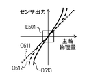
- FIG. 24A is a diagram showing an output indicating acceleration in the direction of the principal axis of the sensor in the fifth embodiment.
- FIG. 24A is a diagram showing an output indicating acceleration in the direction of the principal axis of the sensor in the fifth embodiment.
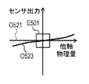
- FIG. 24B is a diagram showing an output indicating the acceleration in the direction of the other axis of the sensor according to the fifth embodiment.
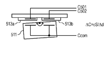
- FIG. 24C is a schematic cross-sectional view of the X detection unit of the sensor according to Embodiment 5.
- FIG. 25A is a diagram showing output characteristics indicating acceleration in the direction of the principal axis of the sensor in the fifth embodiment.
- FIG. 25B is a diagram illustrating an output characteristic indicating acceleration in the direction of the other axis of the sensor according to Embodiment 5.
- FIG. 25C is a schematic cross-sectional view of the X detection unit of the sensor according to Embodiment 5.
- FIG. 26 is a functional block diagram of the sensor in the fifth embodiment.
- FIG. 27 is a diagram illustrating the output of the X detection unit of the sensor in the fifth embodiment.
- FIG. 28A is a diagram illustrating an output obtained by correcting the output of the X detection unit by the correction circuit of the sensor of the comparative example.
- FIG. 28B is a diagram illustrating an output obtained by correcting the output of the X detection unit by the correction circuit of the sensor of the comparative example.
- FIG. 29A is a diagram illustrating an output obtained by correcting the output of the X detection unit using another correction circuit of the sensor according to the embodiment.
- FIG. 29B is a diagram showing an output obtained by correcting the output of the X detector using the correction circuit shown in FIG. 29A.
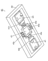
- FIG. 1 is an exploded perspective view of a sensor 701 according to the first embodiment.
- the sensor 701 in Embodiment 1 is an acceleration sensor that detects applied acceleration.
- the sensor 701 is drawn from the sensor chip 4100, an integrated circuit 4200 that performs various calculations based on the output from the sensor chip 4100, a package 4300 for arranging the sensor chip 4100 and the integrated circuit 4200, and the package 4300.
- a terminal 4400, a lead 4402 drawn from the package 4300, and a lid 4600 covering the upper surface of the package 4300 are provided.
- the integrated circuit 4200 is an application specific integrated circuit (ASIC).
- ASIC application specific integrated circuit
- the integrated circuit 4200 is electrically connected to the sensor chip 4100 through, for example, a metal wire, processes an electrical signal output from the sensor chip 4100, for example, a signal indicating acceleration, and processes the processed signal outside the package 4300. Output to.
- the lid 4600 is made of, for example, a metal material such as stainless steel, and is disposed at a position covering the opening of the package 4300. In other words, the lid 4600 is disposed at a position covering the sensor chip 4100 and the integrated circuit 4200.
- the package 4300 is made of a resin material such as a liquid crystal polymer.
- a side surface of the package 4300 facing the lead 4402 is inclined inward as the lid 4600 is closer.
- “inner side” means “the side accommodating the integrated circuit 4200 and the sensor chip 4100”. Accordingly, a large space can be formed between the lead 4402 and the package 4300, the lead 4402 can be easily bent, and the function of the lead 4402 as a spring is not hindered.
- Package 4300 accommodates sensor chip 4100 and integrated circuit 4200 inside. Terminals 4400 and leads 4402 extend from the package 4300.
- the terminal 4400 is electrically connected to a substrate outside the sensor 701.
- the lead 4402 is electrically connected to the lid 4600.
- FIG. 2 is a cross-sectional view of the sensor 701.
- the lead 4402 includes a portion 4402a and a portion 4402b connected to the portion 4402a.
- Portion 4402a extends from package 4300 and extends along the side of package 4300.
- the portion 4402a is illustrated as extending in the vertical direction, but the present invention is not limited to this. For example, it may extend along the inward inclination of the side surface of the package 4300.
- the portion 4402a is electrically connected to the ground 4404. By this.
- the potential of the lid 4600 connected to the portion 4402b can be dropped to the ground.
- the portion 4402b extends toward the inside of the package 4300 and is sandwiched between the lid 4600 and the package 4300. Thereby, the lid 4600 is electrically connected.
- the tip portion 4402b of the bent lead 4402 is pressed against the lid 4600 by the spring force of the lead 4402 itself. Accordingly, the lead 4402 can be stably electrically connected to the lid 4600.
- the portion 4402b is disposed in a recess 4300p provided on the upper edge of the package 4300.
- the depth of the recess 4300p is preferably greater than the thickness of the portion 4402b. Accordingly, a gap 4302 can be provided between the package 4300 and the lid 4600 in a state after the lid 4600 is attached. Accordingly, for example, it is possible to confirm whether the lead 4402 is in proper contact with the lid 4600 by X-ray inspection from the lateral direction, and the inspection can be simplified.
- the depth of the recess 4300p may not be larger than the thickness of the portion 4402b.
- the depth of the recess 4300p may be substantially equal to the thickness of the portion 4402b. In this case, since the upper edge of the package 4300 and the portion 4402b can be substantially matched, the package 4300 can be reduced in size.
- the tip 4402c of the portion 4402b protrudes inward from the inner wall surface 4300t along the straight line L of the package 4300. Accordingly, for example, it is possible to confirm whether the lead 4402 is properly arranged by X-ray inspection from above, and the inspection can be simplified.
- a plurality of terminals 4400 connected to the external substrate extend from the package 4300.
- FIG. 3 is an exploded perspective view of the sensor chip 4100.
- the sensor chip 4100 is a connection structure including a sensor substrate 401, a substrate 402a connected to the sensor substrate 401, and a substrate 402b connected to the sensor substrate 401.
- the substrate 402a is located above the sensor substrate 401, and the substrate 402b is located below the sensor substrate 401.
- the sensor substrate 401 is sandwiched between the substrate 402a and the substrate 402b.
- the sensor substrate 401 is formed of an SOI (Silicon On Insulator) substrate or the like.
- the substrate 402a and the substrate 402b are formed of an insulator such as glass. In other words, the substrate 402a is a glass substrate and the substrate 402b is a glass substrate.
- the sensor chip 4100 includes an X detection unit 410 that detects acceleration in the X-axis direction, a Y detection unit 420 that detects acceleration in the Y-axis direction, and a Z detection unit 430 that detects acceleration in the Z-axis direction.
- the X axis is included in the XY plane.
- the Y axis is included in the XY plane and is orthogonal to the X axis.
- the Z axis is perpendicular to the XY plane.
- the X detection unit 410 includes a rectangular frame 410a, beam portions 412a and 412b connected to the rectangular frame 410a, a movable electrode 411 supported by the beam portions 412a and 412b, and fixed electrodes 413a and 413b.
- the beam portions 412a and 412b are arranged on an axis A410 parallel to the Y axis, and are arranged on opposite sides of the movable electrode 411.
- the movable electrode 411 is connected to and supported by the rectangular frame 410a via the beam portions 412a and 412b.
- the acceleration in the X-axis direction is detected by swinging the movable electrode 411 about the axis A410.
- the axis A410 divides the upper surface of the movable electrode 411 into two parts.
- the fixed electrode 413a is opposed to one of the two parts on the upper surface of the movable electrode 411 with a gap in the Z-axis direction, and the fixed electrode 413b is spaced from the other part in the Z-axis direction. opposite. Accordingly, the acceleration in the X-axis direction can be detected based on the change in capacitance between each of the fixed electrodes 413a and 413b and the movable electrode 411.
- the Y detection unit 420 includes a rectangular frame 420a, beam portions 422a and 422b connected to the rectangular frame 420a, a movable electrode 421 supported by the beam portions 422a and 422b, and fixed electrodes 423a and 423b.
- the beam portions 422a and 422b are arranged on an axis A420 parallel to the X axis, and are arranged on opposite sides of the movable electrode 421.
- the movable electrode 421 is connected to and supported by the rectangular frame 420a via the beam portions 422a and 422b.
- the acceleration in the Y-axis direction is detected by swinging the movable electrode 421 about the axis A420.
- the axis A420 divides the upper surface of the movable electrode 421 into two parts. One of the two portions on the upper surface of the movable electrode 421 faces the fixed electrode 423a with a gap in the Z-axis direction. The other of the two parts on the upper surface of the movable electrode 421 faces the fixed electrode 423b with a gap in the Z-axis direction.
- the acceleration in the Y-axis direction can be detected based on the change in capacitance between each of the fixed electrodes 423a and 423b and the movable electrode 421.
- the Z detection unit 430 includes a rectangular frame 430a, beam units 432a, 432b, 432c, and 432d connected to the rectangular frame 430a, a movable electrode 431 supported by the beam units 432a, 432b, 432c, and 432d, and a fixed electrode 433a. 433b.
- the movable electrode 431 is connected to and supported by the rectangular frame 430a via the beam portions 432a, 432b, 432c, and 432d.
- the acceleration in the Z-axis direction is detected by translating the movable electrode 431 held by the beam units 432a, 432b, 432c, and 432d in the Z-axis direction.
- the upper surface of the movable electrode 431 faces the fixed electrode 433a with a space in the Z-axis direction
- the lower surface of the movable electrode 431 faces the fixed electrode 433b with a space in the Z-axis direction. Accordingly, the acceleration in the Z-axis direction can be detected based on the change in electrostatic capacitance between each of the fixed electrodes 433a and 433b and the movable electrode 431.
- the X detection unit 410 and the Y detection unit 420 have the same shape and are rotated by 90 ° with respect to each other.
- the Z detection unit 430 is disposed between the X detection unit 410 and the Y detection unit 420, and the X detection unit 410, the Y detection unit 420, and the Z detection unit 430 are disposed in one chip. That is, as shown in FIG. 3, the rectangular frames 410a, 420a, and 430a are arranged on a straight line in the Y-axis direction.
- a movable electrode 411 is disposed in the rectangular frame 410a, a movable electrode 421 is disposed in the rectangular frame 420a, and a movable electrode 431 is disposed in the rectangular frame 430a.
- the movable electrode 411, the movable electrode 421, and the movable electrode 431 all have a substantially rectangular shape.
- a gap having a predetermined width is provided between the movable electrode 411, the movable electrode 421, and the movable electrode 431 and the side walls of the rectangular frames 410a, 420a, and 430a.
- the shapes of the frames 410a, 420a, and 430a are not limited to a rectangular shape, and may be various shapes such as a circular shape.
- the sensor substrate 401 is bonded to the substrate 402a at the connection portion 403.
- the fixed electrodes 413a and 413b are drawn out to the upper surface of the substrate 402a using the through electrodes 414a and 414b, respectively.
- the material of the through electrodes 414a and 414b is a conductor such as silicon, tungsten, or copper, and the surrounding material that holds the through electrodes 414a and 414b is an insulator such as glass.
- the movable electrode 411 can swing freely by connecting a substantially central portion of two opposite sides of the surface of the movable electrode 411 and a side wall portion of the rectangular frame 410 a with a pair of beam portions 412 a and 412 b. Supported.
- fixed electrodes 413a and 413b are provided with an axis A410 connecting the beam portion 412a and the beam portion 412b as a boundary line.
- the fixed electrodes 413a and 413b are drawn to the upper surface of the substrate 402a using the through electrodes 414a and 414b.
- the material of the through electrodes 414a and 414b is a conductor such as silicon, tungsten, or copper, and the surrounding material that holds the through electrodes 414a and 414b is an insulator such as glass.
- the Y detection unit 420 is connected to a substantially central portion of two opposite sides of the surface of the movable electrode 421 and a side wall portion of the rectangular frame 420a by a pair of beam portions 422a and 422b.
- the movable electrode 421 is swingably supported.
- fixed electrodes 423a and 423b are provided with an axis A420 connecting the beam portion 422a and the beam portion 422b as a boundary line.
- the fixed electrodes 423a and 423b are drawn to the upper surface of the substrate 402a using the through electrodes 424a and 424b.
- the material of the through electrodes 424a and 424b is a conductor such as silicon, tungsten, and copper, and the surrounding material that holds the through electrodes 424a and 424b is an insulator such as glass.
- the Z detection unit 430 connects the four corners of the movable electrode 431 and the side wall of the rectangular frame 430a with two pairs of L-shaped beam portions 432a, 432b, 432c, and 432d, so that the movable electrode 431 is connected to the Z axis. Can move in parallel.
- the shape of the beam portions 432a, 432b, 432c, and 432d is not particularly limited, but if the shape is an L shape, the beam portions 432a, 432b, 432c, and 432d can be elongated.
- a fixed electrode 433a facing the movable electrode 431 is provided on the lower surface of the substrate 402a, and a fixed electrode 433b facing the movable electrode 431 is provided on the lower surface of the substrate 402b.
- the fixed electrode 433a is used through the through electrode 434a and drawn to the upper surface of the substrate 402a.
- the fixed electrode 433b is connected to a columnar electrode 435b separated from the movable electrode 431, and the columnar electrode 435b is connected to a through electrode 434b provided on the substrate 402a. Thereby, the fixed electrode 433b can be drawn out to the upper surface of the substrate 402a through the columnar electrode 435b and the through electrode 434b.
- the material of the through electrodes 434a and 434b is a conductor such as silicon, tungsten, or copper, and the material of the peripheral portions of the substrates 402a and 402b that hold the through electrodes 434a and 434b is an insulator such as glass.
- FIG. 4 and 5 are top perspective views of the sensor substrate 401.
- FIG. 4 some electrodes are omitted for convenience of explanation.
- each columnar electrode 435a, the columnar electrode 435b, the columnar electrode 435c, and the columnar electrode 435d are electrically insulated from each movable electrode and each beam portion, respectively.
- each columnar electrode is formed by providing a through hole in a part of the sensor substrate 401.
- the columnar electrode 435a is electrically connected to the fixed electrode 433a.
- the columnar electrode 435b is electrically connected to the fixed electrode 433b.
- the sensor substrate 401 is joined to the substrate 402a by the connecting portion 403.
- the sensor substrate 401 has a connection portion 441a and a connection portion 441b that protrude toward the substrate 402a.
- the connection portions 441a and 441b are bonded to the substrate 402a.
- Protrusions 442a and 442b are provided in the vicinity of the connecting part 441a.
- the connecting portion 441a, the convex portion 442a, and the convex portion 442b are provided at a position passing through a virtual straight line L401 parallel to the upper surface of the sensor substrate 401.
- Protrusions 442c and 442d are provided in the vicinity of the protrusions 442a and 442b. The material, structure, size, positional relationship, etc. of each convex part will be described later.
- the sensor substrate 401 has a connection portion 441d that protrudes toward the substrate 402b.
- the connection portion 441d is bonded to the substrate 402b similarly to the connection portion 441b.
- the electrode 438a is provided at a position overlapping the beam portions 432a, 432b, 432c, and 432d.
- the electrode 438a is electrically connected to the columnar electrode 435c, the columnar electrode 435d, and the through electrode 434b.
- the electrode 438b is electrically connected to the columnar electrode 435b and the through electrode 434b.
- the role of the electrode 438a will be described.
- the sensor substrate 401 can be bonded to each of the substrates 402a and 402b by anodic bonding.
- the anodic bonding is a bonding method in which the sensor substrate 401 and the substrate 402a are heated while applying a potential.
- an attractive force is generated between each movable electrode and the substrate 402a due to a potential applied to the sensor substrate 401 and the substrate 402a during anodic bonding, and each movable electrode is attached to the substrate 402a. May cause defects such as sticking.
- the potential of the electrode 438a is substantially equal to the potential of the sensor substrate 401 during anodic bonding so that each movable electrode comes into contact with the substrate 402a. This prevents the occurrence of defects such as sticking.
- the columnar electrode 435a and the columnar electrode 435b are provided at positions facing each other across the movable electrode 431.
- the columnar electrode 435c and the columnar electrode 435d are provided at positions facing each other across the movable electrode 431.
- FIG. 6 and 7 are bottom views of the sensor substrate 401.
- FIG. 6 some electrodes are omitted for convenience of explanation.
- the electrode 438c is provided around the fixed electrode 433b.
- the electrode 438c is electrically connected to the columnar electrode 435c and the columnar electrode 435d.
- the sensor substrate 401 has connection portions 441c and 441d protruding toward the substrate 402b.
- the connection portions 441c and 441d are bonded to the substrate 402b.
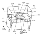
- FIG. 8A is an enlarged view of the sensor substrate 401 shown in FIG. 5, and shows an upper surface 1435a of the columnar electrode 435a.
- 8B is a cross-sectional view taken along line 8B-8B of sensor substrate 401 shown in FIG. 8A.
- the convex portion 442a, the convex portion 442b, the convex portion 442c, and the convex portion 442d are provided on the upper surface 1435a of the columnar electrode 435a, which is a part of the upper surface of the sensor substrate 401.
- the convex portion 442c and the convex portion 442d are preferably formed of the same member as the columnar electrode 435a, but may be formed of different members.
- the protrusions 442 a and 442 b are made of a metal provided on the upper surface of the oxide film 444 provided on the upper surface of the sensor substrate 401. By adjusting the thickness of the oxide film 444, the heights of the protrusions 442a and 442b can be adjusted.
- the convex portions 442a to 442d are elongated along the extending direction A402.
- the wiring 439a, the wiring 439b, the wiring 439c, and the wiring 439d electrically connect the electrodes 438c.
- the wiring 439e When viewed from above, the wiring 439e includes a linear portion 1439e extending from the end portion 439e1 to the end portion 439e2, and a linear portion 2439e extending between the end portion 439e1 and the end portion 439e2 at a right angle from substantially the middle of the linear portion 1439e. And a portion having a T shape.
- the end portion 439e1 is sandwiched between the substrate 402a and the convex portion 442a, and the end portion 439e2 is sandwiched between the substrate 402a and the convex portion 442b.
- the wiring 439e is electrically connected to each convex portion by sandwiching the wiring 439e and each convex portion between the substrate 402a and the sensor substrate 401.
- the convex portions 442c and 442d extend in the extending direction A402 parallel to the convex portions 442a and 442b, and are arranged in a direction A401 perpendicular to the extending direction A402.
- a straight line portion 1439e of the wiring 439e extends in an elongated shape in the extension cavity A402, and a straight line portion 2439e extends in a direction A401.
- the length of the convex portion 442c in the extending direction A402 is larger than the length of the convex portion 442a in the extending direction A402, and the length of the convex portion 442d in the extending direction A402 is larger than the length of the convex portion 442b in the extending direction A402.
- the width in the direction A401 of the convex part 442c and the convex part 442d is larger than the width in the direction A401 of the convex part 442a and the convex part 442b. Further, the width of the convex portion 442c in the direction A401 is substantially equal to the width of the convex portion 442d in the direction A401, and the width of the convex portion 442a in the direction A401 is substantially equal to the width of the convex portion 442b in the direction A401. In this manner, the wiring 439e and the convex portions 442a and 442b can be reliably crushed by arranging the convex portion 442c and the convex portion 442d near the stepping-down.
- the sensor chip 4100 according to Embodiment 1 includes the X detection unit 410, the Y detection unit 420, and the Z detection unit 430, but is not limited thereto.
- the sensor chip 4100 may include only the X detection unit 410 of the X detection unit 410, the Y detection unit 420, and the Z detection unit 430, or the Z detection of the X detection unit 410, the Y detection unit 420, and the Z detection unit 430. Only the part 430 may be provided.
- the sensor substrate 401 in the first embodiment includes four columnar electrodes 435a to 435d, but is not limited to this.
- the sensor substrate 401 may include only the columnar electrode 435d among the four columnar electrodes 435a to 435d.
- Z detection part 430 in Embodiment 1 is provided with fixed electrodes 433a and 433b, it is not limited to this.
- the Z detection unit 430 may include only the fixed electrode 433a among the fixed electrodes 433a and 433b.
- the movable electrode 431 is supported by the plurality of beam portions 432a to 432d, but is not limited thereto.
- the movable electrode 431 may be supported by only one beam portion.
- the movable electrode 431 also functions as a movable part and a weight part.
- the sensor 701 in the first embodiment is an acceleration sensor that detects acceleration, but is not limited thereto.
- the sensor 701 may be another sensor such as a pressure sensor that detects pressure or an angular velocity sensor that detects angular velocity.
- the senor 701 according to Embodiment 1 can be mounted on an electronic device such as a mobile phone and used for the purpose of detecting the movement of the electronic device.
- the sensor 701 can be mounted on a vehicle and used for the purpose of detecting the movement of the vehicle.
- the sensor 701 according to Embodiment 1 since the sensor 701 according to Embodiment 1 has high accuracy, it is possible to perform highly accurate electronic device motion detection or highly accurate vehicle control.
- the sensor according to the second embodiment includes a sensor chip 4100 having substrates 402a and 402b and a sensor substrate 401, similarly to the sensor 701 according to the first embodiment shown in FIGS.
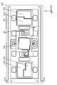
- FIG. 9 is a top view of sensor chip 4100 in the second embodiment.
- the substrate 402a is a glass substrate and transmits light. Therefore, when viewed from above, the sensor substrate 401 and electrodes such as fixed electrodes 413a and 413b provided between the sensor substrate 401 and the substrate 402a can be seen through the substrate 402a.
- the sensor substrate 401 has a connection portion 403 that is bonded to the substrate 402a.
- the connection portion 403 includes a portion 481 having a linear shape separated from the substrate 402a.
- the portion 481 of the sensor substrate 401 is not bonded to the substrate 402a.
- the sensor substrate 401 is recessed in the portion 481, the sensor substrate 401 is not in contact with the substrate 402a in the portion 481.
- Anodic bonding is a bonding method in which glass and a silicon substrate are bonded to each other by applying a voltage while heating the polishing surfaces of the glass and the silicon substrate.
- the sensor chip 4100 After heating and joining, when the temperature is returned to room temperature, the sensor chip 4100 stresses due to the difference in coefficient of linear expansion between the substrates 402a and 402b made of glass and the sensor substrate 401 formed of an SOI substrate which is a silicon substrate. Received state. At this time, the stress of the sensor chip 4100 is distributed so as to be concentrated mainly on each beam portion. This is because each beam portion is subjected to stress during anodic bonding via the connection portion 403.
- the connection portion in the sensor chip 4100 by peeling the connection portion in the sensor chip 4100 in a linear shape, the stress at the time of anodic bonding is relieved in the linearly peeled portion 481, so that the stress distribution can be changed. That is, it is possible to relax the stress received by each beam portion.
- linearly peeled portion 481 is provided along the straight lines L101 and L102.
- the linearly peeled portion 481 is provided at the connection portion 403 (distance D101 away from the inner edge of the sensor substrate 401. Thereby, the stress distribution of the sensor chip 4100 is changed over the entire surface. If the distance D101 is 50 ⁇ m or more, it is possible to maintain airtightness inside the sensor chip 4100. Preferably, the distance D101 is 100 ⁇ m or more. Is preferred.
- the linearly peeled portion 481 is at least larger than the inner edge of the sensor substrate 401 of the connection portion 403, and is provided with a length to the outer edge of the sensor substrate 401 of the connection portion 403, whereby the sensor chip 4100 is provided.
- the stress distribution can be changed over the entire surface.
- the part 481 that is peeled off in a linear shape only needs to be 1/3 or more of the entire length of the connecting portion 403, and preferably has a linear shape or a surface shape.
- connection part 403 on the long side of the sensor chip 4100 is stripped in a linear shape, but the present invention is not limited to this.
- the operation of the movable electrode 411 is unstable due to stress, only the region close to the movable electrode 411 may be peeled off.
- the operation is unstable with the movable electrode 411 and the movable electrode 421, only the region close to the movable electrode 411 and the movable electrode 421 may be peeled off.
- FIG. 10 is a top view of the sensor chip 4100P in the second embodiment.
- the sensor chip 4100P includes a sensor substrate 401P instead of the sensor substrate 401 of the sensor chip 4100 shown in FIG. 10, the same parts as those of the sensor chip 4100 shown in FIGS. 1 to 9 are denoted by the same reference numerals.
- the sensor chip 4100P shown in FIG. 10 has a groove 491 provided on the upper surface of the sensor substrate 401P.
- the connecting portion 403 is separated into a plurality of portions by the groove portion 491.
- the groove portion 491 separates the connection portion 403 into connection portions 403a and 403b.
- connection portion 403a is provided with a linearly separated portion 481, which functions as a portion for adjusting stress.
- the connection portion 403b is not provided with the linearly peeled portion 481, and is used only for connecting the sensor substrate 401P to the substrate 402a.
- connection portion 403a and the connection portion 403b are separated from each other, it is possible to avoid separation of a region other than a desired region at the time of separation. That is, even when peeling is performed, the groove portion 491 serves as a buffer, and the connection portion 403b can be prevented from being connected and the connection portion other than the desired region can be prevented from being peeled off. As a result, deterioration of the airtightness of the sensor chip 4100 can be prevented.
- the groove 491 has a depth of 1 ⁇ m or more and a width of 10 ⁇ m or more in order to prevent peeling of other than the desired connection portion.
- FIG. 11 is a top view of the sensor chip 4100Q in the second embodiment.
- the sensor chip 4100Q includes a sensor substrate 401Q instead of the sensor substrate 401P of the sensor chip 4100P shown in FIG.
- the same reference numerals are assigned to the same parts as those of the sensor chip 4100P shown in FIG.
- a groove portion 492 is provided on the upper surface of the sensor substrate 401Q. By providing the groove portion 492, the connection portion 403 is separated into more sections.
- This structure makes it possible to effectively relieve the stress received by anodic bonding for the following reasons.
- the movable electrode 411 is held by the beam portions 412a and 412b, and the movable electrode 421 is held by the beam portions 422a and 422b. That is, due to anodic bonding, the movable electrode 411 receives stress in the Y-axis direction, and the movable electrode 421 receives stress in the X-axis direction.
- the distribution of stress is effectively changed with respect to the movable electrode 411 and the movable electrode 421 by arranging the adjustment connecting portion not only on the long side but also on the short side of the sensor chip 4100. be able to.
- FIG. 12 is a top view of the sensor chip 4100R in the second embodiment.
- the sensor chip 4100R includes a sensor substrate 401R instead of the sensor substrate 401 of the sensor chip 4100 shown in FIG. 12, the same reference numerals are assigned to the same portions as those of the sensor chip 4100 shown in FIGS.
- a sensor chip 4100R shown in FIG. 12 is provided with a plurality of portions 482 each having a point shape separated from the substrate 402a on the upper surface of the sensor substrate 401R.
- the plurality of portions 482 can obtain the same effect as the portion 481 of the sensor substrate 401 shown in FIG.
- the plurality of portions 482 are provided along the straight lines L101 and L102.
- the plurality of portions 482 are provided at a distance D101 from the edge of the connection portion 403.
- the distance D101 is 50 ⁇ m or more, it is possible to maintain the airtightness inside the sensor chip 4100.
- the distance D101 is preferably 100 ⁇ m or more.
- the plurality of portions 482 illustrated in FIG. 12 have a circular shape, but are not limited to a circular shape and may have a rectangular shape.
- the plurality of portions 482 are provided in the same region as the portion 481 shown in FIG.
- the portion 481 of the sensor substrate 401 and the plurality of portions 482 of the sensor substrate 401R irradiate the connection portion 403 with a laser having a desired energy from above the sensor chip 4100R through the substrate 402a that is a glass substrate. It can be formed by peeling from the substrate 402a.
- the plurality of portions 482 are formed by irradiating the connection portion 403 with laser at predetermined intervals along the straight lines L101 and L102.
- the portion 481 of the sensor substrate 401 can be formed by irradiating a laser with a part of the spot of the irradiated laser being overlapped.
- groove portion 491 can be formed at the same time when the gap of the sensor chip 4100 is formed, thereby eliminating an additional process.
- straight line L101 and the straight line L102 do not need to pass through the exact center of the part 481 that is peeled off linearly.
- straight lines L101 and L102 can be defined as straight lines L101 and L102.
- straight lines L101 and L102 do not have to pass through the exact center of each of the plurality of portions 482 separated in a point shape.
- straight lines that pass through at least a part of each of the portions 482 that are peeled off in a dotted manner can be drawn, these can be defined as straight lines L101 and L102.
- the movable electrode 431 when an acceleration having a component in the Z-axis direction is applied from the outside, the movable electrode 431 is displaced. At this time, the distance between the movable electrode 431 and the fixed electrode 433a and the distance between the movable electrode 431 and the fixed electrode 433b change. As a result, the capacitance between the movable electrode 431 and the fixed electrode 433a and the capacitance between the movable electrode 431 and the fixed electrode 433b vary. Acceleration can be detected based on these changes in capacitance.
- the fixed electrode 433b is electrically connected to the columnar electrode 435b for the purpose of extracting the potential to the outside.
- the capacitance between the movable electrode 431 and the fixed electrode 433b includes the capacitance of the columnar electrode 435b as a parasitic capacitance.
- the capacitance between the movable electrode 431 and the fixed electrode 433a does not have the above-described structure that generates the parasitic capacitance, as a result, the capacitance between the movable electrode 431 and the fixed electrode 433a A difference occurs in the capacitance between the electrode 431 and the fixed electrode 433b. This difference in capacitance causes the characteristics such as the temperature characteristics of the sensor 701 to deteriorate.
- the sensor 701 has a structure in which parasitic capacitance is generated by electrically connecting the fixed electrode 433a and the columnar electrode 435a, and the capacitance between the movable electrode 431 and the fixed electrode 433a is the capacitance between the movable electrode 431 and the fixed electrode 433b. And substantially the same. As a result, the deterioration of the characteristics due to the difference in capacity is suppressed.
- FIG. 13 is an enlarged view of sensor 702 in the fourth embodiment having substantially the same structure as sensor 701 in the first embodiment.
- FIG. 14 is an enlarged view of the sensor 702 shown in FIG. 13 and shows a region R409.
- the sensor 702 in the fourth embodiment has basically the same structure as the sensor 701 in the first embodiment shown in FIGS.
- the fixed electrode 433a When viewed from above, the fixed electrode 433a has a side 4431a disposed outside the end of the movable electrode 431 and a side 4431b receding from the side 4431a.
- the side 4431a is positioned outside the end of the movable electrode 431 by a width W301.
- the width W301 is 5 ⁇ m.
- the side 4431b is provided at a position overlapping the end of the movable electrode 431 when viewed from above.
- the straight line L301 indicates the position of the end of the movable electrode 431.
- the movable electrode 431 and the beam portion 432b are divided with the straight line L301 as a boundary.
- the beam portion 432b undergoes deformation such as bending due to acceleration applied from the outside. Therefore, when the side 4431b is arranged closer to the beam part 432b than the straight line L301, that is, when the fixed electrode 433a extends beyond the straight line L301 and above the beam part 432b, the fixed electrode 433a is deformed by the deformation of the beam part 432b.
- the side 4431b is provided at a position overlapping the end of the movable electrode 431 when viewed from above, that is, the fixed electrode 433a extends over the line L301 and above the beam portion 432b. Therefore, such deterioration of accuracy can be suppressed.
- the electrode 438a has a side 4481a facing the side 4431a of the fixed electrode 433a and a side 4481b facing the side 4431b of the fixed electrode 433a.
- the distance D301 between the side 4431a of the fixed electrode 433a and the side 4421a of the electrode 438a is substantially equal to the distance D302 between the side 4431b of the fixed electrode 433a and the side 4481b of the electrode 438a.
- FIG. 15 is a perspective view of sensor 1000 in the fifth embodiment.
- the sensor 1000 includes a package 5300 and a lid that covers the package 5300. In FIG. 15, the lid of the package 5300 is not shown.
- the package 5300 includes a sensor chip 5100 and an integrated circuit 5200 that performs various calculations based on an output from the sensor chip 5100.
- the sensor 1000 is an acceleration sensor that detects acceleration
- the integrated circuit 5200 is an application specific integrated circuit (ASIC).
- ASIC application specific integrated circuit
- the terminal 5400 is drawn from the package 5300 and connected to an external substrate 5500.
- Sensor 1000 is a capacitance type acceleration sensor, and is manufactured by MEMS technology.
- Three weights (movable electrodes) for detecting each axis are arranged on the sensor chip 5100 in order to detect acceleration in the directions of the three axes of the X axis, the Y axis, and the Z axis perpendicular to each other.
- FIG. 16 is an exploded perspective view of the sensor chip 5100.
- the sensor chip 5100 includes a sensor unit 501, a substrate 502a bonded to the upper surface of the sensor unit 501, and a substrate 503b bonded to the lower surface of the sensor unit 501.
- the sensor unit 501 is sandwiched between the substrate 502a and the substrate 502b.
- the sensor unit 501 is formed of an SOI (Silicon on Insulator) substrate or the like, and the substrate 502a and the substrate 502b are formed of an insulator such as glass.
- the sensor unit 501 includes a frame unit 503.
- the frame unit 503 includes a rectangular frame 510a, a rectangular frame 520a, and a rectangular frame 530a arranged on a straight line.
- a movable electrode 511 is arranged inside the rectangular frame 510a, a movable electrode 521 is arranged inside the rectangular frame 520a, and a movable electrode 531 is arranged inside the rectangular frame 530a.
- the sensor unit 501 includes an X detection unit 510 that detects acceleration in the X-axis direction, a Y detection unit 520 that detects acceleration in the Y-axis direction, and a Z detection unit 530 that detects acceleration in the Z-axis direction.
- the X axis is parallel to the upper surface and the lower surface of the sensor chip 5100.
- the Y axis is parallel to the upper and lower surfaces of the sensor chip 5100 and is perpendicular to the X axis.
- the Z axis is perpendicular to the X axis and the Y axis, that is, perpendicular to the upper surface and the lower surface of the sensor chip 5100.
- the X detection unit 510 includes beam units 512a and 512b, a movable electrode 511, and fixed electrodes 513a and 513b.
- the beam portions 512a and 512b are connected to the rectangular frame 510a and support the movable electrode 511.
- the beam portions 512a and 512b are arranged along a straight line A510 parallel to the Y axis.
- the upper surface of the movable electrode 511 is divided into two parts by a straight line A511.
- the fixed electrode 513a is opposed to one of the two portions on the upper surface of the movable electrode 511 divided by the straight line A510 with a space in the Z-axis direction, and the fixed electrode 513b is divided by the straight line A510.
- the other of the two parts on the upper surface of the movable electrode 511 is opposed to the other in a Z-axis direction.
- the X detection unit 510 performs acceleration in the X-axis direction based on a change in capacitance between the movable electrode 511 and the fixed electrode 513a and a change in capacitance between the movable electrode 511 and the fixed electrode 513b. Is detected.
- the Y detection unit 520 includes beam units 522a and 522b, a movable electrode 521, and fixed electrodes 523a and 523b.
- the Y detection unit 520 has the same structure as the X detection unit 510 and coincides with the X detection unit 510 rotated by 90 °.
- the shape of each component of the Y detector 520 is the same as that of the X detector 510.
- the Y detection unit 520 includes beam units 522a and 522b, a movable electrode 521, and fixed electrodes 523a and 523b.
- the beam portions 522a and 522b are connected to the rectangular frame 520a and support the movable electrode 521.
- the beam portions 522a and 522b are arranged along a straight line A520 parallel to the X axis.
- the upper surface of the movable electrode 521 is divided into two parts by a straight line A520.
- One of the two parts of the upper surface of the movable electrode 521 divided by the fixed electrode 523a straight line A520 is opposed to the upper part of the movable electrode 521 divided by the fixed electrode 523b straight line A520, and is opposed to one of the two parts on the upper surface of the movable electrode 521.
- the Y detector 520 accelerates in the Y-axis direction based on the change in capacitance between the movable electrode 521 and the fixed electrode 523a and the change in capacitance between the movable electrode 521 and the fixed electrode 523b. Is detected.
- the beam units 532a, 532b, 532c, and 532d are connected to the rectangular frame 530a and support the movable electrode 531.
- the fixed electrode 533a is opposed to the upper surface of the movable electrode 531 in the Z-axis direction
- the fixed electrode 533b is opposed to the lower surface of the movable electrode 531 in the Z-axis direction.
- the Z detection unit 530 accelerates in the Z-axis direction based on a change in capacitance between the movable electrode 531 and the fixed electrode 533a and a change in capacitance between the movable electrode 531 and the fixed electrode 533b. Is detected.
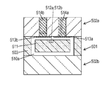
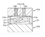
- FIG. 17A is a cross-sectional view of the X detection unit 510
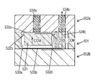
- FIG. 17B is a cross-sectional view of the Z detection unit 530.
- the cross section of the Y detector 520 is the same as that of the X detector 510.
- the fixed electrode 513a and the fixed electrode 513b are drawn to the upper surface of the substrate 502a using the through electrode 514a and the through electrode 514b.
- a fixed electrode 533a is provided in a portion of the substrate 502a facing the movable electrode 531 and a fixed electrode 533b is provided in a portion of the substrate 502b facing the movable electrode 531. Thereby, in the fixed electrode 533a, the electric signal from the through electrode 534a is drawn to the upper surface of the substrate 502a.
- the fixed electrode 533b includes a protruding region 533b2 protruding from the rectangular region 533b1 (see FIG. 16).
- the protruding region 533b2 is connected to a columnar fixed electrode 534c separated from the movable electrode 531, and the columnar fixed electrode 534c is connected to a through electrode 534b provided on the substrate 502a.
- the electric signal from the fixed electrode 533b is drawn out to the upper surface of the substrate 502a using the columnar fixed electrode 534c and the through electrode 534b.
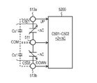
- FIGS. 18 and 19 are a cross-sectional view and a circuit diagram of the X detection unit 510 in a state where no acceleration in the X-axis direction is applied, respectively.
- the electrostatic capacitance C501 between the movable electrode 511 and the fixed electrode 513a is the electrostatic capacitance between the movable electrode 511 and the fixed electrode 513b, as shown in FIG.
- a parasitic capacitance Cs1 between the fixed electrodes 513a and 513b and the movable electrode 511 is equal to the capacitance C502.
- the capacitance C501 between the movable electrode 511 and the fixed electrode 513a is the sum (Cs1 + ⁇ C) of the parasitic capacitance Cs1 and the change ⁇ C, and the capacitance between the movable electrode 511 and the fixed electrode 513b.
- the capacitance C502 between them is a difference (Cs1 ⁇ C) obtained by subtracting the change ⁇ C from the parasitic capacitance Cs1.
- the X detection unit 510 detects the acceleration in the X direction based on the change in capacitance. Similar to the X detection unit 510, the Y detection unit 520 detects acceleration in the Y-axis direction.
- the capacitance C505 between the movable electrode 531 and the fixed electrode 533a is the sum (Cs2 + ⁇ C) of the parasitic capacitance Cs2 and the change ⁇ C, and the capacitance between the movable electrode 531 and the fixed electrode 533b.
- the capacitance C506 in the meantime is a difference (Cs2 ⁇ C) obtained by subtracting the change ⁇ C from the parasitic capacitance Cs2.
- the Z detection unit 530 detects the acceleration in the Z direction based on the change in the capacitance.
- the axis that detects the acceleration among the three axes is defined as the main axis, and the other axis of the main axis is defined as the other axis.
- the acceleration sensor if acceleration in the direction of the other axis is applied while acceleration in the direction of the main axis is applied, the output in the direction of the main axis may be different from the acceleration in the direction of the actual main axis.
- the integrated circuit 5200 includes a correction circuit. As a result, the influence of the acceleration in the direction of the other axis on the output indicating the acceleration in the direction of the main axis is mitigated.
- the reference state is a state where no acceleration in the direction of the other axis is applied.
- the correction state acceleration in the direction of the other axis is applied, and correction is necessary.
- the operation of the sensor 1000 when the main axis is the X axis and the other axis is the Z axis will be described.
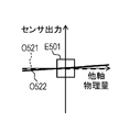
- FIG. 24A shows the output of the X detector 510 showing the acceleration in the direction of the X axis that is the main axis of the sensor 1000 in the reference state
- FIG. 24B shows the acceleration in the direction of the Z axis that is the other axis.
- the output of the Z detection part 530 shown is shown.
- FIG. 24C is a cross-sectional view of the X detection unit 510 that detects acceleration in the direction of the X axis, which is the main axis.
- the straight lines O511 and O521 shown in the figure indicate ideal outputs, and the curves O512 and O522 indicate actual outputs. That is, in an ideal sensor, the output is proportional to the applied acceleration, but the actual output includes an error. Therefore, only the output in the linear region E501 whose output is proportional to the applied acceleration may be used, and the output outside the linear region E501 may be corrected by the integrated circuit 5200.
- FIG. 25A shows the output of the X detection unit 510 indicating the acceleration of the X axis that is the main axis in the correction state
- FIG. 25B shows the Z detection unit indicating the acceleration of the Z axis that is the other axis in the correction state.
- 530 output is shown.
- FIG. 25C is a cross-sectional view of the X detection unit 510 in a corrected state. In the corrected state, as shown in FIG. 25B, the influence from the other axis is relatively large. Therefore, as shown in FIG. 25A, the difference between the curve O513 indicating the output of the spindle and the straight line O511 indicating the ideal output is larger than that in the reference state.
- the inclination of the movable electrode 511 increases and the gap d decreases.
- the capacitance change ⁇ C is increased, and the sensitivity is increased.
- FIG. 26 is a functional block diagram of the sensor 1000 according to the fifth embodiment.
- the integrated circuit 5200 includes a correction circuit 5210 that corrects the sensitivity of each axis due to the change in the gap d. The operation of the correction circuit 5210 will be described.
- the correction circuit of the comparative example corrects the output Xout1 from the X detection unit 510 generated by the acceleration in the direction of the X axis, which is the main axis, to obtain the output Xout2.
- the output Xout2 is a signal obtained by removing the other axis sensitivity that is an offset included in Xout1 due to the acceleration in the direction of the Z axis, which is the other axis, from the output Xout1.
- the correction circuit of the comparative example uses the correction coefficient AGCcode and the output Zout output from the Z detection unit 530 for the acceleration in the direction of the Z axis, which is the other axis, to obtain the output Xout2 by Expression 1.
- Xout2 Xout1 / (1-AGCcode ⁇ Zout) (Formula 1)
- the correction circuit of the comparative example corrects the output Xout1 by changing the correction coefficient (1 / (1-AGCcode ⁇ Zout)). Specifically, the output Xout1 is linearly corrected so that the output Xout1 is amplified when the output Zout is positive and the output Xout1 is attenuated when the output Zout is negative.
- FIG. 27 shows the sensitivity of the X detector 510 with respect to the acceleration in the X-axis direction, which is the main axis, with respect to the acceleration in the Z-axis direction, which is the other axis.
- the sensitivity change of the X detection unit 510 differs depending on whether the acceleration applied in parallel to the Z axis is positive or negative.
- the gap d becomes small, and the change in sensitivity with respect to the acceleration in the X axis direction increases.
- positive acceleration is applied to the Z-axis, that is, acceleration in the positive direction opposite to the negative direction of the Z-axis
- the gap d increases, so that the change in sensitivity to the acceleration in the X-axis direction decreases.
- the change in sensitivity of the X detector 510 differs in the direction of acceleration parallel to the Z axis.
- Equation 1 used in the correction circuit of the sensor of the comparative example, when the correction coefficient AGCcode is calculated so that the change in sensitivity with respect to the acceleration in the X-axis direction is zero according to the positive acceleration in the Z-axis, FIG. As shown, the sensitivity to the acceleration in the X-axis direction changes with respect to the negative acceleration in the Z-axis, and the output Xout1 cannot be corrected correctly.
- the correction circuit 5210 of the sensor 1000 is configured to change the expression used for correction according to the direction of acceleration parallel to the Z axis. Specifically, when the direction of acceleration parallel to the Z axis is the positive direction of the Z axis (Zout> 0), the correction circuit 5210 uses the weighting variable W501 to calculate the X detection unit 510 using the following equation (2). The output Xout1 is corrected to obtain the output Xout2, and when the acceleration direction is not the positive direction of the Z axis, that is, the negative direction (Zout ⁇ 0), using the weighting variable W502, The output Xout1 of the X detector 510 is corrected to obtain an output Xout2.
- W501 and W502 for weighting are variables for weighting the correction coefficient, and are determined as follows.
- the positive sensitivity Sp which is the sensitivity to the acceleration in the X-axis direction of the X detection unit 510 when a certain amount of acceleration in the positive direction of the Z-axis is applied.
- the negative sensitivity Sn which is the sensitivity to the acceleration in the X-axis direction of the X detection unit 510 when the acceleration in the negative direction of the Z-axis is applied, is obtained.
- either one of the output Xout2 in which the Z-axis acceleration is in the positive direction or the negative direction is made to correspond to the acceleration correctly may be selected.
- the influence of the other axis can be accurately suppressed regardless of whether the sign (direction) of the acceleration of the Z axis, that is, the other axis is positive or negative.
- the influence of the acceleration in the direction of the other axis on the output indicating the acceleration in the direction of the main axis can be mitigated, and the output characteristics of the detection unit that detects the acceleration of the main axis can be improved.
- the correction circuit 5210 may correct the output Xout1 by the following method using another equation.
- FIG. 29A shows the output characteristic of the X detection unit 510 obtained by Expression 4.
- FIG. 29B shows the output characteristics of the output Xout22 corrected using Equation 5.
- the sensitivity of the Y detector 520 can be corrected using the same method as the method of correcting the sensitivity of the X detector 510.
- the X axis (Y axis) is the main axis and the Z axis is the other axis, but the main axis and the other axis can be changed as appropriate.
- three MEMS structures (X detection unit 510, Y detection unit 520, and Z detection unit 530) that detect accelerations in the directions of the three axes of the X axis, the Y axis, and the Z axis, respectively.
- the output indicating the acceleration in the X-axis direction, the output indicating the acceleration in the Y-axis direction, and the output indicating the acceleration in the Z-axis direction are output from one MEMS structure.
- the output of the main axis can be corrected by the output of the other axis.
- the shape, size, layout, and the like of the sensor chip 5100 can be changed as appropriate.
- each through electrode is a conductor such as silicon, tungsten, or copper, and the surrounding material that holds each through electrode is an insulator such as glass.
- the shape of the beam portions 532a, 532b, 532c, and 532d is not limited to the L shape, but an L shape is preferable because the beam portions 532a, 532b, 532c, and 532d can be elongated. .
- arithmetic correction by a digital circuit for the correction circuit 5210.
- various corrections such as sensitivity adjustment and offset adjustment can be performed.
- terms indicating directions such as “upper surface”, “lower surface”, “upper”, and “lower” indicate relative directions determined only by the relative positional relationship of sensor components such as the sensor substrate. It does not indicate an absolute direction such as a vertical direction.
Landscapes
- Physics & Mathematics (AREA)
- General Physics & Mathematics (AREA)
- Pressure Sensors (AREA)
Abstract
Priority Applications (2)
| Application Number | Priority Date | Filing Date | Title |
|---|---|---|---|
| JP2017556317A JP6704126B2 (ja) | 2015-12-17 | 2016-11-02 | 接続構造体 |
| US15/760,615 US10649000B2 (en) | 2015-12-17 | 2016-11-02 | Connection assembly |
Applications Claiming Priority (10)
| Application Number | Priority Date | Filing Date | Title |
|---|---|---|---|
| JP2015-245850 | 2015-12-17 | ||
| JP2015245850 | 2015-12-17 | ||
| JP2015-248158 | 2015-12-21 | ||
| JP2015-248157 | 2015-12-21 | ||
| JP2015248158 | 2015-12-21 | ||
| JP2015248157 | 2015-12-21 | ||
| JP2015250136 | 2015-12-22 | ||
| JP2015-250136 | 2015-12-22 | ||
| JP2016-057958 | 2016-03-23 | ||
| JP2016057958 | 2016-03-23 |
Publications (1)
| Publication Number | Publication Date |
|---|---|
| WO2017104103A1 true WO2017104103A1 (fr) | 2017-06-22 |
Family
ID=59056181
Family Applications (1)
| Application Number | Title | Priority Date | Filing Date |
|---|---|---|---|
| PCT/JP2016/004792 Ceased WO2017104103A1 (fr) | 2015-12-17 | 2016-11-02 | Structure de connexion |
Country Status (3)
| Country | Link |
|---|---|
| US (1) | US10649000B2 (fr) |
| JP (1) | JP6704126B2 (fr) |
| WO (1) | WO2017104103A1 (fr) |
Cited By (1)
| Publication number | Priority date | Publication date | Assignee | Title |
|---|---|---|---|---|
| US11231438B2 (en) | 2018-12-25 | 2022-01-25 | Seiko Epson Corporation | Inertial sensor, electronic device, and vehicle |
Families Citing this family (1)
| Publication number | Priority date | Publication date | Assignee | Title |
|---|---|---|---|---|
| JP7394352B2 (ja) * | 2019-03-26 | 2023-12-08 | パナソニックIpマネジメント株式会社 | 信号処理装置、慣性力センサ、信号処理方法、及びプログラム |
Citations (4)
| Publication number | Priority date | Publication date | Assignee | Title |
|---|---|---|---|---|
| US5006920A (en) * | 1987-03-18 | 1991-04-09 | Telenorma Telefonbau Und Normalzeit Gmbh | Electrical components |
| US6566149B1 (en) * | 1998-09-16 | 2003-05-20 | Hitachi, Ltd. | Method for manufacturing substrate for inspecting semiconductor device |
| JP2011114054A (ja) * | 2009-11-25 | 2011-06-09 | Dainippon Printing Co Ltd | センサーユニットおよびその製造方法 |
| WO2015155983A1 (fr) * | 2014-04-08 | 2015-10-15 | パナソニックIpマネジメント株式会社 | Capteur |
Family Cites Families (47)
| Publication number | Priority date | Publication date | Assignee | Title |
|---|---|---|---|---|
| US3737729A (en) * | 1971-06-14 | 1973-06-05 | Zeltex Inc | Electronic package and method of construction |
| JPS5481073A (en) | 1977-12-12 | 1979-06-28 | Seiko Instr & Electronics Ltd | Sealing method for semiconductor element |
| US4879589A (en) * | 1988-01-25 | 1989-11-07 | Semetex Corporation | Hermetic leadless semiconductor device package |
| US5691885A (en) * | 1992-03-17 | 1997-11-25 | Massachusetts Institute Of Technology | Three-dimensional interconnect having modules with vertical top and bottom connectors |
| WO1993019432A1 (fr) * | 1992-03-17 | 1993-09-30 | Massachusetts Institute Of Technology | Systeme d'interconnexion tridimensionnelle presentant une configuration de proximite etroite |
| US5854534A (en) * | 1992-08-05 | 1998-12-29 | Fujitsu Limited | Controlled impedence interposer substrate |
| EP0586888B1 (fr) * | 1992-08-05 | 2001-07-18 | Fujitsu Limited | Module multi-chips à trois dimensions |
| JPH07113708A (ja) | 1993-10-20 | 1995-05-02 | Hitachi Ltd | 半導体絶対圧力センサの製造方法 |
| US5969259A (en) * | 1995-04-07 | 1999-10-19 | Sensym, Inc. | Side port package for micromachined fluid sensor |
| JP3278363B2 (ja) * | 1996-11-18 | 2002-04-30 | 三菱電機株式会社 | 半導体加速度センサ |
| JPH1123610A (ja) | 1997-07-08 | 1999-01-29 | Omron Corp | 静電容量型多軸加速度検出装置 |
| US6040625A (en) * | 1997-09-25 | 2000-03-21 | I/O Sensors, Inc. | Sensor package arrangement |
| JP2000164741A (ja) | 1998-11-26 | 2000-06-16 | Toyota Motor Corp | 半導体装置 |
| US6404046B1 (en) * | 2000-02-03 | 2002-06-11 | Amkor Technology, Inc. | Module of stacked integrated circuit packages including an interposer |
| US6518659B1 (en) * | 2000-05-08 | 2003-02-11 | Amkor Technology, Inc. | Stackable package having a cavity and a lid for an electronic device |
| US6492699B1 (en) * | 2000-05-22 | 2002-12-10 | Amkor Technology, Inc. | Image sensor package having sealed cavity over active area |
| US6343940B1 (en) * | 2000-06-19 | 2002-02-05 | Advantest Corp | Contact structure and assembly mechanism thereof |
| TW492114B (en) * | 2000-06-19 | 2002-06-21 | Advantest Corp | Method and apparatus for edge connection between elements of an integrated circuit |
| US6701786B2 (en) * | 2002-04-29 | 2004-03-09 | L-3 Communications Corporation | Closed loop analog gyro rate sensor |
| JP5192232B2 (ja) * | 2004-06-21 | 2013-05-08 | カプレス・アクティーゼルスカブ | プローブの位置合せを行なう方法 |
| US7238999B2 (en) * | 2005-01-21 | 2007-07-03 | Honeywell International Inc. | High performance MEMS packaging architecture |
| WO2006126441A1 (fr) * | 2005-05-26 | 2006-11-30 | Murata Manufacturing Co., Ltd. | Boitier de composant electronique et son procede de production et composant electronique utilisant ce boitier |
| US7481113B2 (en) * | 2005-07-27 | 2009-01-27 | Ricoh Company, Ltd. | Semiconductor sensor with projection for preventing proof mass from sticking to cover plate |
| JP5105736B2 (ja) * | 2005-10-31 | 2012-12-26 | 株式会社東芝 | プリント回路板、電子機器、およびプリント回路板の製造方法 |
| FI119729B (fi) * | 2005-11-23 | 2009-02-27 | Vti Technologies Oy | Menetelmä mikroelektromekaanisen komponentin valmistamiseksi ja mikroelektromekaaninen komponentti |
| JP4692373B2 (ja) | 2006-04-28 | 2011-06-01 | パナソニック電工株式会社 | 静電容量式センサ |
| JP4403424B2 (ja) * | 2006-11-30 | 2010-01-27 | ソニー株式会社 | 固体撮像装置 |
| WO2009120900A2 (fr) * | 2008-03-26 | 2009-10-01 | Endevco Corporation | Système d’interconnexion sur un plan adjacent à une structure de dispositif à semiconducteur |
| US8080925B2 (en) * | 2008-09-23 | 2011-12-20 | Custom Sensors & Technologies, Inc. | Inertial sensor with dual cavity package and method of fabrication |
| US8193555B2 (en) * | 2009-02-11 | 2012-06-05 | Megica Corporation | Image and light sensor chip packages |
| US20120037211A1 (en) * | 2009-04-15 | 2012-02-16 | Sunovel (Shzhou) Technologies Limited | Thin Film of Solar Battery Structure, Thin Film of Solar Array and Manufacturing Method Thereof |
| US8584522B2 (en) * | 2010-04-30 | 2013-11-19 | Qualcomm Mems Technologies, Inc. | Micromachined piezoelectric x-axis gyroscope |
| US8618620B2 (en) * | 2010-07-13 | 2013-12-31 | Infineon Technologies Ag | Pressure sensor package systems and methods |
| JP5791294B2 (ja) * | 2011-02-11 | 2015-10-07 | キヤノン株式会社 | 静電容量型電気機械変換装置 |
| JPWO2012124282A1 (ja) * | 2011-03-11 | 2014-07-17 | パナソニック株式会社 | センサ |
| WO2012144048A1 (fr) * | 2011-04-21 | 2012-10-26 | 株式会社日立製作所 | Appareil de mesure de grandeurs dynamiques |
| JP2013079895A (ja) | 2011-10-05 | 2013-05-02 | Panasonic Corp | 半導体物理量センサ |
| JP2013156066A (ja) * | 2012-01-27 | 2013-08-15 | Wacom Co Ltd | 静電容量方式圧力センシング半導体デバイス |
| US8810023B2 (en) * | 2012-07-06 | 2014-08-19 | Texas Instruments Incorporated | Cantilever packages for sensor MEMS (micro-electro-mechanical system) |
| JP6074854B2 (ja) | 2013-06-06 | 2017-02-08 | パナソニックIpマネジメント株式会社 | 加速度センサ |
| WO2014057623A1 (fr) | 2012-10-12 | 2014-04-17 | パナソニック株式会社 | Capteur d'accélération |
| DE102013101732A1 (de) * | 2013-02-21 | 2014-08-21 | Epcos Ag | Sensorsystem |
| JP2015010856A (ja) | 2013-06-27 | 2015-01-19 | パナソニック株式会社 | 加速度センサ |
| DE102014202821B4 (de) * | 2014-02-17 | 2023-03-30 | Robert Bosch Gmbh | Gehäuse für ein mikromechanisches Sensorelement |
| CN107110726A (zh) * | 2014-12-24 | 2017-08-29 | 株式会社藤仓 | 压力传感器以及压力传感器模块 |
| US10015882B1 (en) * | 2015-01-05 | 2018-07-03 | Qorvo Us, Inc. | Modular semiconductor package |
| WO2016114114A1 (fr) * | 2015-01-15 | 2016-07-21 | パナソニックIpマネジメント株式会社 | Capteur |
-
2016
- 2016-11-02 JP JP2017556317A patent/JP6704126B2/ja not_active Expired - Fee Related
- 2016-11-02 WO PCT/JP2016/004792 patent/WO2017104103A1/fr not_active Ceased
- 2016-11-02 US US15/760,615 patent/US10649000B2/en active Active
Patent Citations (4)
| Publication number | Priority date | Publication date | Assignee | Title |
|---|---|---|---|---|
| US5006920A (en) * | 1987-03-18 | 1991-04-09 | Telenorma Telefonbau Und Normalzeit Gmbh | Electrical components |
| US6566149B1 (en) * | 1998-09-16 | 2003-05-20 | Hitachi, Ltd. | Method for manufacturing substrate for inspecting semiconductor device |
| JP2011114054A (ja) * | 2009-11-25 | 2011-06-09 | Dainippon Printing Co Ltd | センサーユニットおよびその製造方法 |
| WO2015155983A1 (fr) * | 2014-04-08 | 2015-10-15 | パナソニックIpマネジメント株式会社 | Capteur |
Cited By (1)
| Publication number | Priority date | Publication date | Assignee | Title |
|---|---|---|---|---|
| US11231438B2 (en) | 2018-12-25 | 2022-01-25 | Seiko Epson Corporation | Inertial sensor, electronic device, and vehicle |
Also Published As
| Publication number | Publication date |
|---|---|
| US20180267079A1 (en) | 2018-09-20 |
| JPWO2017104103A1 (ja) | 2018-10-04 |
| JP6704126B2 (ja) | 2020-06-03 |
| US10649000B2 (en) | 2020-05-12 |
Similar Documents
| Publication | Publication Date | Title |
|---|---|---|
| JP4931713B2 (ja) | 力学量センサ | |
| US10534013B2 (en) | Sensor | |
| CN102313821A (zh) | 物理量传感器以及电子设备 | |
| US7290449B2 (en) | Physical quantity sensor having angular speed sensor and acceleration sensor | |
| JP6704126B2 (ja) | 接続構造体 | |
| KR20170015105A (ko) | 전기적 보상을 하는 마이크로 전기 기계 시스템 디바이스 및 그 판독출력 회로 | |
| WO2016075761A1 (fr) | Capteur d'accélération | |
| US8026594B2 (en) | Sensor device and production method therefor | |
| CN110114650B (zh) | 压力传感器元件和具备该压力传感器元件的压力传感器模块 | |
| US20160061857A1 (en) | Resonant sensor | |
| JP2016070670A (ja) | センサ装置 | |
| US10072930B2 (en) | Angular velocity sensor | |
| JP2018115891A (ja) | 加速度センサ | |
| JP5631529B2 (ja) | 加速度センサ | |
| US20210063155A1 (en) | Vibrator device | |
| US20160091526A1 (en) | Sensor | |
| JP2015017819A (ja) | 加速度センサ | |
| WO2014057623A1 (fr) | Capteur d'accélération | |
| JP6354603B2 (ja) | 加速度センサおよび加速度センサの実装構造 | |
| JP5606696B2 (ja) | 力学量センサおよびその製造方法 | |
| JP4525452B2 (ja) | 多軸加速度センサ | |
| JPH11337342A (ja) | 半導体角速度センサおよびその製造方法 | |
| JP3178143B2 (ja) | 静電容量式加速度センサ | |
| JP2005257504A (ja) | 物理量センサ装置 | |
| JP6032407B2 (ja) | 加速度センサ |
Legal Events
| Date | Code | Title | Description |
|---|---|---|---|
| 121 | Ep: the epo has been informed by wipo that ep was designated in this application |
Ref document number: 16875093 Country of ref document: EP Kind code of ref document: A1 |
|
| ENP | Entry into the national phase |
Ref document number: 2017556317 Country of ref document: JP Kind code of ref document: A |
|
| WWE | Wipo information: entry into national phase |
Ref document number: 15760615 Country of ref document: US |
|
| NENP | Non-entry into the national phase |
Ref country code: DE |
|
| 122 | Ep: pct application non-entry in european phase |
Ref document number: 16875093 Country of ref document: EP Kind code of ref document: A1 |