WO2017163390A1 - Carte de circuit imprimé et procédé de fabrication de carte de circuit imprimé - Google Patents
Carte de circuit imprimé et procédé de fabrication de carte de circuit imprimé Download PDFInfo
- Publication number
- WO2017163390A1 WO2017163390A1 PCT/JP2016/059536 JP2016059536W WO2017163390A1 WO 2017163390 A1 WO2017163390 A1 WO 2017163390A1 JP 2016059536 W JP2016059536 W JP 2016059536W WO 2017163390 A1 WO2017163390 A1 WO 2017163390A1
- Authority
- WO
- WIPO (PCT)
- Prior art keywords
- component
- circuit board
- printed circuit
- coating material
- printed
- Prior art date
- Legal status (The legal status is an assumption and is not a legal conclusion. Google has not performed a legal analysis and makes no representation as to the accuracy of the status listed.)
- Ceased
Links
Images



Classifications
-
- H—ELECTRICITY
- H05—ELECTRIC TECHNIQUES NOT OTHERWISE PROVIDED FOR
- H05K—PRINTED CIRCUITS; CASINGS OR CONSTRUCTIONAL DETAILS OF ELECTRIC APPARATUS; MANUFACTURE OF ASSEMBLAGES OF ELECTRICAL COMPONENTS
- H05K3/00—Apparatus or processes for manufacturing printed circuits
-
- H—ELECTRICITY
- H05—ELECTRIC TECHNIQUES NOT OTHERWISE PROVIDED FOR
- H05K—PRINTED CIRCUITS; CASINGS OR CONSTRUCTIONAL DETAILS OF ELECTRIC APPARATUS; MANUFACTURE OF ASSEMBLAGES OF ELECTRICAL COMPONENTS
- H05K3/00—Apparatus or processes for manufacturing printed circuits
- H05K3/22—Secondary treatment of printed circuits
- H05K3/28—Applying non-metallic protective coatings
Definitions
- the present invention relates to a printed circuit board on which connector parts and the like are mounted.
- Patent Document 1 JP 2010-10498 A (Patent Document 1).
- This publication states that “a component with a slag part is soldered by solder printing and reflowing the slag part, and a footprint 13 for mounting the slag part and a through via provided in the footprint 13 for mounting the slag part.
- 11 is a component mounting method for mounting on a printed board having an information printing ink or component fixing adhesive 14 or a component mounting step in the step of mounting the slag-attached component on the printed board 10. It is described that the component 14 that closes the hole is subjected to a step of closing the hole of the through via 11 before mounting the component, and then component mounting, solder printing, and reflow are performed ”(see summary).
- a coating material such as varnish
- the coating material prevents moisture absorption and dust from adhering to the surface of the printed circuit board and the mounted components, and at the same time has an effect of blocking electrical conduction.
- the coating material is a low-viscosity liquid to ensure a uniform coating finish.
- an application device is used in consideration of work efficiency, and it is applied automatically and manually by spraying and moving the coating material over a wide range from the device nozzle for spraying the coating material. In this operation, it is difficult to control the delicate application of the coating material having low viscosity and high permeability.
- the coating material is applied by a coating apparatus while avoiding these components and the component peripheral area of the mounting surface.
- coating materials are not normally prohibited on the opposite side of component mounting.
- the coating material may adhere to the component terminals through the through vias provided for connecting the wiring (copper foil pattern) between the substrate layers, and there is a possibility that an electrical connection failure may occur.
- the coating application cost becomes high.
- the amount of coating is adjusted while considering penetration into the parts where coating material adhesion is to be prevented.
- manual repair using a brush or the like is required.
- Patent Document 1 in a line (process) for mounting components on a printed board, a through via is blocked to prevent the solder from protruding to the back surface of the printed board in a simple process. (See paragraph 0013), and Patent Document 1 has a different purpose from the present invention that avoids connection failure due to coating material application after component mounting. Further, “the hole of the through via 11 is formed by the information printing ink or the component fixing adhesive 14 in the step of mounting the component with the slag portion on the printed board 10 or the component 14 which closes the hole in the component mounting step. Through the plugging process before mounting the components, component mounting, solder printing, and reflow are performed (see summary). Is to block.
- the coating material adheres to the component terminal via the through via without requiring an additional step to the printed circuit board between the printed circuit board production process and the component mounting process to the printed circuit board. It is an object of the present invention to provide a printed circuit board and a method for manufacturing the same that can prevent the above-described problem and reduce the cost of applying a corrosion-preventing coating material.
- the first surface on which the component is arranged and the second surface opposite to the first surface are coated with a coating material, and penetrate the first surface and the second surface.
- an additional process to the printed circuit board is not required between the printed circuit board production process and the component mounting process to the printed circuit board, and the coating material is prevented from adhering to the component terminals through the through vias and corroded. It is possible to provide a printed circuit board capable of reducing the cost of applying the prevention coating material and a method for manufacturing the same.
- FIG. 4 is a flowchart showing the flow of the production process of the printed circuit board (bare board) and the component mounting process on the printed circuit board. 1, 5, and 6 shown in the flow are described with a two-layer double-sided substrate, the same description can be applied to a multilayer substrate.
- the production process of a printed circuit board (bare board) having a circuit pattern will be described with reference to FIGS.
- the printed circuit board 1 is initially in a state of a copper clad plate in which copper foil is stretched over the entire front and back surfaces.
- a double-sided two-layer substrate it is also called a base material.
- an inner layer having a wiring pattern formed inside the printed board 1 is combined.
- a through-hole 11 for making interlayer connection to the printed circuit board 1 and an insertion-type component described in the third embodiment a through-hole for mounting the component is formed as shown in FIG. Drill holes in the same way.
- the inner wall of the hole is subjected to conduction plating as shown in FIG.
- the circuit pattern on the surface of the printed circuit board, and the component pad 12 for soldering the component terminal and the circuit pattern remove the unnecessary copper foil by etching the copper foil stretched on the front and back of the printed circuit board 1. By doing so, it is formed as shown in FIG.
- the solder that joins the component pad 12 and the component terminal in soldering flow, reflow, and manual soldering) in component mounting is supplied to and held accurately on the component pad 12, and other circuit patterns are provided.
- a resist 13 is applied to a circuit pattern other than the component pads 12 as shown in FIG.
- the silk printing process in order to be able to confirm the component mounting position at the time of component mounting, inspection after component mounting, debugging, maintenance, etc., information related to components such as component outline and component symbols on the front or back side of the printed circuit board, It is printed on the surface of the printed board as shown by silk 15 in FIG.
- the silk 14a is provided immediately below the component prohibited from adhering to the coating material, around the component, and on the rear surface of the component mounting portion, thereby closing the through-via hole.
- a component (connector) 2 is mounted using this printed circuit board 1 and soldered with solder 3 to form a component mounting substrate shown in FIG.
- 22 is a component terminal connected to a connector (not shown), and 21 is a connection terminal connected to the component pad 12. Furthermore, the state which apply
- FIG. 7 shows a printed circuit board produced without applying the present invention. It differs from FIG. 5 (f) described above in that there is no silk 14a.
- a component mounting board shown in FIG. 8 is configured by mounting the component (connector) 2 using the printed board 1 and soldering with the solder 3. Furthermore, the state which apply
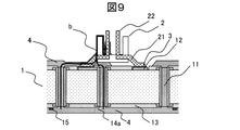
- the coating material 4 may be applied in consideration of the component mounting state of the solder surface, and coating of the coating material on the back surface (solder surface) of the component (connector) 2 is prohibited. do not do. Therefore, the coating material 4 cannot be prevented from penetrating from the through via 11 of the printed circuit board 1 into the component terminal 22 via the substrate surface and further through the external surface of the component 2 as shown in the coating material penetration route b of FIG. . Further, as a method for preventing the coating material penetration route b from being formed, it is only necessary to avoid the application of the coating material to the through via 11 on the back surface (solder surface) of the component (connector) 2. A circuit pattern exists.
- the coating material penetration is performed by printing the silk (coating material penetration preventing member) 14a on the through via 11 around the part to be prevented from penetrating the coating material in advance. Perform route disconnection.
- the range of the silk (coating material penetration preventing member) 14a to be printed is determined in the board design, and no difference occurs in the bare board production process.
- FIG. 1 is an explanatory view showing a first embodiment of a component-mounting printed board to which the present invention is applied.
- the component mounting printed circuit board is composed of a combination of a printed circuit board (bare board) 1, a component 2, solder 3, and a coating material 4.
- the printed board 1 has a copper foil, a through via 11 made of copper plating, a component pad 12 formed by etching the copper foil, and a circuit pattern (not shown).
- the through via 11 is provided for the purpose of electrically connecting the component pads 12 and circuit patterns formed on the front and back of the printed board 1 and the circuit pattern of the inner layer.
- a resist 13 is applied to circuit patterns other than the component pads 12 in order to prevent solder adhesion. At this time, the resist 13 cannot completely close the hole of the through via 11 due to restrictions of the substrate manufacturing method.
- the component outline or component symbol is printed on the printed circuit board with silk 15 on the front or back surface of the substrate.
- Print the silk 14a is printed to prevent the coating material from penetrating.
- the silk (coating material penetration inhibiting member) 14a is intentionally designed to cover the hole of the through via, and the silk (coating material penetration inhibiting member) 14a is printed in accordance with the substrate design.
- the holes of the through vias 11 that cannot be completely closed by the resist 13 are closed by complementing the resist 13 with the silk 14a.
- the hole of the through via 11 is closed with the silk (coating material penetration preventing member) 14a alone.
- FIG. 6 shows a state in which the component (connector) 2 is mounted and soldered after the solder 3 is printed on the component pad 12 on the printed circuit board 1 described above.
- the state shown in FIG. 1 is reached, and the silk (coating material permeation prevention member) 14a blocks the through via 11 around the component (connector) 2, and therefore the back surface (solder surface).
- the route through which the applied coating material 4 penetrates into the component (connector) 2 is blocked. As a result, the coating material can be prevented from adhering to the component terminals, and the occurrence of poor electrical connection can be avoided.
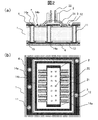
- FIG. 2A is a cross-sectional view of a component mounting board.
- FIG. 2B is a view of the printed circuit board 1 viewed from the mounting direction of the component (connector) 2.
- it is characterized in that it has a structure for preventing the penetration of the coating material on the mounting surface of the component (connector) 2.
- the silk (coating material permeation preventing member) 14a is provided in advance so as to be under the coating material 4 and to surround the component (connector) 2. Further, a varnish permeating silk (coating material permeation preventing member) 14b is provided in advance so as to surround the component (connector) 2 on the inner side closer to the component (connector) 2 than 14a. In other words, in the silk printing process, the silk 14b is printed between the region where the silk 14a is printed and the component, and so as to surround the component. At this time, the silk (coating material penetration preventing member) 14a performs the same function as that of the first embodiment. Therefore, the silk 14a is also installed directly under the component (connector) 2. Further, the holes of the through vias 11 that cannot be completely blocked by the resist 13 are closed by complementing the resist 13 with the silk 14a. Alternatively, the hole of the through via 11 is closed with the silk (coating material permeation prevention member) 14a alone.
- the silk (coating material permeation prevention member) 14a and the varnish permeation silk (coating material permeation prevention member) 14b described above have a permeation prevention area a having a groove structure in the silk printing thickness and the space between the silks. Constitute.
- the application of the coating material 4 on the mounting surface of the component (connector) 2 should avoid the application of the surrounding coating material 4 at a certain distance from the component (connector) 2 in consideration of the permeability of the coating material 4. Don't be.
- the above-described permeation prevention area a can be used as a boundary for applying the coating material 4.
- the coating material 4 applied on the silk (coating material permeation preventing member) 14a is in a state of liquid accumulation immediately after application, and tries to spread until the thickness, viscosity, surface tension, etc. of the coating material 4 are balanced. At this time, when the coating material 4 tries to penetrate into the component (connector) 2 around the component (connector) 2, the coating material 4 that has penetrated through the groove in the penetration prevention area a is stopped in place, and then to the component (connector) 2. Can be prevented.
- the permeation prevention area a by forming the permeation prevention area a, it is possible to arbitrarily set a range in which the surrounding coating material 4 applied at a certain distance from the component (connector) 2 is avoided. That is, since the penetration of the coating material 4 can be controlled, the application prohibited range of the coating material 4 can be minimized.
- Example 3 An application example of the printed circuit board in Example 3 will be described with reference to FIG. In the present embodiment, an example in which a component (connector) 2 having a different form is mounted on the printed circuit board 1 in the first embodiment will be described. Therefore, the description of the parts common to the first embodiment is omitted.
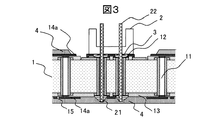
- FIG. 3 is an explanatory view showing a third embodiment of the component-mounting printed board to which the present invention is applied.
- the component (connector) 2 in the present embodiment is an insertion type, and the connection terminal 21 and the component terminal 22 of the component (connector) 2 are the same terminal.
- the component terminal 22 has exactly the same function as the connection terminal 22 in FIGS.
- the connection terminal 21 is a terminal to be inserted into the substrate, and is inserted into a component through hole having the same form as the through via 11.
- the component pad 12 in the component through hole is formed of a layer copper foil and a resist of the through hole.
- the present invention is not restricted by the mounting form of the component (connector) 2 mounted on the printed circuit board 1.
Landscapes
- Engineering & Computer Science (AREA)
- Manufacturing & Machinery (AREA)
- Microelectronics & Electronic Packaging (AREA)
- Non-Metallic Protective Coatings For Printed Circuits (AREA)
Abstract
La présente invention a pour but d'empêcher un matériau de revêtement d'adhérer à un terminal de composant par l'intermédiaire d'un trou d'interconnexion sans nécessiter, par rapport à une carte de circuit imprimé, une étape supplémentaire entre une étape de fabrication de carte imprimée et une étape de montage d'un composant sur la carte imprimée, et permet de réduire le coût d'application d'un matériau de revêtement empêchant la corrosion; la présente invention est caractérisée en ce qu'elle comprend : une étape de formation d'un trou d'interconnexion pénétrant une première surface et une seconde surface de la carte imprimée; et une étape d'impression par sérigraphie pour afficher des informations relatives à un composant sur la première surface ou la seconde surface. La présente invention est également caractérisée par la fermeture de l'ouverture du trou d'interconnexion lors de l'étape de sérigraphie.
Priority Applications (2)
| Application Number | Priority Date | Filing Date | Title |
|---|---|---|---|
| PCT/JP2016/059536 WO2017163390A1 (fr) | 2016-03-25 | 2016-03-25 | Carte de circuit imprimé et procédé de fabrication de carte de circuit imprimé |
| JP2018506720A JP6640986B2 (ja) | 2016-03-25 | 2016-03-25 | プリント基板及びプリント基板の製造方法 |
Applications Claiming Priority (1)
| Application Number | Priority Date | Filing Date | Title |
|---|---|---|---|
| PCT/JP2016/059536 WO2017163390A1 (fr) | 2016-03-25 | 2016-03-25 | Carte de circuit imprimé et procédé de fabrication de carte de circuit imprimé |
Publications (1)
| Publication Number | Publication Date |
|---|---|
| WO2017163390A1 true WO2017163390A1 (fr) | 2017-09-28 |
Family
ID=59901083
Family Applications (1)
| Application Number | Title | Priority Date | Filing Date |
|---|---|---|---|
| PCT/JP2016/059536 Ceased WO2017163390A1 (fr) | 2016-03-25 | 2016-03-25 | Carte de circuit imprimé et procédé de fabrication de carte de circuit imprimé |
Country Status (2)
| Country | Link |
|---|---|
| JP (1) | JP6640986B2 (fr) |
| WO (1) | WO2017163390A1 (fr) |
Citations (7)
| Publication number | Priority date | Publication date | Assignee | Title |
|---|---|---|---|---|
| JPS59189266U (ja) * | 1983-06-01 | 1984-12-15 | シャープ株式会社 | プリント基板 |
| JPS63131593A (ja) * | 1986-11-20 | 1988-06-03 | 日本電気株式会社 | 厚膜回路基板 |
| JPH0160571U (fr) * | 1987-10-12 | 1989-04-17 | ||
| JPH04343288A (ja) * | 1991-05-21 | 1992-11-30 | Sony Corp | プリント配線板 |
| JPH05110235A (ja) * | 1991-10-18 | 1993-04-30 | Nec Corp | コーテイング対応プリント配線板 |
| JPH06125164A (ja) * | 1992-10-12 | 1994-05-06 | Omron Corp | スルーホールプリント配線基板 |
| JP2004179576A (ja) * | 2002-11-29 | 2004-06-24 | Ngk Spark Plug Co Ltd | 配線基板及びその製造方法 |
Family Cites Families (4)
| Publication number | Priority date | Publication date | Assignee | Title |
|---|---|---|---|---|
| JPH04127670U (ja) * | 1991-05-10 | 1992-11-20 | ソニー株式会社 | 電子回路装置 |
| JPH1056246A (ja) * | 1996-08-12 | 1998-02-24 | Hitachi Telecom Technol Ltd | プリント配線板構造 |
| JP4383609B2 (ja) * | 1999-11-24 | 2009-12-16 | キヤノン株式会社 | プリント配線板 |
| JP2009188156A (ja) * | 2008-02-06 | 2009-08-20 | Canon Inc | プリント配線基板 |
-
2016
- 2016-03-25 WO PCT/JP2016/059536 patent/WO2017163390A1/fr not_active Ceased
- 2016-03-25 JP JP2018506720A patent/JP6640986B2/ja active Active
Patent Citations (7)
| Publication number | Priority date | Publication date | Assignee | Title |
|---|---|---|---|---|
| JPS59189266U (ja) * | 1983-06-01 | 1984-12-15 | シャープ株式会社 | プリント基板 |
| JPS63131593A (ja) * | 1986-11-20 | 1988-06-03 | 日本電気株式会社 | 厚膜回路基板 |
| JPH0160571U (fr) * | 1987-10-12 | 1989-04-17 | ||
| JPH04343288A (ja) * | 1991-05-21 | 1992-11-30 | Sony Corp | プリント配線板 |
| JPH05110235A (ja) * | 1991-10-18 | 1993-04-30 | Nec Corp | コーテイング対応プリント配線板 |
| JPH06125164A (ja) * | 1992-10-12 | 1994-05-06 | Omron Corp | スルーホールプリント配線基板 |
| JP2004179576A (ja) * | 2002-11-29 | 2004-06-24 | Ngk Spark Plug Co Ltd | 配線基板及びその製造方法 |
Also Published As
| Publication number | Publication date |
|---|---|
| JP6640986B2 (ja) | 2020-02-05 |
| JPWO2017163390A1 (ja) | 2018-09-13 |
Similar Documents
| Publication | Publication Date | Title |
|---|---|---|
| US7400511B2 (en) | Electronic component mounting structure | |
| KR20200003113A (ko) | Pcb, 패키지 구조체, 단말기 및 pcb 가공 방법 | |
| KR20110077042A (ko) | 인쇄회로기판조립체의 제조방법 | |
| JP2011254050A (ja) | プリント基板の製造方法 | |
| JP6640986B2 (ja) | プリント基板及びプリント基板の製造方法 | |
| US6667090B2 (en) | Coupon registration mechanism and method | |
| JP6909445B2 (ja) | 電子機器、電子機器の製造方法、プリント基板、プリント基板の製造方法 | |
| JP2015023040A (ja) | 基板構造 | |
| US20120292088A1 (en) | Electronic device with obliquely connected components | |
| JP2005327895A (ja) | プリント配線板 | |
| JP5067283B2 (ja) | 部品実装方法 | |
| JP6727115B2 (ja) | 電子制御装置の配線基板 | |
| CN105208775A (zh) | 一种防止bga焊接连锡的pcb设计方法 | |
| JP2015088531A (ja) | プリント基板の製造方法、プリント基板、及び表示装置 | |
| JP7455078B2 (ja) | プリント配線板 | |
| KR100584142B1 (ko) | 이동단말기용 월 인쇄회로기판과 칩셋 장치 | |
| JP2014165235A (ja) | 回路基板及び接続構造 | |
| JP5896522B2 (ja) | 封止部品に適した配線基板及びチップ部品並びにその製造方法 | |
| JP6779063B2 (ja) | プリント基板構造及びプリント基板の設計方法 | |
| JP2023058975A (ja) | プリント配線基板 | |
| JP2008103547A (ja) | 半田ペースト塗布方法及び電子回路基板 | |
| JP2008091557A (ja) | 電子部品の実装方法および実装装置 | |
| JPS63226994A (ja) | プリント配線板のソルダーレジスト用印刷インク | |
| JP6171898B2 (ja) | 電子装置及びその製造方法 | |
| JPH0534137Y2 (fr) |
Legal Events
| Date | Code | Title | Description |
|---|---|---|---|
| ENP | Entry into the national phase |
Ref document number: 2018506720 Country of ref document: JP Kind code of ref document: A |
|
| NENP | Non-entry into the national phase |
Ref country code: DE |
|
| 121 | Ep: the epo has been informed by wipo that ep was designated in this application |
Ref document number: 16895426 Country of ref document: EP Kind code of ref document: A1 |
|
| 122 | Ep: pct application non-entry in european phase |
Ref document number: 16895426 Country of ref document: EP Kind code of ref document: A1 |