WO2017169754A1 - Dispositif d'imagerie à semi-conducteurs et dispositif électronique - Google Patents
Dispositif d'imagerie à semi-conducteurs et dispositif électronique Download PDFInfo
- Publication number
- WO2017169754A1 WO2017169754A1 PCT/JP2017/010301 JP2017010301W WO2017169754A1 WO 2017169754 A1 WO2017169754 A1 WO 2017169754A1 JP 2017010301 W JP2017010301 W JP 2017010301W WO 2017169754 A1 WO2017169754 A1 WO 2017169754A1
- Authority
- WO
- WIPO (PCT)
- Prior art keywords
- pixel
- sensitivity
- photoelectric conversion
- conversion unit
- low
- Prior art date
- Legal status (The legal status is an assumption and is not a legal conclusion. Google has not performed a legal analysis and makes no representation as to the accuracy of the status listed.)
- Ceased
Links
Images



















Classifications
-
- H—ELECTRICITY
- H10—SEMICONDUCTOR DEVICES; ELECTRIC SOLID-STATE DEVICES NOT OTHERWISE PROVIDED FOR
- H10F—INORGANIC SEMICONDUCTOR DEVICES SENSITIVE TO INFRARED RADIATION, LIGHT, ELECTROMAGNETIC RADIATION OF SHORTER WAVELENGTH OR CORPUSCULAR RADIATION
- H10F39/00—Integrated devices, or assemblies of multiple devices, comprising at least one element covered by group H10F30/00, e.g. radiation detectors comprising photodiode arrays
- H10F39/80—Constructional details of image sensors
- H10F39/802—Geometry or disposition of elements in pixels, e.g. address-lines or gate electrodes
- H10F39/8027—Geometry of the photosensitive area
-
- H—ELECTRICITY
- H04—ELECTRIC COMMUNICATION TECHNIQUE
- H04N—PICTORIAL COMMUNICATION, e.g. TELEVISION
- H04N25/00—Circuitry of solid-state image sensors [SSIS]; Control thereof
- H04N25/50—Control of the SSIS exposure
- H04N25/57—Control of the dynamic range
- H04N25/58—Control of the dynamic range involving two or more exposures
- H04N25/581—Control of the dynamic range involving two or more exposures acquired simultaneously
- H04N25/585—Control of the dynamic range involving two or more exposures acquired simultaneously with pixels having different sensitivities within the sensor, e.g. fast or slow pixels or pixels having different sizes
-
- H—ELECTRICITY
- H04—ELECTRIC COMMUNICATION TECHNIQUE
- H04N—PICTORIAL COMMUNICATION, e.g. TELEVISION
- H04N25/00—Circuitry of solid-state image sensors [SSIS]; Control thereof
- H04N25/60—Noise processing, e.g. detecting, correcting, reducing or removing noise
- H04N25/62—Detection or reduction of noise due to excess charges produced by the exposure, e.g. smear, blooming, ghost image, crosstalk or leakage between pixels
- H04N25/621—Detection or reduction of noise due to excess charges produced by the exposure, e.g. smear, blooming, ghost image, crosstalk or leakage between pixels for the control of blooming
-
- H—ELECTRICITY
- H04—ELECTRIC COMMUNICATION TECHNIQUE
- H04N—PICTORIAL COMMUNICATION, e.g. TELEVISION
- H04N25/00—Circuitry of solid-state image sensors [SSIS]; Control thereof
- H04N25/70—SSIS architectures; Circuits associated therewith
-
- H—ELECTRICITY
- H10—SEMICONDUCTOR DEVICES; ELECTRIC SOLID-STATE DEVICES NOT OTHERWISE PROVIDED FOR
- H10F—INORGANIC SEMICONDUCTOR DEVICES SENSITIVE TO INFRARED RADIATION, LIGHT, ELECTROMAGNETIC RADIATION OF SHORTER WAVELENGTH OR CORPUSCULAR RADIATION
- H10F39/00—Integrated devices, or assemblies of multiple devices, comprising at least one element covered by group H10F30/00, e.g. radiation detectors comprising photodiode arrays
- H10F39/10—Integrated devices
- H10F39/12—Image sensors
- H10F39/199—Back-illuminated image sensors
-
- H—ELECTRICITY
- H10—SEMICONDUCTOR DEVICES; ELECTRIC SOLID-STATE DEVICES NOT OTHERWISE PROVIDED FOR
- H10F—INORGANIC SEMICONDUCTOR DEVICES SENSITIVE TO INFRARED RADIATION, LIGHT, ELECTROMAGNETIC RADIATION OF SHORTER WAVELENGTH OR CORPUSCULAR RADIATION
- H10F39/00—Integrated devices, or assemblies of multiple devices, comprising at least one element covered by group H10F30/00, e.g. radiation detectors comprising photodiode arrays
- H10F39/80—Constructional details of image sensors
- H10F39/802—Geometry or disposition of elements in pixels, e.g. address-lines or gate electrodes
- H10F39/8023—Disposition of the elements in pixels, e.g. smaller elements in the centre of the imager compared to larger elements at the periphery
-
- H—ELECTRICITY
- H10—SEMICONDUCTOR DEVICES; ELECTRIC SOLID-STATE DEVICES NOT OTHERWISE PROVIDED FOR
- H10F—INORGANIC SEMICONDUCTOR DEVICES SENSITIVE TO INFRARED RADIATION, LIGHT, ELECTROMAGNETIC RADIATION OF SHORTER WAVELENGTH OR CORPUSCULAR RADIATION
- H10F39/00—Integrated devices, or assemblies of multiple devices, comprising at least one element covered by group H10F30/00, e.g. radiation detectors comprising photodiode arrays
- H10F39/80—Constructional details of image sensors
- H10F39/803—Pixels having integrated switching, control, storage or amplification elements
-
- H—ELECTRICITY
- H10—SEMICONDUCTOR DEVICES; ELECTRIC SOLID-STATE DEVICES NOT OTHERWISE PROVIDED FOR
- H10F—INORGANIC SEMICONDUCTOR DEVICES SENSITIVE TO INFRARED RADIATION, LIGHT, ELECTROMAGNETIC RADIATION OF SHORTER WAVELENGTH OR CORPUSCULAR RADIATION
- H10F39/00—Integrated devices, or assemblies of multiple devices, comprising at least one element covered by group H10F30/00, e.g. radiation detectors comprising photodiode arrays
- H10F39/80—Constructional details of image sensors
- H10F39/803—Pixels having integrated switching, control, storage or amplification elements
- H10F39/8033—Photosensitive area
-
- H—ELECTRICITY
- H10—SEMICONDUCTOR DEVICES; ELECTRIC SOLID-STATE DEVICES NOT OTHERWISE PROVIDED FOR
- H10F—INORGANIC SEMICONDUCTOR DEVICES SENSITIVE TO INFRARED RADIATION, LIGHT, ELECTROMAGNETIC RADIATION OF SHORTER WAVELENGTH OR CORPUSCULAR RADIATION
- H10F39/00—Integrated devices, or assemblies of multiple devices, comprising at least one element covered by group H10F30/00, e.g. radiation detectors comprising photodiode arrays
- H10F39/80—Constructional details of image sensors
- H10F39/803—Pixels having integrated switching, control, storage or amplification elements
- H10F39/8037—Pixels having integrated switching, control, storage or amplification elements the integrated elements comprising a transistor
- H10F39/80373—Pixels having integrated switching, control, storage or amplification elements the integrated elements comprising a transistor characterised by the gate of the transistor
-
- H—ELECTRICITY
- H10—SEMICONDUCTOR DEVICES; ELECTRIC SOLID-STATE DEVICES NOT OTHERWISE PROVIDED FOR
- H10F—INORGANIC SEMICONDUCTOR DEVICES SENSITIVE TO INFRARED RADIATION, LIGHT, ELECTROMAGNETIC RADIATION OF SHORTER WAVELENGTH OR CORPUSCULAR RADIATION
- H10F39/00—Integrated devices, or assemblies of multiple devices, comprising at least one element covered by group H10F30/00, e.g. radiation detectors comprising photodiode arrays
- H10F39/80—Constructional details of image sensors
- H10F39/803—Pixels having integrated switching, control, storage or amplification elements
- H10F39/8037—Pixels having integrated switching, control, storage or amplification elements the integrated elements comprising a transistor
- H10F39/80377—Pixels having integrated switching, control, storage or amplification elements the integrated elements comprising a transistor characterised by the channel of the transistor, e.g. channel having a doping gradient
-
- H—ELECTRICITY
- H10—SEMICONDUCTOR DEVICES; ELECTRIC SOLID-STATE DEVICES NOT OTHERWISE PROVIDED FOR
- H10F—INORGANIC SEMICONDUCTOR DEVICES SENSITIVE TO INFRARED RADIATION, LIGHT, ELECTROMAGNETIC RADIATION OF SHORTER WAVELENGTH OR CORPUSCULAR RADIATION
- H10F39/00—Integrated devices, or assemblies of multiple devices, comprising at least one element covered by group H10F30/00, e.g. radiation detectors comprising photodiode arrays
- H10F39/80—Constructional details of image sensors
- H10F39/805—Coatings
- H10F39/8057—Optical shielding
-
- H—ELECTRICITY
- H10—SEMICONDUCTOR DEVICES; ELECTRIC SOLID-STATE DEVICES NOT OTHERWISE PROVIDED FOR
- H10F—INORGANIC SEMICONDUCTOR DEVICES SENSITIVE TO INFRARED RADIATION, LIGHT, ELECTROMAGNETIC RADIATION OF SHORTER WAVELENGTH OR CORPUSCULAR RADIATION
- H10F39/00—Integrated devices, or assemblies of multiple devices, comprising at least one element covered by group H10F30/00, e.g. radiation detectors comprising photodiode arrays
- H10F39/80—Constructional details of image sensors
- H10F39/806—Optical elements or arrangements associated with the image sensors
- H10F39/8063—Microlenses
-
- H—ELECTRICITY
- H10—SEMICONDUCTOR DEVICES; ELECTRIC SOLID-STATE DEVICES NOT OTHERWISE PROVIDED FOR
- H10F—INORGANIC SEMICONDUCTOR DEVICES SENSITIVE TO INFRARED RADIATION, LIGHT, ELECTROMAGNETIC RADIATION OF SHORTER WAVELENGTH OR CORPUSCULAR RADIATION
- H10F39/00—Integrated devices, or assemblies of multiple devices, comprising at least one element covered by group H10F30/00, e.g. radiation detectors comprising photodiode arrays
- H10F39/80—Constructional details of image sensors
- H10F39/807—Pixel isolation structures
-
- H—ELECTRICITY
- H10—SEMICONDUCTOR DEVICES; ELECTRIC SOLID-STATE DEVICES NOT OTHERWISE PROVIDED FOR
- H10F—INORGANIC SEMICONDUCTOR DEVICES SENSITIVE TO INFRARED RADIATION, LIGHT, ELECTROMAGNETIC RADIATION OF SHORTER WAVELENGTH OR CORPUSCULAR RADIATION
- H10F39/00—Integrated devices, or assemblies of multiple devices, comprising at least one element covered by group H10F30/00, e.g. radiation detectors comprising photodiode arrays
- H10F39/80—Constructional details of image sensors
- H10F39/812—Arrangements for transferring the charges in the image sensor perpendicular to the imaging plane, e.g. buried regions used to transfer generated charges to circuitry under the photosensitive region
-
- H—ELECTRICITY
- H10—SEMICONDUCTOR DEVICES; ELECTRIC SOLID-STATE DEVICES NOT OTHERWISE PROVIDED FOR
- H10F—INORGANIC SEMICONDUCTOR DEVICES SENSITIVE TO INFRARED RADIATION, LIGHT, ELECTROMAGNETIC RADIATION OF SHORTER WAVELENGTH OR CORPUSCULAR RADIATION
- H10F39/00—Integrated devices, or assemblies of multiple devices, comprising at least one element covered by group H10F30/00, e.g. radiation detectors comprising photodiode arrays
- H10F39/80—Constructional details of image sensors
- H10F39/813—Electronic components shared by multiple pixels, e.g. one amplifier shared by two pixels
-
- H—ELECTRICITY
- H10—SEMICONDUCTOR DEVICES; ELECTRIC SOLID-STATE DEVICES NOT OTHERWISE PROVIDED FOR
- H10F—INORGANIC SEMICONDUCTOR DEVICES SENSITIVE TO INFRARED RADIATION, LIGHT, ELECTROMAGNETIC RADIATION OF SHORTER WAVELENGTH OR CORPUSCULAR RADIATION
- H10F39/00—Integrated devices, or assemblies of multiple devices, comprising at least one element covered by group H10F30/00, e.g. radiation detectors comprising photodiode arrays
- H10F39/10—Integrated devices
- H10F39/12—Image sensors
- H10F39/18—Complementary metal-oxide-semiconductor [CMOS] image sensors; Photodiode array image sensors
- H10F39/182—Colour image sensors
Definitions
- the present technology relates to a solid-state imaging device and an electronic device, and more particularly to a solid-state imaging device and an electronic device that can further expand a dynamic range in a pixel having a high sensitivity pixel and a low sensitivity pixel.
- Solid-state imaging devices such as CMOS (Complementary Metal Oxide Semiconductor) image sensors are used in electronic devices such as imaging devices such as digital still cameras and video cameras, and portable terminal devices having an imaging function.
- CMOS Complementary Metal Oxide Semiconductor
- the sensitivity is high so that an imaging signal can be acquired even at low illumination.
- the dynamic range becomes large, it is desirable that the photodiode is less likely to be saturated.
- the high sensitivity and the difficulty of saturating the photodiode are in a trade-off relationship, and it is difficult to expand the dynamic range while maintaining the sensitivity.
- CMOS image sensor that includes both high-sensitivity pixels and low-sensitivity pixels, and that maintains high sensitivity with high-sensitivity pixels and expands the dynamic range with low-sensitivity pixels has been proposed (see, for example, Patent Document 1). ).
- the present technology has been made in view of such a situation, and enables a dynamic range to be further expanded in a pixel having a high sensitivity pixel and a low sensitivity pixel.
- the solid-state imaging device includes a pixel array unit in which a plurality of pixels are two-dimensionally arranged, and the pixels include a first photoelectric conversion unit and the first photoelectric conversion unit.
- a second photoelectric conversion unit having a lower sensitivity than the first photoelectric conversion unit.
- the second photoelectric conversion unit has a size in the optical axis direction where light is incident larger than a size in the optical axis direction of the first photoelectric conversion unit. This is a solid-state imaging device having a small size.
- the solid-state imaging device includes a pixel array unit in which a plurality of pixels are two-dimensionally arranged, and the pixels include a first photoelectric conversion unit and the first photoelectric conversion unit.
- a second photoelectric conversion unit having a lower sensitivity than the first photoelectric conversion unit.
- the second photoelectric conversion unit has a size in the optical axis direction where light is incident larger than a size in the optical axis direction of the first photoelectric conversion unit.
- a solid-state imaging device includes a pixel array unit in which a plurality of pixels are two-dimensionally arranged, and the pixels include a first photoelectric conversion unit and the first photoelectric conversion unit.
- a second photoelectric conversion unit having a lower sensitivity than the first photoelectric conversion unit, and a pixel internal capacitor that accumulates charges overflowed by the second photoelectric conversion unit, and the second photoelectric conversion unit has an optical axis on which light is incident.
- the size in the direction is smaller than the size in the optical axis direction of the first photoelectric conversion unit, and the second photoelectric conversion unit and the pixel internal capacitance are the light incident side of the second photoelectric conversion unit.
- a solid-state imaging device in which the region of the first photoelectric conversion unit is expanded to a region that can be secured by forming a stacked structure of the second photoelectric conversion unit and the pixel capacitance. is there.
- a solid-state imaging device includes a pixel array unit in which a plurality of pixels are two-dimensionally arranged, and the pixels include a first photoelectric conversion unit and the first photoelectric conversion unit. And a second photoelectric conversion unit having a lower sensitivity than the first photoelectric conversion unit, and a fine uneven structure is formed on the light incident side of the first photoelectric conversion unit.
- a solid-state imaging device includes a pixel array unit in which a plurality of pixels are two-dimensionally arranged, and the pixels include a first photoelectric conversion unit and the first photoelectric conversion unit.
- a second photoelectric conversion unit having a lower sensitivity than the first photoelectric conversion unit.
- the second photoelectric conversion unit is a solid-state imaging device formed so as to surround the first photoelectric conversion unit.
- An electronic apparatus includes a pixel array unit in which a plurality of pixels are two-dimensionally arranged, and the pixels include a first photoelectric conversion unit and the first photoelectric conversion unit.
- a second photoelectric conversion unit having a lower sensitivity than the first photoelectric conversion unit.
- the second photoelectric conversion unit has a size in the optical axis direction where light is incident larger than a size in the optical axis direction of the first photoelectric conversion unit. It is an electronic device including a solid-state imaging device having a small size.
- the dynamic range can be further expanded in the pixel having the high sensitivity pixel and the low sensitivity pixel.
- FIG. 1 is a diagram illustrating an embodiment of a solid-state imaging device to which the present technology is applied.
- the CMOS image sensor 10 in FIG. 1 is a solid-state imaging device using CMOS (Complementary Metal Metal Oxide Semiconductor).
- CMOS Complementary Metal Metal Oxide Semiconductor
- the CMOS image sensor 10 takes in incident light (image light) from a subject via an optical lens system (not shown), and converts the amount of incident light imaged on the imaging surface into an electrical signal in units of pixels. Output as a pixel signal.
- a CMOS image sensor 10 includes a pixel array unit 11, a vertical drive circuit 12, a column signal processing circuit 13, a horizontal drive circuit 14, an output circuit 15, a control circuit 16, and an input / output terminal 17. .
- a plurality of pixels 100 are two-dimensionally arranged in the pixel array unit 11.
- the pixel 100 includes a photodiode as a photoelectric conversion element and a plurality of pixel transistors.
- the vertical drive circuit 12 includes, for example, a shift register, selects a predetermined pixel drive line 21, supplies a pulse for driving the pixel 100 to the selected pixel drive line 21, and sets the pixels 100 in units of rows. To drive. That is, the vertical driving circuit 12 sequentially selects and scans each pixel 100 of the pixel array unit 11 in the vertical direction in units of rows, and outputs a pixel signal based on a signal charge generated according to the amount of received light in the photodiode of each pixel 100. , And supplied to the column signal processing circuit 13 through the vertical signal line 22.
- the column signal processing circuit 13 is arranged for each column of the pixels 100, and performs signal processing such as noise removal on the signal output from the pixels 100 for one row for each pixel column.
- the column signal processing circuit 13 performs signal processing such as CDS (Correlated Double Sampling) and A / D (Analog / Digital) conversion for removing fixed pattern noise unique to a pixel.
- the horizontal drive circuit 14 is constituted by, for example, a shift register, and sequentially outputs horizontal scanning pulses to sequentially select each of the column signal processing circuits 13, and outputs a pixel signal from each of the column signal processing circuits 13 to the horizontal signal line. 23 to output.
- the output circuit 15 performs signal processing on the signals sequentially supplied from each of the column signal processing circuits 13 through the horizontal signal line 23 and outputs the signals.
- the output circuit 15 may perform only buffering, for example, or may perform black level adjustment, column variation correction, various digital signal processing, and the like.
- the control circuit 16 controls the operation of each part of the CMOS image sensor 10.
- the control circuit 16 receives an input clock signal and data for instructing an operation mode and outputs data such as internal information of the CMOS image sensor 10. That is, the control circuit 16 uses the vertical synchronization signal, the horizontal synchronization signal, and the master clock signal as a reference for the operation of the vertical drive circuit 12, the column signal processing circuit 13, the horizontal drive circuit 14, and the like. And generate control signals.
- the control circuit 16 outputs the generated clock signal and control signal to the vertical drive circuit 12, the column signal processing circuit 13, the horizontal drive circuit 14, and the like.
- the input / output terminal 17 exchanges signals with the outside.
- the CMOS image sensor 10 of FIG. 1 configured as described above is a CMOS image sensor called a column AD system in which column signal processing circuits 13 that perform CDS processing and A / D conversion processing are arranged for each pixel column.
- the CMOS image sensor 10 of FIG. 1 can be a back-illuminated CMOS image sensor.
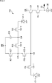
- FIG. 2 is a diagram illustrating a circuit configuration example of the pixel 100 of FIG.
- the pixel 100 includes a high-sensitivity photodiode 121-1, a low-sensitivity photodiode 121-1, a first transfer transistor 122-1, a second transfer transistor 122-2, a third transfer transistor 122-3, and a fourth transfer transistor 122-. 4, a charge storage unit 123, an FD (Floating Diffusion) unit 126, a reset transistor 127, an amplification transistor 128, and a selection transistor 129.
- FD Floating Diffusion
- a plurality of drive lines are wired to the pixels 100 as pixel drive lines 21 (FIG. 1), for example, for each pixel row.
- Various drive signals TGL, TGS, FCG, FDG, RST, and SEL are supplied through a plurality of drive lines from the vertical drive circuit 12 (FIG. 1). These drive signals are pulses in which each transistor of the pixel 100 is an NMOS transistor, so that a high level (for example, power supply VDD) state is active and a low level (for example, negative potential) is inactive. Signal.
- the high-sensitivity photodiode 121-1 is, for example, a photoelectric conversion unit including a PN junction photodiode (PD).
- the high-sensitivity photodiode 121-1 generates and accumulates charges according to the received light quantity.
- the low sensitivity photodiode 121-2 is, for example, a photoelectric conversion unit made of a PN junction photodiode (PD).
- the low-sensitivity photodiode 121-2 generates and accumulates charges corresponding to the received light quantity.
- the high-sensitivity photodiode 121-1 when comparing the high-sensitivity photodiode 121-1 and the low-sensitivity photodiode 121-2, the high-sensitivity photodiode 121-1 has a unit illuminance per unit time than the low-sensitivity photodiode 121-2. The total amount of charges (signal charges) generated per hit increases. Therefore, the high sensitivity photodiode 121-1 has higher sensitivity, and the low sensitivity photodiode 121-2 has lower sensitivity.
- the first transfer transistor 122-1 is connected between the high sensitivity photodiode 121-1 and the FD unit 126.
- a drive signal TGL is applied to the gate electrode of the first transfer transistor 122-1.
- this drive signal TGL becomes active, the transfer gate of the first transfer transistor 122-1 becomes conductive, and the charge accumulated in the high sensitivity photodiode 121-1 passes through the first transfer transistor 122-1. Transferred to the FD unit 126.
- the second transfer transistor 122-2 is connected between the FD unit 124 and the FD unit 125.
- the drive signal FCG is applied to the gate electrode of the second transfer transistor 122-2.
- the transfer gate of the second transfer transistor 122-2 becomes conductive, and the potentials of the FD portion 124 and the FD portion 125 are coupled.
- the third transfer transistor 122-3 is connected between the low sensitivity photodiode 121-2 and the FD unit 124.
- the drive signal TGS is applied to the gate electrode of the third transfer transistor 122-3.
- the transfer gate of the third transfer transistor 122-3 becomes conductive, and the charge accumulated in the low sensitivity photodiode 121-2 passes through the third transfer transistor 122-3. Then, it is transferred to a region where the potentials of the charge storage unit 123 or the FD unit 124 and the FD unit 125 are combined.
- the fourth transfer transistor 122-4 is connected between the FD unit 125 and the FD unit 126 between the second transfer transistor 122-2, the fourth transfer transistor 122-4, and the reset transistor 127.
- the drive signal FDG is applied to the gate electrode of the fourth transfer transistor 122-4.
- the transfer gate of the fourth transfer transistor 122-4 becomes conductive, and the FD portion 125 between the second transfer transistor 122-2, the reset transistor 127, and the fourth transfer transistor 122-4.
- the potential of the FD portion 126 are combined.
- the charge storage unit 123 includes a capacitor and is connected to the FD unit 124 between the second transfer transistor 122-2 and the third transfer transistor 122-3.
- the counter electrode of the charge storage unit 123 is connected between the power supply VDD that supplies the power supply VDD.
- the charge storage unit 123 stores the charge transferred or overflowed from the low sensitivity photodiode 121-2.
- the charge storage unit 123 corresponds to a pixel internal capacity (FC: Floating Capacitor) (for example, the internal capacity 123 in FIG. 10) described later.
- the FD unit 126 is FD (Floating Diffusion), and converts the charge into a voltage signal and outputs it.
- the FD unit 126 corresponds to “FD1” in a plan view (for example, a plan view of A in FIG. 6) described later.
- the FD unit 125 corresponds to “FD2” in a plan view described later, and the FD unit 124 corresponds to “FD3” in a plan view described later.
- the reset transistor 127 is connected between the power supply VDD and the FD unit 125.
- a drive signal RST and a drive signal FDG are applied to the gate electrode of the reset transistor 127.
- this drive signal RST becomes active, the reset gate of the reset transistor 127 becomes conductive, and the potential of the FD portion 126 is reset to the level of the power supply VDD.
- the amplification transistor 128 has a gate electrode connected to the FD unit 126, a drain electrode connected to the power supply VDD, and a read circuit that reads a voltage signal held in the FD unit 126, that is, an input unit of a so-called source follower circuit.
- the amplifying transistor 128 has a source electrode connected to the vertical signal line 22 (FIG. 1) via the selection transistor 129, whereby a constant current source 130 and a source follower connected to one end of the vertical signal line 22 are connected. Configure the circuit.
- the selection transistor 129 is connected between the source electrode of the amplification transistor 128 and the vertical signal line 22.
- a drive signal SEL is applied to the gate electrode of the selection transistor 129.
- the selection transistor 129 becomes conductive and the pixel 100 becomes selected.
- the pixel signal output from the amplification transistor 128 is output to the vertical signal line 22 (FIG. 1) via the selection transistor 129.
- the pixel 100 is configured as described above.
- the high-sensitivity imaging unit including the transfer transistor that transfers the charge generated at ⁇ 1 is also referred to as “high-sensitivity pixel (high-sensitivity pixel unit)”.
- the low-sensitivity photodiode 121-2 included in the pixel 100 of FIG. 2 an on-chip lens for making light incident on the low-sensitivity photodiode 121-2, and the charge generated by the low-sensitivity photodiode 121-2.
- the low-sensitivity image pickup unit including the transfer transistor that transfers the signal is also referred to as “low-sensitivity pixel (low-sensitivity pixel unit)”.
- the charge storage unit 123 is provided so that the charge overflowed by the low-sensitivity photodiode 121-2 can be stored, but a configuration in which the charge storage unit 123 is not provided is employed. You can also Therefore, in the embodiment described later, there are both a structure in which the charge storage unit 123 is provided and a structure in which the charge storage unit 123 is not provided for the low sensitivity photodiode 121-2. .
- the CMOS image sensor 10 can expand the dynamic range by using the different sensitivity between the high-sensitivity pixel having the high-sensitivity photodiode 121-1 and the low-sensitivity pixel having the low-sensitivity photodiode 121-2.
- a plurality of configurations can be adopted. Therefore, hereinafter, first to sixth embodiments corresponding to the configuration of a plurality of pixels 100 arranged two-dimensionally in the pixel array unit 11 of the CMOS image sensor 10 will be described.
- the pixel of the first embodiment is described as a pixel 900, and is distinguished from the pixels of other embodiments.
- the pixels of the second to sixth embodiments are described as a pixel 100, a pixel 200, a pixel 300, a pixel 400, and a pixel 500, respectively.
- These pixels are also referred to as the CMOS image sensor 10 ( The two-dimensional arrangement in the pixel array section 11 of FIG.
- the pixel 900 is provided as the pixel 100 arranged two-dimensionally in the pixel array unit 11 of the CMOS image sensor 10 (FIG. 1).
- FIG. 3 is a plan view showing the structure of the pixel 900 according to the first embodiment.
- FIG. 3 shows a plan view when one of the pixels 900 arranged two-dimensionally in the pixel array section 11 of the back-illuminated CMOS image sensor 10 (FIG. 1) is viewed from the wiring side.
- the pixel 900 illustrated in FIG. 3 has a configuration similar to that of the pixel 100 illustrated in FIG.
- the pixel 900 includes a high sensitivity photodiode 921-1 and a low sensitivity photodiode 921-2.
- the first transfer transistor 922-1 to the selection transistor 929 correspond to the first transfer transistor 122-1 to the selection transistor 129 of the pixel 100 in FIG.
- a pixel internal capacitance (FC: Floating Capacitor) 923 corresponds to the charge accumulation unit 123 of the pixel 100 in FIG.
- a MOS capacitor can be used as an example of the in-pixel capacitor 923.
- FIG. 4 a high-sensitivity photodiode (PD) 921-1 and a low-sensitivity photodiode (PD) 921-2 are formed in a semiconductor substrate 912.
- the high-sensitivity photodiode 921-1 generates and accumulates charges corresponding to the amount of light incident through the on-chip lens 911-1.
- the charge accumulated in the high sensitivity photodiode 921-1 is read out by the pixel circuit. That is, the on-chip lens 911-1, the high-sensitivity photodiode 921-1, and the pixel circuit constitute a high-sensitivity pixel 901-1.
- the low-sensitivity photodiode 921-2 generates and accumulates charges corresponding to the amount of light incident through the on-chip lens 911-2.
- the charge accumulated in the low sensitivity photodiode 921-2 is read out by the pixel circuit. That is, the low-sensitivity pixel 901-2 is configured by the on-chip lens 911-2, the low-sensitivity photodiode 921-2, and the pixel circuit.
- the silicon (Si) depth direction of the semiconductor substrate 912 of the high-sensitivity photodiode 921-1 and the low-sensitivity photodiode 921-2 is equivalent, the size in the plane direction (area of the light receiving surface) is different.
- the planar size (light receiving surface area) of the low sensitivity photodiode 921-2 is smaller than the planar size (light receiving surface area) of the high sensitivity photodiode 921-1.
- the amount of charge generated as a result of photoelectric conversion is approximately proportional to the size (thickness) in the depth direction of the photodiode.
- the amount of charge generated as a result of photoelectric conversion in the photodiode is approximately proportional to the area of the light receiving surface of the photodiode.
- the high-sensitivity photodiode 921-1 and the low-sensitivity photodiode 921-2 have the same size (thickness) in the depth direction of the photodiode. Therefore, the amount of charge (signal charge) generated per unit area of the photodiode under the unit time and unit illuminance is equal between the high sensitivity photodiode 921-1 and the low sensitivity photodiode 921-2. .
- the size of the photodiode in the planar direction is smaller in the low sensitivity photodiode 921-2 than in the high sensitivity photodiode 921-1.
- the total amount of charge (signal charge) generated in the photodiode is smaller in the low-sensitivity photodiode 921-2 than in the high-sensitivity photodiode 921-1. More specifically, it decreases in proportion to the area of the light receiving surface of the photodiode.
- the high sensitivity photodiode 921-1 and the low sensitivity photodiode 921-2 have different sensitivities, and the sensitivity of the low sensitivity photodiode 921-2 is lower than that of the high sensitivity photodiode 921-1.
- the saturation charge amount (Qs) of the photodiode is approximately proportional to the size of the photodiode in the planar direction (the area of the light receiving surface). Since both the amount of charge generated as a result of photoelectric conversion in the photodiode and the saturation charge amount (Qs) of the photodiode are approximately proportional to the area of the light receiving surface of the photodiode, the high sensitivity photodiode 921-1 and the low sensitivity If both the photodiodes 921-2 are irradiated with light having the same illuminance and the illuminance is increased, the high sensitivity photodiode 921-1 and the low sensitivity photodiode 921-2 are saturated at the same illuminance. . That is, at the same illuminance, the amount of charge generated in each photodiode has reached the saturation charge amount (Qs) of each photodiode.
- the low-sensitivity photodiode 921-2 causes the charge generated as a result of photoelectric conversion to exceed the saturation charge amount (Qs) of the low-sensitivity photodiode 921-2.
- the charge generated according to the illuminance can be overflowed and accumulated in the pixel capacitor 923 and output as a signal charge.
- the high sensitivity photodiode 921-1 generates a high sensitivity photodiode.
- Overflow to the P-well layer which is a P-type impurity region around 921-1. As described above, the charge overflowed to the P well layer is absorbed by the drain region of the NMOS transistor included in the pixel 900 having the same structure as the pixel 100 shown in FIG. 2, and is not used as the signal charge.
- a low-sensitivity pixel portion (low-sensitivity pixel 901-2) including a pixel internal capacitance 923 and a low-sensitivity photodiode 921-2, and a high-sensitivity pixel portion (high-sensitivity pixel) including a high-sensitivity photodiode 921-1.
- 901-1) represents input / output characteristics.
- the horizontal axis represents the illuminance of light applied to each photodiode, and the vertical axis represents the amount of charge output from each photodiode.
- the dotted line in the figure represents the input / output characteristics of the high-sensitivity pixel portion (high-sensitivity pixel 901-1), and the alternate long and short dash line in the figure represents the input-output characteristics of the low-sensitivity pixel portion (low-sensitivity pixel 901-2). Represents.
- the low-sensitivity pixel unit In the high-sensitivity pixel portion, at a lower illuminance than the low-sensitivity pixel portion, the charge generated as a result of photoelectric conversion reaches the saturation charge amount (Qs), and the output is saturated.
- the low-sensitivity pixel unit outputs a signal charge corresponding to the illuminance even in the illuminance where the output of the high-sensitivity pixel unit is saturated. That is, in the input / output characteristics shown in FIG. 5, the low sensitivity pixel unit has a wider input range (illuminance range in which an output corresponding to the illuminance can be obtained) than the high sensitivity pixel unit, and the output range ( The range of the output charge amount) is widened. In other words, it can be said that the low sensitivity pixel unit has a wider dynamic range than the high sensitivity pixel unit.
- the CMOS image sensor 10 including the pixel 900 includes an amplifier that multiplies the output of the low-sensitivity pixel unit.
- the column signal processing circuit 13 shown in FIG. 1 includes this amplifier. The operation of this amplifier will be described below with reference to FIG.
- the high-sensitivity pixel portion has higher sensitivity than the low-sensitivity pixel in the illuminance region where the output is not saturated. For this reason, in FIG. 5 (inside the dotted line of “sensitivity ratio”), in the illuminance region where the output (dotted line) of the high-sensitivity pixel unit is not saturated, the inclination is the output of the low-sensitivity pixel unit (dashed line) It is larger than the slope. In other words, in this illuminance region, the output of the high-sensitivity pixel unit is larger than the output of the low-sensitivity pixel unit, and of course, the S / N ratio (SignalSignNoise ratio, hereinafter referred to as S / N) is also large. Get higher.
- FIG. 5 (outside the dotted line of “sensitivity ratio”), in the region where the output of the high-sensitivity pixel portion is saturated, an output corresponding to the illuminance is obtained from the low-sensitivity pixel portion. It becomes smaller than the slope of the output before the pixel portion is saturated. Therefore, in the CMOS image sensor 10 (FIG. 1) including the pixels 900, the amplifier (for example, the amplifier included in the column signal processing circuit 13 in FIG. 1) described above is used for the output obtained from the low sensitivity pixel unit. Try to multiply the gain.
- the amplifier for example, the amplifier included in the column signal processing circuit 13 in FIG.
- the slope of the output of the high-sensitivity pixel unit before saturation is the same as the slope of the output after gain increase, which is obtained by multiplying the output of the low-sensitivity pixel unit before saturation by a gain.
- a gain is applied to the output of the low-sensitivity pixel unit.
- the solid line in FIG. 5 represents the output of the low-sensitivity pixel unit after this gain increase (arrows A1 and A2 in the figure).
- the input irradiates the photodiode from the illuminance range where the high sensitivity pixel unit outputs the electric charge according to the illuminance to the illuminance range where the low sensitivity pixel unit outputs the electric charge according to the illuminance.
- a linear output (amount of charge output from the photodiode) can be obtained with respect to (illuminance of light).
- the output before saturation of the high-sensitivity pixel portion indicated by the dotted line in FIG. 5 has an S / N ratio higher than the output before saturation of the low-sensitivity pixel portion indicated by the one-dot chain line in FIG. Get higher.
- the output of the low sensitivity pixel unit has a lower S / N ratio than the output of the high sensitivity pixel unit.
- the CMOS image sensor 10 (FIG. 1) including the pixels 900 has data based on the output of the high-sensitivity pixel unit in the illuminance range in which the high-sensitivity pixel unit in FIG. 5 outputs charges according to the illuminance.
- data based on the output of the low-sensitivity pixel unit after gain increase can be output as pixel data of the imaging result.
- the CMOS image sensor 10 (FIG. 1) including the pixels 900 has a wider dynamic range in the direction of higher illuminance than that of the prior art, and can obtain characteristics with good S / N in the low illuminance region. it can.
- the CMOS image sensor 10 (FIG. 1) including the pixel 900 has a low-sensitivity pixel that does not apply gain without providing an amplifier that applies gain to the low-sensitivity pixel unit.
- Data based on the output of the unit may be output as pixel data of the imaging result. In this case, it is desirable to multiply the data based on the output of the low sensitivity pixel unit by a gain on the device side that receives the output of the CMOS image sensor 10.
- Second Embodiment Structure in which the size in the depth direction of a low-sensitivity PD is limited>
- the size in the planar direction of the low-sensitivity photodiode of the low-sensitivity pixel is formed to be smaller than the size in the planar direction of the high-sensitivity photodiode of the high-sensitivity pixel.
- the size of the low-sensitivity photodiode in the low-sensitivity pixel is limited in the depth direction to reduce the amount of charge generated as a result of photoelectric conversion.
- the size in the planar direction of the low-sensitivity photodiode of the low-sensitivity pixel can be made equal to or larger than the size in the planar direction of the high-sensitivity photodiode.
- the pixels 100A to 100D are described as the pixels 100 arranged two-dimensionally in the pixel array unit 11 of the CMOS image sensor 10 (FIG. 1).
- the pixels 100A and 100B are described.
- the pixel 100C and the pixel 100D have a structure having the pixel capacity 123, while the structure does not have the pixel capacity 123. Therefore, the pixel circuits of the pixel 100C and the pixel 100D correspond to the configuration of the pixel circuit shown in FIG. 2, but the pixel circuits of the pixel 100A and the pixel 100B are the pixel internal capacitance 123 in the pixel circuit shown in FIG. This corresponds to a configuration in which no is provided.
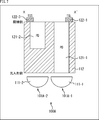
- the pixel 100A having a structure in which the size of the low-sensitivity photodiode (PD) in the depth direction is limited will be described with reference to the plan view of FIG. 6 and the cross-sectional view of FIG.
- FIG. 6 is a plan view showing the structure of the pixel 100A.
- a in FIG. 6 represents a plan view when one of the pixels 100A arranged two-dimensionally in the pixel array unit 11 of the CMOS image sensor 10 (FIG. 1) is viewed from the wiring side.
- B of FIG. 6 represents a plan view when the pixel 100A is viewed from the light incident side.
- FIG. 7 a high sensitivity photodiode (PD) 121-1 and a low sensitivity photodiode (PD) 121-2 are formed in silicon (Si) of a semiconductor substrate 112.
- the first transfer transistor 122-1 and the third transfer transistor 122-3 which will be described later, are also shown for convenience.
- the high-sensitivity photodiode 121-1 generates and accumulates electric charges according to the amount of light incident through the on-chip lens 111-1. Then, the charge accumulated in the high-sensitivity photodiode 121-1 is read out by the first transfer transistor 122-1 operating in accordance with the drive signal TGL applied to the gate electrode.
- a high-sensitivity pixel 101A-1 is configured by a pixel circuit such as the above.
- the low-sensitivity photodiode 121-2 generates and accumulates charges corresponding to the amount of light incident through the on-chip lens 111-2.
- the charge accumulated in the low-sensitivity photodiode 121-2 is read out by the third transfer transistor 122-3 operating according to the drive signal TGS applied to the gate electrode.
- a low-sensitivity pixel 101A-2 is configured by a pixel circuit such as the above.
- the size (area of the light receiving surface) in the planar direction of the high-sensitivity photodiode 121-1 and the low-sensitivity photodiode 121-2 is: Although the sizes are the same (substantially the same), the size of the semiconductor substrate 112 in the depth direction of silicon (Si) is different. Specifically, the size of the low sensitivity photodiode 121-2 in the depth direction is smaller than the size of the high sensitivity photodiode 121-1 in the depth direction.
- the size of the low sensitivity photodiode 121-2 is limited, and the high sensitivity photodiode 121 is limited.
- the size in the depth direction is made smaller than -1. Further, in this case, as shown in the plan view of the wiring side of FIG. 6A and the light incident side of FIG. 6B, the high-sensitivity photodiode 121-1 and the low-sensitivity photodiode 121-2 in the planar direction.
- the size (area of the light receiving surface) is the same (substantially the same) size.
- the pixel 100A of the second embodiment shown in FIGS. 6 and 7 is compared with the pixel 900 of the first embodiment shown in FIGS.
- the pixel 900 shown in FIG. 3 and FIG. 4 has a planar size (light receiving surface area) of the low sensitivity photodiode 921-2 and a planar size (light receiving surface area) of the high sensitivity photodiode 921-1.
- the amount of charge generated as a result of photoelectric conversion in the low-sensitivity photodiode 921-2 is made smaller than the amount of charge generated as a result of photoelectric conversion in the high-sensitivity photodiode 921-1.
- the low-sensitivity photodiode 921-2 includes an in-pixel capacitor 923 as charge storage means other than the low-sensitivity photodiode 921-2 in order to accumulate more charge generated as a result of photoelectric conversion.
- the low-sensitivity pixel of the pixel 900 including the low-sensitivity photodiode 921-2 and the pixel capacitance 923 can be stored.
- the unit (low-sensitivity pixel 901-2) accumulates electric charges according to the illuminance and outputs it without saturating the output over a wide illuminance range.
- the pixel 900 according to the first embodiment shown in FIGS. 3 and 4 can obtain characteristics with a wider dynamic range than the conventional technique.
- the size (thickness) of the low sensitivity photodiode 121-2 in the depth direction is the same as the size (thickness) of the high sensitivity photodiode 121-1.
- the amount of charge generated as a result of photoelectric conversion in the low-sensitivity photodiode 121-2 is made smaller than the amount of charge generated as a result of photoelectric conversion in the high-sensitivity photodiode 121-1.
- the size of the low-sensitivity photodiode 121-2 in the plane direction (the area of the light receiving surface) is set in the pixel 900.
- the saturation charge amount (Qs) of the low-sensitivity photodiode 121-2 is increased by making it larger than the size (area of the light-receiving surface) of the low-sensitivity photodiode 921-2 provided.
- the low-sensitivity pixel portion (low-sensitivity pixel) of the pixel 100A including the low-sensitivity photodiode 121-2. 101A-2) can accumulate and output charges according to the illuminance without saturating the output over a wide illuminance range.
- the pixel 100A of the second embodiment shown in FIGS. 6 and 7 can obtain characteristics with a wider dynamic range than the prior art.
- the pixel 100A accumulates the charge generated in the low sensitivity photodiode 121-2 in the photodiode.
- the photodiode stores charge in a potential well generated in the depleted photodiode, while the MOS capacitor has free electrons. Charges are accumulated using a large number of metals or degenerate semiconductors as electrodes. For this reason, it is less noise to store charges in a photodiode than to store charges in a MOS capacitor.
- the pixel 100A has the structure shown in FIGS. 6 and 7, so that a higher S / N can be obtained at the output of the low-sensitivity photodiode than the pixel 900 shown in FIGS. it can.
- the CMOS image sensor 10 (FIG. 1) including the pixel 100A has a wider dynamic range in the direction of higher illuminance than that of the prior art, and has a good S / N in both low illuminance and high illuminance regions. Can be obtained.
- the pixel 100B having a structure in which the position of the low sensitivity photodiode (PD) in the depth direction is changed will be described with reference to the plan view of FIG. 8 and the cross-sectional view of FIG.
- FIG. 8 is a plan view showing the structure of the pixel 100B.
- a in FIG. 8 represents a plan view when one of the pixels 100B arranged two-dimensionally in the pixel array unit 11 of the CMOS image sensor 10 (FIG. 1) is viewed from the wiring side.
- B in FIG. 8 represents a plan view when the pixel 100B is viewed from the light incident side.
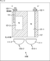
- FIG. 9 a high sensitivity photodiode (PD) 121-1 and a low sensitivity photodiode (PD) 121-2 are formed in silicon (Si) of a semiconductor substrate 112.
- the size of the high sensitivity photodiode 121-1 and the low sensitivity photodiode 121-2 in the planar direction is equal (substantially the same) or larger.
- the size of the low sensitivity photodiode 121-2 in the depth direction is smaller than the size of the high sensitivity photodiode 121-1 in the depth direction.
- the vertical transistor 131 is formed on the silicon (Si) of the semiconductor substrate 112, and the charge accumulated in the low-sensitivity photodiode 121-2 is transferred to the third transfer transistor 122- through the vertical transistor 131. 3 is read.
- the size of the low sensitivity photodiode 121-2 is limited, and the high sensitivity photodiode is limited.
- the size in the depth direction is smaller than that of 121-1.
- the sensitivity of the low-sensitivity pixel 101B-2 can be adjusted by changing the position of the low-sensitivity photodiode 121-2 in the depth direction.
- the sensitivity of the low-sensitivity pixel 101B-2 improves as the position in the depth direction of the low-sensitivity photodiode 121-2 moves toward the light incident side, while the sensitivity of the low-sensitivity pixel 101B-2 increases toward the wiring side.
- the sensitivity difference between the high-sensitivity pixel 101B-1 and the low-sensitivity pixel 101B-2 is optimized by setting the position of the low-sensitivity photodiode 121-2 in the depth direction to an appropriate position. be able to.
- the planar direction of the high sensitivity photodiode 121-1 and the low sensitivity photodiode 121-2. are equal (substantially the same size).
- the low sensitivity photodiode 121-2 in the depth direction has been described, but the size (width) of the low-sensitivity photodiode 121-2 in the planar direction is changed. Also good.
- the low sensitivity photodiode can be obtained by forming the vertical transistor 131 according to the structure. The charge accumulated in 121-2 can be read out.
- the pixel 100B has the cross-sectional structure shown in FIG. 8 and FIG. 9, so that the low-sensitivity pixel 101B-2 reduces the amount of charge generated as a result of photoelectric conversion and generates the generated charge. The amount that can be stored is increased. Thereby, the pixel 100B can obtain characteristics with a wide dynamic range.
- both the high-sensitivity pixel 101B-1 and the low-sensitivity pixel 101B-2 accumulate the generated charges in the photodiode, so that the S / N is good in both the low and high illuminance regions. Characteristics can be obtained.
- the sensitivity of the low-sensitivity pixel 101B-2 can be adjusted by changing the position in the depth direction of the low-sensitivity photodiode 121-2 and the size (width) in the planar direction.
- the pixel 100C having a structure in which the low-sensitivity pixel has a pixel internal capacitance (FC) will be described.
- FIG. 10 is a plan view showing the structure of the pixel 100C.
- a in FIG. 10 represents a plan view when one of the pixels 100C arranged two-dimensionally in the pixel array unit 11 of the CMOS image sensor 10 (FIG. 1) is viewed from the wiring side.
- B in FIG. 10 represents a plan view when the pixel 100C is viewed from the light incident side.
- FIG. 11 a high-sensitivity photodiode (PD) 121-1 and a low-sensitivity photodiode (PD) 121-2 are formed in silicon (Si) of a semiconductor substrate 112.
- the size (area of the light receiving surface) in the planar direction of the high sensitivity photodiode 121-1 and the low sensitivity photodiode 121-2 is the same (approximately).
- the size in the depth direction of the low-sensitivity photodiode 121-2 is smaller than the size in the depth direction of the high-sensitivity photodiode 121-1.
- the low-sensitivity pixel 101C-2 has a pixel internal capacitance (FC) 123 as shown in the plan view on the wiring side of FIG. This is different from the structure of the low-sensitivity pixel 101A-2 of the pixel 100A shown in the plan view on the wiring side. That is, in the low-sensitivity pixel 101C-2, the charges overflowing from the low-sensitivity photodiode 121-2 are accumulated by the pixel capacitance 123.
- FC pixel internal capacitance
- the saturation charge amount (Qs) of the low sensitivity pixel 101C-2 overflows to the in-pixel capacitance 123. It will be expanded according to the amount of charge.
- the size of the low-sensitivity photodiode 121-2 in the planar direction can be equal to or larger than the size of the high-sensitivity photodiode 121-1 in the planar direction. Saturation charge (Qs) can be gained to some extent, so it is superior in S / N characteristics at low illumination.
- the pixel 100C has the cross-sectional structure shown in FIGS. 10 and 11, and thus contributes to the saturation charge amount (Qs) of the low-sensitivity pixel 101C-2. Since a certain amount of saturation charge (Qs) can be obtained without reducing the size in the plane direction, it is difficult for the charge to overflow into the pixel internal capacity 123, which is superior in S / N characteristics at low illumination. .
- the saturation charge amount (Qs) of the low sensitivity pixel 101C-2 is the charge overflowed to the in-pixel capacitance 123. It will be expanded according to the amount.
- the low-sensitivity pixel has a pixel internal capacitance (FC), and the position of the low-sensitivity photodiode (PD) in the depth direction is changed.
- FC pixel internal capacitance
- PD low-sensitivity photodiode
- FIG. 12 is a plan view showing the structure of the pixel 100D.
- a in FIG. 12 represents a plan view when one of the pixels 100D arranged two-dimensionally in the pixel array unit 11 of the CMOS image sensor 10 (FIG. 1) is viewed from the wiring side.
- B of FIG. 12 represents a plan view when the pixel 100D is viewed from the light incident side.
- FIG. 13 a high sensitivity photodiode (PD) 121-1 and a low sensitivity photodiode (PD) 121-2 are formed in silicon (Si) of a semiconductor substrate 112.
- the size (area of the light receiving surface) in the planar direction of the high sensitivity photodiode 121-1 and the low sensitivity photodiode 121-2 is the same (substantially).
- the size in the depth direction of the low-sensitivity photodiode 121-2 is smaller than the size in the depth direction of the high-sensitivity photodiode 121-1.
- the position of the low sensitivity photodiode 121-2 in the depth direction is changed from the position on the wiring side to the position closer to the light incident side.
- the sensitivity of the low sensitivity pixel 101D-2 is adjusted.
- the charge accumulated in the low-sensitivity photodiode 121-2 is read out by the third transfer transistor 122-3 via the vertical transistor 131.
- the low-sensitivity pixel 101D-2 has a pixel internal capacitance (FC) 123. This is different from the structure of the low-sensitivity pixel 101B-2 of the pixel 100B shown in the plan view on the wiring side. That is, in the low-sensitivity pixel 101D-2, the charges overflowing from the low-sensitivity photodiode 121-2 are accumulated by the pixel capacitance 123.
- FC pixel internal capacitance
- the saturation charge amount (Qs) of the low sensitivity pixel 101D-2 overflows to the in-pixel capacitance 123. It will be expanded according to the amount of charge.
- the low-sensitivity photodiode 121-2 of the low-sensitivity pixel 101D-2 is formed at a position away from the ion-implanted wiring side, so that it is difficult to form a steep PN junction.
- the saturation charge amount (Qs) of only the low sensitivity photodiode 121-2 becomes small.
- the charge from the low-sensitivity photodiode 121-2 overflows and accumulates in the pixel capacitance 123, so there is no problem with the saturation charge amount (Qs) as the low-sensitivity pixel 101D-2.
- the pixel 100D has the cross-sectional structure shown in FIGS. 12 and 13, and thus contributes to the saturation charge amount (Qs) of the low-sensitivity pixel 101D-2.
- a certain amount of saturation charge (Qs) can be earned without reducing the size in the planar direction.
- the saturation charge amount (Qs) of the low sensitivity pixel 101D-2 is the charge overflowed to the in-pixel capacitance 123. It will be expanded according to the amount.
- the sensitivity of the low-sensitivity pixel 101D-2 can be adjusted by changing the position in the depth direction and the size (width) in the planar direction of the low-sensitivity photodiode 121-2.
- the pixels 100A to 100D have been described as the second embodiment.
- the sensitivity is lowered, and the size of the low-sensitivity pixel in the planar direction of the low-sensitivity photodiode is reduced. Is equal to or larger than the size of the high-sensitivity photodiode in the planar direction.
- the amount of generated charges can be accumulated while reducing the amount of charges generated as a result of photoelectric conversion.
- the pixels 100A to 100D can obtain characteristics with a wide dynamic range.
- a certain amount of saturation charge (Qs) can be obtained, so that it is difficult for the charge to overflow into the pixel internal capacity, and the S / N has a characteristic advantage.
- the “depth direction” of silicon (Si) of the semiconductor substrate 112 described above is an “optical axis direction” in which light enters.
- the “plane direction” is a “direction perpendicular to the optical axis”.
- FC Floating Capacitor
- LFIC Lateral Over Flow Integration Capacitor
- the photodiode is formed by implanting ions from the wiring side. This makes it easier to form a high-capacity photodiode using a PN junction. That is, in order to increase the saturation charge amount (Qs) of the low-sensitivity pixel, the size in the plane direction on the wiring side of the low-sensitivity photodiode may be increased. The higher the saturation charge amount (Qs) of the low-sensitivity photodiode of the low-sensitivity pixel, the higher the dynamic range can be obtained.
- the size of the low-sensitivity pixel in the plane direction on the wiring side of the low-sensitivity photodiode is made larger than the size in the plane direction on the light incident side so that the saturation charge amount ( Qs) can be expanded.
- the saturation charge amount (Qs) of the low-sensitivity pixel is increased, and a high dynamic range can be obtained.
- the pixels 200A to 200F are described as the pixels 200 arranged two-dimensionally in the pixel array unit 11 of the CMOS image sensor 10 (FIG. 1). However, the pixels 200A and 200F are described.
- the pixel 200B to the pixel 200E have a structure having the pixel capacitor 223, while the pixel 200B to the pixel 200E have a structure without the pixel capacitor 223.
- pixel circuits such as the high-sensitivity photodiode 221-1, the low-sensitivity photodiode 221-2, and the first transfer transistor 222-1 to the selection transistor 229 have high sensitivity in the pixel 100 in FIG. This corresponds to pixel circuits such as the photodiode 121-1, the low-sensitivity photodiode 121-2, and the first transfer transistor 122-1 to the selection transistor 129.
- the pixel circuits of the pixel 200B and the pixel 200E correspond to the configuration of the pixel circuit shown in FIG. 2, but the pixel circuits of the pixel 200A and the pixel 200F have a pixel internal capacitance 223 in the pixel circuit shown in FIG. This corresponds to a configuration in which no is provided.
- (2-A) Basic structure Structure in which the incident light side and the wiring side of the low sensitivity PD have different sizes in the plane direction
- a pixel 200A having a structure in which the size of the incident light side and the wiring side of the low sensitivity photodiode (PD) are different from each other will be described.
- FIG. 14 is a plan view showing the structure of the pixel 200A.
- a in FIG. 14 represents a plan view when one of the pixels 200A arranged two-dimensionally in the pixel array section 11 of the CMOS image sensor 10 (FIG. 1) is viewed from the wiring side.
- B of FIG. 14 represents a plan view when the pixel 200A is viewed from the light incident side.
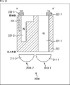
- FIG. 15 a high sensitivity photodiode (PD) 221-1 and a low sensitivity photodiode (PD) 221-2 are formed in silicon (Si) of a semiconductor substrate 212.
- the high-sensitivity photodiode 221-1 generates and accumulates charges corresponding to the amount of light incident through the on-chip lens 211-1.
- the charge accumulated by the high sensitivity photodiode 221-1 is read out by a pixel circuit such as the first transfer transistor 222-1.
- a high-sensitivity pixel 201A-1 is configured by a pixel circuit such as the above.
- the low-sensitivity photodiode 221-2 generates and accumulates charges corresponding to the amount of light incident through the on-chip lens 211-2. Then, the charge accumulated by the high sensitivity photodiode 221-2 is read out by the pixel circuit such as the third transfer transistor 222-3 via the vertical transistor 231.
- a low-sensitivity pixel 201A-2 is configured by a pixel circuit such as the above.
- the size of the low-sensitivity photodiode 221-2 in the depth direction is the size of the high-sensitivity photodiode 221-1 in the depth direction. It becomes a smaller size.
- the size of the low-sensitivity photodiode 221-2 in the planar direction is different from the size in the planar direction on the light incident side and the size in the planar direction on the wiring side. Specifically, in the low sensitivity photodiode 221-2, the size in the plane direction on the wiring side is larger than the size in the plane direction on the light incident side.
- the difference in sensitivity between the high-sensitivity pixel 201A-1 and the low-sensitivity pixel 201A-2 is set by the size of the photodiode in the depth direction, and thus the planar direction of the low-sensitivity photodiode 221-2. Is not required to be smaller than the size of the high-sensitivity photodiode 221-1 in the planar direction, and can be equal to or larger than the size of the high-sensitivity photodiode 221-1.
- the size of the light incident side plane direction contributing to the sensitivity of the low sensitivity photodiode 221-2 of the low sensitivity pixel 201A-2 is set to the plane on the wiring side contributing to the saturation charge amount (Qs).
- the high sensitivity photodiode 221-1 of the high sensitivity pixel 201A-1 and the low sensitivity photodiode 221-2 of the low sensitivity pixel 201A-2 are formed on the semiconductor substrate 212, ions are implanted from the wiring side. As a result, a photodiode is formed. On the wiring side, it becomes easier to form a high-capacity photodiode by a PN junction.
- the size of the low-sensitivity photodiode 221-2 on the wiring side may be increased, and the low-sensitivity photodiode 221-2. Then, the size in the plane direction on the wiring side is set to be larger than the size in the plane direction on the light incident side. Thereby, the saturation charge amount (Qs) of the low-sensitivity pixel 201A-2 is increased, and a high dynamic range can be obtained.
- the pixel 200A has the structure shown in FIGS. 14 and 15, and thereby contributes to the saturation charge amount (Qs) of the low-sensitivity pixel 101A-2.
- the saturation charge amount (Qs) of the low-sensitivity pixel 201A-2 can be increased by widening the size in the planar direction of the light incident side.
- the plane size on the light incident side of the low sensitivity photodiode 221-2 that contributes to the sensitivity of the low sensitivity pixel 201A-2 is smaller than the size in the plane direction on the wiring side. While the saturation charge amount (Qs) of the high-sensitivity pixel 201A-1 and the low-sensitivity pixel 201A-2 is ensured to be equal to or higher, the sensitivity of the low-sensitivity pixel 201A-2 can be further reduced. The effect of expanding the dynamic range in the pixel 200A is increased.
- a pixel 200B having a structure in which a low-sensitivity pixel has a pixel internal capacitance (FC) will be described with reference to a plan view of FIG. 16 and a cross-sectional view of FIG.
- FIG. 16 is a plan view showing the structure of the pixel 200B.
- a in FIG. 16 represents a plan view when one of the pixels 200B arranged two-dimensionally in the pixel array unit 11 of the CMOS image sensor 10 (FIG. 1) is viewed from the wiring side.
- B of FIG. 16 represents a plan view when the pixel 200B is viewed from the light incident side.
- FIG. 17 a high sensitivity photodiode (PD) 221-1 and a low sensitivity photodiode (PD) 221-2 are formed in silicon (Si) of the semiconductor substrate 112.
- the size of the low sensitivity photodiode 221-2 in the depth direction is larger than the size of the high sensitivity photodiode 221-1 in the depth direction. Small size.
- the size in the plane direction on the wiring side is larger than the size in the plane direction on the light incident side.
- the low sensitivity pixel 201B-2 has a pixel internal capacity (FC) 223. This is different from the structure of the low-sensitivity pixel 201A-2 of the pixel 200A shown in the plan view of FIG. That is, in the low-sensitivity pixel 201B-2 of the pixel 200B, the charges overflowing from the low-sensitivity photodiode 221-2 are accumulated by the pixel capacitance 223.
- FC pixel internal capacity
- the pixel 200B has the structure shown in FIGS. 16 and 17, and thereby contributes to the saturation charge amount (Qs) of the low-sensitivity pixel 101B-2, which is on the wiring side of the low-sensitivity photodiode 221-2.
- the saturation charge amount (Qs) of the low-sensitivity pixel 201B-2 can be increased by expanding the size in the planar direction of the light-receiving side.
- the plane size on the light incident side of the low sensitivity photodiode 221-2 that contributes to the sensitivity of the low sensitivity pixel 201B-2 is smaller than the size in the plane direction on the wiring side. While the saturation charge amount (Qs) of the high-sensitivity pixel 201B-1 and the low-sensitivity pixel 201B-2 is ensured to be equal to or higher, the sensitivity of the low-sensitivity pixel 201B-2 can be further reduced. The effect of expanding the dynamic range in the pixel 200B is increased.
- the saturation charge amount (Qs) of the low-sensitivity pixel 201B-2 is the charge overflowed to the in-pixel capacitance 223. It will be expanded according to the amount.
- a pixel 200C having a structure in which a low-sensitivity photodiode (PD) is formed around the high-sensitivity photodiode (PD) will be described with reference to a plan view of FIG. 18 and a cross-sectional view of FIG.
- FIG. 18 is a plan view showing the structure of the pixel 200C.
- a in FIG. 18 represents a plan view when one of the pixels 200 ⁇ / b> C arranged two-dimensionally in the pixel array unit 11 of the CMOS image sensor 10 (FIG. 1) is viewed from the wiring side.
- B of FIG. 18 represents a plan view when the pixel 200C is viewed from the light incident side.
- FIG. 19 a high-sensitivity photodiode (PD) 221-1 and a low-sensitivity photodiode (PD) 221-2 are formed in the silicon (Si) of the semiconductor substrate 212.
- Reference numeral 221-2 is formed around (around) the high-sensitivity photodiode 221-1 (a plan view on the light incident side in FIG. 18).
- the low-sensitivity photodiode 221-2 of the low-sensitivity pixel 201C-2 is formed in a region outside the condensing point of the on-chip lens 211, so that the high-sensitivity pixel 201C-1 And a low sensitivity pixel 201C-2.
- the size of the high-sensitivity photodiode 221-1 in the planar direction is different between the light incident side and the wiring side. Specifically, in the high sensitivity photodiode 221-1, the size in the planar direction on the wiring side is smaller than the size in the planar direction on the light incident side.
- the size of the low-sensitivity photodiode 221-2 in the planar direction is different between the light incident side and the wiring side. Specifically, in the low-sensitivity photodiode 221-2, the size in the plane direction on the wiring side is larger than the size in the plane direction on the light incident side.
- the saturation charge amount (Qs) of the low-sensitivity photodiode 221-2 of the low-sensitivity pixel 201C-2 is larger, a higher dynamic range can be expected. Therefore, also in the pixel 200C, the above-described pixel 200A (FIG. 15). Similarly to the pixel 200B (FIG. 17), the size of the low sensitivity photodiode 121-2 in the plane direction on the wiring side is made larger than the size in the plane direction on the light incident side.
- the size in the planar direction on the wiring side of the high-sensitivity photodiode 221-1 is set in order to secure a region for increasing the size in the planar direction on the wiring side of the low-sensitivity photodiode 121-2. It is small.
- the pixel 200C has a structure in which the low sensitivity pixel 201C-2 is arranged around (periphery) the high sensitivity pixel 201C-1, so that the low sensitivity photodiode 221 of the low sensitivity pixel 201C-2 is provided. -2 is formed in a region deviated from the condensing point of the on-chip lens 211, and thus the sensitivity can be reduced.
- the saturation charge amount (Qs) is ensured by setting the size in the plane direction on the wiring side to be larger than the size in the plane direction on the light incident side in the low-sensitivity photodiode 221-2.
- the sensitivity can be lowered.
- a part of the low-sensitivity photodiode 221-2 has a high-sensitivity photodiode. Although it is smaller than the diode 221-1, the entire low sensitivity photodiode 221-2 may be smaller than the high sensitivity photodiode 221-1.
- the pixel 200C has the structure shown in FIGS. 18 and 19, and thereby contributes to the saturation charge amount (Qs) of the low-sensitivity pixel 101C-2.
- the saturation charge amount (Qs) of the low-sensitivity pixel 201C-2 can be increased by widening the size in the planar direction of the pixel.
- the plane size on the light incident side of the low sensitivity photodiode 221-2 that contributes to the sensitivity of the low sensitivity pixel 201C-2 is smaller than the size in the plane direction on the wiring side.
- the saturation charge amount (Qs) of the high-sensitivity pixel 201C-1 and the low-sensitivity pixel 201C-2 can be equalized or higher, and the sensitivity of the low-sensitivity pixel 201C-2 can be further reduced. The effect of expanding the dynamic range in the pixel 200C is increased.
- a pixel 200D having a structure in which the wiring side of a high-sensitivity photodiode (PD) is formed by a PN junction will be described with reference to the plan view of FIG. 20 and the cross-sectional views of FIGS.
- FIG. 20 is a plan view showing the structure of the pixel 200D.
- a in FIG. 20 represents a plan view when one of the pixels 200D arranged two-dimensionally in the pixel array section 11 of the CMOS image sensor 10 (FIG. 1) is viewed from the wiring side.
- B of FIG. 20 represents a plan view when the pixel 200D is viewed from the light incident side.
- the structure shown in the cross sectional view of FIG. 21 is obtained.
- the pixel 200D of FIG. 21 as in the pixel 200C (FIG. 19) described above, the low sensitivity photodiode 221-2 is formed around (around) the high sensitivity photodiode 221-1 (B in FIG. 20). Plan view of the light incident side of FIG.
- the low-sensitivity photodiode 221-2 of the low-sensitivity pixel 201D-2 is formed in a region outside the condensing point of the on-chip lens 211, so that the high-sensitivity pixel 201D- 1 and a low sensitivity pixel 201D-2.
- the pixel 200D has a size in the plane direction on the wiring side smaller than the size in the plane direction on the light incident side in the high-sensitivity photodiode 221-1.
- the size in the plane direction on the wiring side is larger than the size in the plane direction on the light incident side.
- an N + layer 213 that is an N-type region and a P + layer 214 that is a P-type region are formed on the wiring side of the high-sensitivity photodiode 221-1, and a PN junction is formed.
- ions are implanted into the semiconductor substrate 212 from the wiring side. It is easy to form a high-capacity photodiode. That is, in order to increase the saturation charge amount (Qs), the size in the planar direction on the wiring side of the photodiode may be increased.
- the wiring of the low-sensitivity photodiode 121-2 The size in the plane direction on the side is increased.
- the size in the planar direction on the wiring side of the high-sensitivity photodiode 221-1 is reduced.
- both the high-sensitivity photodiode 221-1 of the high-sensitivity pixel 201D-1 and the low-sensitivity photodiode 221-2 of the low-sensitivity pixel 201D-2 are connected to the plane direction on the light incident side and the wiring side.
- the size is different in the plane direction.
- a PN junction that contributes to the saturation charge amount (Qs) is formed on the wiring side, so that the high-capacity high-sensitivity photodiode 221- 1 is formed. 1 is formed.
- a PN junction may also be formed at a portion in the middle of reducing the size of the high-sensitivity photodiode 221-1 in the planar direction.
- a PN junction is formed in the pixel 200E.
- the pixel 200D has the structure shown in FIGS. 20 and 21, and the pixel 200E has the structure shown in FIGS. 20 and 22. Therefore, the low-sensitivity pixel 201D-2 (201E-2 ) That contributes to the saturation charge amount (Qs) of the low-sensitivity photodiode 221-2, the size in the plane direction on the wiring side of the low-sensitivity photodiode 221-2 is made wider than the size in the plane direction on the light incident side, thereby reducing the low-sensitivity pixel 201D-2 (201E Since the saturation charge amount (Qs) of -2) can be increased, a high dynamic range can be obtained.
- the saturation charge amount (Qs) of -2 Since the saturation charge amount (Qs) of -2) can be increased, a high dynamic range can be obtained.
- the plane size on the light incident side of the low sensitivity photodiode 221-2 that contributes to the sensitivity of the low sensitivity pixel 201D-2 (201E-2) is smaller than the size in the plane direction on the wiring side. Therefore, the saturation charge amount (Qs) of the high-sensitivity pixel 201D-1 (201E-1) and the low-sensitivity pixel 201D-2 (201E-2) is ensured to be equal to or higher than the low-sensitivity pixel 201D-2.
- the sensitivity of (201E-2) can be further reduced, and the effect of expanding the dynamic range in the pixel 200D is increased.
- the pixel 200F will be described with reference to the cross-sectional view of FIG.
- the size in the depth direction of the low sensitivity photodiode 221-2 is larger than the size in the depth direction of the high sensitivity photodiode 221-1 in the same manner as the pixel 200A (FIG. 15) described above. Small size.
- the size in the plane direction on the wiring side is larger than the size in the plane direction on the light incident side.
- the external size of the on-chip lens 211-2 that condenses the light on the low-sensitivity photodiode 221-2 is in the plane direction on the light incident side of the low-sensitivity photodiode 221-2. It is matched to the size.
- the on-chip lens 211-1 of the high-sensitivity pixel 201A-1 and the on-chip lens 211-2 of the low-sensitivity pixel 201A-2 have the same outer size.
- the on-chip lens 211-1 of the high-sensitivity pixel 201F-1 and the on-chip lens 211-2 of the low-sensitivity pixel 201F-2 are different from each other in the pixel 200F in FIG.
- the external size of the on-chip lens 211-2 can be changed according to the size of the low-sensitivity photodiode 221-2 in the planar direction on the light incident side.
- the pixels 200A to 200F have been described as the third embodiment.
- the size of the low-sensitivity pixel in the planar direction on the wiring side of the low-sensitivity photodiode is made larger than the size in the planar direction on the light incident side, and the saturation charge amount ( Qs) can be extended.
- the saturation charge amount (Qs) of the high-sensitivity pixel and the low-sensitivity pixel can be equalized or higher, and the sensitivity of the low-sensitivity pixel can be further reduced. This is advantageous for expanding the dynamic range of pixels having the.
- the sensitivity difference between the high-sensitivity pixel and the low-sensitivity pixel is limited by limiting the size of the low-sensitivity photodiode in the depth direction.
- limiting the size it is possible to adopt a structure in which a pixel internal capacitance (FC) or the like is stacked on a low-sensitivity photodiode.
- the size of the low-sensitivity photodiode in the depth direction is limited, and the low-sensitivity photodiode has a structure in which a pixel internal capacitance (FC) is stacked.
- FC pixel internal capacitance
- the pixels 300A to 300E are described as the pixels 300 arranged two-dimensionally in the pixel array unit 11 of the CMOS image sensor 10 (FIG. 1).
- pixel circuits such as the high-sensitivity photodiode 321-1, the low-sensitivity photodiode 321-2, and the first transfer transistor 322-1 to the selection transistor 329 have high sensitivity in the pixel 100 in FIG. This corresponds to pixel circuits such as the photodiode 121-1, the low-sensitivity photodiode 121-2, and the first transfer transistor 122-1 to the selection transistor 129.
- the pixel circuit of the pixel having the intra-pixel capacitance 323 corresponds to the configuration of the pixel circuit shown in FIG. 2, and the pixel circuit of the pixel not having the intra-pixel capacitance 323 is shown in FIG. This corresponds to the configuration in which the pixel capacitor 323 is not provided in the pixel circuit shown in FIG.
- a pixel 300A having a structure in which a low sensitivity photodiode (PD) and a pixel capacitance (FC) are stacked will be described with reference to FIGS.
- PD low sensitivity photodiode
- FC pixel capacitance
- FIG. 24 is a plan view showing the structure of the pixel 300A.
- FIG. 24 is a plan view when one of the pixels 300 ⁇ / b> A arranged two-dimensionally in the pixel array unit 11 of the CMOS image sensor 10 (FIG. 1) is viewed from the wiring side.
- FIG. 25 a high sensitivity photodiode (PD) 321-1 and a low sensitivity photodiode (PD) 321-2 are formed in silicon (Si) of a semiconductor substrate 312.
- the size of the high-sensitivity photodiode 321-1 and the low-sensitivity photodiode 321-2 in the planar direction is the same as that of the pixel 100 of the second embodiment (for example, the pixel 100A of FIG. 7). (Area of the light receiving surface) is the same size, but the size of the low sensitivity photodiode 321-2 in the depth direction is smaller than the size of the high sensitivity photodiode 321-1 in the depth direction. .
- the position of the low-sensitivity photodiode 321-2 in the depth direction is not on the wiring side but on the light incident side, so that the silicon (Si) of the semiconductor substrate 312 has a vertical position.
- a type transistor 331 is formed. The charges accumulated in the low sensitivity photodiode 321-2 are read out by the vertical transistor 331.
- the pixel 300A silicon (Si) of the semiconductor substrate 312 is dug from the wiring side, and a trench type pixel internal capacitor (FC) 323A is buried in the dug portion. That is, in the pixel 300A, the low-sensitivity photodiode 321-2 and the pixel internal capacitance 323A have a laminated structure.
- the size of the high sensitivity photodiode 321-1 in the planar direction is set.
- Can be extended (PDL extension area" in FIG. 24).
- the difference in size in the plane direction between the high sensitivity photodiode 321-1 and the low sensitivity photodiode 321-2 can be further increased, and thus the high sensitivity pixel 301A-1 and the low sensitivity pixel 301A.
- the sensitivity difference from -2 can be further increased.
- FIG. 26 shows an example of the structure of the trench type pixel internal capacitance 323A of FIG. 26, an N ⁇ layer 353 corresponding to the lower electrode is formed on the inner wall and the bottom surface of the digging portion 350 dug from the wiring side. Further, a capacitor film 352 is formed on the inner wall surface and bottom surface in the digging portion 350 and on the substrate in the formation region of the pixel capacitor 323A.
- An upper electrode 351 is formed on the capacitor film 352 so as to fill the digging portion 350 and protrude from the substrate surface.
- an element isolation portion 354 is formed around the pixel capacitor 323A.
- an N + layer 355 corresponding to the source of the transfer transistor is formed on the surface of the substrate located on the right side of the pixel internal capacitor 323A.
- the pixel 300A has the structure shown in FIGS. 24 to 26, so that the high-sensitivity photo expanded to the PDL extension region (the region secured by forming the pixel capacitor 323A in a stacked structure).
- the sensitivity of the diode 321-1 can be further increased than the sensitivity of the low sensitivity photodiode 321-2.
- the sensitivity difference between the high sensitivity pixel 301A-1 and the low sensitivity pixel 301A-2 can be further expanded.
- a pixel 300B having a structure in which a low-sensitivity photodiode (PD) and an oxide film are stacked will be described with reference to a cross-sectional view of FIG.
- the cross-sectional view of FIG. 27 corresponds to the cross-section of the dotted line XX ′ in the plan view of FIG.
- the size of the low sensitivity photodiode 321-2 in the depth direction is smaller than the size of the high sensitivity photodiode 321-1 in the depth direction, as in the pixel 300A of FIG. Become.
- the charge accumulated in the low sensitivity photodiode 321-2 is read out by the vertical transistor 331.
- an oxide film 341 is embedded in a dug portion from the wiring side formed in silicon (Si) of the semiconductor substrate 312. That is, as in the pixel 300A (FIG. 25), when the in-pixel capacitor 323A is not stacked with the low sensitivity photodiode 321-2, a structure in which the oxide film 341 is embedded in the digging portion can be employed. Thereby, in the pixel 300B, the low-sensitivity photodiode 321-2 and the oxide film 341 have a laminated structure.
- the material embedded in the digging portion formed in the semiconductor substrate 312 is not limited to the oxide film 341, and other materials may be embedded.
- (3-C) A structure in which a low-sensitivity PD and an oxide film are stacked (digging from the light incident side)
- a pixel 300C having a structure in which a low-sensitivity photodiode (PD) and an oxide film are stacked will be described with reference to a cross-sectional view of FIG.
- the cross-sectional view of FIG. 28 corresponds to the cross section of the dotted line XX ′ in the plan view of FIG.
- the size of the low sensitivity photodiode 321-2 in the depth direction is smaller than the size of the high sensitivity photodiode 321-1 in the depth direction, similar to the pixel 300B of FIG. Become.
- the position of the low-sensitivity photodiode 321-2 in the depth direction is not on the light incident side but on the wiring side, so that the third transfer transistor 322-3 is directly low
- the charge accumulated in the sensitivity photodiode 321-2 is read out.
- the vertical transistor 331 is different from the structure of the pixel 300B (FIG. 27) in which charges are read from the low-sensitivity photodiode 321-2.
- silicon (Si) of the semiconductor substrate 312 is dug from the light incident side, and an oxide film 341 is buried in the dug portion. That is, as in the pixel 300A (FIG. 25), when the in-pixel capacitor 323A is not stacked with the low-sensitivity photodiode 321-2, a structure in which the oxide film 341 is embedded in the digging portion can be employed.
- the oxide film 341 can be embedded in a dug portion dug from the wiring side or the light incident side. Thereby, in the pixel 300C, the low sensitivity photodiode 321-2 and the oxide film 341 have a laminated structure.
- the material embedded in the digging portion formed in the semiconductor substrate 312 is not limited to the oxide film 341, and other materials may be embedded.
- FIG. 29 corresponds to the cross section of the dotted line XX ′ in the plan view of FIG.
- the size in the depth direction of the low sensitivity photodiode 321-2 is smaller than the size in the depth direction of the high sensitivity photodiode 321-1 in the same manner as the pixel 300A in FIG. Become.
- the charge accumulated in the low sensitivity photodiode 321-2 is read out by the vertical transistor 331.
- a trench-type pixel internal capacitor 323A is embedded in the digging portion from the silicon (Si) wiring side of the semiconductor substrate 312 and the low-sensitivity photodiode 321- 2 and the pixel internal capacity 323A have a laminated structure.
- the region of the pixel internal capacitance 323 (323A) stacked on the low sensitivity photodiode 321-2 is allocated to the region of the high sensitivity photodiode 321-1.
- the size in the planar direction of the high-sensitivity photodiode 321-1 can be expanded.
- the region of the high-sensitivity photodiode 321-1 can be expanded to the PDL expansion region (FIG. 24).
- the sensitivity difference between the pixel 301A-1 and the low sensitivity pixel 301A-2 can be further enlarged.
- the pixel 300D employs an RDTI structure between the high-sensitivity photodiode 321-1 and the low-sensitivity photodiode 321-2, color mixing can be suppressed.
- the pixel 300D is equivalent to the structure in which the light shielding film 343 is provided for the pixel 300A (FIG. 25), but similarly to the pixel 300B (FIG. 27) or the pixel 300C (FIG. 28). You may make it employ
- FIGS. 30 and 31 a pixel 300E having a structure in which a low-sensitivity photodiode (PD) and a pixel internal capacitance (FC) are stacked will be described.
- the cross-sectional view of FIG. 30 corresponds to the cross section of the dotted line XX ′ in the plan view of FIG.
- the size of the low sensitivity photodiode 321-2 in the depth direction is smaller than the size of the high sensitivity photodiode 321-1 in the depth direction, as in the pixel 300A of FIG. Become.
- the charge accumulated in the low sensitivity photodiode 321-2 is read by the vertical transistor 331.
- a trench-type pixel internal capacitor 323B is embedded in a digging portion from the silicon (Si) wiring side of the semiconductor substrate 312 and a low-sensitivity photodiode 321- 2 and the in-pixel capacitor 323B have a laminated structure.
- FIG. 31 shows an example of the structure of the trench type intra-pixel capacitor 323B of FIG.
- a P-layer 363 is formed as a lower electrode on the inner wall surface and the bottom surface of the first digging portion 360a.
- This P ⁇ layer 363 is connected to the P well layer of the substrate.
- a capacitive film 362 is formed on the inner wall surface and the bottom surface of the first digging portion 360a.
- a trench-type upper electrode 361 is formed on the substrate so as to cover the capacitance film 362 and bury the second digging portion 360b formed in the vicinity of the substrate surface.
- the intra-pixel capacitor 323B is configured by connecting an N + layer 365 corresponding to the source of the transfer transistor and an upper electrode 361.
- the pixel 300E has the same structure as the pixel 300A (FIG. 25) except that an in-pixel capacitor 323B is embedded instead of the in-pixel capacitor 323A. Therefore, also in the pixel 300E, by assigning the region of the in-pixel capacitance 323B stacked on the low sensitivity photodiode 321-2 to the region of the high sensitivity photodiode 321-1, the planar direction of the high sensitivity photodiode 321-1 The size of can be expanded.
- the region of the high-sensitivity photodiode 321-1 can be expanded to the PDL expansion region (FIG. 24). Therefore, the sensitivity difference between the high sensitivity pixel 301A-1 and the low sensitivity pixel 301A-2 is further enlarged.
- the pixels 300A to 300E have been described as the fourth embodiment.
- the size of the low-sensitivity photodiode in the depth direction is limited, and the low-sensitivity photodiode has a structure in which a pixel capacitance (FC) is stacked.
- the obtained space (for example, the PDL expansion region in FIG. 24) can be used to expand the size of the high sensitivity photodiode in the planar direction. As a result, the sensitivity difference between the high sensitivity pixel and the low sensitivity pixel can be further expanded.
- the size of the low-sensitivity pixel in the depth direction of the low-sensitivity photodiode is limited. Since the size of the sensitivity photodiode in the planar direction (area of the light receiving surface) can be increased, and a pixel internal capacitance (charge storage unit) can be provided for the low sensitivity photodiode, characteristics with a wide dynamic range can be obtained. be able to.
- FIG. 32 Next, a fifth embodiment will be described with reference to FIGS. 32 to 36.
- FIG. 32 Next, a fifth embodiment will be described with reference to FIGS. 32 to 36.
- a so-called moth-eye structure in which a minute uneven structure is provided at the interface on the light-receiving surface side (light incident side) of a silicon layer in which a photodiode is formed in a pixel.
- this moth-eye structure it is possible to prevent reflection of incident light, but since incident light can be diffracted, it is possible to increase the optical path length of light that is subject to photoelectric conversion in the photodiode. it can.
- the sensitivity of the photodiode can be increased if the optical path length of the light to be subjected to photoelectric conversion can be increased.
- this principle is utilized.
- a highly sensitive pixel with higher sensitivity can be formed.
- this principle is used to expand the dynamic range of pixels having high sensitivity pixels and low sensitivity pixels.
- the pixels 400A to 400D are described as the pixels 400 arranged two-dimensionally in the pixel array unit 11 of the CMOS image sensor 10 (FIG. 1).
- pixel circuits such as the high-sensitivity photodiode 421-1, the low-sensitivity photodiode 421-2, and the first transfer transistor 422-1 to the selection transistor 429 have high sensitivity in the pixel 100 in FIG. This corresponds to pixel circuits such as the photodiode 121-1, the low-sensitivity photodiode 121-2, and the first transfer transistor 122-1 to the selection transistor 129.
- a pixel 400A in which a high-sensitivity photodiode (PD) has a moth-eye structure will be described with reference to a cross-sectional view of FIG.
- FIG. 32 as an example of the pixel 400A arranged two-dimensionally in the pixel array section 11 of the CMOS image sensor 10 (FIG. 1), a pixel composed of a high sensitivity pixel 401A-1 and a low sensitivity pixel 401A-2 is shown. It is shown in the figure.
- an N-type photodiode 421 is formed for each pixel on P-type silicon (Si).
- the size in the planar direction (area of the light receiving surface) of each photodiode 421 formed in the semiconductor substrate 412 and the size in the depth direction of silicon (Si) are the same size.
- the external size of the on-chip lens 411 on which light is incident on each photodiode 421 is also the same size.
- the moth-eye structure is formed at the interface (light-receiving surface side interface) of the P-type semiconductor region above the photodiode 421-1.
- a fine concavo-convex structure is formed.
- the moth-eye structure is not formed above the photodiode 421-2.
- the photodiode 421-1 since the photodiode 421-1 has a moth-eye structure, incident light can be diffracted, and therefore, the optical path length of light to be subjected to photoelectric conversion can be made longer than that of the photodiode 421-2. it can. As described above, the sensitivity of the photodiode 421 can be increased if the optical path length of light to be subjected to photoelectric conversion can be increased.
- the shape of the moth-eye structure made of silicon (Si) is formed so as to correspond to the wavelength to be absorbed.
- the sensitivity of the photodiode 421-1 can be increased as compared with the sensitivity of the photodiode 421-2. .
- the photodiode 421-2 that does not have the moth-eye structure becomes a low-sensitivity photodiode, while the moth-eye structure
- the photodiode 421-1 having a high-sensitivity photodiode can be used.
- the pixel 400A includes a high-sensitivity pixel 401A-1 having a high-sensitivity photodiode 421-1 and a low-sensitivity pixel 401A-2 having a low-sensitivity photodiode 421-2.
- a pinning film 443 covering the upper surface of the semiconductor region and light shielding films 444-1 to 444-5 are formed in the dug portion of the semiconductor region on the back surface side (light incident side) of the semiconductor substrate 412. Is formed.
- the pinning film 443 is formed using a high dielectric material having a negative fixed charge so that a positive charge (hole) accumulation region is formed at the interface portion of the semiconductor substrate 412 and generation of dark current is suppressed. .
- light shielding films 444-1 to 444-5 are formed between the photodiodes 421 in the semiconductor region of the semiconductor substrate 412, and the elements are separated. This structure realizes inter-pixel light shielding that prevents leakage of incident light from adjacent pixels.
- An insulating film 442 is formed on the entire upper surface of the pinning film 443 including the light shielding films 444-1 to 444-5.
- a color filter 441 is formed between the on-chip lens 411 and the insulating film 442.
- one of the color filters 441-1 corresponding to the high sensitivity photodiode 421-1 is a red (R) color filter
- the other color filter is a green (G) color filter. It can be a filter.
- one of the color filters 441-2 corresponding to the low sensitivity photodiode 421-2 is a red (R) color filter
- the other color filter is a green (G) color filter. It can be.
- the high-sensitivity photodiode 421-1 and the low-sensitivity photodiode 421-2 include the first transfer transistor 422-1, the third transfer transistor 422-3, and the like. Are connected to each other. Then, the first transfer transistor 422-1 and the third transfer transistor 422-3 operate according to the drive signals TGL, TGS, etc., so that they are stored in the high sensitivity photodiode 421-1 and the low sensitivity photodiode 421-2. The charged charges are read out.
- the pixel 400A has the cross-sectional structure shown in FIG. 32, the sensitivity of the high-sensitivity photodiode 421-1 having the moth-eye structure is made higher than the sensitivity of the low-sensitivity photodiode 421-2. Can do. Further, the pixel 400A has the cross-sectional structure shown in FIG. 32, so that the dynamic range can be expanded.
- FIG. 33 shows an example of the dynamic range obtained by adopting the cross-sectional structure of the pixel 400A.
- the horizontal axis represents the illuminance of light applied to each photodiode
- the vertical axis represents the amount of charge output from each photodiode.
- the dotted line in the figure represents the input / output characteristics of the high sensitivity pixel 401A-1
- the alternate long and short dash line in the figure represents the input / output characteristics of the low sensitivity pixel 401A-2.
- the sensitivity of the high-sensitivity pixel 401A-1 is improved, but the saturation charge is not changed without changing the sensitivity of the low-sensitivity pixel 401A-2. Since the amount (Qs) can be increased, the dynamic range of the pixel 400A can be expanded as compared with a normal pixel, as represented by the solid line in FIG.
- the pixel 400B in which the high-sensitivity photodiode (PD) has a moth-eye structure when the sensitivity difference of the photodiode (PD) is set by the size of the on-chip lens (OCL), the pixel 400B in which the high-sensitivity photodiode (PD) has a moth-eye structure. explain.
- FIG. 34 as an example of the pixel 400B arranged two-dimensionally in the pixel array unit 11 of the CMOS image sensor 10 (FIG. 1), a pixel composed of a high sensitivity pixel 401B-1 and a low sensitivity pixel 401B-2 is shown. It is shown in the figure.
- the photodiode 421 is formed for each pixel in the semiconductor region (silicon (Si)) of the semiconductor substrate 412 as in the pixel 400A (FIG. 32) described above.
- the external size of the on-chip lens 411 provided corresponding to 421 is different. Further, the size in the planar direction (area of the light receiving surface) of each photodiode 421 differs depending on the size of each on-chip lens 411.
- the outer size of the on-chip lens 411-1 is larger than the outer size of the on-chip lens 411-2.
- the size of the photodiode 421-1 in the planar direction is larger than the size of the photodiode 421-2 in the planar direction.
- the photodiode 421-2 corresponding to the on-chip lens 411-2 having a small outer size is a low-sensitivity photodiode.
- the photodiode 421-1 corresponding to the on-chip lens 411-1 having a large outer size is a highly sensitive photodiode.
- the pixel 400B includes a high-sensitivity pixel 401B-1 having a high-sensitivity photodiode 421-1 and a low-sensitivity pixel 401B-2 having a low-sensitivity photodiode 421-2.
- the interface (light-receiving surface side interface) of the P-type semiconductor region above the high-sensitivity photodiode 421-1 is as follows. A fine uneven structure is formed by the moth-eye structure. On the other hand, the moth-eye structure is not formed above the low sensitivity photodiode 421-2.
- the high-sensitivity photodiode 421-1 since the high-sensitivity photodiode 421-1 has a moth-eye structure, incident light can be diffracted. Therefore, compared with the low-sensitivity photodiode 421-2, the optical path length of light subjected to photoelectric conversion can be reduced. The sensitivity of the high sensitivity photodiode 421-1 can be increased by increasing the length.
- the moth-eye structure is formed on the high sensitivity photodiode 421-1 side.
- the sensitivity of the high sensitivity photodiode 421-1 is compared with the sensitivity of the low sensitivity photodiode 421-2. Can be further increased.
- the sensitivity of the high-sensitivity photodiode 421-1 having the moth-eye structure is further increased than the sensitivity of the low-sensitivity photodiode 421-2. be able to.
- each photodiode 421 is different depending on the size of the on-chip lens 411. May be the same size.
- the pixel 400C in which the high-sensitivity photodiode (PD) has a moth-eye structure when the sensitivity difference of the photodiode (PD) is different depending on the size of the photodiode (PD), the pixel 400C in which the high-sensitivity photodiode (PD) has a moth-eye structure. explain.
- FIG. 35 as an example of the pixel 400C arranged two-dimensionally in the pixel array unit 11 of the CMOS image sensor 10 (FIG. 1), a pixel composed of a high sensitivity pixel 401C-1 and a low sensitivity pixel 401C-2 is shown. It is shown in the figure.
- the photodiode 421 is formed for each pixel in the semiconductor region (silicon (Si)) of the semiconductor substrate 412 as in the pixel 400A (FIG. 32) described above.
- the size (area of the light receiving surface) of 421 in the planar direction is different.
- the external size of the on-chip lens 411 provided corresponding to each photodiode 421 in the pixel 400C is the same size.
- the size of the photodiode 421-1 in the planar direction is larger than the size of the photodiode 421-2 in the planar direction.
- the outer size of the on-chip lens 411-1 is the same as the outer size of the on-chip lens 411-2.
- the photodiode 421-2 having a small size in the planar direction becomes a low-sensitivity photodiode, whereas the photodiode in the planar direction
- the photodiode 421-1 having a large size can be a highly sensitive photodiode.
- the pixel 400C includes a high-sensitivity pixel 401C-1 having a high-sensitivity photodiode 421-1 and a low-sensitivity pixel 401C-2 having a low-sensitivity photodiode 421-2.
- the interface (light-receiving surface side interface) of the P-type semiconductor region above the high-sensitivity photodiode 421-1 is as follows. A fine uneven structure is formed by the moth-eye structure. On the other hand, the moth-eye structure is not formed above the low sensitivity photodiode 421-2.
- the high-sensitivity photodiode 421-1 since the high-sensitivity photodiode 421-1 has a moth-eye structure, incident light can be diffracted. Therefore, compared with the low-sensitivity photodiode 421-2, the optical path length of light subjected to photoelectric conversion can be reduced. The sensitivity of the high sensitivity photodiode 421-1 can be increased by increasing the length.
- the moth-eye structure is formed on the high-sensitivity photodiode 421-1 side.
- the sensitivity of the high-sensitivity photodiode 421-1 is compared with the sensitivity of the low-sensitivity photodiode 421-2. Can be further increased.
- the sensitivity of the high-sensitivity photodiode 421-1 having the moth-eye structure is further increased than the sensitivity of the low-sensitivity photodiode 421-2. be able to.
- FIG. 36 as an example of the pixel 400D arranged two-dimensionally in the pixel array unit 11 of the CMOS image sensor 10 (FIG. 1), a pixel composed of a high sensitivity pixel 401D-1 and a low sensitivity pixel 401D-2 is shown. It is shown in the figure.
- a photodiode 421 is formed for each pixel in the semiconductor region (silicon (Si)) of the semiconductor substrate 412 as in the pixel 400A (FIG. 32) described above.
- the external size of the on-chip lens 411 provided corresponding to 421 is different. Further, the size in the planar direction (area of the light receiving surface) of each photodiode 421 differs depending on the size of each on-chip lens 411.
- the light shielding film 444 formed between the photodiodes 421 is formed inside the low-sensitivity pixel 401D-2 as compared to the pixel 400B (FIG. 35).
- the light shielding films 444-1 and 444-2 on both sides of the photodiode 421-2 are formed on the inner side. Yes. Therefore, the size of the photodiode 421-2 in the planar direction is smaller.
- the light shielding film 444-3 and the light shielding film 444-4 are formed on the inner side, and the photodiode 421-2 is arranged in the planar direction. The size is getting smaller.
- the outer size of the on-chip lens 411-1 is larger than the outer size of the on-chip lens 411-2. Further, the size of the photodiode 421-2 in the planar direction is further smaller than the size of the photodiode 421-1 in the planar direction.
- the photodiode 421-2 corresponding to the on-chip lens 411-2 having a small outer size is a low-sensitivity photodiode.
- the photodiode 421-1 corresponding to the on-chip lens 411-1 having a large outer size is a highly sensitive photodiode.
- the interface (light-receiving surface side interface) of the P-type semiconductor region above the high-sensitivity photodiode 421-1 is as follows. A fine uneven structure is formed by the moth-eye structure. On the other hand, the moth-eye structure is not formed above the low sensitivity photodiode 421-2.
- the high-sensitivity photodiode 421-1 since the high-sensitivity photodiode 421-1 has a moth-eye structure, incident light can be diffracted. Therefore, compared with the low-sensitivity photodiode 421-2, the optical path length of light subjected to photoelectric conversion can be reduced. The sensitivity of the high sensitivity photodiode 421-1 can be increased by increasing the length.
- the moth-eye structure is formed on the high sensitivity photodiode 421-1 side.
- the sensitivity of the high sensitivity photodiode 421-1 is compared with the sensitivity of the low sensitivity photodiode 421-2. Can be further increased.
- the sensitivity of the high-sensitivity photodiode 421-1 having the moth-eye structure is further increased than the sensitivity of the low-sensitivity photodiode 421-2. be able to.
- the pixels 400A to 400D have been described as the fifth embodiment.
- a moth-eye structure having a fine concavo-convex structure is formed in the upper region of the high-sensitivity photodiode so that the optical path length of light to be subjected to photoelectric conversion can be increased.
- the sensitivity of the high sensitivity photodiode can be increased.
- the dynamic range can be expanded.
- the size of the low-sensitivity photodiode in the planar direction (area of the light-receiving surface) of the low-sensitivity pixel is the same as the size of the high-sensitivity photodiode in the planar direction (area of the light-receiving surface).
- the size of the low-sensitivity photodiode in the planar direction is equal to or larger than the size of the high-sensitivity photodiode in the planar direction. By doing so, it may be possible to obtain characteristics with a wide dynamic range.
- a pixel internal capacitance charge storage unit
- FIG. 37 shows a plan view when the pixel 900 of the first embodiment is viewed from the wiring side
- FIG. 37B shows a cross-sectional view and a plan view of the pixel.
- the size in the planar direction of the high-sensitivity photodiode 921-1 and the low-sensitivity photodiode 921-2 is changed according to the pixel layout shown in FIG.
- the size of the high sensitivity photodiode 921-1 and the low sensitivity photodiode 921-2 in the planar direction is changed with such a layout, for example, an on-chip lens 911-1 shown in FIG. It is necessary to form the on-chip lens 911-2.
- the sixth embodiment by adopting a structure in which the low-sensitivity pixel surrounds the high-sensitivity pixel in the pixel, not only the dynamic range in the pixel having the high-sensitivity pixel and the low-sensitivity pixel is expanded. To facilitate on-chip lens formation and pupil correction.
- pixels 500A to 500D will be described as the pixels 500 that are two-dimensionally arranged in the pixel array unit 11 of the CMOS image sensor 10 (FIG. 1).
- pixel circuits such as the high-sensitivity photodiode 521-1, the low-sensitivity photodiode 521-2, and the first transfer transistor 522-1 to the selection transistor 529 have high sensitivity in the pixel 100 in FIG. This corresponds to pixel circuits such as the photodiode 121-1, the low-sensitivity photodiode 121-2, and the first transfer transistor 122-1 to the selection transistor 129.
- a pixel 500A having a structure in which the periphery of a high-sensitivity photodiode (PD) is surrounded by the low-sensitivity photodiode (PD) will be described with reference to FIG.
- FIG. 38A is a plan view showing the structure of the pixel 500A.
- FIG. 38A shows a plan view when one of the pixels 500A arranged two-dimensionally in the pixel array section 11 of the CMOS image sensor 10 (FIG. 1) is viewed from the light incident side.
- the pixel 500A includes a high sensitivity pixel 501A-1 and a low sensitivity pixel 501A-2 surrounding the periphery.
- the high sensitivity pixel 501A-1 is a pixel having higher sensitivity than the low sensitivity pixel 501A-2.
- the structure is as shown in the cross sectional view of B of FIG. 38B, in the silicon (Si) of the semiconductor substrate 512, the high-sensitivity photodiode (PD) 521-1 constituting the high-sensitivity pixel 501A-1 and the low-sensitivity pixel 501A so as to surround the periphery thereof. -2 constituting a low-sensitivity photodiode (PD) 521-2 is formed.
- the light-shielding film 544 is provided between the low-sensitivity photodiode 521-2 and between the low-sensitivity photodiode 521-2 and the high-sensitivity photodiode 521-1 by an element isolation structure such as a DTI structure. -1 and a light-shielding film 544-2 are formed to separate elements.
- the high-sensitivity photodiode 521-1 generates and accumulates charges according to the amount of light incident from the light incident side.
- the charges accumulated in the high-sensitivity photodiode 521-1 are read out by a pixel circuit such as the first transfer transistor 522-1 (arrows S1 and S2 in the figure). Note that light incident on the high-sensitivity photodiode 521-1 does not leak into the low-sensitivity photodiode 521-2 due to the light-shielding film 544-2 (arrows S3 and S4 in the figure).
- the low-sensitivity photodiode 521-2 generates and accumulates charges according to the amount of light incident from the light incident side. Then, the charge accumulated in the low-sensitivity photodiode 521-2 is read out by a pixel circuit such as the third transfer transistor 522-3. Note that light incident on the low-sensitivity photodiode 521-2 does not leak into the high-sensitivity photodiode 521-1 due to the light-shielding film 544-2.
- FIGS. 39 and 40 show a structure in the case where an on-chip lens, a color filter, and the like are provided in the pixel 500A.
- FIG. 39 is a diagram showing a structure when one on-chip lens is formed for the high-sensitivity photodiode 521-1 and the low-sensitivity photodiode 521-2 surrounding the high-sensitivity photodiode 521-1.
- an insulating film 542 is formed on the entire upper surface of the photodiode (PD) 521 including the light shielding film 544. Note that although not shown in the structure of the pixel 500A in FIG. 39, the upper surface of the semiconductor region of the semiconductor substrate 512 is covered with a pinning film.
- a color filter 541 and an on-chip lens 511 are formed on the insulating film 542.
- One on-chip lens 511 is provided for the high-sensitivity photodiode 521-1 and the low-sensitivity photodiode 521-2 surrounding the high-sensitivity photodiode 521-1, and the high-sensitivity photodiode 521-1 and the low-sensitivity photodiode 521-. The light is incident on each of the two.
- FIG. 40 is a diagram showing a structure when an on-chip lens is separately formed for the high-sensitivity photodiode 521-1 and the low-sensitivity photodiode 521-2 surrounding the high-sensitivity photodiode 521-1.
- the structure of the pixel 500A in FIG. 40 is the same as that of the pixel 500A in FIG. 39 described above except that the structure of the on-chip lens 511 is different. The description is omitted.
- an on-chip lens 511-1 for entering light into the high sensitivity photodiode 521-1 and an on-chip lens 511 for entering light into the low sensitivity photodiode 521-2. -2 are provided.
- the on-chip lens 511-2 surrounds the periphery of the on-chip lens 511-1 corresponding to the low-sensitivity photodiode 521-2 being disposed surrounding the periphery of the high-sensitivity photodiode 521-1. Arranged. That is, the on-chip lens 511-2 is arranged in a donut shape with respect to the on-chip lens 511-1.
- the on-chip lenses 511 (511-1, 511-2) shown in FIG. 39 or 40 can be formed. Since the shape of 511-2) is a general shape, the on-chip lenses 511 (511-1, 511-2) can be formed by using a method that is currently widely used.
- the sensitivity of the high-sensitivity photodiode 521-1 is higher than the sensitivity of the low-sensitivity photodiode 521-2 surrounding the high-sensitivity photodiode 521-2.
- the use of such a layout can facilitate on-chip lens formation and pupil correction.
- a light-shielding film 544 is formed between the high-sensitivity photodiode 521-1 and the low-sensitivity photodiode 521-2, and the elements are separated from each other. Therefore, the high-sensitivity pixel 501A-1 And the problem of color mixture between the low-sensitivity pixels 501A-2 can be solved.
- a pixel 500B having a structure in which a low-sensitivity photodiode (PD) performs photoelectric conversion with incident light that has passed through the high-sensitivity photodiode (PD) will be described with reference to FIG.
- 41A is a plan view showing the structure of the pixel 500B.
- 41A is a plan view when one of the pixels 500B arranged two-dimensionally in the pixel array unit 11 of the CMOS image sensor 10 (FIG. 1) is viewed from the light incident side.
- the structure is as shown in the cross sectional view of B in FIG.
- the high-sensitivity photodiode (PD) 521-1 and the periphery thereof are surrounded in the silicon (Si) of the semiconductor substrate 512.
- a low sensitivity photodiode (PD) 521-2 is formed.
- a light shielding film 554 is formed around the low sensitivity photodiode 521-2.
- the light shielding film 554 also covers the light incident side above the low sensitivity photodiode (PD) 521-2. Thereby, in the low sensitivity photodiode 521-2, light does not enter from the upper part (the light incident side).
- an oxide film 555 is formed between the high sensitivity photodiode 521-1 and the low sensitivity photodiode 521-2.
- light incident from above (on the light incident side) of the high-sensitivity photodiode 521-1 transmits not only within the high-sensitivity photodiode 521-1 but also through the oxide film 555 and transmits the low-sensitivity photodiode 521-2. It will also enter into the side (arrow L1, L2 in a figure).
- the high-sensitivity photodiode 521-1 generates and accumulates charges according to the amount of light incident from the light incident side. Then, the charge accumulated in the high sensitivity photodiode 521-1 is read out by a pixel circuit such as the first transfer transistor 522-1.
- the low-sensitivity photodiode 521-2 generates and accumulates charges corresponding to the amount of light incident on the high-sensitivity photodiode 521-1 and incident through the oxide film 555. Then, the charge accumulated in the low-sensitivity photodiode 521-2 is read out by a pixel circuit such as the third transfer transistor 522-3.
- an on-chip lens and a color filter are provided on the light incident side of the pixel 500B as shown in FIGS.
- the pixel 500B does not require an on-chip lens for making light incident on the low-sensitivity photodiode 521-2, when the structure shown in FIG. 40 is adopted, the on-chip lens 511- disposed in a donut shape. 2 need not be provided.
- the pixel 500B has the structure shown in FIG. 41, the sensitivity of the high-sensitivity photodiode 521-1 is made higher than that of the low-sensitivity photodiode 521-2 surrounding the high-sensitivity photodiode 521-1, By adopting such a layout, formation of an on-chip lens and pupil correction can be facilitated.
- a pixel 500C having a structure in which a memory (MEM) is arranged in a part of a region around a high sensitivity photodiode (PD) will be described.
- MEM memory
- 42A is a plan view showing the structure of the pixel 500C.
- 42A shows a plan view when one of the pixels 500C arranged two-dimensionally in the pixel array unit 11 of the CMOS image sensor 10 (FIG. 1) is viewed from the light incident side.
- the four corner areas (triangle areas in the figure) of the portion excluding the area of the high-sensitivity pixel 501C-1 having a hexagonal shape within the square area are low sensitivity.
- a part of the four corner regions (triangular regions in the drawing) (for example, the lower left region in the drawing) is shielded by the light shielding film 564, and the light shielding film 564
- a memory portion (MEM) 561 for holding charges can be formed in the lower region. That is, the memory portion 561 formed in the semiconductor substrate 512 is shielded from light by the light shielding film 564.
- the structure is as shown in the cross sectional view in FIG. 42B, in the silicon (Si) in the semiconductor substrate 512, the high-sensitivity photodiode (PD) 521-1 and the low-sensitivity photodiode (PD) 521 so as to surround (a part of) the periphery thereof. -2 is formed.
- a light shielding film 564-2 and a light shielding film 564-3 are formed between the high sensitivity photodiode 521-1 and the low sensitivity photodiode 521-2 and around the low sensitivity photodiode 521-2. The elements are separated from each other.
- a part of the four corner areas (on the incident light side) is shielded by the light shielding film 564 (light shielding film 564-1), and the light shielding film 564 (light shielding film 564-1).
- a memory unit (MEM) 561 is formed in the lower area of the.
- the high-sensitivity photodiode 521-1 generates and accumulates charges according to the amount of light incident from the light incident side. Then, the charge accumulated in the high sensitivity photodiode 521-1 is read out by a pixel circuit such as the first transfer transistor 522-1. Further, the electric charge read by the first transfer transistor 522-1 can be stored in the memory unit 561.
- the low-sensitivity photodiode 521-2 generates and accumulates charges according to the amount of light incident from the light incident side. Then, the charge accumulated in the low-sensitivity photodiode 521-2 is read out by a pixel circuit such as the third transfer transistor 522-3. Further, the charge read by the third transfer transistor 522-3 can be stored in the memory portion 561.
- the charge accumulated in the memory unit 561 is transferred to the FD unit 526 and converted into a voltage, and then amplified by the amplification transistor 528 and output through the selection transistor 529.
- CMOS image sensor 10 of FIG. 1 if the rolling shutter system that sequentially reads out each pixel is used, image distortion occurs due to a difference in exposure timing, so that charge is held in the pixel.
- a global shutter method is used in which all pixels are read simultaneously by providing a memory unit (charge holding unit).
- a memory unit 561 is provided as a charge holding unit for holding charges when this global shutter method is adopted.
- on-chip lenses and color filters can be formed on the light incident side of the pixel 500C as shown in FIGS.
- the lower left region of the four regions at the four corners is the memory unit 561.
- the present invention is not limited to this.
- Other structures such as a memory unit 561-1 for 521-1 and a memory unit 561-2 for the low-sensitivity photodiode 521-2 may be adopted.
- the 42 may employ a configuration in which the low-sensitivity photodiodes 521-2 are all arranged without providing the memory portions 561 in the four regions at the four corners. Further, in the pixel 500C of FIG. 42, the low sensitivity pixel 501C-2 and the memory unit 561 are arranged in the four regions at the four corners, but the low sensitivity pixel 501C-2 is the high sensitivity pixel 501C-1. If the shape of the high-sensitivity pixel 501C-1 is changed, the low-sensitivity pixel 501C-2 and the memory unit 561 may be arranged in another region by changing the shape of the high-sensitivity pixel 501C-1.
- the pixel 500C has the structure shown in FIG. 42, the sensitivity of the high-sensitivity photodiode 521-1 is made higher than that of the low-sensitivity photodiode 521-2 that surrounds the pixel 500C. By adopting such a layout, formation of an on-chip lens and pupil correction can be facilitated. Further, the pixel 500C can be used as the memory portion 561 that accumulates electric charges by shielding a part of the light receiving surface on which light is incident.
- FIG. 43 is a plan view showing the structure of a pixel 500D configured by sharing four pixels.
- FIG. 43 is a plan view of the pixels 500D-1 to 500D-4 that are two-dimensionally arranged in the pixel array unit 11 of the CMOS image sensor 10 (FIG. 1) when viewed from the light incident side. Yes.
- the pixel circuit such as the FD portion (FD) 526 is shared by the four pixels 500D-1 to 500D-4.
- the high sensitivity photodiodes (PDL2, PDL3, PDL4) 521-1 and the surrounding low sensitivity photodiodes (PDS2, PDS3, PDS4) 521-2 are accumulated.
- the charges are read by the transfer transistors (TRL2, TRL3, TRL4) 522-1 and the transfer transistors (TRS2, TRS3, TRS4) 522-3 and transferred to the FD unit 526.
- the FD unit 526 converts the charges read from the photodiodes of the pixels 500D-1 to 500D-4 into a voltage signal, and outputs the voltage signal. This voltage signal is read by the amplification transistor (AMP) 528 and output to the vertical signal line 22 (FIG. 1) via the selection transistor (SEL) 529. Note that the reset transistor (RST) 527 resets the potential of the FD portion 526.
- FIG. 44 shows a cross-sectional structure of the pixel 500D-1 among the four-pixel shared pixels.
- a high-sensitivity photodiode (PDL1) 521-1 and a low-sensitivity photodiode (PDS1) 521-2 are formed in the silicon (Si) of the semiconductor substrate 512 so as to surround the periphery.
- a light shielding film 574-1 and a light shielding film 574-2 are formed between the high sensitivity photodiode (PDL1) 521-1 and the low sensitivity photodiode (PDS1) 521-2, and the elements are separated. ing.
- the charge accumulated in the high sensitivity photodiode (PDL1) 521-1 is read out by a pixel circuit such as the transfer transistor (TRL1) 522-1 and transferred to the FD unit 526.
- the charge accumulated in the low sensitivity photodiode (PDS1) 521-2 is read out by a pixel circuit such as the transfer transistor (TRS1) 522-3 and transferred to the FD unit 526.
- FIG. 45 shows a cross-sectional structure of the pixel 500D-2 and the pixel 500D-4 among the pixels sharing the four pixels.
- a high-sensitivity photodiode (PDL2) 521-1 of a pixel 500D-2 and a low-sensitivity photodiode (PDS2) 521-2 around it are formed in silicon (Si) of a semiconductor substrate 512. Yes. Further, in the silicon (Si) of the semiconductor substrate 512, a high-sensitivity photodiode (PDL4) 521-1 of the pixel 500D-4 and a low-sensitivity photodiode (PDS4) 521-2 around it are formed.
- a light shielding film 574-3 and a light shielding film are provided. 574-4 is formed, and the elements are separated.
- the low-sensitivity photodiode (PDS2) 521-2 of the pixel 500D-2 and the low-sensitivity photodiode (PDS4) 521-2 of the pixel 500D-4 are separated from each other by a light shielding film 574-5.
- a light shielding film 574-6 and a light shielding film 574-7 are provided between the high sensitivity photodiode (PDL4) 521-1 of the pixel 500D-4 and the low sensitivity photodiode (PDS4) 521-2 of the pixel 500D-4. Therefore, the elements are separated from each other.
- the charge accumulated in the high-sensitivity photodiode (PDL2) 521-1 of the pixel 500D-2 is read by the pixel circuit such as the transfer transistor (TRL2) 522-1 and transferred to the FD unit 526.
- the charge accumulated in the low-sensitivity photodiode (PDS2) 521-2 of the pixel 500D-2 is read by the pixel circuit such as the transfer transistor (TRS2) 522-3 and transferred to the FD unit 526.
- the charge stored in the high-sensitivity photodiode (PDL4) 521-1 of the pixel 500D-4 is read out by a pixel circuit such as the transfer transistor (TRL4) 522-1 and transferred to the FD unit 526.
- the charge accumulated in the low-sensitivity photodiode (PDS4) 521-2 of the pixel 500D-4 is read by the pixel circuit such as the transfer transistor (TRS4) 522-3 and transferred to the FD unit 526.
- FIG. 46 shows a structure in which one wiring layer among a plurality of wiring layers is arranged as a control line for the transfer transistor 522-1 and the reset transistor 527.
- the transfer transistor (TGL1) 522-1 of the pixel 500D-1 is connected to the control line 581.
- the drive signal TGL1 is applied to the transfer gate of the transfer transistor (TGL1) 522-1 via the control line 581 and the charge accumulated in the high sensitivity photodiode (PDL1) 521-1 is read out.
- the transfer transistor (TGL2) 522-1 of the pixel 500D-2 is connected to the control line 583, and the drive signal TGL2 is applied to the transfer gate, whereby the transfer transistor (TGL2) 522-1 is stored in the high-sensitivity photodiode (PDL2) 521-1. The charge is read out.
- the transfer transistor (TGL3) 522-1 of the pixel 500D-3 is connected to the control line 582, and the drive signal TGL3 is applied to the transfer gate, thereby being stored in the high-sensitivity photodiode (PDL3) 521-1.
- the charge is read out.
- the transfer transistor (TGL4) 522-1 of the pixel 500D-4 is connected to the control line 584, and the drive signal TGL4 is applied to the transfer gate, thereby being stored in the high-sensitivity photodiode (PDL4) 521-1. The charge is read out.
- the reset transistor 527 is connected to the control line 585.
- a drive signal RST is applied to the gate electrode of the reset transistor 527 via the control line 585.
- the reset transistor 527 resets the FD unit 526 by operating in accordance with the drive signal RST.
- FIG. 47 shows a structure in which one wiring layer among a plurality of wiring layers is arranged as a control line for the transfer transistor 522-3 and the selection transistor 529.
- the transfer transistor (TGS1) 522-3 of the pixel 500D-1 is connected to the control line 586.
- the drive signal TGS1 is applied to the transfer gate of the transfer transistor (TGS1) 522-3 via the control line 586, and the charge accumulated in the low sensitivity photodiode (PDS1) 521-2 is read out.
- the transfer transistor (TGS2) 522-3 of the pixel 500D-2 is connected to the control line 588, and the drive signal TGS2 is applied to the transfer gate, whereby the transfer transistor (TGS2) 522-3 is stored in the low sensitivity photodiode (PDS2) 521-2. The charge is read out.
- the transfer transistor (TGS3) 522-3 of the pixel 500D-3 is connected to the control line 587, and is stored in the low-sensitivity photodiode (PDS3) 521-2 by applying the drive signal TGS3 to the transfer gate. The charge is read out.
- the transfer transistor (TGS4) 522-3 of the pixel 500D-4 is connected to the control line 589, and the drive signal TGS4 is applied to the transfer gate, thereby being stored in the low sensitivity photodiode (PDS4) 521-2. The charge is read out.
- the selection transistor 529 is connected to the control line 590.
- a drive signal SEL is applied to the gate electrode of the selection transistor 529 through a control line 590.
- the selection transistor 529 selects the pixel 500D by operating according to the drive signal SEL.
- FIG. 48 shows a structure in which one wiring layer among a plurality of wiring layers is arranged as an FD wiring layer.
- FIG. 48 three points of the FD portion 526 as a floating diffusion (FD), the gate electrode of the amplification transistor 528, and the diffusion layer of the reset transistor 527 that is connected to the FD portion 526 A so-called FD wiring 593 to be connected is arranged.
- FD floating diffusion
- FIG. 49 shows a structure in which one wiring layer among a plurality of wiring layers is arranged as a power supply line and a vertical signal line.
- a power supply line (VDD) 595 is connected to a reset transistor 527 and an amplification transistor 528.
- the vertical signal line (VSL) 596 is connected to the selection transistor 529.
- the power supply line 595 corresponds to the power supply VDD in FIG. 2, and the vertical signal line 596 corresponds to the vertical signal line 22 in FIG.
- FIG. 50 is a diagram illustrating a circuit configuration example when four pixels are shared by the pixels 500D-1 to 500D-4.
- an FD portion (FD) 526, a reset transistor (RST) 527, an amplification transistor (AMP) 528, and a selection transistor (SEL) 529 are provided for the pixels 500D-1 to 500D-4.
- a pixel sharing pixel circuit is shown.
- the drive signal TGL1 is applied to the transfer gate of the transfer transistor (TGL1) 522-1, whereby the charge accumulated in the high sensitivity photodiode (PDL1) 521-1 is transferred to the FD unit 526.
- the drive signal TGS1 is applied to the transfer gate of the transfer transistor (TGS1) 522-3, whereby the charge accumulated in the low sensitivity photodiode (PDS1) 521-2 is transferred to the FD portion 526. Transferred.
- the drive signal TGL2 is applied to the transfer gate of the transfer transistor (TGL2) 522-1, whereby the charge accumulated in the high-sensitivity photodiode (PDL2) 521-1 is transferred to the FD unit 526.
- the drive signal TGS2 is applied to the transfer gate of the transfer transistor (TGS2) 522-3, whereby the charge accumulated in the low sensitivity photodiode (PDS2) 521-2 is transferred to the FD unit 526. Transferred.
- the drive signal TGL3 is applied to the transfer gate of the transfer transistor (TGL3) 522-1, whereby the charge accumulated in the high sensitivity photodiode (PDL3) 521-1 is transferred to the FD unit 526.
- the drive signal TGS3 is applied to the transfer gate of the transfer transistor (TGS3) 522-3, so that the charge accumulated in the low sensitivity photodiode (PDS3) 521-2 is transferred to the FD unit 526. Transferred.
- the drive signal TGL4 is applied to the transfer gate of the transfer transistor (TGL4) 522-1, whereby the charge accumulated in the high sensitivity photodiode (PDL4) 521-1 is transferred to the FD unit 526.
- the drive signal TGS4 is applied to the transfer gate of the transfer transistor (TGS4) 522-3, so that the charge accumulated in the low sensitivity photodiode (PDS4) 521-2 is transferred to the FD unit 526. Transferred.
- the FD unit 526 includes a transfer transistor (TGL1) 522-1 and a transfer transistor (TGS1) 522-3 of the pixel 500D-1, and a transfer transistor (TGL2) 522-1 and a transfer transistor (TGS2) of the pixel 500D-2. 522-3, between the transfer transistor (TGL3) 522-1 and transfer transistor (TGS3) 522-3 of the pixel 500D-3, and between the transfer transistor (TGL4) 522-1 and transfer transistor of the pixel 500D-4 And (TGS4) 522-3.
- the FD unit 526 reads the charges read from the photodiodes (PDL1, PDS1, PDL2, PDS2, PDL3, PDS3, PDL4, PDS4) of the pixels 500D-1 to 500D-4 according to the operation of each transfer transistor. Is converted into a voltage signal and output.
- the reset transistor 527 is connected between the power supply VDD and the FD unit 526.
- a drive signal RST is applied to the gate electrode of the reset transistor 527.
- the drive signal RST becomes active, the reset gate of the reset transistor 527 becomes conductive, and the potential of the FD portion 526 is reset to the level of the power supply VDD.
- the amplification transistor 528 has a gate electrode connected to the FD unit 526, a drain electrode connected to the power supply VDD, a read circuit that reads a voltage signal held in the FD unit 526, an input unit of a so-called source follower circuit, and Become.
- the amplification transistor 528 has a source electrode connected to the vertical signal line 22 (FIG. 1) via the selection transistor 529, so that a constant current source 530 and a source follower connected to one end of the vertical signal line 22 are connected. Configure the circuit.
- the selection transistor 529 is connected between the source electrode of the amplification transistor 528 and the vertical signal line 22 (FIG. 1).
- a drive signal SEL is applied to the gate electrode of the selection transistor 529.
- the selection transistor 529 is in a conductive state and is in a selected state.
- the pixel signal output from the amplification transistor 528 is output to the vertical signal line 22 (FIG. 1) via the selection transistor 529.
- the pixels 500D-1 to 500D-4 configured by sharing four pixels are configured as described above.
- the pixels 500A to 500D have been described as the sixth embodiment.
- the sensitivity of the photodiode of the high-sensitivity pixel is made higher than the sensitivity of the photodiode of the low-sensitivity pixel surrounding the periphery, and such a layout is adopted, so that the on-chip Lens formation and pupil correction can be facilitated.
- each of the above-described six embodiments is not limited to a single embodiment, but may be a combination of all or some of the plurality of embodiments within a possible range.
- the second embodiment can be combined with the fifth embodiment or the sixth embodiment described above.
- the size in the depth direction of the low-sensitivity photodiode 421-2 is limited, or the low-sensitivity pixel 401A-2 of the pixel 400A (FIG. 38)
- the size of the low sensitivity photodiode 521-2 in the depth direction can be limited.
- the pixel capacitance may be provided at least in the photodiode having the lowest sensitivity without providing the pixel capacitance (charge storage unit) in the photodiode having the highest sensitivity. If this condition is satisfied, it is possible to provide two or more photodiodes having the same sensitivity.
- the present invention is applied to a CMOS image sensor in which pixels are arranged in a matrix is described as an example.
- the present technology is not limited to application to a CMOS image sensor. That is, the present technology can be applied to all solid-state imaging devices of the XY address system in which pixels are two-dimensionally arranged in a matrix.
- the present technology is not limited to application to a solid-state imaging device that detects the distribution of the amount of incident light of visible light and captures it as an image, but a solid-state that captures the distribution of the incident amount of infrared rays, X-rays, or particles as an image. Applicable to all imaging devices.
- FIG. 51 is a diagram illustrating a configuration example of an electronic apparatus having a solid-state imaging device.
- an electronic device such as an imaging device such as a digital still camera or a video camera, or a mobile terminal device having an imaging function such as a smartphone or a tablet terminal.
- the electronic device 1000 includes a solid-state imaging device 1001, a DSP (Digital Signal Processor) circuit 1002, a frame memory 1003, a display unit 1004, a recording unit 1005, an operation unit 1006, and a power supply unit 1007.
- the DSP circuit 1002, the frame memory 1003, the display unit 1004, the recording unit 1005, the operation unit 1006, and the power supply unit 1007 are connected to each other via a bus line 1008.
- the solid-state imaging device 1001 corresponds to the CMOS image sensor 10 of FIG. 1 and has a pixel structure corresponding to any of the first to sixth embodiments described above, for example. Structure is adopted.
- the DSP circuit 1002 is a signal processing circuit that processes a signal supplied from the solid-state imaging device 1001.
- the DSP circuit 1002 outputs image data obtained by processing a signal from the solid-state imaging device 1001.
- the frame memory 1003 temporarily holds the image data processed by the DSP circuit 1002 in units of frames.
- the display unit 1004 includes, for example, a panel type display device such as a liquid crystal panel or an organic EL (Electro Luminescence) panel, and displays a moving image or a still image captured by the solid-state imaging device 1001.
- the recording unit 1005 records moving image or still image data captured by the solid-state imaging device 1001 on a recording medium such as a semiconductor memory or a hard disk.
- the operation unit 1006 outputs operation commands for various functions of the electronic device 1000 in accordance with user operations.
- the power supply unit 1007 appropriately supplies various power sources serving as operation power sources for the DSP circuit 1002, the frame memory 1003, the display unit 1004, the recording unit 1005, and the operation unit 1006 to these supply targets.
- the electronic device 1000 is configured as described above.
- FIG. 52 is a diagram showing a usage example of the CMOS image sensor 10 as an image sensor.
- the above-described CMOS image sensor 10 (FIG. 1) can be used in various cases for sensing light such as visible light, infrared light, ultraviolet light, and X-ray as follows. That is, as shown in FIG. 52, not only the above-mentioned field of appreciation for taking an image provided for appreciation, but also, for example, the field of transportation, the field of home appliances, the field of medical / health care, the field of security.
- the CMOS image sensor 10 can also be used in devices used in the field of beauty, the field of sports, the field of agriculture, and the like.
- CMOS image sensor 10 can be used in the electronic device 1000).
- CMOS image sensor 10 can be used in a device used for traffic such as a surveillance camera and a distance measuring sensor for measuring distance between vehicles.
- a CMOS image sensor 10 is a device used for home appliances such as a television receiver, a refrigerator, and an air conditioner in order to photograph a user's gesture and perform device operations in accordance with the gesture. Can be used. Further, in the medical / healthcare field, for example, the CMOS image sensor 10 is used in a device used for medical or health care such as an endoscope or a blood vessel photographing device by receiving infrared light. can do.
- the CMOS image sensor 10 can be used in a security device such as a security camera or a personal authentication camera.
- the CMOS image sensor 10 can be used in a device used for beauty, such as a skin measuring device for photographing skin and a microscope for photographing the scalp.
- the CMOS image sensor 10 can be used in devices used for sports such as action cameras and wearable cameras for sports applications.
- the CMOS image sensor 10 can be used in an apparatus provided for agriculture, such as a camera for monitoring the state of fields and crops.
- the present technology can take the following configurations.
- the solid-state imaging device according to (1) or (2), wherein the pixel further includes a pixel internal capacitor that accumulates charges overflowed by the second photoelectric conversion unit.
- the second photoelectric conversion unit is formed at an arbitrary position in the optical axis direction in the semiconductor region of the pixel, The solid-state imaging device according to any one of (1) to (3), wherein a vertical transistor for reading out charges accumulated in the second photoelectric conversion unit is formed in the semiconductor region of the pixel.
- the second photoelectric conversion unit has a size in a plane direction orthogonal to the optical axis on the opposite side to the light incident side that is larger than a size in the plane direction on the light incident side. .
- the pixel further includes a pixel internal capacity for accumulating charges overflowed by the second photoelectric conversion unit, The second photoelectric conversion unit and the pixel internal capacitance are stacked so that the second photoelectric conversion unit is on the light incident side,
- the solid-state imaging device according to (1) wherein a region of the first photoelectric conversion unit is expanded to a region that can be secured by forming a stacked structure of the second photoelectric conversion unit and the pixel internal capacitance.
- the pixel further includes an oxide film, The solid-state imaging device according to (1), wherein the second photoelectric conversion unit and the oxide film are stacked such that the second photoelectric conversion unit or the oxide film is on a light incident side.
- a light shielding film for shielding light between the first photoelectric conversion unit and the second photoelectric conversion unit is formed between the first photoelectric conversion unit and the second photoelectric conversion unit.
- the solid-state imaging device according to (8) or (9).
- (11) A pixel array unit in which a plurality of pixels are arranged two-dimensionally; The pixel is A first photoelectric conversion unit; A second photoelectric conversion unit having a lower sensitivity than the first photoelectric conversion unit, A solid-state imaging device is formed with a fine concavo-convex structure on a light incident side of the first photoelectric conversion unit.
- the first lens that makes light incident on the first photoelectric conversion unit has a larger outer size than the second lens that makes light incident on the second photoelectric conversion unit.
- the solid-state imaging device according to (11), wherein the first photoelectric conversion unit has a size in a plane direction orthogonal to an optical axis larger than a size in a plane direction of the second photoelectric conversion unit.
- the first lens that enters light into the first photoelectric conversion unit has an outer size that is larger than the outer size of the second lens that enters light into the second photoelectric conversion unit.
- the solid-state imaging device according to (11), wherein the first photoelectric conversion unit has a size in a plane direction orthogonal to an optical axis larger than a size in a plane direction of the second photoelectric conversion unit.
- the second photoelectric conversion unit performs photoelectric conversion using light incident on the first photoelectric conversion unit.
- the solid-state imaging device according to (15), wherein the second photoelectric conversion unit is formed in a point-symmetric region with the center of the first photoelectric conversion unit as a symmetry point.
- the light incident side of a part of the region in which the second photoelectric conversion unit can be formed is shielded from light, and the shielded region is used as a memory unit that holds charges.
- Solid-state imaging device (20) Having a pixel array part in which a plurality of pixels are arranged two-dimensionally; The pixel is A first photoelectric conversion unit; A second photoelectric conversion unit having a lower sensitivity than the first photoelectric conversion unit, The second photoelectric conversion unit includes a solid-state imaging device in which a size in an optical axis direction in which light is incident is smaller than a size of the first photoelectric conversion unit in an optical axis direction.
- CMOS image sensor 11 pixel array section, 12 vertical drive circuit, 13 column processing circuit, 14 horizontal drive circuit, 15 output circuit, 16 control circuit, 17 input / output terminal, 100, 100A to 100D pixel, 121-1 high sensitivity Photodiode, 121-2 low sensitivity photodiode, 122-1 first transfer transistor, 122-3 third transfer transistor, 123 pixel internal capacity (charge storage unit), 200, 200A to 200F pixel, 221-1 high sensitivity photo Diode, 221-2, low-sensitivity photodiode, 222-1 first transfer transistor, 222-3 third transfer transistor, 223 pixel internal capacity (charge storage unit), 300, 300A to 300E pixels, 321-1 High-sensitivity photodiode, 321-2 low-sensitivity photodiode, 322-1 first transfer transistor, 322-3 third transfer transistor, 323, 323A, 323B pixel internal capacitance (charge storage unit), 341 oxide film, 400, 400A To 400D pixels, 411-1, 411-2 on-chip lens, 421-1 high-sensitivity photod
Landscapes
- Engineering & Computer Science (AREA)
- Multimedia (AREA)
- Signal Processing (AREA)
- Solid State Image Pick-Up Elements (AREA)
- Transforming Light Signals Into Electric Signals (AREA)
Abstract
La présente invention concerne un dispositif d'imagerie à semi-conducteurs et un appareil électronique qui permettent d'augmenter la gamme dynamique au niveau d'un pixel comprenant un pixel à haute sensibilité et un pixel à faible sensibilité. Ce dispositif d'imagerie à semi-conducteurs comprend une unité de matrice de pixels dans laquelle une pluralité de pixels sont disposés en deux dimensions. Chacun des pixels comprend une première partie de conversion photoélectrique, et une seconde partie de conversion photoélectrique dont la sensibilité est inférieure à celle de la première partie de conversion photoélectrique. La taille de la seconde partie de conversion photoélectrique dans la direction de son axe optique, le long duquel la lumière entre, est inférieure à la taille de la première partie de conversion photoélectrique dans la direction de son axe optique. La présente invention peut être appliquée, par exemple, à un capteur d'image CMOS éclairé par l'arrière.
Priority Applications (4)
| Application Number | Priority Date | Filing Date | Title |
|---|---|---|---|
| JP2018508979A JP6915608B2 (ja) | 2016-03-29 | 2017-03-15 | 固体撮像装置、及び電子機器 |
| US16/087,131 US10998357B2 (en) | 2016-03-29 | 2017-03-15 | Solid-state imaging device having pixels with high and low sensitivity photoelectric conversion units, and electronic device including the same |
| CN201780019060.XA CN108780803B (zh) | 2016-03-29 | 2017-03-15 | 固态成像装置及电子设备 |
| US17/174,640 US11798962B2 (en) | 2016-03-29 | 2021-02-12 | Solid-state imaging device with a pixel having a partially shielded photoelectric conversion unit region for holding charge |
Applications Claiming Priority (2)
| Application Number | Priority Date | Filing Date | Title |
|---|---|---|---|
| JP2016-065606 | 2016-03-29 | ||
| JP2016065606 | 2016-03-29 |
Related Child Applications (2)
| Application Number | Title | Priority Date | Filing Date |
|---|---|---|---|
| US16/087,131 A-371-Of-International US10998357B2 (en) | 2016-03-29 | 2017-03-15 | Solid-state imaging device having pixels with high and low sensitivity photoelectric conversion units, and electronic device including the same |
| US17/174,640 Continuation US11798962B2 (en) | 2016-03-29 | 2021-02-12 | Solid-state imaging device with a pixel having a partially shielded photoelectric conversion unit region for holding charge |
Publications (1)
| Publication Number | Publication Date |
|---|---|
| WO2017169754A1 true WO2017169754A1 (fr) | 2017-10-05 |
Family
ID=59965222
Family Applications (1)
| Application Number | Title | Priority Date | Filing Date |
|---|---|---|---|
| PCT/JP2017/010301 Ceased WO2017169754A1 (fr) | 2016-03-29 | 2017-03-15 | Dispositif d'imagerie à semi-conducteurs et dispositif électronique |
Country Status (4)
| Country | Link |
|---|---|
| US (2) | US10998357B2 (fr) |
| JP (2) | JP6915608B2 (fr) |
| CN (1) | CN108780803B (fr) |
| WO (1) | WO2017169754A1 (fr) |
Cited By (16)
| Publication number | Priority date | Publication date | Assignee | Title |
|---|---|---|---|---|
| JP2019193169A (ja) * | 2018-04-26 | 2019-10-31 | キヤノン株式会社 | 撮像装置、撮像システム、および、移動体 |
| KR102060194B1 (ko) * | 2018-10-15 | 2019-12-27 | (주) 픽셀플러스 | 이미지 센싱 장치 및 이의 동작 방법 |
| WO2020049867A1 (fr) * | 2018-09-05 | 2020-03-12 | ソニーセミコンダクタソリューションズ株式会社 | Dispositif de capture d'image et élément de capture d'image |
| WO2021020156A1 (fr) * | 2019-07-31 | 2021-02-04 | ソニー株式会社 | Élément d'imagerie, dispositif d'imagerie, dispositif de traitement du signal et procédé de traitement du signal |
| JP2021086851A (ja) * | 2019-11-25 | 2021-06-03 | キヤノン株式会社 | 半導体装置および機器 |
| WO2021124975A1 (fr) * | 2019-12-16 | 2021-06-24 | ソニーセミコンダクタソリューションズ株式会社 | Dispositif d'imagerie à semi-conducteurs et instrument électronique |
| US20210399029A1 (en) * | 2018-11-06 | 2021-12-23 | Sony Semiconductor Solutions Corporation | Imaging element and electronic equipment |
| JP2021197596A (ja) * | 2020-06-11 | 2021-12-27 | キヤノン株式会社 | 光電変換装置 |
| JP2022067391A (ja) * | 2020-10-20 | 2022-05-06 | キヤノン株式会社 | 光電変換装置、撮像システム、移動体、半導体基板 |
| JP2023032549A (ja) * | 2021-08-27 | 2023-03-09 | キヤノン株式会社 | 光電変換装置、光電変換システム、および移動体 |
| WO2023079840A1 (fr) * | 2021-11-05 | 2023-05-11 | ソニーセミコンダクタソリューションズ株式会社 | Dispositif d'imagerie et appareil électronique |
| WO2023181657A1 (fr) * | 2022-03-25 | 2023-09-28 | ソニーセミコンダクタソリューションズ株式会社 | Dispositif de détection de lumière et appareil électronique |
| JP2023542281A (ja) * | 2020-08-28 | 2023-10-06 | テヒニシュ ウニヴァズィテート ウィーン | 光学画像認識および分類装置 |
| JP2023550977A (ja) * | 2020-11-30 | 2023-12-06 | ホアウェイ・テクノロジーズ・カンパニー・リミテッド | 画像センサ及び撮像装置 |
| US20240047486A1 (en) * | 2019-03-29 | 2024-02-08 | Sony Semiconductor Solutions Corporation | Solid-state imaging device and electronic device |
| JP2024529581A (ja) * | 2022-07-21 | 2024-08-08 | 北京小米移動軟件有限公司 | 撮像装置及び撮像方法 |
Families Citing this family (28)
| Publication number | Priority date | Publication date | Assignee | Title |
|---|---|---|---|---|
| WO2012170966A1 (fr) | 2011-06-09 | 2012-12-13 | Christopher Horvath | Système de distribution de laser pour une chirurgie oculaire |
| US8986290B2 (en) | 2011-10-06 | 2015-03-24 | Douglas Patton | Systems and methods for combined femto-phaco cataract surgery |
| KR20180054733A (ko) * | 2015-09-17 | 2018-05-24 | 세미컨덕터 콤포넨츠 인더스트리즈 엘엘씨 | 광 분리를 이용하는 고명암비 픽셀 |
| JP2017163010A (ja) * | 2016-03-10 | 2017-09-14 | ソニー株式会社 | 撮像装置、電子機器 |
| US12350198B2 (en) | 2016-09-28 | 2025-07-08 | Lensar, Inc. | Systems for laser eye surgery |
| US11937954B2 (en) | 2016-10-21 | 2024-03-26 | Lensar, Inc. | Systems and methods for combined Femto-Phaco surgery |
| CN108337409B (zh) * | 2017-01-19 | 2021-06-22 | 松下知识产权经营株式会社 | 摄像装置及照相机系统 |
| US10714517B2 (en) * | 2018-01-23 | 2020-07-14 | Samsung Electronics Co., Ltd. | Image sensor |
| US11658193B2 (en) | 2018-01-23 | 2023-05-23 | Samsung Electronics Co., Ltd. | Image sensor |
| US11751953B2 (en) | 2019-05-03 | 2023-09-12 | Lensar, Inc. | Cloud based system cataract treatment database and algorithm system |
| CN110190075B (zh) * | 2019-05-23 | 2021-08-17 | Oppo广东移动通信有限公司 | 一种图像传感器 |
| FI20195457A1 (en) * | 2019-05-31 | 2020-12-01 | Elfys Oy | Radiation sensor elements and procedure |
| CN112399110A (zh) * | 2019-08-15 | 2021-02-23 | 天津大学青岛海洋技术研究院 | 一种对数光响应大动态范围像素结构 |
| KR102924715B1 (ko) * | 2019-12-13 | 2026-02-09 | 소니 세미컨덕터 솔루션즈 가부시키가이샤 | 수광 소자 및 수광 장치 |
| JP2023509439A (ja) | 2020-01-03 | 2023-03-08 | レンサー インク | 複合レーザー-超音波水晶体乳化吸引治療のための統合システム |
| US11362121B2 (en) * | 2020-01-28 | 2022-06-14 | Omnivision Technologies, Inc. | Light attenuation layer fabrication method and structure for image sensor |
| US20230170360A1 (en) * | 2020-03-18 | 2023-06-01 | Sony Semiconductor Solutions Corporation | Imaging apparatus and electronic device |
| JP2021182701A (ja) * | 2020-05-19 | 2021-11-25 | ソニーセミコンダクタソリューションズ株式会社 | 受光装置およびその駆動制御方法、並びに、測距装置 |
| US11647300B2 (en) * | 2020-12-07 | 2023-05-09 | Omnivision Technologies, Inc. | Method for forming LED flickering reduction (LFR) film for HDR image sensor and image sensor having same |
| CN112563299B (zh) * | 2020-12-10 | 2023-03-24 | 成都微光集电科技有限公司 | Cmos图像传感器及其制备方法 |
| KR102853996B1 (ko) * | 2020-12-15 | 2025-09-02 | 에스케이하이닉스 주식회사 | 이미지 센싱 장치 |
| KR20220120049A (ko) | 2021-02-22 | 2022-08-30 | 삼성전자주식회사 | 이미지 센서 |
| KR102913462B1 (ko) * | 2021-04-19 | 2026-01-15 | 삼성전자주식회사 | 이미지 센서 |
| KR20230055626A (ko) | 2021-10-19 | 2023-04-26 | 에스케이하이닉스 주식회사 | 촬영 장치 |
| KR20230056409A (ko) * | 2021-10-20 | 2023-04-27 | 삼성전자주식회사 | 이미지 센서 |
| US12426394B2 (en) * | 2022-09-23 | 2025-09-23 | Taiwan Semiconductor Manufacturing Company, Ltd. | CMOS image sensor |
| JP2024073899A (ja) * | 2022-11-18 | 2024-05-30 | ソニーセミコンダクタソリューションズ株式会社 | 撮像素子 |
| KR20250129196A (ko) * | 2024-02-22 | 2025-08-29 | 삼성전자주식회사 | 이미지 센서의 픽셀 및 이미지 센서 |
Citations (9)
| Publication number | Priority date | Publication date | Assignee | Title |
|---|---|---|---|---|
| JP2005072097A (ja) * | 2003-08-20 | 2005-03-17 | Sony Corp | 光電変換装置及びその駆動方法、並びにその製造方法、固体撮像装置及びその駆動方法、並びにその製造方法 |
| JP2005117008A (ja) * | 2003-09-19 | 2005-04-28 | Fuji Film Microdevices Co Ltd | 固体撮像素子 |
| JP2007066962A (ja) * | 2005-08-29 | 2007-03-15 | Fujifilm Corp | カラー固体撮像装置及びデジタルカメラ |
| JP2011061522A (ja) * | 2009-09-10 | 2011-03-24 | Fujifilm Corp | Mos型イメージセンサ、mos型イメージセンサの駆動方法、撮像装置 |
| JP2012034350A (ja) * | 2010-07-07 | 2012-02-16 | Canon Inc | 固体撮像装置及び撮像システム |
| JP2012079861A (ja) * | 2010-09-30 | 2012-04-19 | Canon Inc | 固体撮像装置 |
| JP2014175992A (ja) * | 2013-03-12 | 2014-09-22 | Nikon Corp | 固体撮像素子及びこれを用いた撮像装置 |
| JP2014232988A (ja) * | 2013-05-29 | 2014-12-11 | 株式会社ニコン | 撮像装置 |
| WO2015012098A1 (fr) * | 2013-07-22 | 2015-01-29 | ソニー株式会社 | Élément d'imagerie à semi-conducteurs et dispositif électronique |
Family Cites Families (33)
| Publication number | Priority date | Publication date | Assignee | Title |
|---|---|---|---|---|
| FI20031143A0 (fi) * | 2003-08-08 | 2003-08-08 | Wallac Oy | Optinen fokusointimenetelmä ja -järjestely |
| US7026596B2 (en) * | 2003-10-30 | 2006-04-11 | Micron Technology, Inc. | High-low sensitivity pixel |
| CN101120285A (zh) * | 2005-02-10 | 2008-02-06 | 富士胶片株式会社 | 图像曝光装置 |
| JP4967427B2 (ja) | 2006-04-06 | 2012-07-04 | 凸版印刷株式会社 | 撮像素子 |
| KR101338353B1 (ko) * | 2007-05-30 | 2013-12-06 | 삼성전자주식회사 | 영상 촬상 장치 및 방법 |
| JP5040960B2 (ja) * | 2009-06-04 | 2012-10-03 | 株式会社ニコン | 電子カメラ |
| JP5422362B2 (ja) * | 2009-12-15 | 2014-02-19 | 株式会社東芝 | 固体撮像装置 |
| JP5454894B2 (ja) * | 2009-12-16 | 2014-03-26 | 株式会社東芝 | 固体撮像装置およびその製造方法 |
| US20110175981A1 (en) * | 2010-01-19 | 2011-07-21 | Chun-Hung Lai | 3d color image sensor |
| JP2011238781A (ja) * | 2010-05-11 | 2011-11-24 | Panasonic Corp | 固体撮像素子及びその製造方法 |
| JP5489855B2 (ja) * | 2010-05-14 | 2014-05-14 | キヤノン株式会社 | 固体撮像装置の製造方法 |
| JP5513623B2 (ja) * | 2010-08-24 | 2014-06-04 | 富士フイルム株式会社 | 固体撮像装置 |
| JP2013033864A (ja) | 2011-08-02 | 2013-02-14 | Sony Corp | 固体撮像素子の製造方法、固体撮像素子、および電子機器 |
| JP5646421B2 (ja) * | 2011-09-22 | 2014-12-24 | 株式会社東芝 | 固体撮像装置および固体撮像システム |
| US9490373B2 (en) * | 2012-02-02 | 2016-11-08 | Sony Corporation | Solid-state imaging device and electronic apparatus with improved storage portion |
| JP6130221B2 (ja) | 2013-05-24 | 2017-05-17 | ソニー株式会社 | 固体撮像装置、および電子機器 |
| JP6303803B2 (ja) | 2013-07-03 | 2018-04-04 | ソニー株式会社 | 固体撮像装置およびその製造方法 |
| JP2015026675A (ja) | 2013-07-25 | 2015-02-05 | ソニー株式会社 | 固体撮像素子およびその製造方法、並びに電子機器 |
| US20150054997A1 (en) * | 2013-08-23 | 2015-02-26 | Aptina Imaging Corporation | Image sensors having pixel arrays with non-uniform pixel sizes |
| US9147704B2 (en) * | 2013-11-11 | 2015-09-29 | Omnivision Technologies, Inc. | Dual pixel-sized color image sensors and methods for manufacturing the same |
| DE102014001933A1 (de) * | 2014-02-12 | 2015-08-13 | Michael Niederbacher | Verfahren und Anlage zum Erzeugen von Biomethan |
| JP2015216186A (ja) * | 2014-05-09 | 2015-12-03 | ソニー株式会社 | 固体撮像装置および電子機器 |
| JP6418785B2 (ja) * | 2014-05-21 | 2018-11-07 | キヤノン株式会社 | 撮像素子、その制御方法、および制御プログラム、並びに信号処理装置 |
| JP6579756B2 (ja) * | 2015-02-10 | 2019-09-25 | キヤノン株式会社 | 固体撮像素子およびそれを用いた撮像装置 |
| KR20160109694A (ko) * | 2015-03-12 | 2016-09-21 | 삼성전자주식회사 | 이미지 센서 및 상기 이미지 센서를 포함하는 이미지 처리 시스템 |
| US9812488B2 (en) * | 2015-05-19 | 2017-11-07 | Taiwan Semiconductor Manufacturing Company Ltd. | Backside illuminated image sensor and method of manufacturing the same |
| US10341592B2 (en) * | 2015-06-09 | 2019-07-02 | Sony Semiconductor Solutions Corporation | Imaging element, driving method, and electronic device |
| US9911773B2 (en) * | 2015-06-18 | 2018-03-06 | Omnivision Technologies, Inc. | Virtual high dynamic range large-small pixel image sensor |
| JP6558998B2 (ja) * | 2015-07-28 | 2019-08-14 | キヤノン株式会社 | 撮像装置 |
| JP6754157B2 (ja) * | 2015-10-26 | 2020-09-09 | ソニーセミコンダクタソリューションズ株式会社 | 撮像装置 |
| US9590005B1 (en) * | 2016-01-25 | 2017-03-07 | Omnivision Technologies, Inc. | High dynamic range image sensor with reduced sensitivity to high intensity light |
| CN112788224B (zh) * | 2016-01-29 | 2023-04-04 | 松下知识产权经营株式会社 | 摄像装置 |
| WO2017130728A1 (fr) * | 2016-01-29 | 2017-08-03 | ソニー株式会社 | Dispositif d'imagerie à semiconducteur et dispositif électronique |
-
2017
- 2017-03-15 WO PCT/JP2017/010301 patent/WO2017169754A1/fr not_active Ceased
- 2017-03-15 JP JP2018508979A patent/JP6915608B2/ja not_active Expired - Fee Related
- 2017-03-15 US US16/087,131 patent/US10998357B2/en active Active
- 2017-03-15 CN CN201780019060.XA patent/CN108780803B/zh active Active
-
2021
- 2021-02-12 US US17/174,640 patent/US11798962B2/en active Active
- 2021-07-06 JP JP2021112200A patent/JP7192922B2/ja active Active
Patent Citations (9)
| Publication number | Priority date | Publication date | Assignee | Title |
|---|---|---|---|---|
| JP2005072097A (ja) * | 2003-08-20 | 2005-03-17 | Sony Corp | 光電変換装置及びその駆動方法、並びにその製造方法、固体撮像装置及びその駆動方法、並びにその製造方法 |
| JP2005117008A (ja) * | 2003-09-19 | 2005-04-28 | Fuji Film Microdevices Co Ltd | 固体撮像素子 |
| JP2007066962A (ja) * | 2005-08-29 | 2007-03-15 | Fujifilm Corp | カラー固体撮像装置及びデジタルカメラ |
| JP2011061522A (ja) * | 2009-09-10 | 2011-03-24 | Fujifilm Corp | Mos型イメージセンサ、mos型イメージセンサの駆動方法、撮像装置 |
| JP2012034350A (ja) * | 2010-07-07 | 2012-02-16 | Canon Inc | 固体撮像装置及び撮像システム |
| JP2012079861A (ja) * | 2010-09-30 | 2012-04-19 | Canon Inc | 固体撮像装置 |
| JP2014175992A (ja) * | 2013-03-12 | 2014-09-22 | Nikon Corp | 固体撮像素子及びこれを用いた撮像装置 |
| JP2014232988A (ja) * | 2013-05-29 | 2014-12-11 | 株式会社ニコン | 撮像装置 |
| WO2015012098A1 (fr) * | 2013-07-22 | 2015-01-29 | ソニー株式会社 | Élément d'imagerie à semi-conducteurs et dispositif électronique |
Cited By (31)
| Publication number | Priority date | Publication date | Assignee | Title |
|---|---|---|---|---|
| JP2019193169A (ja) * | 2018-04-26 | 2019-10-31 | キヤノン株式会社 | 撮像装置、撮像システム、および、移動体 |
| US11063076B2 (en) | 2018-04-26 | 2021-07-13 | Canon Kabushiki Kaisha | Imaging apparatus, imaging system, and mobile object having pixels with different saturation charge quantities |
| WO2020049867A1 (fr) * | 2018-09-05 | 2020-03-12 | ソニーセミコンダクタソリューションズ株式会社 | Dispositif de capture d'image et élément de capture d'image |
| US12009375B2 (en) | 2018-09-05 | 2024-06-11 | Sony Semiconductor Solutions Corporation | Imaging device and imaging element |
| KR102060194B1 (ko) * | 2018-10-15 | 2019-12-27 | (주) 픽셀플러스 | 이미지 센싱 장치 및 이의 동작 방법 |
| US20210399029A1 (en) * | 2018-11-06 | 2021-12-23 | Sony Semiconductor Solutions Corporation | Imaging element and electronic equipment |
| US12136639B2 (en) * | 2018-11-06 | 2024-11-05 | Sony Semiconductor Solutions Corporation | Imaging element and electronic equipment |
| US20240047486A1 (en) * | 2019-03-29 | 2024-02-08 | Sony Semiconductor Solutions Corporation | Solid-state imaging device and electronic device |
| US12356739B2 (en) * | 2019-03-29 | 2025-07-08 | Sony Semiconductor Solutions Corporation | Solid-state imaging device and electronic device |
| WO2021020156A1 (fr) * | 2019-07-31 | 2021-02-04 | ソニー株式会社 | Élément d'imagerie, dispositif d'imagerie, dispositif de traitement du signal et procédé de traitement du signal |
| US12356738B2 (en) | 2019-11-25 | 2025-07-08 | Canon Kabushiki Kaisha | Semiconductor apparatus and device |
| WO2021106748A1 (fr) * | 2019-11-25 | 2021-06-03 | キヤノン株式会社 | Dispositif semi-conducteur et appareil |
| JP7532025B2 (ja) | 2019-11-25 | 2024-08-13 | キヤノン株式会社 | 半導体装置および機器 |
| JP2021086851A (ja) * | 2019-11-25 | 2021-06-03 | キヤノン株式会社 | 半導体装置および機器 |
| JPWO2021124975A1 (fr) * | 2019-12-16 | 2021-06-24 | ||
| JP7631226B2 (ja) | 2019-12-16 | 2025-02-18 | ソニーセミコンダクタソリューションズ株式会社 | 固体撮像装置および電子機器 |
| US12419120B2 (en) | 2019-12-16 | 2025-09-16 | Sony Semiconductor Solutions Corporation | Solid-state imaging device and electronic apparatus |
| WO2021124975A1 (fr) * | 2019-12-16 | 2021-06-24 | ソニーセミコンダクタソリューションズ株式会社 | Dispositif d'imagerie à semi-conducteurs et instrument électronique |
| JP2021197596A (ja) * | 2020-06-11 | 2021-12-27 | キヤノン株式会社 | 光電変換装置 |
| JP7527853B2 (ja) | 2020-06-11 | 2024-08-05 | キヤノン株式会社 | 光電変換装置 |
| JP2023542281A (ja) * | 2020-08-28 | 2023-10-06 | テヒニシュ ウニヴァズィテート ウィーン | 光学画像認識および分類装置 |
| JP7773234B2 (ja) | 2020-08-28 | 2025-11-19 | テヒニシュ ウニヴァズィテート ウィーン | 光学画像認識および分類装置 |
| JP7566574B2 (ja) | 2020-10-20 | 2024-10-15 | キヤノン株式会社 | 光電変換装置、撮像システム、移動体、半導体基板 |
| JP2022067391A (ja) * | 2020-10-20 | 2022-05-06 | キヤノン株式会社 | 光電変換装置、撮像システム、移動体、半導体基板 |
| JP7612986B2 (ja) | 2020-11-30 | 2025-01-15 | ホアウェイ・テクノロジーズ・カンパニー・リミテッド | 画像センサ及び撮像装置 |
| JP2023550977A (ja) * | 2020-11-30 | 2023-12-06 | ホアウェイ・テクノロジーズ・カンパニー・リミテッド | 画像センサ及び撮像装置 |
| JP2023032549A (ja) * | 2021-08-27 | 2023-03-09 | キヤノン株式会社 | 光電変換装置、光電変換システム、および移動体 |
| WO2023079840A1 (fr) * | 2021-11-05 | 2023-05-11 | ソニーセミコンダクタソリューションズ株式会社 | Dispositif d'imagerie et appareil électronique |
| WO2023181657A1 (fr) * | 2022-03-25 | 2023-09-28 | ソニーセミコンダクタソリューションズ株式会社 | Dispositif de détection de lumière et appareil électronique |
| JP2024529581A (ja) * | 2022-07-21 | 2024-08-08 | 北京小米移動軟件有限公司 | 撮像装置及び撮像方法 |
| JP7605850B2 (ja) | 2022-07-21 | 2024-12-24 | 北京小米移動軟件有限公司 | 撮像装置及び撮像方法 |
Also Published As
| Publication number | Publication date |
|---|---|
| JP7192922B2 (ja) | 2022-12-20 |
| US11798962B2 (en) | 2023-10-24 |
| CN108780803B (zh) | 2023-03-17 |
| US20210242256A1 (en) | 2021-08-05 |
| CN108780803A (zh) | 2018-11-09 |
| JP6915608B2 (ja) | 2021-08-04 |
| JP2021170657A (ja) | 2021-10-28 |
| US20190096933A1 (en) | 2019-03-28 |
| US10998357B2 (en) | 2021-05-04 |
| JPWO2017169754A1 (ja) | 2019-02-07 |
Similar Documents
| Publication | Publication Date | Title |
|---|---|---|
| JP7192922B2 (ja) | 固体撮像装置、及び電子機器 | |
| US12068352B2 (en) | Solid-state imaging device, with transfer transistor gate electrode having trench gate sections | |
| CN108475691B (zh) | 固态成像装置和电子设备 | |
| JP6787134B2 (ja) | 固体撮像素子、撮像装置、および電子機器 | |
| CN108111787B (zh) | 摄像器件 | |
| JP5326507B2 (ja) | 固体撮像装置、固体撮像装置の駆動方法、及び電子機器 | |
| KR20240156435A (ko) | 고체 촬상 소자 및 전자 기기 | |
| JP2017519352A (ja) | フローティングディフュージョン・インターコネクト・キャパシタを有する撮像素子 | |
| JP2018157127A (ja) | 固体撮像装置及び撮像システム | |
| CN105321969B (zh) | 半导体装置 | |
| WO2017043343A1 (fr) | Dispositif d'imagerie à semiconducteur et dispositif électronique | |
| JP2016162917A (ja) | 固体撮像素子および電子機器 | |
| US12356738B2 (en) | Semiconductor apparatus and device | |
| JP2023032549A (ja) | 光電変換装置、光電変換システム、および移動体 | |
| JP2023174479A (ja) | 光電変換装置 |
Legal Events
| Date | Code | Title | Description |
|---|---|---|---|
| WWE | Wipo information: entry into national phase |
Ref document number: 2018508979 Country of ref document: JP |
|
| NENP | Non-entry into the national phase |
Ref country code: DE |
|
| 121 | Ep: the epo has been informed by wipo that ep was designated in this application |
Ref document number: 17774298 Country of ref document: EP Kind code of ref document: A1 |
|
| 122 | Ep: pct application non-entry in european phase |
Ref document number: 17774298 Country of ref document: EP Kind code of ref document: A1 |