WO2018110309A1 - 光検出器 - Google Patents
光検出器 Download PDFInfo
- Publication number
- WO2018110309A1 WO2018110309A1 PCT/JP2017/043171 JP2017043171W WO2018110309A1 WO 2018110309 A1 WO2018110309 A1 WO 2018110309A1 JP 2017043171 W JP2017043171 W JP 2017043171W WO 2018110309 A1 WO2018110309 A1 WO 2018110309A1
- Authority
- WO
- WIPO (PCT)
- Prior art keywords
- wiring layer
- layer
- substrate
- light
- light absorption
- Prior art date
- Legal status (The legal status is an assumption and is not a legal conclusion. Google has not performed a legal analysis and makes no representation as to the accuracy of the status listed.)
- Ceased
Links
Images


Classifications
-
- G—PHYSICS
- G01—MEASURING; TESTING
- G01J—MEASUREMENT OF INTENSITY, VELOCITY, SPECTRAL CONTENT, POLARISATION, PHASE OR PULSE CHARACTERISTICS OF INFRARED, VISIBLE OR ULTRAVIOLET LIGHT; COLORIMETRY; RADIATION PYROMETRY
- G01J5/00—Radiation pyrometry, e.g. infrared or optical thermometry
- G01J5/10—Radiation pyrometry, e.g. infrared or optical thermometry using electric radiation detectors
- G01J5/20—Radiation pyrometry, e.g. infrared or optical thermometry using electric radiation detectors using resistors, thermistors or semiconductors sensitive to radiation, e.g. photoconductive devices
- G01J5/22—Electrical features thereof
- G01J5/24—Use of specially adapted circuits, e.g. bridge circuits
-
- G—PHYSICS
- G01—MEASURING; TESTING
- G01J—MEASUREMENT OF INTENSITY, VELOCITY, SPECTRAL CONTENT, POLARISATION, PHASE OR PULSE CHARACTERISTICS OF INFRARED, VISIBLE OR ULTRAVIOLET LIGHT; COLORIMETRY; RADIATION PYROMETRY
- G01J5/00—Radiation pyrometry, e.g. infrared or optical thermometry
- G01J5/02—Constructional details
- G01J5/0225—Shape of the cavity itself or of elements contained in or suspended over the cavity
- G01J5/023—Particular leg structure or construction or shape; Nanotubes
-
- G—PHYSICS
- G01—MEASURING; TESTING
- G01J—MEASUREMENT OF INTENSITY, VELOCITY, SPECTRAL CONTENT, POLARISATION, PHASE OR PULSE CHARACTERISTICS OF INFRARED, VISIBLE OR ULTRAVIOLET LIGHT; COLORIMETRY; RADIATION PYROMETRY
- G01J5/00—Radiation pyrometry, e.g. infrared or optical thermometry
- G01J5/02—Constructional details
- G01J5/0225—Shape of the cavity itself or of elements contained in or suspended over the cavity
- G01J5/024—Special manufacturing steps or sacrificial layers or layer structures
-
- G—PHYSICS
- G01—MEASURING; TESTING
- G01J—MEASUREMENT OF INTENSITY, VELOCITY, SPECTRAL CONTENT, POLARISATION, PHASE OR PULSE CHARACTERISTICS OF INFRARED, VISIBLE OR ULTRAVIOLET LIGHT; COLORIMETRY; RADIATION PYROMETRY
- G01J5/00—Radiation pyrometry, e.g. infrared or optical thermometry
- G01J5/10—Radiation pyrometry, e.g. infrared or optical thermometry using electric radiation detectors
- G01J5/20—Radiation pyrometry, e.g. infrared or optical thermometry using electric radiation detectors using resistors, thermistors or semiconductors sensitive to radiation, e.g. photoconductive devices
-
- H—ELECTRICITY
- H10—SEMICONDUCTOR DEVICES; ELECTRIC SOLID-STATE DEVICES NOT OTHERWISE PROVIDED FOR
- H10F—INORGANIC SEMICONDUCTOR DEVICES SENSITIVE TO INFRARED RADIATION, LIGHT, ELECTROMAGNETIC RADIATION OF SHORTER WAVELENGTH OR CORPUSCULAR RADIATION
- H10F30/00—Individual radiation-sensitive semiconductor devices in which radiation controls the flow of current through the devices, e.g. photodetectors
- H10F30/10—Individual radiation-sensitive semiconductor devices in which radiation controls the flow of current through the devices, e.g. photodetectors the devices being sensitive to infrared radiation, visible or ultraviolet radiation, and having no potential barriers, e.g. photoresistors
-
- H—ELECTRICITY
- H10—SEMICONDUCTOR DEVICES; ELECTRIC SOLID-STATE DEVICES NOT OTHERWISE PROVIDED FOR
- H10F—INORGANIC SEMICONDUCTOR DEVICES SENSITIVE TO INFRARED RADIATION, LIGHT, ELECTROMAGNETIC RADIATION OF SHORTER WAVELENGTH OR CORPUSCULAR RADIATION
- H10F39/00—Integrated devices, or assemblies of multiple devices, comprising at least one element covered by group H10F30/00, e.g. radiation detectors comprising photodiode arrays
- H10F39/10—Integrated devices
-
- H—ELECTRICITY
- H10—SEMICONDUCTOR DEVICES; ELECTRIC SOLID-STATE DEVICES NOT OTHERWISE PROVIDED FOR
- H10F—INORGANIC SEMICONDUCTOR DEVICES SENSITIVE TO INFRARED RADIATION, LIGHT, ELECTROMAGNETIC RADIATION OF SHORTER WAVELENGTH OR CORPUSCULAR RADIATION
- H10F77/00—Constructional details of devices covered by this subclass
- H10F77/10—Semiconductor bodies
-
- H—ELECTRICITY
- H10—SEMICONDUCTOR DEVICES; ELECTRIC SOLID-STATE DEVICES NOT OTHERWISE PROVIDED FOR
- H10F—INORGANIC SEMICONDUCTOR DEVICES SENSITIVE TO INFRARED RADIATION, LIGHT, ELECTROMAGNETIC RADIATION OF SHORTER WAVELENGTH OR CORPUSCULAR RADIATION
- H10F77/00—Constructional details of devices covered by this subclass
- H10F77/40—Optical elements or arrangements
- H10F77/413—Optical elements or arrangements directly associated or integrated with the devices, e.g. back reflectors
Definitions
- One aspect of the present invention relates to a photodetector.
- the photodetector includes a substrate and a film body supported on the surface of the substrate so that a gap is formed between the surface of the substrate, and the pair of film bodies facing each other through a gap
- a gap between a pair of electrodes corresponding to a pair of wiring layers extends in a rectangular wave shape.
- the gap between the pair of electrodes extends in a rectangular wave shape
- the sensitivity can be improved as compared with the case where the gap extends in a linear shape.
- the corner portion of the gap extending in a rectangular wave shape due to the deformation of the film body In this case, stress concentration tends to occur, and the characteristics as a sensor may be deteriorated.
- an object of one aspect of the present invention is to provide a photodetector that can improve sensitivity and response speed.
- the photodetector includes a substrate and a film body supported on the surface of the substrate so that a gap is formed between the surface of the substrate, and the film body includes a curved portion.
- the first wiring layer and the second wiring layer facing each other through a gap extending along a line including the first wiring layer and the first wiring layer and the second wiring layer, respectively.
- a resistance layer having resistance, and the first edge on the line side in the first wiring layer and the second edge on the line side in the second wiring layer respectively extend continuously.
- the gap between the first wiring layer and the second wiring layer extends along a line including a curved portion.
- a sensitivity improves compared with the case where the said gap is extended linearly.
- the first edge on the line side in the first wiring layer and the second edge on the line side in the second wiring layer respectively extend continuously.
- the line may have a meandering portion including a curved portion. According to this configuration, it is possible to further increase the sensitivity by increasing the length of the gap.
- the meandering portion includes a first section that swings to one side with a first shake amount that is larger than a predetermined amount, and a second portion that has a second shake amount that is smaller than the predetermined amount.
- a through hole located on one side of the second section may be formed in the film body. According to this configuration, the position of the through hole can be brought close to the central portion of the film body while preventing the through hole from penetrating the film body in the gap. Therefore, in the manufacturing process of the photodetector, the film body can be efficiently formed by performing the etching through the through hole.
- the second section may be sandwiched between the two first sections, and the through hole may be located between the two first sections. According to this configuration, the position of the through hole can be brought close to the central portion of the film body while preventing the through hole from penetrating the film body in the gap. Therefore, in the manufacturing process of the photodetector, the film body can be efficiently formed by performing the etching through the through hole.
- the film body includes a light absorption layer facing the surface of the substrate, and a separation disposed between each of the first wiring layer and the second wiring layer and the light absorption layer.
- a light absorption layer when viewed from the thickness direction of the substrate, the light absorption layer extends from the first wiring layer to the opposite side of the second wiring layer, and from the thickness direction of the substrate.
- the second wiring layer may include a second region extending on the opposite side of the first wiring layer with respect to the second wiring layer.
- the first region of the light absorption layer when viewed from the thickness direction of the substrate, extends to the opposite side of the second wiring layer with respect to the first wiring layer, and the second region of the light absorption layer is The second wiring layer extends to the opposite side of the first wiring layer. That is, when viewed from the thickness direction of the substrate, the first region of the light absorption layer does not overlap with the first wiring layer, and the second region of the light absorption layer does not overlap with the second wiring layer. Thereby, sufficient light absorption is implement
- a separation layer is disposed between each of the first wiring layer and the second wiring layer and the light absorption layer.
- the third edge on the side opposite to the line in the first wiring layer and the fourth edge on the side opposite to the line in the second wiring layer continuously extend. You may do it. According to this configuration, even if the thickness of the film body is reduced to improve the response speed, the film body at the third edge and the fourth edge in addition to the first edge and the second edge. It is possible to suppress the occurrence of stress concentration due to the deformation.
- the photodetector according to one aspect of the present invention may further include a light reflection layer disposed on the surface of the substrate and constituting a light absorption layer and an optical resonance structure. According to this configuration, light absorption can be realized in a wavelength region corresponding to the distance between the light absorption layer and the light reflection layer.
- the total area of the first wiring layer and the second wiring layer is greater than the total area of the first area and the second area when viewed from the thickness direction of the substrate. May be small. According to this configuration, more sufficient light absorption is realized in the first region and the second region of the light absorption layer, and the heat generated in the light absorption layer travels through the first wiring layer and the second wiring layer and the substrate. Since the escape to the side is further suppressed, the sensitivity can be further improved.
- the total area of the first wiring layer and the second wiring layer is greater than the respective areas of the first region and the second region. May be small. According to this configuration, more sufficient light absorption is realized in the first region and the second region of the light absorption layer, and the heat generated in the light absorption layer travels through the first wiring layer and the second wiring layer and the substrate. Since the escape to the side is further suppressed, the sensitivity can be further improved.
- each length of the first wiring layer and the second wiring layer in the direction along the line is a direction perpendicular to the line.
- the width of each of the first wiring layer and the second wiring layer may be larger. According to this configuration, it is possible to further increase the sensitivity by increasing the length of the gap.
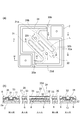
- FIG. 1 It is a top view of the photodetector of one embodiment. It is a top view of the pixel part of the photodetector of FIG. It is a perspective view of the photon detection element of the pixel part of FIG. It is a top view of the photon detection element of FIG. It is sectional drawing of the photon detection element of FIG. It is a figure which shows the principle of an optical resonant structure. It is a figure which shows the manufacturing method of the photodetector of FIG. It is a figure which shows the manufacturing method of the photodetector of FIG. It is a figure which shows the manufacturing method of the photodetector of FIG. It is a figure which shows the manufacturing method of the photodetector of FIG. It is a figure which shows the manufacturing method of the photodetector of FIG.
- the photodetector 1 shown in FIG. 1 detects light by using a function as a bolometer.
- the light is, for example, infrared.
- the photodetector 1 is used for an infrared imager, thermography, or the like.
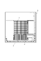
- the photodetector 1 includes a substrate 2, a pixel unit 3, and a signal processing circuit unit 4.
- the substrate 2 is, for example, a Si substrate.
- the thickness of the substrate 2 is, for example, about several hundred ⁇ m.
- the pixel unit 3 and the signal processing circuit unit 4 are formed on the substrate 2 and are electrically connected to each other. Note that the signal processing circuit unit 4 may be formed in the substrate 2.
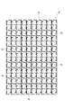
- the pixel unit 3 includes a plurality of light detection elements 10.
- the plurality of light detection elements 10 are arranged in a two-dimensional matrix.
- the light detection element 10 includes a substrate 2 (more precisely, a part of the substrate 2), a light reflection layer 5, a pair of electrode plugs 11 and 12, and a film body 20. I have.
- the light reflecting layer 5 is formed on the surface 2 a of the substrate 2.
- the light reflection layer 5 faces a light absorption layer 34 described later, and constitutes an optical resonance structure together with the light absorption layer 34.
- the thickness of the light reflection layer 5 is, for example, about several hundred nm.
- the material of the light reflection layer 5 is, for example, a metal material (for example, Al) having a high reflectance with respect to light (for example, infrared rays).
- the pair of electrode plugs 11 and 12 are formed on the surface 2 a of the substrate 2.
- Each of the electrode plugs 11 and 12 is formed in a cylindrical shape, for example.
- the height of each electrode plug 11, 12 is, for example, about several ⁇ m.
- the material of each electrode plug 11, 12 is a metal material such as Ti, for example.
- the pair of electrode plugs 11 and 12 support the film body 20 on the surface 2 a of the substrate 2 so that a gap S is formed between the surface 2 a of the substrate 2 and the film body 20.
- the film body 20 is disposed substantially parallel to the surface 2 a of the substrate 2.
- the distance between the film body 20 and the surface 2a of the substrate 2 is, for example, about several ⁇ m.
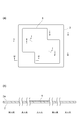
- the film body 20 includes a light receiving portion 21, a pair of electrode portions 22 and 23, and a pair of beam portions 24 and 25.
- the light receiving portion 21 extends so as to avoid the electrode plugs 11 and 12 when viewed from the thickness direction of the substrate 2 (that is, the direction perpendicular to the surface 2a of the substrate 2).
- the electrode portion 22 is disposed on the electrode plug 11.
- the electrode part 23 is disposed on the electrode plug 12.
- the beam portion 24 extends along the outer edge of the light receiving portion 21 on one side of the light receiving portion 21.
- the beam portion 25 extends along the outer edge of the light receiving portion 21 on the other side of the light receiving portion 21.
- the film body 20 has, for example, a rectangular shape when viewed from the thickness direction of the substrate 2.
- the pair of electrode portions 22 and 23 is provided at each diagonal of the film body 20.
- the light receiving portion 21, the pair of electrode portions 22, 23, and the pair of beam portions 24, 25 are integrally formed.
- a slit 20 a is formed continuously between the light receiving unit 21 and the electrode unit 22 and between the light receiving unit 21 and the beam unit 24.
- Slits 20b are continuously formed between the light receiving unit 21 and the electrode unit 23 and between the light receiving unit 21 and the beam unit 25.
- the width of each beam portion 24, 25 is, for example, about several ⁇ m, and the length of each beam portion 24, 25 is, for example, about several tens of ⁇ m.
- the width of each slit 20a, 20b is, for example, about several ⁇ m.
- FIG. 5 is a cross-sectional view of the light detection element 10.
- II, II-II, III-III, IV-IV, and VV in FIG. 5 are the lines II, II-II, III-III, IV-IV, and V, respectively, in FIG.
- FIG. 6 is a cross-sectional view taken along the line V.
- the film body 20 includes a first wiring layer 31 and a second wiring layer 32, a resistance layer 33, a light absorption layer 34, and a separation layer 35.
- the first wiring layer 31 and the second wiring layer 32 face each other through the gap G in the light receiving unit 21. Yes.
- the gap G extends along the line L.
- the line L extends in a meandering manner so as to connect, for example, the electrode portion 22 and the electrode portion 23.
- the line L has a meandering portion L1.
- the meandering portion L1 includes a plurality of curved portions L2.
- the meandering portion L1 extends to one side of the light receiving portion 21 in the light receiving portion 21, turns back, for example, 180 ° at the curved portion L2, extends to the other side of the light receiving portion 21, and turns back, for example, 180 ° at the curved portion L2. Thus, it is configured by repeatedly extending to one side of the light receiving unit 21 again.
- one side is one side with respect to a straight line connecting the electrode part 22 and the electrode part 23 when viewed from the thickness direction of the substrate 2 (for example, the side where the beam part 24 exists).
- the other side is the side opposite to one side with respect to the straight line connecting the electrode part 22 and the electrode part 23 when viewed from the thickness direction of the substrate 2 (for example, the beam part 25 exists) Side).
- one side is one side (for example, the side where the beam portion 24 exists) with respect to a straight line passing through the center of gravity of the film body 20 when viewed from the thickness direction of the substrate 2, and the other side.
- one side refers to the first region 34 a side in the light absorption layer 34
- the other side refers to the second region 34 b side in the light absorption layer 34.
- the meandering portion L1 When viewed from the thickness direction of the substrate 2, the meandering portion L1 includes a first section L3, a second section L4, a third section L5, and a fourth section L6.
- the first section L3 swings to one side with the first swing amount.
- the second section L4 swings to one side with the second swing amount.
- the second section L ⁇ b> 4 When viewed from the thickness direction of the substrate 2, the second section L ⁇ b> 4 is sandwiched between the two first sections L ⁇ b> 3 in the direction along the straight line connecting the electrode section 22 and the electrode section 23.
- the third section L5 swings to the other side with the first swing amount.
- the fourth section L6 swings to the other side by the second swing amount.
- the fourth section L6 When viewed from the thickness direction of the substrate 2, the fourth section L6 is sandwiched between the two third sections L5 in the direction along the straight line connecting the electrode section 22 and the electrode section 23.
- the first shake amount is larger than the predetermined amount.
- the second shake amount is smaller than the predetermined amount.
- the first shake amount is, for example, about ten and several ⁇ m.
- the second shake amount is, for example, about several ⁇ m.
- the first section L ⁇ b> 3 extends to the first deflection amount on one side of the light receiving unit 21, and is folded, for example, by 180 ° at the curved portion L ⁇ b> 2, and the first section L ⁇ b> 3 is on the other side of the light receiving unit 21.
- the fourth section L6 extends the second deflection amount to the other side of the light receiving portion 21 and turns back, for example, 180 ° at the curved portion L2, and extends the second deflection amount to one side of the light receiving portion 21. Yes.
- the second section L4 extends a second deflection amount to one side of the light receiving portion 21 and turns back, for example, 180 ° at the curved portion L2, and extends a second deflection amount to the other side of the light receiving portion 21.
- the third section L5 extends the first deflection amount to the other side of the light receiving portion 21 and turns back, for example, 180 ° at the curved portion L2, and extends to the one side of the light receiving portion 21.
- the meandering portion L1 is configured by repeating such operations.
- Each of the first section L3, the second section L4, the third section L5, and the fourth section L6 includes a curved portion L2.
- the first wiring layer 31 and the second wiring layer 32 are elongated in the direction along the line L in the light receiving unit 21. That is, when viewed from the thickness direction of the substrate 2, the lengths of the first wiring layer 31 and the second wiring layer 32 in the direction along the line L in the light receiving unit 21 are directions perpendicular to the line L. The width of each of the first wiring layer 31 and the second wiring layer 32 is larger.
- the direction perpendicular to the line L refers to a direction perpendicular to the tangent at each position of the line L when viewed from the thickness direction of the substrate 2. At each position of the curved portion, the direction perpendicular to the line L is different.
- the first wiring layer 31 has a first edge 31 a and a third edge 31 b in the light receiving part 21.
- each of the first edge portion 31 a and the third edge portion 31 b extends along the line L.
- the first edge portion 31a extends on the line L side.
- the third edge portion 31b extends on the side opposite to the line L.
- the second wiring layer 32 has a second edge portion 32 a and a fourth edge portion 32 b in the light receiving unit 21.
- each of the second edge portion 32 a and the fourth edge portion 32 b extends along the line L.
- the second edge portion 32a extends on the line L side.
- the fourth edge portion 32b extends on the side opposite to the line L.
- the first edge portion 31 a and the second edge portion 32 a are opposed to each other via the line L. That is, when viewed from the thickness direction of the substrate 2, the gap G is defined by the first edge portion 31a and the second edge portion 32a.
- the second edge 32a on the L side and the fourth edge 32b on the side opposite to the line L respectively extend continuously.
- the term “the edge extends continuously” means that the edge does not have a corner and is formed smoothly. That is, the continuously extending edge portion does not include a portion having an infinitesimal radius of curvature.
- the minimum value of the curvature radius of each of the first edge portion 31a, the second edge portion 32a, the third edge portion 31b, and the fourth edge portion 32b is greater than 0.01 ⁇ m.
- each length of the first wiring layer 31 and the second wiring layer 32 in the direction along the line L in the light receiving unit 21 is, for example, several tens to several hundreds ⁇ m. Degree.
- the widths of the first wiring layer 31 and the second wiring layer 32 in the direction perpendicular to the line L are, for example, about several ⁇ m.
- the width of the gap G in the direction perpendicular to the line L is, for example, about several ⁇ m.
- the thickness of the first wiring layer 31 and the second wiring layer 32 is, for example, about several tens to several hundreds nm.
- the first wiring layer 31 extends from the light receiving portion 21 to the electrode portion 22 via the beam portion 24.
- the first wiring layer 31 is formed on the electrode plug 11 in the electrode portion 22.
- the first wiring layer 31 is electrically connected to the electrode plug 11.
- the second wiring layer 32 extends from the light receiving portion 21 to the electrode portion 23 via the beam portion 25.
- the second wiring layer 32 is formed on the electrode plug 12 in the electrode portion 23.
- the second wiring layer 32 is electrically connected to the electrode plug 12.
- the material of the first wiring layer 31 and the second wiring layer 32 is, for example, a metal material such as Ti.
- the resistance layer 33 is formed in the light receiving unit 21 so as to cover the first wiring layer 31 and the second wiring layer 32 from the opposite side of the substrate 2.
- the resistance layer 33 includes a surface on the opposite side of the substrate 2 in each of the first wiring layer 31 and the second wiring layer 32, and a side surface of each of the first wiring layer 31 and the second wiring layer 32. Covering. That is, the resistance layer 33 is disposed in the gap G.
- the resistance layer 33 is formed on the surfaces of the first wiring layer 31 and the second wiring layer 32 on the opposite side of the substrate 2 in the electrode portions 22 and 23 and the beam portions 24 and 25.
- the resistance layer 33 is electrically connected to each of the first wiring layer 31 and the second wiring layer 32.
- the thickness of the resistance layer 33 is, for example, about several tens to several hundreds nm.
- the resistance layer 33 has an electrical resistance that depends on temperature.
- the material of the resistance layer 33 is a material having a large change in electrical resistivity due to a temperature change, such as amorphous silicon (a-Si).
- the light absorption layer 34 faces the surface 2 a of the substrate 2 in the light receiving unit 21.
- the light absorption layer 34 is disposed on the opposite side of the substrate 2 with respect to the resistance layer 33. When viewed from the thickness direction of the substrate 2, the light absorption layer 34 extends over almost the entire region of the light receiving unit 21.
- the thickness of the light absorption layer 34 is, for example, about a dozen nm.
- the material of the light absorption layer 34 is, for example, WSi 2 or Ti.
- the separation layer 35 is disposed between each of the first wiring layer 31 and the second wiring layer 32 and the light absorption layer 34. Specifically, the separation layer 35 is formed on the surface of the resistance layer 33 opposite to the substrate 2 in the light receiving portion 21, the beam portions 24 and 25, and the electrode portions 22 and 23.
- the light absorption layer 34 is formed on the surface of the light receiving unit 21 opposite to the substrate 2 of the separation layer 35.
- the thickness of the separation layer 35 is, for example, about several hundred nm. The thickness of the separation layer 35 is larger than the thickness of each of the first wiring layer 31, the second wiring layer 32, the resistance layer 33, and the light absorption layer 34.
- the material of the separation layer 35 is, for example, a silicon nitride film (SiN).
- the light absorbing layer 34 When viewed from the thickness direction of the substrate 2, the light absorbing layer 34 includes a first region 34a and a second region 34b.
- the first region 34 a extends to the opposite side of the second wiring layer 32 with respect to the first wiring layer 31 when viewed from the thickness direction of the substrate 2.
- the second region 34 b extends to the opposite side of the first wiring layer 31 with respect to the second wiring layer 32 when viewed from the thickness direction of the substrate 2.
- the total area of the first wiring layer 31 and the second wiring layer 32 is smaller than the area of each of the first region 34a and the second region 34b.
- the first region 34 a and the second region 34 b of the light absorption layer 34 are formed on the resistance layer 33 with the separation layer 35 interposed therebetween.
- each of the resistance layer 33 and the separation layer 35 is continuously formed across the first region 34a and the second region 34b.
- the film body 20 has through holes 20c and 20d.
- the through holes 20c and 20d are holes through which an etching gas for removing a sacrificial layer 6 described later passes.
- the through holes 20c and 20d are formed on one side of the second section L4. Specifically, the through hole 20c is located between the two first sections L3 in the first region 34a.
- the through hole 20d is located between the two third sections L5 in the second region 34b.
- the through holes 20c and 20d have a circular shape, and the diameter thereof is, for example, about several ⁇ m.
- light is detected as follows. First, when light is incident on the light receiving unit 21, heat is generated in a light absorption layer 34 constituting an optical resonance structure described later. At this time, the light receiving unit 21 and the substrate 2 are thermally separated by the gap S. The light receiving unit 21, the electrode unit 22, and the beam unit 24 are thermally separated by the slit 20a. The light receiving unit 21, the electrode unit 23, and the beam unit 25 are thermally separated by the slit 20b. For this reason, the heat generated in the light absorption layer 34 is prevented from escaping to the substrate 2 side via the beam portions 24 and 25 and the electrode portions 22 and 23.
- the heat generated in the light absorption layer 34 is transmitted to the resistance layer 33 through the separation layer 35.
- the resistance layer 33 increases in temperature and increases in electrical resistance due to this heat.
- Such a change in electrical resistance is sent as a signal to the signal processing circuit unit 4 via the first wiring layer 31 and the second wiring layer 32 electrically connected to the resistance layer 33 and the electrode plugs 11 and 12. It is done.
- the change in the electrical resistance of the resistance layer 33 is converted into a change in voltage or current, and light is detected based on the change in voltage or current.
- part of incident light A (having a wavelength of ⁇ ) incident on the light absorption layer 34 is reflected by the light absorption layer 34 as reflected light B1, and the other part is light absorption layer. 34 is transmitted. Another part of the incident light A that has passed through the light absorption layer 34 is reflected by the light reflection layer 5 as reflected light B2. Then, the reflected light B1 and the reflected light B2 interfere with each other on the reflecting surface of the light absorption layer 34 and cancel each other. Thereby, the incident light A is absorbed by the reflection surface of the light absorption layer 34. Heat is generated in the light absorption layer 34 by the energy of the absorbed incident light A.
- the absorption rate of the incident light A is determined by the sheet resistance of the light absorption layer 34 and the optical distance t between the light absorption layer 34 and the light reflection layer 5.
- the thickness of the light absorption layer 34 is set to about 16 nm (when the material of the light absorption layer 34 is WSi 2 ) so that the sheet resistance becomes a vacuum impedance (377 ⁇ / sq). According to this, the amplitude of the reflected light B ⁇ b> 1 reflected by the light absorbing layer 34 matches the amplitude of the reflected light B ⁇ b> 2 reflected by the light reflecting layer 5. For this reason, the reflected light B1 and the reflected light B2 efficiently interfere and cancel each other on the reflecting surface of the light absorption layer 34. Therefore, the absorption rate of the incident light A is improved.
- the light reflection layer 5 forms an optical resonance structure with the light absorption layer 34. When viewed from the thickness direction of the substrate 2, the larger the area of the overlapping portion of the light reflecting layer 5 and the light absorbing layer 34, the more efficiently the incident light A is absorbed.
- the gap G between the first wiring layer 31 and the second wiring layer 32 extends along the line L including the curved portion L2. .
- a sensitivity improves.
- the first edge 31 a on the line L side in the first wiring layer 31 and the second edge 32 a on the line L side in the second wiring layer 32 respectively extend continuously.
- Sensitivity refers to the ability of the photodetector 1 to detect light. For example, when the photodetector 1 can detect even weak light, the sensitivity of the photodetector 1 is high, and when the photodetector 1 cannot detect even strong light, The sensitivity is low.
- the response speed refers to a rate of change of the temperature of the film body 20 with respect to time when light (for example, light amount) incident on the light receiving unit 21 changes. For example, if the time taken for the temperature of the film body 20 to rise to a predetermined stable temperature is short when the amount of light incident on the light receiving unit 21 is increased, the response speed is said to be fast. If it is long, the response speed is low.
- each of the first wiring layer 31 and the second wiring layer 32 is formed in the light receiving unit 21 so as to cross the light receiving unit 21.
- the line L has a meandering portion L1 including a curved portion L2. According to this configuration, the length of the gap G can be lengthened and the sensitivity can be further improved.
- the meandering portion L1 swings to one side with a first section L3 that swings to one side with a first swing amount that is larger than a predetermined amount and a second swing amount that is smaller than a predetermined amount.
- Through-holes 20c and 20d located on one side of the second section L4 are formed in the film body 20 including the second section L4. According to this configuration, the positions of the through holes 20c and 20d can be brought closer to the center of the film body 20 while preventing the through holes 20c and 20d from penetrating the film body 20 in the gap G. Therefore, in the manufacturing process of the photodetector 1, the film body 20 can be efficiently formed by performing the etching through the through holes 20c and 20d.
- the second section L4 is sandwiched between the two first sections L3, and the through holes 20c and 20d are positioned between the two first sections L3.
- the positions of the through holes 20c and 20d can be brought closer to the center of the film body 20 while preventing the through holes 20c and 20d from penetrating the film body 20 in the gap G. Therefore, in the manufacturing process of the photodetector 1, the film body 20 can be efficiently formed by performing the etching through the through holes 20c and 20d.
- the light absorption layer 34 faces the surface 2 a of the substrate 2, and the separation layer 35 is interposed between each of the first wiring layer 31 and the second wiring layer 32 and the light absorption layer 34. Is arranged.
- the first region 34 a of the light absorption layer 34 extends to the opposite side of the second wiring layer 32 with respect to the first wiring layer 31 when viewed from the thickness direction of the substrate 2, and the second region of the light absorption layer 34
- the region 34 b extends to the opposite side of the first wiring layer 31 with respect to the second wiring layer 32 when viewed from the thickness direction of the substrate 2.
- the first region 34 a of the light absorption layer 34 does not overlap the first wiring layer 31, and the second region 34 b of the light absorption layer 34 is the second wiring layer 32. Does not overlap. Thereby, sufficient light absorption is realized in the first region 34 a and the second region 34 b of the light absorption layer 34.
- a separation layer 35 is disposed between each of the first wiring layer 31 and the second wiring layer 32 and the light absorption layer 34. As a result, the heat generated in the light absorption layer 34 is suppressed from escaping to the substrate 2 side through the first wiring layer 31 and the second wiring layer 32, and the heat is suppressed via the separation layer 35. Communicate enough. As described above, according to this configuration, it is possible to further improve the sensitivity. Further, since the separation layer 35 is disposed between each of the first wiring layer 31 and the second wiring layer 32 and the light absorption layer 34, the film body 20 is hardly warped.
- the 3rd edge part 31b on the opposite side to the line L in the 1st wiring layer 31 and the 4th edge part 32b on the opposite side to the line L in the 2nd wiring layer 32 are continuous. It is extended. According to this configuration, even if the thickness of the film body 20 is reduced to improve the response speed, the third edge 31b and the fourth edge in addition to the first edge 31a and the second edge 32a. In 32b, generation
- the photodetector 1 further includes a light reflection layer 5 disposed on the surface 2a of the substrate 2 and constituting a light absorption layer 34 and an optical resonance structure. According to this configuration, light absorption can be realized in a wavelength region corresponding to the distance between the light absorption layer 34 and the light reflection layer 5.
- the total area of the first wiring layer 31 and the second wiring layer 32 is the respective area of the first region 34a and the second region 34b. Smaller than. According to this configuration, more sufficient light absorption is realized in the first region 34 a and the second region 34 b of the light absorption layer 34, and heat generated in the light absorption layer 34 is generated by the first wiring layer 31 and the second wiring. Since the escape to the substrate 2 side through the layer 32 is further suppressed, the sensitivity can be further improved.
- the lengths of the first wiring layer 31 and the second wiring layer 32 in the direction along the line L are perpendicular to the line L when viewed from the thickness direction of the substrate 2. It is larger than the width of each of the first wiring layer 31 and the second wiring layer 32 in the direction. According to this configuration, the length of the gap G can be lengthened and the sensitivity can be further improved.
- the first region 34 a and the second region 34 b of the light absorption layer 34 are formed on the resistance layer 33 via the separation layer 35. Further, each of the resistance layer 33 and the separation layer 35 is continuously formed across the first region 34a and the second region 34b. According to this configuration, deformation and warpage of the film body 20 can be suppressed, and the manufacturing process of the photodetector 1 can be simplified.
- FIGS. 7 to 15 are the II line and II-II line in (a), respectively.
- FIG. 4 is a cross-sectional view taken along line III-III, line IV-IV, line VV.
- the substrate 2 is prepared, and the light reflecting layer 5 is formed on the surface 2 a of the substrate 2.
- the light reflection layer 5 is formed into the above-described shape (for example, the same shape as the light absorption layer 34) by etching.
- a sacrificial layer 6 is formed on the surface 2 a of the substrate 2 so as to cover the light reflecting layer 5.
- the material of the sacrificial layer 6 is, for example, polyimide.
- through holes 6 a and 6 b are formed in the sacrificial layer 6 by removing a part of the sacrificial layer 6 by etching. In each through-hole 6a, 6b, the surface 2a of the substrate 2 is exposed.
- the electrode plug 11 is formed in the through hole 6a and the electrode plug 12 is formed in the through hole 6b.
- the first wiring layer 31 and the second wiring layer 32 are formed on the sacrificial layer 6.
- the first wiring layer 31 and the second wiring layer 32 are formed in the shape described above by etching.
- a resistance layer 33 is formed on the sacrificial layer 6 so as to cover the first wiring layer 31 and the second wiring layer 32, and further, a separation layer 35 is formed on the resistance layer 33. To do.
- a light absorption layer 34 is formed on the separation layer 35.
- the light absorption layer 34 is formed in the shape described above by etching.
- slits 20a and 20b and through holes 20c and 20d are formed.
- the slits 20a and 20b and the through holes 20c and 20d are formed at the positions described above by etching.
- the etching proceeds from the slits 20 a and 20 b and the through holes 20 c and 20 d to remove the sacrificial layer 6, thereby forming the void S.
- the meandering portion L1 has a first section L3 that swings to one side with a first shake amount that is larger than a predetermined amount, and a second section that swings to one side with a second shake amount that is smaller than the predetermined amount.
- the through hole 20c, 20d located in the one side of the 2nd area L4 is formed in the film body 20 including the area L4. According to this configuration, the positions of the through holes 20c and 20d can be brought closer to the center of the film body 20 while preventing the through holes 20c and 20d from penetrating the film body 20 in the gap G. Therefore, in the manufacturing process of the photodetector 1, the film body 20 can be efficiently formed by performing the etching through the through holes 20c and 20d.
- the film body 20 has an example of a rectangular shape when viewed from the thickness direction of the substrate 2, but is not limited thereto.
- the film body 20 may have various shapes such as a circular shape when viewed from the thickness direction of the substrate 2.
- the first wiring layer 31 extends over almost the entire region of the first region 34a, and the second wiring layer 32 extends over substantially the entire region of the second region 34b.
- each of the third edge 31 b of the first wiring layer 31 and the fourth edge 32 b of the second wiring layer 32 may overlap with the outer edge of the light receiving unit 21.
- substrate 2 showed the example which corresponded, the 1st wiring layer 31 and the 2nd wiring in the thickness direction of the board
- the resistance layer 33 may not be formed in, for example, the electrode portions 22 and 23, the beam portions 24 and 25, the region corresponding to the first region 34a, and the region corresponding to the second region 34b.
- the separation layer 35 may not be disposed in, for example, the electrode portions 22 and 23, the beam portions 24 and 25, the region corresponding to the first region 34a, and the region corresponding to the second region 34b. Further, the thickness of the separation layer 35 may be equal to or less than the thickness of each of the first wiring layer 31, the second wiring layer 32, the resistance layer 33, and the light absorption layer 34. Further, the material of the separation layer 35 may be the same as that of the resistance layer 33.
- the total area of the first wiring layer 31 and the second wiring layer 32 may be smaller than the total area of the first region 34 a and the second region 34 b. . According to this configuration, as described above, more sufficient light absorption is realized in the first region 34a and the second region 34b of the light absorption layer 34, and heat generated in the light absorption layer 34 is generated by the first wiring layer. Since the escape to the substrate 2 side through the first wiring layer 31 and the second wiring layer 32 is further suppressed, the sensitivity can be further improved.
- the separation layer 35 and the light absorption layer 34 may be formed on the substrate 2 side of the first wiring layer 31 and the second wiring layer 32. Specifically, the separation layer 35 is formed on the electrode plugs 11 and 12. The first wiring layer 31, the second wiring layer 32, and the resistance layer 33 are formed on the surface of the separation layer 35 on the opposite side of the substrate 2. The light absorption layer 34 is formed on the surface of the separation layer 35 on the substrate 2 side. According to this, the light absorption layer 34 and the light reflection layer 5 are directly opposed via the gap S. For this reason, the adjustment of the optical distance t is facilitated, and light can be more reliably absorbed by the optical resonance structure. Also in this case, the first wiring layer 31 is electrically connected to the electrode plug 11. The second wiring layer 32 is electrically connected to the electrode plug 12.
- the film body 20 may not have the separation layer 35.
- the resistance layer 33 also functions as both the resistance layer 33 and the separation layer 35. According to this, since the thermal conductance of the film body 20 is lowered, the response speed can be improved. Moreover, according to this, since the element resistance of the film body 20 becomes low, noise can be reduced.
- the resistance layer 33 may be formed on the substrate 2 side of the first wiring layer 31 and the second wiring layer 32. At this time, the resistance layer 33 is not disposed in the gap G. Also in this case, the first wiring layer 31 is electrically connected to the electrode plug 11. The second wiring layer 32 is electrically connected to the electrode plug 12.
- the resistance layer 33, the separation layer 35, and the light absorption layer 34 may be formed on the substrate 2 side of the first wiring layer 31 and the second wiring layer 32.
- the separation layer 35 is formed on the electrode plugs 11 and 12.
- the resistance layer 33 is formed on the surface of the separation layer 35 opposite to the substrate 2.
- the first wiring layer 31 and the second wiring layer 32 are formed on the surface of the resistance layer 33 opposite to the substrate 2.
- the light absorption layer 34 is formed on the surface of the separation layer 35 on the substrate 2 side.
- the first wiring layer 31 is electrically connected to the electrode plug 11.
- the second wiring layer 32 is electrically connected to the electrode plug 12.
- the resistance layer 33 and the light absorption layer 34 are formed on the substrate 2 side of the first wiring layer 31 and the second wiring layer 32, the first wiring layer 31 and the second wiring layer 32 and the light absorption layer are absorbed. If the resistance layer 33 is formed between the layer 34 and the layer 34, the film body 20 may not have the separation layer 35. That is, even in this case, the resistance layer 33 also functions as both the resistance layer 33 and the separation layer 35. Also in this case, the first wiring layer 31 is electrically connected to the electrode plug 11. The second wiring layer 32 is electrically connected to the electrode plug 12.
- the material of the light absorption layer 34 may be a material having a large absorption rate with respect to light, such as black resin.
- the optical resonance structure is not configured, and light is directly absorbed by the light absorption layer 34. According to this, as described above, it is not necessary to adjust the optical distance t with high accuracy.
- the light detection element 10 preferably includes the light reflection layer 5. The reason is as follows. When a part of the incident light A incident on the light absorption layer 34 is not absorbed by the light absorption layer 34 and passes through the film body 20, the incident light A transmitted through the film body 20 is reflected by the light reflection layer 5. Then, it enters the light absorption layer 34 again.
- the incident light A incident on the light absorption layer 34 again is absorbed by the light absorption layer 34 and becomes heat. Thereby, the light absorption rate is improved.
- the material of the light absorption layer 34 is a black resin
- the light absorption layer 34 comes into contact with the resistance layer 33 by disposing the separation layer 35 between the light absorption layer 34 and the resistance layer 33. Thus, the influence on the characteristics of the resistance layer 33 is suppressed.
- the separation layer 35 may be further formed on the surface of the film body 20 on the substrate 2 side. According to this, the resistance layer 33 can be stabilized and the film body 20 can be made more difficult to warp.
- first wiring layer 31 and the second wiring layer 32, the resistance layer 33, the light absorption layer 34, and the separation layer 35 various materials and thicknesses can be applied to the first wiring layer 31 and the second wiring layer 32, the resistance layer 33, the light absorption layer 34, and the separation layer 35, respectively.
- the sensitivity can be easily improved and the strength of the film body 20 can be increased. Can be improved.
- each of the first wiring layer 31, the second wiring layer 32, and the light absorption layer 34 is optimal. By selecting a suitable material, it is possible to achieve both improvement in sensitivity and response speed.
- the through holes 20c and 20d may have various shapes such as an ellipse or a quadrangle.
- the pixel unit 3 may be configured by one photodetecting element 10.
Landscapes
- Physics & Mathematics (AREA)
- General Physics & Mathematics (AREA)
- Spectroscopy & Molecular Physics (AREA)
- Engineering & Computer Science (AREA)
- Manufacturing & Machinery (AREA)
- Chemical & Material Sciences (AREA)
- Nanotechnology (AREA)
- Photometry And Measurement Of Optical Pulse Characteristics (AREA)
- Solid State Image Pick-Up Elements (AREA)
- Light Receiving Elements (AREA)
Abstract
光検出器は、基板と、基板の表面との間に空隙が形成されるように基板の表面上に支持された膜体と、を備え、膜体は、曲線部を含むラインに沿って延在するギャップを介して互いに対向する第1配線層及び第2配線層と、第1配線層及び第2配線層のそれぞれと電気的に接続され、温度に依存する電気抵抗を有する抵抗層と、を有し、第1配線層におけるライン側の第1縁部及び第2配線層におけるライン側の第2縁部は、それぞれ、連続的に延在している。
Description
本発明の一側面は、光検出器に関する。
光検出器として、基板と、基板の表面との間に空隙が形成されるように基板の表面上に支持された膜体と、を備え、膜体が、ギャップを介して互いに対向する一対の配線層と、温度に依存する電気抵抗を有する抵抗層と、を有するものが知られている(例えば、特許文献1参照)。特許文献1に記載された赤外線センサでは、一対の配線層に相当する一対の電極間のギャップが矩形波状に延在している。
特許文献1に記載された赤外線センサでは、一対の電極間のギャップが矩形波状に延在しているため、当該ギャップが直線状に延在している場合に比べ、感度が向上し得る。しかし、特許文献1に記載された赤外線センサにおいて、応答速度の向上のために膜体の厚さが小さくされると、膜体の変形に起因して、矩形波状に延在するギャップの角部において応力集中が生じ易くなり、センサとしての特性が劣化するおそれがある。
そこで、本発明の一側面は、感度及び応答速度の向上を図ることができる光検出器を提供することを目的とする。
本発明の一側面に係る光検出器は、基板と、基板の表面との間に空隙が形成されるように基板の表面上に支持された膜体と、を備え、膜体は、曲線部を含むラインに沿って延在するギャップを介して互いに対向する第1配線層及び第2配線層と、第1配線層及び第2配線層のそれぞれと電気的に接続され、温度に依存する電気抵抗を有する抵抗層と、を有し、第1配線層におけるライン側の第1縁部及び第2配線層におけるライン側の第2縁部は、それぞれ、連続的に延在している。
この光検出器では、第1配線層と第2配線層との間のギャップが、曲線部を含むラインに沿って延在している。これにより、当該ギャップが直線状に延在している場合に比べ、感度が向上する。また、第1配線層におけるライン側の第1縁部及び第2配線層におけるライン側の第2縁部が、それぞれ、連続的に延在している。これにより、応答速度の向上のために膜体の厚さが小さくされたとしても、第1縁部及び第2縁部において、膜体の変形に起因する応力集中の発生が抑制される。以上により、この光検出器によれば、感度及び応答速度の向上を図ることができる。
本発明の一側面に係る光検出器では、ラインは、曲線部を含む蛇行部を有してもよい。この構成によれば、ギャップの長さをより長くし、より一層の感度の向上を図ることができる。
本発明の一側面に係る光検出器では、蛇行部は、所定量よりも大きい第1振れ量で一方の側に振れる第1区間、及び、所定量よりも小さい第2振れ量で一方の側に振れる第2区間を含み、膜体には、第2区間の一方の側に位置する貫通孔が形成されていてもよい。この構成によれば、貫通孔がギャップにおいて膜体を貫通することを防止しつつ、貫通孔の位置を膜体の中央部に近づけることができる。したがって、光検出器の製造工程において、貫通孔を介してエッチングを実施することで、膜体を効率良く形成することができる。
本発明の一側面に係る光検出器では、第2区間は、2つの第1区間によって挟まれており、貫通孔は、2つの第1区間の間に位置していてもよい。この構成によれば、貫通孔がギャップにおいて膜体を貫通することを防止しつつ、貫通孔の位置を膜体の中央部に近づけることができる。したがって、光検出器の製造工程において、貫通孔を介してエッチングを実施することで、膜体を効率良く形成することができる。
本発明の一側面に係る光検出器では、膜体は、基板の表面と対向する光吸収層と、第1配線層及び第2配線層のそれぞれと光吸収層との間に配置された分離層と、を更に有し、光吸収層は、基板の厚さ方向から見た場合に第1配線層に対して第2配線層の反対側に広がる第1領域と、基板の厚さ方向から見た場合に第2配線層に対して第1配線層の反対側に広がる第2領域と、を含んでもよい。この構成では、基板の厚さ方向から見た場合に、光吸収層の第1領域が第1配線層に対して第2配線層の反対側に広がっており、光吸収層の第2領域が第2配線層に対して第1配線層の反対側に広がっている。つまり、基板の厚さ方向から見た場合に、光吸収層の第1領域が第1配線層と重なっておらず、光吸収層の第2領域が第2配線層と重なっていない。これにより、光吸収層の第1領域及び第2領域において十分な光吸収が実現される。しかも、第1配線層及び第2配線層のそれぞれと光吸収層との間に分離層が配置されている。これにより、光吸収層において生じた熱が第1配線層及び第2配線層を伝って基板側に逃げるようなことが抑制され、その熱が分離層を介して抵抗層に十分に伝わる。以上により、この構成によれば、より一層の感度の向上を図ることができる。
本発明の一側面に係る光検出器では、第1配線層におけるラインとは反対側の第3縁部及び第2配線層におけるラインとは反対側の第4縁部は、連続的に延在していてもよい。この構成によれば、応答速度の向上のために膜体の厚さが小さくされたとしても、第1縁部及び第2縁部に加え、第3縁部及び第4縁部において、膜体の変形に起因する応力集中の発生を抑制することができる。
本発明の一側面に係る光検出器は、基板の表面に配置され、光吸収層と光共振構造を構成する光反射層、を更に備えてもよい。この構成によれば、光吸収層と光反射層との距離に応じた波長域において光吸収を実現することができる。
本発明の一側面に係る光検出器では、基板の厚さ方向から見た場合に、第1配線層及び第2配線層の面積の合計は、第1領域及び第2領域の面積の合計よりも小さくてもよい。この構成によれば、光吸収層の第1領域及び第2領域においてより十分な光吸収が実現され、且つ、光吸収層において生じた熱が第1配線層及び第2配線層を伝って基板側に逃げるようなことがより一層抑制されるため、より一層の感度の向上を図ることができる。
本発明の一側面に係る光検出器では、基板の厚さ方向から見た場合に、第1配線層及び第2配線層の面積の合計は、第1領域及び第2領域のそれぞれの面積よりも小さくてもよい。この構成によれば、光吸収層の第1領域及び第2領域においてより十分な光吸収が実現され、且つ、光吸収層において生じた熱が第1配線層及び第2配線層を伝って基板側に逃げるようなことがより一層抑制されるため、より一層の感度の向上を図ることができる。
本発明の一側面に係る光検出器では、基板の厚さ方向から見た場合に、ラインに沿った方向における第1配線層及び第2配線層のそれぞれの長さは、ラインに垂直な方向における第1配線層及び第2配線層のそれぞれの幅よりも大きくてもよい。この構成によれば、ギャップの長さをより長くし、より一層の感度の向上を図ることができる。
本発明の一側面によれば、感度及び応答速度の向上を図ることができる光検出器を提供することが可能となる。
以下、本発明の好適な実施形態について、図面を参照して詳細に説明する。なお、各図において同一又は相当部分には同一符号を付し、重複する説明を省略する。
図1に示される光検出器1は、ボロメータとしての機能を利用することで、光を検出する。当該光は、例えば赤外線である。当該光が赤外線である場合、光検出器1は、赤外イメージャ、又はサーモグラフィー等に用いられる。図1に示されるように、光検出器1は、基板2と、画素部3と、信号処理回路部4と、を備えている。基板2は、例えばSi基板である。基板2の厚さは、例えば数百μm程度である。画素部3及び信号処理回路部4は、基板2上に形成されており、互いに電気的に接続されている。なお、信号処理回路部4は、基板2内に形成されていてもよい。
図2に示されるように、画素部3は、複数の光検出素子10によって構成されている。複数の光検出素子10は、二次元マトリックス状に配置されている。図3に示されるように、光検出素子10は、基板2(正確には、基板2の一部)と、光反射層5と、一対の電極プラグ11,12と、膜体20と、を備えている。
光反射層5は、基板2の表面2aに形成されている。光反射層5は、後述する光吸収層34と対向しており、光吸収層34と共に光共振構造を構成している。光反射層5の厚さは、例えば数百nm程度である。光反射層5の材料は、例えば、光(例えば赤外線)に対する反射率が大きい金属材料(例えばAl等)である。
一対の電極プラグ11,12は、基板2の表面2a上に形成されている。各電極プラグ11,12は、例えば円柱状に形成されている。各電極プラグ11,12の高さは、例えば数μm程度である。各電極プラグ11,12の材料は、例えばTi等の金属材料である。一対の電極プラグ11,12は、基板2の表面2aと膜体20との間に空隙Sが形成されるように、基板2の表面2a上に膜体20を支持している。膜体20は、基板2の表面2aと略平行に配置されている。膜体20と基板2の表面2aとの距離は、例えば数μm程度である。
図3及び図4に示されるように、膜体20は、受光部21と、一対の電極部22,23と、一対の梁部24,25と、を有している。受光部21は、基板2の厚さ方向(すなわち、基板2の表面2aに垂直な方向)から見た場合に、各電極プラグ11,12を避けるように広がっている。電極部22は、電極プラグ11上に配置されている。電極部23は、電極プラグ12上に配置されている。梁部24は、受光部21の一方の側において受光部21の外縁に沿って延在している。梁部25は、受光部21の他方の側において受光部21の外縁に沿って延在している。梁部24の一端は、電極部22と接続されており、梁部24の他端は、電極部23の近傍の位置で受光部21と接続されている。梁部25の一端は、電極部23と接続されており、梁部25の他端は、電極部22の近傍の位置で受光部21と接続されている。膜体20は、基板2の厚さ方向から見た場合に、例えば矩形状を呈している。一対の電極部22,23は、膜体20の対角のそれぞれに設けられている。
受光部21、一対の電極部22,23、及び一対の梁部24,25は、一体的に形成されている。受光部21と電極部22との間、及び受光部21と梁部24との間には、スリット20aが一続きに形成されている。受光部21と電極部23との間、及び受光部21と梁部25との間には、スリット20bが一続きに形成されている。各梁部24,25の幅は、例えば数μm程度であり、各梁部24,25の長さは、例えば数十μm程度である。各スリット20a,20bの幅は、例えば数μm程度である。
図5は、光検出素子10の断面図である。図5のI-I、II-II、III-III、IV-IV、V-Vは、それぞれ、図4のI-I線、II-II線、III-III線、IV-IV線、V-V線に沿っての断面図である。図5に示されるように、膜体20は、第1配線層31及び第2配線層32と、抵抗層33と、光吸収層34と、分離層35と、を有している。
図4及び図5に示されるように、基板2の厚さ方向から見た場合に、第1配線層31及び第2配線層32は、受光部21において、ギャップGを介して互いに対向している。ギャップGは、ラインLに沿って延在している。ラインLは、基板2の厚さ方向から見た場合に、例えば電極部22と電極部23とを結ぶように蛇行状に延在している。具体的には、ラインLは、蛇行部L1を有している。蛇行部L1は、複数の曲線部L2を含んでいる。蛇行部L1は、受光部21において、受光部21の一方の側に延び、曲線部L2において、例えば180°折り返して、受光部21の他方の側に延び、曲線部L2において、例えば180°折り返して、再び受光部21の一方の側に伸びることを繰り返すことによって構成されている。
本実施形態では、一方の側とは、基板2の厚さ方向から見た場合に、電極部22と電極部23とを結ぶ直線に対して一方の側(例えば梁部24が存在する側)をいい、他方の側とは、基板2の厚さ方向から見た場合に、電極部22と電極部23とを結ぶ直線に対して一方の側とは反対の側(例えば梁部25が存在する側)をいう。また、一方の側とは、基板2の厚さ方向から見た場合に、膜体20の重心を通る直線に対して一方の側(例えば梁部24が存在する側)であり、他方の側とは、基板2の厚さ方向から見た場合に、膜体20の重心を通る直線に対して一方の側とは反対の側(梁部25が存在する側)であってもよい。つまり、一方の側とは、光吸収層34における第1領域34a側をいい、他方の側とは、光吸収層34における第2領域34b側をいう。
基板2の厚さ方向から見た場合に、蛇行部L1は、第1区間L3と、第2区間L4と、第3区間L5と、第4区間L6と、を含んでいる。第1区間L3は、第1振れ量で一方の側に振れている。第2区間L4は、第2振れ量で一方の側に振れている。基板2の厚さ方向から見た場合に、電極部22と電極部23とを結ぶ直線に沿った方向において、第2区間L4は2つの第1区間L3によって挟まれている。第3区間L5は、第1振れ量で他方の側に振れている。第4区間L6は、第2振れ量で他方の側に振れている。基板2の厚さ方向から見た場合に、電極部22と電極部23とを結ぶ直線に沿った方向において、第4区間L6は2つの第3区間L5によって挟まれている。第1振れ量は、所定量よりも大きい。第2振れ量は、所定量よりも小さい。第1振れ量は、例えば十数μm程度である。第2振れ量は、例えば数μm程度である。
具体的には、受光部21において、第1区間L3は、受光部21の一方の側に第1振れ量延び、曲線部L2において、例えば180°折り返して、受光部21の他方の側に第1振れ量延びている。これに続いて、第4区間L6は、受光部21の他方の側に第2振れ量延び、曲線部L2において、例えば180°折り返して、受光部21の一方の側に第2振れ量延びている。これに続いて、第2区間L4は、受光部21の一方の側に第2振れ量延び、曲線部L2において、例えば180°折り返して、受光部21の他方の側に第2振れ量延びている。これに続いて、第3区間L5は、受光部21の他方の側に第1振れ量延び、曲線部L2において、例えば180°折り返して、受光部21の一方の側に第1振れ量延びている。蛇行部L1は、このようなことを繰り返すことによって構成されている。なお、第1区間L3、第2区間L4、第3区間L5及び第4区間L6のそれぞれは、曲線部L2を含んでいる。
第1配線層31及び第2配線層32は、受光部21において、ラインLに沿った方向において細長く形成されている。つまり、基板2の厚さ方向から見た場合に、受光部21において、ラインLに沿った方向における第1配線層31及び第2配線層32のそれぞれの長さは、ラインLに垂直な方向における第1配線層31及び第2配線層32のそれぞれの幅よりも大きい。ラインLに垂直な方向とは、基板2の厚さ方向から見た場合に、ラインLの各位置における接線に垂直な方向をいう。曲線部の各位置においては、ラインLに垂直な方向はそれぞれ相違する。
具体的には、第1配線層31は、受光部21において、第1縁部31aと、第3縁部31bと、を有している。基板2の厚さ方向から見た場合に、第1縁部31a及び第3縁部31bのそれぞれは、ラインLに沿って延在している。第1縁部31aは、ラインL側において延在している。第3縁部31bは、ラインLとは反対側において延在している。第2配線層32は、受光部21において、第2縁部32aと、第4縁部32bと、を有している。基板2の厚さ方向から見た場合に、第2縁部32a及び第4縁部32bのそれぞれは、ラインLに沿って延在している。第2縁部32aは、ラインL側において延在している。第4縁部32bは、ラインLとは反対側において延在している。
基板2の厚さ方向から見た場合に、第1縁部31aと第2縁部32aとはラインLを介して互いに対向している。つまり、基板2の厚さ方向から見た場合に、ギャップGは、第1縁部31aと第2縁部32aとによって画定されている。
基板2の厚さ方向から見た場合に、第1配線層31におけるラインL側の第1縁部31a及びラインLとは反対側の第3縁部31b、並びに、第2配線層32におけるラインL側の第2縁部32a及びラインLとは反対側の第4縁部32bは、それぞれ、連続的に延在している。縁部が連続的に延在しているとは、縁部が角部を有しておらず、滑らかに形成されていることをいう。つまり、連続的に延在している縁部は、曲率半径が無限小の部分を含まない。例えば、第1縁部31a、第2縁部32a、第3縁部31b及び第4縁部32bのそれぞれの曲率半径の最小値は、0.01μmよりも大きい。
基板2の厚さ方向から見た場合に、受光部21において、ラインLに沿った方向における第1配線層31及び第2配線層32のそれぞれの長さは、例えば、数十~数百μm程度である。基板2の厚さ方向から見た場合に、ラインLに垂直な方向における第1配線層31及び第2配線層32のそれぞれの幅は、例えば数μm程度である。基板2の厚さ方向から見た場合に、ラインLに垂直な方向におけるギャップGの幅は、例えば数μm程度である。第1配線層31及び第2配線層32の厚さは、例えば数十~数百nm程度である。
第1配線層31は、受光部21から梁部24を介して電極部22に延在している。第1配線層31は、電極部22において電極プラグ11上に形成されている。第1配線層31は、電極プラグ11と電気的に接続されている。第2配線層32は、受光部21から梁部25を介して電極部23に延在している。第2配線層32は、電極部23において電極プラグ12上に形成されている。第2配線層32は、電極プラグ12と電気的に接続されている。第1配線層31及び第2配線層32の材料は、例えばTi等の金属材料である。
抵抗層33は、受光部21においては、基板2の反対側から第1配線層31及び第2配線層32を覆うように形成されている。抵抗層33は、受光部21においては、第1配線層31及び第2配線層32のそれぞれにおける基板2の反対側の表面、並びに、第1配線層31及び第2配線層32のそれぞれの側面を覆っている。つまり、ギャップGには、抵抗層33が配置されている。抵抗層33は、電極部22,23及び梁部24,25においては、第1配線層31及び第2配線層32における基板2の反対側の表面上に形成されている。抵抗層33は、第1配線層31及び第2配線層32のそれぞれと電気的に接続されている。抵抗層33の厚さは、例えば数十~数百nm程度である。抵抗層33は、温度に依存する電気抵抗を有している。抵抗層33の材料は、例えばアモルファスシリコン(a-Si)等の温度変化による電気抵抗率の変化が大きい材料である。
光吸収層34は、受光部21において、基板2の表面2aと対向している。光吸収層34は、抵抗層33に対して基板2の反対側に配置されている。光吸収層34は、基板2の厚さ方向から見た場合に、受光部21のほぼ全領域に広がっている。光吸収層34の厚さは、例えば十数nm程度である。光吸収層34の材料は、例えばWSi2又はTi等である。
分離層35は、第1配線層31及び第2配線層32のそれぞれと光吸収層34との間に配置されている。具体的には、分離層35は、受光部21、梁部24,25及び電極部22,23において、抵抗層33における基板2の反対側の表面上に形成されている。そして、光吸収層34は、受光部21において分離層35の基板2の反対側の表面上に形成されている。分離層35の厚さは、例えば数百nm程度である。分離層35の厚さは、第1配線層31、第2配線層32、抵抗層33及び光吸収層34のそれぞれの厚さよりも大きい。分離層35の材料は、例えばシリコン窒化膜(SiN)等である。
基板2の厚さ方向から見た場合に、光吸収層34は、第1領域34aと、第2領域34bと、を含んでいる。第1領域34aは、基板2の厚さ方向から見た場合に、第1配線層31に対して第2配線層32の反対側に広がっている。第2領域34bは、基板2の厚さ方向から見た場合に、第2配線層32に対して第1配線層31の反対側に広がっている。基板2の厚さ方向から見た場合に、第1配線層31及び第2配線層32の面積の合計は、第1領域34a及び第2領域34bのそれぞれの面積よりも小さい。
なお、光吸収層34の第1領域34a及び第2領域34bは、分離層35を介して抵抗層33上に形成されている。また、抵抗層33及び分離層35のそれぞれは、第1領域34a及び第2領域34bを亘って連続的に形成されている。
膜体20には、貫通孔20c,20dが形成されている。貫通孔20c,20dは、後述する犠牲層6を除去するエッチングガスが通過する孔である。基板2の厚さ方向から見た場合に、貫通孔20c,20dは、第2区間L4の一方の側に形成されている。具体的には、貫通孔20cは、第1領域34aにおいて、2つの第1区間L3の間に位置している。貫通孔20dは、第2領域34bにおいて、2つの第3区間L5の間に位置している。基板2の厚さ方向から見た場合に、貫通孔20c,20dは、円形を呈しており、その直径は、例えば数μm程度である。
以上のように構成された光検出器1では、以下のように、光が検出される。まず、光が受光部21に入射すると、後述する光共振構造を構成する光吸収層34において熱が生じる。このとき、受光部21と基板2とは、空隙Sによって熱的に分離されている。また、受光部21と電極部22及び梁部24とは、スリット20aによって熱的に分離されている。また、受光部21と電極部23及び梁部25とは、スリット20bによって熱的に分離されている。このため、光吸収層34において生じた熱が、梁部24,25及び電極部22,23を介して基板2側に逃げるようなことが抑制される。
光吸収層34において生じた熱は、分離層35を介して抵抗層33に伝わる。そして、抵抗層33は、この熱によって温度が上昇すると共に電気抵抗が上昇する。このような電気抵抗の変化は、信号として抵抗層33と電気的に接続された第1配線層31及び第2配線層32、並びに、電極プラグ11,12を介して信号処理回路部4へ送られる。そして、信号処理回路部4では、抵抗層33の電気抵抗の変化が電圧または電流の変化に変換され、この電圧または電流の変化を基に、光が検出される。
次に、光共振構造について詳細に説明する。図6に示されるように、光吸収層34に入射した入射光A(波長がλである)は、一部が光吸収層34によって反射光B1として反射され、他の一部が光吸収層34を透過する。光吸収層34を透過した入射光Aの他の一部は、光反射層5によって反射光B2として反射される。そして、反射光B1と反射光B2とは、光吸収層34の反射面において、互いに干渉して打ち消される。これにより、光吸収層34の当該反射面において入射光Aが吸収される。吸収された入射光Aのエネルギーによって光吸収層34において熱が生じる。
入射光Aの吸収率は、光吸収層34のシート抵抗、及び、光吸収層34と光反射層5との間の光学距離tによって決められる。光吸収層34の厚さは、シート抵抗が真空インピーダンス(377Ω/sq)となるように略16nm(光吸収層34の材料が、WSi2である場合)に設定されている。これによれば、光吸収層34によって反射された反射光B1の振幅が光反射層5によって反射された反射光B2の振幅と一致する。このため、光吸収層34の反射面において、反射光B1と反射光B2とが効率的に干渉して打ち消される。従って、入射光Aの吸収率が向上される。
また、光学距離tは、t=(2m-1)λ/4(m=1、2、3、・・・)となるように設定されている。これによれば、反射光B1と反射光B2との位相が180°ずれる。このため、光吸収層34の反射面において、反射光B1と反射光B2とが効率的に干渉して打ち消される。従って、入射光Aの吸収率が向上される。このように、光反射層5は、光吸収層34と光共振構造を構成している。基板2の厚さ方向から見た場合に、光反射層5及び光吸収層34の重なっている部分の面積が広ければ広いほど、入射光Aが効率よく吸収される。
以上説明したように、一実施形態の光検出器1では、第1配線層31と第2配線層32との間のギャップGが、曲線部L2を含むラインLに沿って延在している。これにより、当該ギャップGが直線状に延在している場合に比べ、感度が向上する。また、第1配線層31におけるラインL側の第1縁部31a及び第2配線層32におけるラインL側の第2縁部32aが、それぞれ、連続的に延在している。これにより、応答速度の向上のために膜体20の厚さが小さくされたとしても、第1縁部31a及び第2縁部32aにおいて、膜体20の変形に起因する応力集中の発生が抑制される。以上により、この光検出器によれば、感度及び応答速度の向上を図ることができる。感度とは、光検出器1が、光を検出する能力のことをいう。例えば、光検出器1が弱い光でも検出することができる場合は、光検出器1の感度が高いといい、光検出器1が強い光でも検出することができない場合は、光検出器1の感度が低いという。応答速度とは、受光部21に入射する光(例えば光量)が変化した際、膜体20の温度の時間に対する変化率のことをいう。例えば、受光部21に入射した光の光量が増加した際、膜体20の温度が所定の安定した温度まで上昇するまでにかかった時間が短ければ、応答速度が速いといい、かかった時間が長ければ、応答速度が低いという。
また、第1配線層31及び第2配線層32のそれぞれは、受光部21において、受光部21を横切るように形成されている。これにより、膜体20が第1配線層31及び第2配線層32によって確実に支持されているため、第1配線層31及び第2配線層32間の抵抗層33の歪み及び変形を抑制することができる。
また、光検出器1では、ラインLは、曲線部L2を含む蛇行部L1を有している。この構成によれば、ギャップGの長さをより長くし、より一層の感度の向上を図ることができる。
また、光検出器1では、蛇行部L1は、所定量よりも大きい第1振れ量で一方の側に振れる第1区間L3、及び、所定量よりも小さい第2振れ量で一方の側に振れる第2区間L4を含み、膜体20には、第2区間L4の一方の側に位置する貫通孔20c,20dが形成されている。この構成によれば、貫通孔20c,20dがギャップGにおいて膜体20を貫通することを防止しつつ、貫通孔20c,20dの位置を膜体20の中央部に近づけることができる。したがって、光検出器1の製造工程において、貫通孔20c,20dを介してエッチングを実施することで、膜体20を効率良く形成することができる。
また、光検出器1では、第2区間L4が、2つの第1区間L3によって挟まれており、貫通孔20c,20dが、2つの第1区間L3の間に位置している。この構成によれば、貫通孔20c,20dがギャップGにおいて膜体20を貫通することを防止しつつ、貫通孔20c,20dの位置を膜体20の中央部に近づけることができる。したがって、光検出器1の製造工程において、貫通孔20c,20dを介してエッチングを実施することで、膜体20を効率良く形成することができる。
また、光検出器1では、光吸収層34が基板2の表面2aと対向しており、分離層35が第1配線層31及び第2配線層32のそれぞれと光吸収層34との間に配置されている。光吸収層34の第1領域34aは、基板2の厚さ方向から見た場合に第1配線層31に対して第2配線層32の反対側に広がっており、光吸収層34の第2領域34bは、基板2の厚さ方向から見た場合に第2配線層32に対して第1配線層31の反対側に広がっている。つまり、基板2の厚さ方向から見た場合に、光吸収層34の第1領域34aが第1配線層31と重なっておらず、光吸収層34の第2領域34bが第2配線層32と重なっていない。これにより、光吸収層34の第1領域34a及び第2領域34bにおいて十分な光吸収が実現される。しかも、第1配線層31及び第2配線層32のそれぞれと光吸収層34との間に分離層35が配置されている。これにより、光吸収層34において生じた熱が第1配線層31及び第2配線層32を伝って基板2側に逃げるようなことが抑制され、その熱が分離層35を介して抵抗層33に十分に伝わる。以上により、この構成によれば、より一層の感度の向上を図ることができる。また、第1配線層31及び第2配線層32のそれぞれと光吸収層34との間に分離層35が配置されているため、膜体20が反り難くなる。
また、光検出器1では、第1配線層31におけるラインLとは反対側の第3縁部31b及び第2配線層32におけるラインLとは反対側の第4縁部32bは、連続的に延在している。この構成によれば、応答速度の向上のために膜体20の厚さが小さくされたとしても、第1縁部31a及び第2縁部32aに加え、第3縁部31b及び第4縁部32bにおいて、膜体20の変形に起因する応力集中の発生を抑制することができる。
また、光検出器1は、基板2の表面2aに配置され、光吸収層34と光共振構造を構成する光反射層5、を更に備えている。この構成によれば、光吸収層34と光反射層5との距離に応じた波長域において光吸収を実現することができる。
また、光検出器1では、基板2の厚さ方向から見た場合に、第1配線層31及び第2配線層32の面積の合計が、第1領域34a及び第2領域34bのそれぞれの面積よりも小さい。この構成によれば、光吸収層34の第1領域34a及び第2領域34bにおいてより十分な光吸収が実現され、且つ、光吸収層34において生じた熱が第1配線層31及び第2配線層32を伝って基板2側に逃げるようなことがより一層抑制されるため、より一層の感度の向上を図ることができる。
また、光検出器1では、基板2の厚さ方向から見た場合に、ラインLに沿った方向における第1配線層31及び第2配線層32のそれぞれの長さが、ラインLに垂直な方向における第1配線層31及び第2配線層32のそれぞれの幅よりも大きい。この構成によれば、ギャップGの長さをより長くし、より一層の感度の向上を図ることができる。
また、光検出器1では、光吸収層34の第1領域34a及び第2領域34bが、分離層35を介して抵抗層33上に形成されている。また、抵抗層33及び分離層35のそれぞれが、第1領域34a及び第2領域34bを亘って連続的に形成されている。この構成によれば、膜体20の変形及び反りを抑制すると共に、光検出器1の製造プロセスを簡素化することができる。
次に、光検出器1の製造方法について、図7~図15を参照しつつ説明する。図7~図15の各図において、(b)のI-I、II-II、III-III、IV-IV、V-Vは、それぞれ、(a)のI-I線、II-II線、III-III線、IV-IV線、V-V線に沿っての断面図である。
まず、図7に示されるように、基板2を用意し、基板2の表面2aに光反射層5を形成する。光反射層5は、エッチングによって上述した形状(例えば、光吸収層34と同形状)に形成される。続いて、図8に示されるように、光反射層5を覆うように基板2の表面2aに犠牲層6を形成する。犠牲層6の材料は、例えばポリイミド等である。続いて、図9に示されるように、エッチングによって犠牲層6の一部を除去することで、犠牲層6に貫通孔6a,6bを形成する。各貫通孔6a,6bにおいては、基板2の表面2aが露出させられる。
続いて、図10に示されるように、貫通孔6aに電極プラグ11を形成すると共に,貫通孔6bに電極プラグ12を形成する。続いて、図11に示されるように、犠牲層6上に第1配線層31及び第2配線層32を形成する。第1配線層31及び第2配線層32は、エッチングによって上述した形状に形成される。続いて、図12に示されるように、第1配線層31及び第2配線層32を覆うように犠牲層6上に抵抗層33を形成し、更に、抵抗層33上に分離層35を形成する。
続いて、図13に示されるように、分離層35上に光吸収層34を形成する。光吸収層34は、エッチングによって上述した形状に形成される。続いて、図14に示されるように、スリット20a,20b及び貫通孔20c,20dを形成する。スリット20a,20b及び貫通孔20c,20dは、エッチングによって上述した位置に形成される。続いて、図15に示されるように、スリット20a,20b及び貫通孔20c,20dからエッチングを進行させ、犠牲層6を除去することで、空隙Sを形成する。
光検出器1では、蛇行部L1は、所定量よりも大きい第1振れ量で一方の側に振れる第1区間L3、及び、所定量よりも小さい第2振れ量で一方の側に振れる第2区間L4を含み、膜体20には、第2区間L4の一方の側に位置する貫通孔20c,20dが形成されている。この構成によれば、貫通孔20c,20dがギャップGにおいて膜体20を貫通することを防止しつつ、貫通孔20c,20dの位置を膜体20の中央部に近づけることができる。したがって、光検出器1の製造工程において、貫通孔20c,20dを介してエッチングを実施することで、膜体20を効率良く形成することができる。
以上、本発明の一実施形態について説明したが、本発明の一側面は、上述した実施形態に限定されるものではない。
上記実施形態では、膜体20は、基板2の厚さ方向から見た場合に、例えば矩形状を呈している例を示したが、これに限定されない。膜体20は、基板2の厚さ方向から見た場合に、例えば円形状等の様々な形状を呈していてもよい。
また、基板2の厚さ方向から見た場合に、第1配線層31は第1領域34aのほぼ全領域に広がり、第2配線層32は第2領域34bのほぼ全領域に広がっていてもよい。つまり、第1配線層31の第3縁部31b及び第2配線層32の第4縁部32bのそれぞれは、受光部21の外縁と重なっていてもよい。また、基板2の厚さ方向における第1配線層31及び第2配線層32の位置は、一致している例を示したが、基板2の厚さ方向における第1配線層31及び第2配線層32の位置は、一致していなくてもよい。
また、抵抗層33は、例えば、電極部22,23、梁部24,25、第1領域34aに対応する領域及び第2領域34bに対応する領域には形成されていなくてもよい。
また、分離層35は、例えば、電極部22,23、梁部24,25、第1領域34aに対応する領域及び第2領域34bに対応する領域には配置されていなくてもよい。また、分離層35の厚さは、第1配線層31、第2配線層32、抵抗層33及び光吸収層34のそれぞれの厚さ以下であってもよい。また、分離層35の材料は、抵抗層33と同一であってもよい。
また、基板2の厚さ方向から見た場合に、第1配線層31及び第2配線層32の面積の合計は、第1領域34a及び第2領域34bの面積の合計よりも小さくてもよい。この構成によれば、上述したように、光吸収層34の第1領域34a及び第2領域34bにおいてより十分な光吸収が実現され、且つ、光吸収層34において生じた熱が第1配線層31及び第2配線層32を伝って基板2側に逃げるようなことがより一層抑制されるため、より一層の感度の向上を図ることができる。
また、分離層35及び光吸収層34は、第1配線層31及び第2配線層32の基板2側に形成されていてもよい。具体的には、分離層35は、電極プラグ11,12上に形成されている。第1配線層31及び第2配線層32、並びに、抵抗層33は、分離層35の基板2の反対側の表面上に形成されている。光吸収層34は、分離層35の基板2側の表面上に形成されている。これによれば、光吸収層34と光反射層5とは、空隙Sを介して直接対向している。このため、光学距離tの調整が容易となり、より確実に光共振構造によって光を吸収することができる。なお、この場合においても、第1配線層31は、電極プラグ11と電気的に接続されている。第2配線層32は、電極プラグ12と電気的に接続されている。
また、第1配線層31及び第2配線層32と光吸収層34との間に抵抗層33が形成されていれば、膜体20は、分離層35を有していなくてもよい。この際は、抵抗層33は、抵抗層33及び分離層35の両方の機能を兼ねている。これによれば、膜体20の熱コンダクタンスが低くなるため、応答速度の向上を図ることができる。また、これによれば、膜体20の素子抵抗が低くなるため、ノイズの低減を図ることができる。
また、抵抗層33は、第1配線層31及び第2配線層32の基板2側に形成されていてもよい。この際は、抵抗層33はギャップGには配置されていない。なお、この場合においても、第1配線層31は、電極プラグ11と電気的に接続されている。第2配線層32は、電極プラグ12と電気的に接続されている。
また、抵抗層33、分離層35及び光吸収層34は、第1配線層31及び第2配線層32の基板2側に形成されていてもよい。具体的には、分離層35は、電極プラグ11,12上に形成されている。抵抗層33は、分離層35の基板2の反対側の表面上に形成されている。第1配線層31及び第2配線層32は、抵抗層33の基板2の反対側の表面上に形成されている。光吸収層34は、分離層35の基板2側の表面上に形成されている。なお、この場合においても、第1配線層31は、電極プラグ11と電気的に接続されている。第2配線層32は、電極プラグ12と電気的に接続されている。
また、抵抗層33及び光吸収層34が、第1配線層31及び第2配線層32の基板2側に形成されている場合においても、第1配線層31及び第2配線層32と光吸収層34との間に抵抗層33が形成されていれば、膜体20は、分離層35を有していなくてもよい。つまり、この場合においても、抵抗層33は、抵抗層33及び分離層35の両方の機能を兼ねている。なお、この場合においても、第1配線層31は、電極プラグ11と電気的に接続されている。第2配線層32は、電極プラグ12と電気的に接続されている。
また、上述した各構成において、光吸収層34の材料は、例えば黒樹脂等の光に対して吸収率が大きい材料であってもよい。なお、この場合には、光共振構造は構成されず、光は直接光吸収層34によって吸収される。これによれば、上述したように、光学距離tを精度よく調整しなくてもよい。なお、光共振構造が構成されない場合においても、光検出素子10は、光反射層5を備えるのが好ましい。その理由は、以下の通りである。光吸収層34に入射した入射光Aの一部が光吸収層34によって吸収されず、膜体20を透過した場合に、膜体20を透過した入射光Aは、光反射層5によって反射され、再度、光吸収層34へ入射する。再度光吸収層34へ入射した入射光Aは、光吸収層34によって吸収され熱となる。これにより、光の吸収率が向上される。また、光吸収層34の材料が、黒樹脂である場合には、光吸収層34と抵抗層33との間に分離層35を配置することによって、光吸収層34が抵抗層33に接触することによって抵抗層33の特性に影響を及ぼすのが抑制される。
また、上述した各構成において、膜体20の基板2側の表面上に分離層35が更に形成されていてもよい。これによれば、抵抗層33の安定化を図ると共に、膜体20をより反り難くすることができる。
また、第1配線層31及び第2配線層32、抵抗層33、光吸収層34並びに分離層35のそれぞれには、様々な材料及び厚さが適用されることができる。第1配線層31及び第2配線層32、抵抗層33並びに分離層35のそれぞれについて、最適な材料及び厚さを選択することによって、感度の向上を容易に図ると共に、膜体20の強度を向上させることができる。また、配線層を光吸収層として用いる従来の構造(例えば特許文献US6,426,539B1参照)に比べて、第1配線層31及び第2配線層32、並びに光吸収層34のそれぞれについて、最適な材料を選択することによって、感度及び応答速度の向上を両立することが可能となる。
また、基板2の厚さ方向から見た場合に、貫通孔20c,20dは、楕円形又は四角形等の様々な形状を呈していてもよい。
また、画素部3は、1つの光検出素子10によって構成されていてもよい。
1…光検出器、2…基板、2a…表面、20…膜体、20c,20d…貫通孔、31…第1配線層、31a…第1縁部、31b…第3縁部、32…第2配線層、32a…第2縁部、32b…第4縁部、33…抵抗層、34…光吸収層、34a…第1領域、34b…第2領域、35…分離層、5…光反射層、L…ライン、L1…蛇行部、L2…曲線部、L3…第1区間、L4…第2区間、S…空隙、G…ギャップ。
Claims (10)
- 基板と、
前記基板の表面との間に空隙が形成されるように前記基板の前記表面上に支持された膜体と、を備え、
前記膜体は、
曲線部を含むラインに沿って延在するギャップを介して互いに対向する第1配線層及び第2配線層と、
前記第1配線層及び前記第2配線層のそれぞれと電気的に接続され、温度に依存する電気抵抗を有する抵抗層と、を有し、
前記第1配線層における前記ライン側の第1縁部及び前記第2配線層における前記ライン側の第2縁部は、それぞれ、連続的に延在している、光検出器。 - 前記ラインは、前記曲線部を含む蛇行部を有する、請求項1に記載の光検出器。
- 前記蛇行部は、所定量よりも大きい第1振れ量で一方の側に振れる第1区間、及び、前記所定量よりも小さい第2振れ量で前記一方の側に振れる第2区間を含み、
前記膜体には、前記第2区間の前記一方の側に位置する貫通孔が形成されている、請求項2に記載の光検出器。 - 前記第2区間は、2つの前記第1区間によって挟まれており、
前記貫通孔は、2つの前記第1区間の間に位置している、請求項3に記載の光検出器。 - 前記膜体は、
前記基板の前記表面と対向する光吸収層と、
前記第1配線層及び前記第2配線層のそれぞれと前記光吸収層との間に配置された分離層と、を更に有し、
前記光吸収層は、
前記基板の厚さ方向から見た場合に前記第1配線層に対して前記第2配線層の反対側に広がる第1領域と、
前記基板の厚さ方向から見た場合に前記第2配線層に対して前記第1配線層の反対側に広がる第2領域と、を含む、請求項1~4のいずれか一項に記載の光検出器。 - 前記第1配線層における前記ラインとは反対側の第3縁部及び前記第2配線層における前記ラインとは反対側の第4縁部は、連続的に延在している、請求項5に記載の光検出器。
- 前記基板の前記表面に配置され、前記光吸収層と光共振構造を構成する光反射層、を更に備える、請求項5又は6に記載の光検出器。
- 前記基板の厚さ方向から見た場合に、前記第1配線層及び前記第2配線層の面積の合計は、前記第1領域及び前記第2領域の面積の合計よりも小さい、請求項5~7のいずれか一項に記載の光検出器。
- 前記基板の厚さ方向から見た場合に、前記第1配線層及び前記第2配線層の面積の合計は、前記第1領域及び前記第2領域のそれぞれの面積よりも小さい、請求項5~8のいずれか一項に記載の光検出器。
- 前記基板の厚さ方向から見た場合に、前記ラインに沿った方向における前記第1配線層及び前記第2配線層のそれぞれの長さは、前記ラインに垂直な方向における前記第1配線層及び前記第2配線層のそれぞれの幅よりも大きい、請求項5~9のいずれか一項に記載の光検出器。
Priority Applications (3)
| Application Number | Priority Date | Filing Date | Title |
|---|---|---|---|
| US16/468,070 US11255730B2 (en) | 2016-12-14 | 2017-11-30 | Light detector |
| CN201780073839.XA CN110023725B (zh) | 2016-12-14 | 2017-11-30 | 光检测器 |
| EP17880298.9A EP3557202A4 (en) | 2016-12-14 | 2017-11-30 | LIGHT DETECTOR |
Applications Claiming Priority (2)
| Application Number | Priority Date | Filing Date | Title |
|---|---|---|---|
| JP2016-242465 | 2016-12-14 | ||
| JP2016242465A JP6792438B2 (ja) | 2016-12-14 | 2016-12-14 | 光検出器 |
Publications (1)
| Publication Number | Publication Date |
|---|---|
| WO2018110309A1 true WO2018110309A1 (ja) | 2018-06-21 |
Family
ID=62558490
Family Applications (1)
| Application Number | Title | Priority Date | Filing Date |
|---|---|---|---|
| PCT/JP2017/043171 Ceased WO2018110309A1 (ja) | 2016-12-14 | 2017-11-30 | 光検出器 |
Country Status (6)
| Country | Link |
|---|---|
| US (1) | US11255730B2 (ja) |
| EP (1) | EP3557202A4 (ja) |
| JP (1) | JP6792438B2 (ja) |
| CN (1) | CN110023725B (ja) |
| TW (1) | TW201826511A (ja) |
| WO (1) | WO2018110309A1 (ja) |
Cited By (3)
| Publication number | Priority date | Publication date | Assignee | Title |
|---|---|---|---|---|
| JP2020077764A (ja) * | 2018-11-08 | 2020-05-21 | 三菱電機株式会社 | 半導体センサ装置 |
| WO2020185970A3 (en) * | 2019-03-11 | 2020-10-22 | Flir Commercial Systems, Inc. | Microbolometer systems and methods |
| US20230187462A1 (en) * | 2020-06-04 | 2023-06-15 | Hamamatsu Photonics K.K. | Semiconductor light detection element |
Citations (9)
| Publication number | Priority date | Publication date | Assignee | Title |
|---|---|---|---|---|
| JPS62229874A (ja) * | 1985-12-27 | 1987-10-08 | Toshiba Corp | イメ−ジセンサ及びその製造方法 |
| JPH05172629A (ja) * | 1991-12-24 | 1993-07-09 | Matsushita Electric Works Ltd | 赤外線検出素子 |
| JP2000356544A (ja) * | 1999-06-11 | 2000-12-26 | Yokogawa Electric Corp | 赤外検出素子装置とその製造方法 |
| JP2002250655A (ja) * | 2001-02-26 | 2002-09-06 | Mitsubishi Electric Corp | 赤外線検知素子およびその製造方法 |
| JP2003294523A (ja) * | 2002-04-03 | 2003-10-15 | Mitsubishi Electric Corp | 赤外線検出器およびその製造方法、並びに赤外線固体撮像装置 |
| JP2007509315A (ja) * | 2003-10-09 | 2007-04-12 | オカス コーポレーション | 2層構造のボロメータ型赤外線センサ及びその製造方法 |
| US20120132804A1 (en) * | 2010-11-30 | 2012-05-31 | Tae-Yon Lee | Thermal image sensor with chalcogenide material and method of fabricating the same |
| JP2014190894A (ja) * | 2013-03-28 | 2014-10-06 | Tdk Corp | 赤外線センサ |
| JP2015531872A (ja) * | 2012-08-31 | 2015-11-05 | ロベルト・ボッシュ・ゲゼルシャフト・ミト・ベシュレンクテル・ハフツングRobert Bosch Gmbh | 蛇行irセンサ |
Family Cites Families (13)
| Publication number | Priority date | Publication date | Assignee | Title |
|---|---|---|---|---|
| US4803375A (en) * | 1985-12-27 | 1989-02-07 | Kabushiki Kaisha Toshiba | Image sensors and methods of manufacturing same including semiconductor layer over entire substrate surface |
| JP2773730B2 (ja) * | 1996-03-07 | 1998-07-09 | 日本電気株式会社 | 光伝導型赤外線検出素子 |
| FR2773215B1 (fr) * | 1997-12-31 | 2000-01-28 | Commissariat Energie Atomique | Detecteur thermique bolometrique |
| US6836677B2 (en) * | 2000-11-08 | 2004-12-28 | Mitsubishi Denki Kabushiki Kaisha | Bolometer and method for producing bolometer |
| JP2003106896A (ja) | 2001-10-01 | 2003-04-09 | Mitsubishi Electric Corp | 赤外線センサ及びその製造方法 |
| US6891161B2 (en) | 2003-01-17 | 2005-05-10 | Drs Sensors & Targeting Systems, Inc. | Pixel structure and an associated method of fabricating the same |
| US7718965B1 (en) * | 2006-08-03 | 2010-05-18 | L-3 Communications Corporation | Microbolometer infrared detector elements and methods for forming same |
| KR20090065941A (ko) * | 2007-12-18 | 2009-06-23 | 한국전자통신연구원 | 다층 구조의 볼로미터 및 그 제조 방법 |
| JP2011153871A (ja) * | 2010-01-26 | 2011-08-11 | Seiko Epson Corp | 熱型光検出器、熱型光検出装置及び電子機器 |
| JP5369196B2 (ja) * | 2010-02-02 | 2013-12-18 | 株式会社東芝 | 赤外線撮像素子及びその製造方法 |
| JP2014190783A (ja) * | 2013-03-27 | 2014-10-06 | Nec Corp | 電磁波検出器およびそれを備えた撮像装置 |
| US9945729B2 (en) * | 2014-06-04 | 2018-04-17 | Flir Systems, Inc. | Systems and methods for enhanced bolometer response |
| CN104359551A (zh) * | 2014-10-27 | 2015-02-18 | 雷诺士(常州)电子有限公司 | 光电式光量传感器 |
-
2016
- 2016-12-14 JP JP2016242465A patent/JP6792438B2/ja active Active
-
2017
- 2017-11-30 US US16/468,070 patent/US11255730B2/en active Active
- 2017-11-30 WO PCT/JP2017/043171 patent/WO2018110309A1/ja not_active Ceased
- 2017-11-30 CN CN201780073839.XA patent/CN110023725B/zh active Active
- 2017-11-30 EP EP17880298.9A patent/EP3557202A4/en not_active Withdrawn
- 2017-12-08 TW TW106143162A patent/TW201826511A/zh unknown
Patent Citations (9)
| Publication number | Priority date | Publication date | Assignee | Title |
|---|---|---|---|---|
| JPS62229874A (ja) * | 1985-12-27 | 1987-10-08 | Toshiba Corp | イメ−ジセンサ及びその製造方法 |
| JPH05172629A (ja) * | 1991-12-24 | 1993-07-09 | Matsushita Electric Works Ltd | 赤外線検出素子 |
| JP2000356544A (ja) * | 1999-06-11 | 2000-12-26 | Yokogawa Electric Corp | 赤外検出素子装置とその製造方法 |
| JP2002250655A (ja) * | 2001-02-26 | 2002-09-06 | Mitsubishi Electric Corp | 赤外線検知素子およびその製造方法 |
| JP2003294523A (ja) * | 2002-04-03 | 2003-10-15 | Mitsubishi Electric Corp | 赤外線検出器およびその製造方法、並びに赤外線固体撮像装置 |
| JP2007509315A (ja) * | 2003-10-09 | 2007-04-12 | オカス コーポレーション | 2層構造のボロメータ型赤外線センサ及びその製造方法 |
| US20120132804A1 (en) * | 2010-11-30 | 2012-05-31 | Tae-Yon Lee | Thermal image sensor with chalcogenide material and method of fabricating the same |
| JP2015531872A (ja) * | 2012-08-31 | 2015-11-05 | ロベルト・ボッシュ・ゲゼルシャフト・ミト・ベシュレンクテル・ハフツングRobert Bosch Gmbh | 蛇行irセンサ |
| JP2014190894A (ja) * | 2013-03-28 | 2014-10-06 | Tdk Corp | 赤外線センサ |
Non-Patent Citations (1)
| Title |
|---|
| See also references of EP3557202A4 * |
Cited By (10)
| Publication number | Priority date | Publication date | Assignee | Title |
|---|---|---|---|---|
| US11824078B2 (en) | 2014-07-03 | 2023-11-21 | Teledyne Flir, Llc | Microbolometer systems and methods |
| JP2020077764A (ja) * | 2018-11-08 | 2020-05-21 | 三菱電機株式会社 | 半導体センサ装置 |
| US11404475B2 (en) | 2018-11-08 | 2022-08-02 | Mitsubishi Electric Corporation | Semiconductor sensor device and semiconductor sensor device manufacturing method |
| WO2020185970A3 (en) * | 2019-03-11 | 2020-10-22 | Flir Commercial Systems, Inc. | Microbolometer systems and methods |
| CN113677965A (zh) * | 2019-03-11 | 2021-11-19 | 菲力尔商业系统公司 | 微测热辐射计系统和方法 |
| US11955504B2 (en) | 2019-03-11 | 2024-04-09 | Teledyne Flir Commercial Systems, Inc. | Microbolometer systems and methods |
| US12243904B2 (en) | 2019-03-11 | 2025-03-04 | Teledyne Flir Commercial Systems, Inc. | Microbolometer systems and methods |
| US12255221B2 (en) | 2019-03-11 | 2025-03-18 | Teledyne Flir Commercial Systems, Inc. | Microbolometer systems and methods |
| CN113677965B (zh) * | 2019-03-11 | 2025-04-15 | 泰立戴恩菲力尔商业系统公司 | 微测热辐射计系统和方法 |
| US20230187462A1 (en) * | 2020-06-04 | 2023-06-15 | Hamamatsu Photonics K.K. | Semiconductor light detection element |
Also Published As
| Publication number | Publication date |
|---|---|
| JP2018096877A (ja) | 2018-06-21 |
| US11255730B2 (en) | 2022-02-22 |
| CN110023725B (zh) | 2022-06-03 |
| JP6792438B2 (ja) | 2020-11-25 |
| EP3557202A1 (en) | 2019-10-23 |
| US20200072677A1 (en) | 2020-03-05 |
| EP3557202A4 (en) | 2020-07-22 |
| CN110023725A (zh) | 2019-07-16 |
| TW201826511A (zh) | 2018-07-16 |
Similar Documents
| Publication | Publication Date | Title |
|---|---|---|
| CN111947788B (zh) | 红外探测器及其制备方法 | |
| JP5597862B2 (ja) | ボロメータ型THz波検出器 | |
| CN111525023A (zh) | 红外探测器及其制备方法 | |
| US20140319357A1 (en) | Electromagnetic wave detector and electromagnetic wave detector array | |
| JP5964543B2 (ja) | ボロメータ型テラヘルツ波検出器 | |
| US8350350B2 (en) | Optical sensor | |
| CN102538976A (zh) | 基于悬式测辐射热计微型板的红外检测器 | |
| CN111947787A (zh) | 红外探测器及其制备方法 | |
| WO2018110309A1 (ja) | 光検出器 | |
| US9612159B2 (en) | Infrared sensor and infrared sensor array | |
| CN110023724B (zh) | 光检测器 | |
| JP5353138B2 (ja) | 赤外線撮像素子 | |
| US20200249084A1 (en) | Light detector | |
| JP6292297B2 (ja) | テラヘルツ波検出器 | |
| EP3667269B1 (en) | Light detector | |
| WO2017077996A1 (ja) | ボロメータ型テラヘルツ波検出器 |
Legal Events
| Date | Code | Title | Description |
|---|---|---|---|
| 121 | Ep: the epo has been informed by wipo that ep was designated in this application |
Ref document number: 17880298 Country of ref document: EP Kind code of ref document: A1 |
|
| NENP | Non-entry into the national phase |
Ref country code: DE |
|
| ENP | Entry into the national phase |
Ref document number: 2017880298 Country of ref document: EP Effective date: 20190715 |