WO2018123736A1 - Appareil sans fil portable - Google Patents
Appareil sans fil portable Download PDFInfo
- Publication number
- WO2018123736A1 WO2018123736A1 PCT/JP2017/045549 JP2017045549W WO2018123736A1 WO 2018123736 A1 WO2018123736 A1 WO 2018123736A1 JP 2017045549 W JP2017045549 W JP 2017045549W WO 2018123736 A1 WO2018123736 A1 WO 2018123736A1
- Authority
- WO
- WIPO (PCT)
- Prior art keywords
- wiring
- substrate
- wireless device
- portable wireless
- ground
- Prior art date
- Legal status (The legal status is an assumption and is not a legal conclusion. Google has not performed a legal analysis and makes no representation as to the accuracy of the status listed.)
- Ceased
Links
Images


Classifications
-
- H—ELECTRICITY
- H01—ELECTRIC ELEMENTS
- H01P—WAVEGUIDES; RESONATORS, LINES, OR OTHER DEVICES OF THE WAVEGUIDE TYPE
- H01P1/00—Auxiliary devices
- H01P1/04—Fixed joints
-
- H—ELECTRICITY
- H01—ELECTRIC ELEMENTS
- H01P—WAVEGUIDES; RESONATORS, LINES, OR OTHER DEVICES OF THE WAVEGUIDE TYPE
- H01P3/00—Waveguides; Transmission lines of the waveguide type
-
- H—ELECTRICITY
- H01—ELECTRIC ELEMENTS
- H01P—WAVEGUIDES; RESONATORS, LINES, OR OTHER DEVICES OF THE WAVEGUIDE TYPE
- H01P3/00—Waveguides; Transmission lines of the waveguide type
- H01P3/02—Waveguides; Transmission lines of the waveguide type with two longitudinal conductors
- H01P3/08—Microstrips; Strip lines
-
- H—ELECTRICITY
- H04—ELECTRIC COMMUNICATION TECHNIQUE
- H04B—TRANSMISSION
- H04B1/00—Details of transmission systems, not covered by a single one of groups H04B3/00 - H04B13/00; Details of transmission systems not characterised by the medium used for transmission
- H04B1/38—Transceivers, i.e. devices in which transmitter and receiver form a structural unit and in which at least one part is used for functions of transmitting and receiving
- H04B1/3827—Portable transceivers
-
- H—ELECTRICITY
- H04—ELECTRIC COMMUNICATION TECHNIQUE
- H04M—TELEPHONIC COMMUNICATION
- H04M1/00—Substation equipment, e.g. for use by subscribers
- H04M1/02—Constructional features of telephone sets
Definitions
- the present disclosure relates to a portable wireless device.
- Patent Document 1 discloses a portable wireless device that employs a structure that transmits a high-frequency signal from a main circuit board to an antenna board via a coaxial cable.
- a portable wireless device includes a first substrate, a second substrate physically separated from the first substrate, an internal housing, and a relay unit.
- a wiring for electrically connecting a wiring formed on the first substrate and a wiring formed on the second substrate is formed in the internal housing.
- the internal housing has a shape changing portion.
- the relay unit relays the wiring formed in the internal casing so as to bypass the shape changing unit.
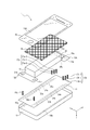
- FIG. 1 is an external perspective view illustrating a schematic configuration of a mobile wireless device according to a first embodiment of the present disclosure. It is a disassembled perspective view of the portable radio
- FIG. 2 is a cross-sectional view taken along line AA shown in FIG. It is a figure which shows a mode when signal wiring is formed also on the location in which a rib is formed. It is a disassembled perspective view of the range B shown in FIG. It is a disassembled perspective view of the other Example of the range B shown in FIG. It is a figure which shows the other example of a shape change part. It is an exploded perspective view of the structure concerning a 2nd embodiment of this indication. It is an exploded perspective view of other examples of the structure concerning a 2nd embodiment of this indication.
- An object of the present disclosure made in view of such a point is to provide a portable wireless device having a new structure that contributes to further miniaturization.
- FIG. 1 is an external perspective view showing a schematic configuration of the mobile wireless device 1 according to the first embodiment of the present disclosure.
- FIG. 2 is an exploded perspective view of the portable wireless device 1 shown in FIG.
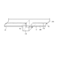
- FIG. 3 is a cross-sectional view along the line AA shown in FIG. Note that the short direction of the portable wireless device 1 is the x-axis direction, the longitudinal direction of the portable wireless device 1 is the y-axis direction, and the thickness direction of the portable wireless device 1 is the z-axis direction.
- FIG. 3 shows a part of the portable wireless device 1.
- the portable wireless device 1 is, for example, a smartphone.
- the portable wireless device 1 may be a portable device having a wireless communication function other than a smartphone.
- the mobile wireless device 1 may be a mobile phone terminal, a Fablet, a tablet PC, a feature phone, a PDA, a remote control terminal, a portable music player, a game machine, an electronic book reader, or the like.
- the portable wireless device 1 includes an external housing 10, an internal housing 11, a first substrate 12A, a second substrate 12B, a battery 13, a display device 14, a panel 15, and connection members 16a and 16b. Connecting members 17a and 17b.
- the external housing 10 is made of, for example, metal or hardened plastic.
- the external housing 10 has a rectangular shape, for example.
- the external housing 10 has an opening on the upper side thereof.
- An internal housing 11 and the like are accommodated in the external housing 10.
- a panel 15 is attached to the opening of the external housing 10.
- the outer casing 10 is formed with a fitting portion.
- the fitting portion is, for example, a concave groove 10A as shown in FIG.
- the fitting portion is fitted to a shape changing portion formed in the inner housing 11.
- the shape changing portion is, for example, a convex rib 11A as shown in FIG.
- the groove 10A is provided at a position facing the rib 11A formed in the internal housing 11, as shown in FIG.
- FIG. 2 when the rib 11A is formed on one side in the x-axis direction of the internal housing 11, the groove 10A is also formed on one side in the x-axis direction, for example, at a dotted line 10a.
- FIG. 2 when the rib 11A is formed on one side in the x-axis direction of the internal housing 11, the groove 10A is also formed on one side in the x-axis direction, for example, at a dotted line 10a.
- FIG. 2 when the rib 11A is formed on one side in the x-axis direction of
- the groove 10A is also formed on the other side of the x-axis, for example, at the dotted line 10b.
- the groove 10 ⁇ / b> A is fitted into a rib 11 ⁇ / b> A formed in the inner casing 11.
- a wiring electrically connected to the signal wiring 23a and the ground wirings 24a and 25a is formed.
- wirings that are electrically connected to the signal wirings 23 a and the like are formed in the three grooves 10 ⁇ / b> A located on the right side in FIG. 3.
- wirings electrically connected to the ground wirings 24b and 25b are formed. Details of this structure will be described later.
- the internal housing 11 is, for example, a resin housing.
- a wiring that electrically connects the wiring formed on the first substrate 12A and the wiring formed on the second substrate 12B is formed.
- a wiring 23a is formed.
- ground wirings 24 a and 25 a are formed along the signal wiring 23 a on one side of the inner housing 11 in the x-axis direction.
- the signal wiring 23e formed on the first substrate 12A and the antenna 21b as the wiring formed on the second substrate 12B are electrically connected to the other side in the x-axis direction of the inner housing 11.
- a signal wiring 23b is formed.
- ground wirings 24b and 25b are formed along the signal wiring 23b on the other side in the x-axis direction of the internal housing 11.
- the ground wirings 24a and 25a may be disposed in the vicinity of the signal wiring 23a.
- the ground wirings 24a and 25a may be arranged at positions sandwiching the signal wiring 23a, and a coplanar line (or strip line) may be formed by the signal wiring 23a and the ground wirings 24a and 25a.
- the ground wirings 24b and 25b may be disposed in the vicinity of the signal wiring 23b.
- the ground wirings 24b and 25b may be arranged at positions sandwiching the signal wiring 23b, and a coplanar line (or strip line) formed by the signal wiring 23b and the ground wirings 24b and 25b may be formed.
- LDS Laser Direct Structure
- the shape change part is formed in the inner casing 11.
- the shape changing portion is, for example, the rib 11A as shown in FIG.
- casing 11 includes the bending part which is bent intentionally in order to avoid components, such as a screw, for example besides rib 11A. Details of the shape changing portion will be described later.
- the first substrate 12A is, for example, a multilayer substrate.
- the first substrate 12A is, for example, a main substrate.
- an electronic component 22 that transmits and receives a high-frequency signal is disposed on the first substrate 12A.
- signal wirings 23c and 23e and ground wirings 24c and 25c are formed on the first substrate 12A.
- the second substrate 12B is, for example, a multilayer substrate.
- the second substrate 12B is, for example, a sub substrate.
- antennas 21a and 21b are formed on the second substrate 12B.
- the second substrate 12B is physically separated from the first substrate 12A.
- the battery 13 supplies power to a circuit (for example, the electronic component 22) in the portable wireless device 1.
- the battery 13 is disposed above the internal housing 11.
- the battery 13 is located between the first substrate 12A and the second substrate 12B.
- the display device 14 includes, for example, an LCD (Liquid Crystal Display), an organic EL (Electro Luminescence), an inorganic EL, or the like.
- the display device 14 is, for example, a touch screen display.
- the touch screen display detects the contact of a finger or a stylus pen and specifies the contact position.
- an opening 15A of the panel 15 is disposed above the display device 14. The user visually recognizes the display device 14 from the opening 15A.
- the panel 15 is made of, for example, an acrylic synthetic resin.
- the panel 15 has a rectangular shape, for example.
- the panel 15 has an opening 15 ⁇ / b> A at a position facing the display device 14.
- connection members 16a and 16b are, for example, spring connectors or the like.
- the connecting members 16a and 16b can have any shape such as a prismatic shape in addition to the cylindrical shape shown in FIG.
- the connecting member 16a electrically connects the antenna 21a formed on the second substrate 12B and the signal wiring 23a formed on the internal housing 11.
- the connection member 16b electrically connects the antenna 21b formed on the second substrate 12B and the signal wiring 23b formed on the internal housing 11.
- connection members 17a and 17b are, for example, spring connectors or the like.
- the connecting members 17a and 17b can have any shape such as a prismatic shape in addition to the cylindrical shape shown in FIG.
- the connecting member 17a includes connecting members 17a-1, 17a-2, and 17a-3.
- the connection member 17a-1 electrically connects the signal wiring 23c formed on the first substrate 12A and the signal wiring 23a formed on the internal housing 11.
- the connection member 17a-2 electrically connects the ground wiring 24c formed on the first substrate 12A and the ground wiring 24a formed on the internal housing 11.
- the connection member 17a-3 electrically connects the ground wiring 25c formed on the first substrate 12A and the ground wiring 25a formed on the internal housing 11.
- connection member 17b includes connection members 17b-1, 17b-2, and 17b-3.
- the connection member 17b-1 electrically connects the signal wiring 23e formed on the first substrate 12A and the signal wiring 23b formed on the internal housing 11.
- the connection member 17b-2 electrically connects the ground wiring 24c formed on the first substrate 12A and the ground wiring 24b formed on the internal housing 11.
- the connection member 17b-3 electrically connects the ground wiring 25c formed on the first substrate 12A and the ground wiring 25b formed on the internal housing 11.
- the electronic component 22 generates a high frequency signal.
- the high frequency signal generated by the electronic component 22 is radiated as an electromagnetic wave from the antenna 21a via the signal wiring 23c and the signal wiring 23a.
- the high-frequency signal generated by the electronic component 22 is radiated as an electromagnetic wave from the antenna 21b via the signal wiring 23e and the signal wiring 23b.
- the antenna 21a converts the received electromagnetic wave into a high-frequency signal and supplies it to the electronic component 22 via the signal wiring 23a and the signal wiring 23c.
- the antenna 21b converts the received electromagnetic wave into a high frequency signal and supplies it to the electronic component 22 via the signal wiring 23b and the signal wiring 23e.
- the electronic component 22 processes the supplied high frequency signal.
- the shape changing portion is a portion where a high frequency signal propagating through the signal wiring is reflected due to a change in impedance characteristics when the signal wiring is formed in the internal casing.
- the shape changing portion is, for example, the rib 11A as described above. This phenomenon will be described with reference to FIG.
- the signal wiring 23 ⁇ / b> X and the ground wirings 24 ⁇ / b> X and 25 ⁇ / b> X are disposed under the internal housing 11. Further, in FIG. 4, the signal wiring 23 ⁇ / b> X and the ground wirings 24 ⁇ / b> X and 25 ⁇ / b> X are continuously formed over the rib 11 ⁇ / b> A formed under the inner housing 11. In FIG. 4, the ground wirings 24X and 25X are formed as a plate-like wiring pattern, and a coplanar line is formed by the signal wiring 23X and the ground wirings 24X and 25X. In FIG.
- a high frequency signal propagating from the position P1 to the position P2 of the signal wiring 23X is reflected by a change in impedance characteristics at the position P3 where the signal wiring 23X is deformed depending on the rib 11A.
- the wiring such as the signal wires 23a and 23b formed in the internal housing 11 is bypassed so as to bypass the shape change portion.
- a relay unit for relaying is further provided.
- the relay unit according to the first embodiment is disposed at a position facing the shape changing unit of the internal housing 11.
- the relay unit according to the first embodiment will be described in detail. In the following, it is assumed that the shape changing portion is the rib 11A. In addition, the relay portion is disposed in the groove 10A facing the rib 11A.
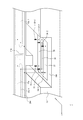
- FIG. 5 is an exploded perspective view of a range B shown in FIG.
- the signal wirings 23a-1 and 23a-2 are included in the signal wiring 23a shown in FIG.
- the ground wirings 24a-1 and 24a-2 are included in the ground wiring 24a shown in FIG.
- the ground wirings 25a-1 and 25a-2 are included in the ground wiring 25a shown in FIG.
- signal wirings 23 a-1, 23 a-2 and 24 a-1, 24 a-2, 25 a-1, 25 a-2 are formed under the internal housing 11.
- the ground wirings 24a-1 and 25a-1 are formed as a plate-like wiring pattern, and a coplanar line is formed by the signal wiring 23a-1 and the ground wirings 24a-1 and 25a-1.
- the ground wirings 24a-2 and 25a-2 are formed as a plate-like wiring pattern, and a coplanar line is formed by the signal wiring 23a-2 and the ground wirings 24a-2 and 25a-2.
- the signal wiring 23a-1 is a wiring of the internal housing 11 formed on one side of the rib 11A in the y-axis direction.
- the signal wiring 23a-2 is a wiring of the internal housing 11 formed on the other side of the rib 11A in the y-axis direction.
- the ground wiring 24a-1 is a wiring of the inner casing 11 formed on one side of the rib 11A in the y-axis direction.
- the ground wiring 24a-2 is a wiring for the internal housing 11 formed on the other side of the rib 11A in the y-axis direction.
- the ground wiring 25b-1 is a wiring of the inner casing 11 formed on one side of the rib 11A in the y-axis direction.
- the ground wiring 25b-2 is a wiring for the internal housing 11 formed on the other side of the rib 11A in the y-axis direction.
- connection members 33-1, 34-1 and 35-1 are, for example, spring connectors.
- the connecting members 33-1, 34-1 and 35-1 can have any shape such as a prismatic shape in addition to the cylindrical shape shown in FIG.
- the connection member 33-1 electrically connects the signal wiring 23a-1 and the wiring 36.
- the connection member 34-1 electrically connects the ground wiring 24a-1 and the wiring 37.
- the connection member 35-1 electrically connects the ground wiring 25a-1 and the wiring 38.
- connection members 33-2, 34-2, and 35-2 are, for example, spring connectors.
- the connection members 33-2, 34-2, and 35-2 can have an arbitrary shape such as a prismatic shape in addition to the cylindrical shape shown in FIG.
- the connection member 33-2 electrically connects the signal wiring 23a-2 and the wiring 36.
- the connection member 34-2 electrically connects the ground wiring 24a-2 and the wiring 37.
- the connection member 35-2 electrically connects the ground wiring 25a-2 and the wiring 38.
- the wirings 36, 37, and 38 are formed on the bottom of the concave groove 10A.
- the wirings 37 and 38 are formed as a plate-like wiring pattern, and a coplanar line is formed by the wiring 36 and the wirings 37 and 38.
- One end of the wiring 36 in the y-axis direction is electrically connected to the connection member 33-1.
- the other end of the wiring 36 in the y-axis direction is electrically connected to the connection member 33-2.
- One end of the wiring 37 in the y-axis direction is electrically connected to the connecting member 34-1.
- the other end of the wiring 37 in the y-axis direction is electrically connected to the connection member 34-2.
- One end of the wiring 38 in the y-axis direction is electrically connected to the connection member 35-1.
- the other end of the wiring 38 in the y-axis direction is electrically connected to the connection member 35-2.
- connection members 33-1 and 33-2 and the wirings 36 as relay portions are arranged on the bottom of the concave groove 10A facing the rib 11A. Further, the connection members 33-1 and 33-2 and the wiring 36 as the relay portion are connected to the signal wiring 23a-1 formed in the inner casing 11 and the signal wiring 23a-2 formed in the inner casing 11. Connect electrically.
- connection members 34-1 and 34-2 as the relay portions and the wiring 37 are arranged on the bottom of the concave groove 10A facing the rib 11A. Further, the connection members 34-1 and 34-2 and the wiring 37 as the relay portion are connected to the ground wiring 24a-1 formed in the inner casing 11 and the ground wiring 24a-2 formed in the inner casing 11. Connect electrically.
- connection members 35-1 and 35-2 as the relay portions and the wiring 38 are disposed on the bottom of the concave groove 10A facing the rib 11A. Further, the connection members 35-1 and 35-2 and the wiring 38 as the relay portion are connected to the ground wiring 25a-1 formed in the internal casing 11 and the ground wiring 25a-2 formed in the internal casing 11. Connect electrically.
- the signal wiring 23b and the ground wirings 24b and 25b shown in FIG. 2 are relayed by the relay unit as shown in FIG. 5 so as to bypass the rib 11A, similarly to the signal wiring 23a and the ground wirings 24a and 25a.
- the signal wiring 23c and the like formed on the first substrate 12A and the antenna 21a and the like formed on the second substrate 12B are electrically connected.
- a signal wiring 23 a and the like are formed in the internal housing 11. That is, the high-frequency signal from the first substrate 12A is not transmitted to the antennas 21a and 21b by the coaxial cable, but is transmitted by the signal wirings 23a and 23b formed in the internal casing 11. Therefore, the portable wireless device 1 does not have to provide a region for arranging the coaxial cable.
- the portable wireless device 1 can be further downsized by such a structure that contributes to downsizing.
- the relay unit is provided by arranging the connection members 33-1 and 33-2, the wiring 36, and the like in the external housing 10. That is, no special parts or the like are used in providing the relay unit. Therefore, in the mobile wireless device 1 according to the first embodiment, a relay unit can be provided at low cost.
- the portable wireless device 1 includes a relay unit that relays the wiring formed in the internal housing 11 so as to bypass the shape changing unit such as the rib 11A.
- a relay unit that relays the wiring formed in the internal housing 11 so as to bypass the shape changing unit such as the rib 11A.
- the wiring formed in the internal housing 11 may be relayed together by one relay unit.
- a convex rib as a fitting portion may be formed in the outer casing 10, and a concave groove that fits into the rib of the outer casing 10 may be formed in the inner casing 11.
- a relay unit that relays the wiring formed in the internal housing 11 may be arranged so as to bypass the groove as the shape changing unit formed in the internal housing 11.
- the ground wirings 24a and 25a formed in the inner housing 11 may be continuously formed over the rib 11A as shown in FIG.
- the ground wiring 24a is continuously formed over the rib 11A in this way, for example, even if the potential of the wiring 37 floats, the potential of the ground wiring 24a on the signal wiring 23a-1 side and the ground on the signal wiring 23a-2 side
- the potential of the wiring 24a can be made the same.
- the ground wiring 24a and the ground wiring 25a may be integrally formed over the rib 11A as shown in FIG. When the ground wiring 24a and the like are formed in this way, it is possible to save the trouble of masking the rib 11A in the wiring formation process in order to divide the ground wiring 24a and the like into the ground wirings 24a-1 and 24a-2.
- casing 11 has is not limited to the rib 11A.
- FIG. 7 shows an inner housing 11a having a bent portion 11B.
- the bent portion 11B is intentionally formed in order to avoid parts such as screws.
- the bent portion 11B can also be a factor that causes reflection of a high-frequency signal by changing impedance characteristics. Therefore, the bent portion 11B is included in the shape changing portion. Therefore, in this case, a relay unit that relays the wiring formed in the internal housing 11a may be disposed in the external housing 10 so as to bypass the bent portion 11B.
- an arc-shaped relay unit having a desired impedance characteristic may be arranged in the external housing 10.
- the relay unit may be disposed in a portion of the external housing 10 that faces the bent portion 11B.
- the relay unit is arranged in the external housing 10 (for example, on the bottom of the groove 10A). In the second embodiment, the relay unit is arranged on the substrate.
- FIG. 8 is an exploded perspective view of the structure according to the second embodiment of the present disclosure.
- the same component as the component shown in FIG. 8 the same component as the component shown in FIG.
- the wirings 36, 37, and 38 are formed on the third substrate 39.
- One end of the wiring 36 in the y-axis direction is electrically connected to the connection member 33-1.
- the other end of the wiring 36 in the y-axis direction is electrically connected to the connection member 33-2.
- One end of the wiring 37 in the y-axis direction is electrically connected to the connection member 34-1.
- the other end of the wiring 37 in the y-axis direction is electrically connected to the connection member 34-2.
- One end of the wiring 38 in the y-axis direction is electrically connected to the connection member 35-1.
- the other end of the wiring 38 in the y-axis direction is electrically connected to the connection member 35-2.
- the third substrate 39 is disposed between the rib 11A as the shape changing portion and the external housing 10.
- the third substrate 39 is disposed between the rib 11A and the groove 10A facing the rib 11A.
- connection members 33-1 and 33-2 and the wirings 36 as relay portions are arranged on the third substrate 39.
- connection members 34-1 and 34-2 and wirings 37 as relay portions are arranged on the third substrate 39.
- connection members 35-1 and 35-2 and the wirings 38 as relay portions are arranged on the third substrate 39.
- a matching circuit that matches the impedance on the connection member 33-1 side and the impedance on the connection member 33-2 side may be disposed on the third substrate 39. By arranging the matching circuit, it is possible to reduce the transmission loss of the high-frequency signal propagating through the signal wiring 23a.
- the ground lines 24a and 25a may be continuously formed over the rib 11A as shown in FIG. Furthermore, the ground wiring 24a and the ground wiring 25a may be integrally formed over the rib 11A as shown in FIG. With such a configuration, the effects described above with reference to FIG. 6 can be obtained.
- Computer systems and other hardware include, for example, general-purpose computers, personal computers (PCs), dedicated computers, workstations, PCS (personal communications systems), electronic notepads, laptop computers or other programmable Data processing devices are included.
- the various operations are performed by dedicated circuitry implemented with program instructions (software) (e.g., individual logic gates interconnected to perform specific functions) or by one or more processors. Note that it is executed by a logical block or a program module to be executed.
- processors that execute logic blocks or program modules include, for example, one or more microprocessors, CPU (Central Processing Unit), ASIC (Application Specific Integrated Circuit), DSP (Digital Signal Processor), PLD ( Programmable Logic (Device), FPGA (Field Programmable Gate Array), controller, microcontroller, electronic device, other devices designed to perform the functions described herein, and / or any combination thereof.
- microprocessors CPU (Central Processing Unit), ASIC (Application Specific Integrated Circuit), DSP (Digital Signal Processor), PLD ( Programmable Logic (Device), FPGA (Field Programmable Gate Array), controller, microcontroller, electronic device, other devices designed to perform the functions described herein, and / or any combination thereof.
- CPU Central Processing Unit
- ASIC Application Specific Integrated Circuit
- DSP Digital Signal Processor
- PLD Programmable Logic
- FPGA Field Programmable Gate Array
- controller microcontroller
- electronic device other devices designed to perform the functions described herein, and / or any combination thereof.
- the machine-readable non-transitory storage medium used here can be further configured as a computer-readable tangible carrier (medium) composed of solid state memory, magnetic disk and optical disk.
- a medium stores an appropriate set of computer instructions and a data structure such as a program module for causing a processor to execute the technology disclosed herein.
- Computer readable media include electrical connections with one or more wires, magnetic disk storage media, other magnetic and optical storage devices (eg, CD (Compact Disk), DVD (Digital Versatile Disk), and Blu-ray disc, portable computer disk, RAM (Random Access Memory), ROM (Read-Only Memory), EPROM (Erasable Programmable Read-Only Memory), EEPROM (Electrically Erasable Programmable Read-Only Memory) or flash memory can be rewritten And / or other tangible storage media capable of storing information, or any combination thereof, which may be provided within and / or external to the processor / processing unit.
- the word “memory” is used for all kinds of long-term memory, short-term memory It means memory, volatile, non-volatile, or other memory, and the specific type or number of memories or the type of medium on which the storage is stored is not limited.
Landscapes
- Engineering & Computer Science (AREA)
- Signal Processing (AREA)
- Computer Networks & Wireless Communication (AREA)
- Telephone Set Structure (AREA)
- Transceivers (AREA)
- Waveguide Connection Structure (AREA)
- Waveguides (AREA)
Abstract
Cette invention concerne un appareil sans fil portable présentant une structure nouvelle contribuant à faciliter la miniaturisation. Cet appareil sans fil portable comprend : un premier substrat ; un second substrat qui est physiquement séparé du premier substrat ; un boîtier interne ; et une partie relais. Un câblage est formé, dans le boîtier interne, de façon à connecter électriquement un câblage formé dans le premier substrat et un câblage formé dans le second substrat. En outre, le boîtier interne comprend une partie de changement de forme. La partie relais relaie le câblage formé dans le boîtier interne de façon à contourner la partie de changement de forme
Applications Claiming Priority (2)
| Application Number | Priority Date | Filing Date | Title |
|---|---|---|---|
| JP2016-252028 | 2016-12-26 | ||
| JP2016252028A JP6643222B2 (ja) | 2016-12-26 | 2016-12-26 | 携帯無線装置 |
Publications (1)
| Publication Number | Publication Date |
|---|---|
| WO2018123736A1 true WO2018123736A1 (fr) | 2018-07-05 |
Family
ID=62708002
Family Applications (1)
| Application Number | Title | Priority Date | Filing Date |
|---|---|---|---|
| PCT/JP2017/045549 Ceased WO2018123736A1 (fr) | 2016-12-26 | 2017-12-19 | Appareil sans fil portable |
Country Status (2)
| Country | Link |
|---|---|
| JP (1) | JP6643222B2 (fr) |
| WO (1) | WO2018123736A1 (fr) |
Citations (3)
| Publication number | Priority date | Publication date | Assignee | Title |
|---|---|---|---|---|
| JPH10173410A (ja) * | 1996-12-12 | 1998-06-26 | Sharp Corp | ストリップ線路を用いた伝送回路 |
| US20060097388A1 (en) * | 2002-07-02 | 2006-05-11 | Klaus Breitschwerdt | Electrical system, especially a microelectronic or microelectromechanical high frequency system |
| JP2010283539A (ja) * | 2009-06-03 | 2010-12-16 | Sony Ericsson Mobilecommunications Japan Inc | 携帯型無線通信装置 |
-
2016
- 2016-12-26 JP JP2016252028A patent/JP6643222B2/ja active Active
-
2017
- 2017-12-19 WO PCT/JP2017/045549 patent/WO2018123736A1/fr not_active Ceased
Patent Citations (3)
| Publication number | Priority date | Publication date | Assignee | Title |
|---|---|---|---|---|
| JPH10173410A (ja) * | 1996-12-12 | 1998-06-26 | Sharp Corp | ストリップ線路を用いた伝送回路 |
| US20060097388A1 (en) * | 2002-07-02 | 2006-05-11 | Klaus Breitschwerdt | Electrical system, especially a microelectronic or microelectromechanical high frequency system |
| JP2010283539A (ja) * | 2009-06-03 | 2010-12-16 | Sony Ericsson Mobilecommunications Japan Inc | 携帯型無線通信装置 |
Also Published As
| Publication number | Publication date |
|---|---|
| JP2018107631A (ja) | 2018-07-05 |
| JP6643222B2 (ja) | 2020-02-12 |
Similar Documents
| Publication | Publication Date | Title |
|---|---|---|
| US11637578B2 (en) | Antenna and foldable electronic device including the same | |
| US9462094B2 (en) | Device housing and portable electronic device using same | |
| EP3338322B1 (fr) | Dispositif électronique | |
| US9645608B1 (en) | Portable electronic device | |
| US10103435B2 (en) | Systems and methods for transloop impedance matching of an antenna | |
| US10547108B2 (en) | Antenna device and electronic device including the same | |
| KR102769071B1 (ko) | 안테나를 포함하는 전자 장치 | |
| KR102919981B1 (ko) | 안테나 패턴을 포함하는 플렉서블 어셈블리 및 이를 포함하는 전자 장치 | |
| US8753151B2 (en) | Connector module and handheld electronic device | |
| AU2016101259A4 (en) | Antennas for electronic device with heat spreader | |
| KR20200048238A (ko) | 벤딩 특성을 갖는 배선 부재 및 이를 포함하는 전자 장치 | |
| US12261358B2 (en) | Antenna device | |
| JPWO2017073020A1 (ja) | 電子機器 | |
| CN109950701A (zh) | 天线组件和移动终端 | |
| US9927846B2 (en) | Flash drive structure | |
| US10810480B2 (en) | Electronic tag and electronic system using the same | |
| KR102922120B1 (ko) | 노이즈 필터 구조를 포함하는 인쇄 회로 기판 및 이를 포함하는 전자 장치 | |
| TWI736232B (zh) | 電子裝置 | |
| WO2018123736A1 (fr) | Appareil sans fil portable | |
| KR102857207B1 (ko) | 안테나 구조 및 이를 포함하는 전자 장치 | |
| WO2018123566A1 (fr) | Dispositif sans fil portable | |
| US20170086323A1 (en) | Electronic device and component module | |
| US8896491B1 (en) | Cross-type transmission module | |
| KR20250047555A (ko) | 안테나의 그라운드를 위한 연결 구조를 포함하는 전자 장치 | |
| KR20240158835A (ko) | 카메라 어셈블리 및 전자 장치 |
Legal Events
| Date | Code | Title | Description |
|---|---|---|---|
| 121 | Ep: the epo has been informed by wipo that ep was designated in this application |
Ref document number: 17889357 Country of ref document: EP Kind code of ref document: A1 |
|
| NENP | Non-entry into the national phase |
Ref country code: DE |
|
| 122 | Ep: pct application non-entry in european phase |
Ref document number: 17889357 Country of ref document: EP Kind code of ref document: A1 |