WO2018123736A1 - 携帯無線装置 - Google Patents
携帯無線装置 Download PDFInfo
- Publication number
- WO2018123736A1 WO2018123736A1 PCT/JP2017/045549 JP2017045549W WO2018123736A1 WO 2018123736 A1 WO2018123736 A1 WO 2018123736A1 JP 2017045549 W JP2017045549 W JP 2017045549W WO 2018123736 A1 WO2018123736 A1 WO 2018123736A1
- Authority
- WO
- WIPO (PCT)
- Prior art keywords
- wiring
- substrate
- wireless device
- portable wireless
- ground
- Prior art date
- Legal status (The legal status is an assumption and is not a legal conclusion. Google has not performed a legal analysis and makes no representation as to the accuracy of the status listed.)
- Ceased
Links
Images


Classifications
-
- H—ELECTRICITY
- H01—ELECTRIC ELEMENTS
- H01P—WAVEGUIDES; RESONATORS, LINES, OR OTHER DEVICES OF THE WAVEGUIDE TYPE
- H01P1/00—Auxiliary devices
- H01P1/04—Fixed joints
-
- H—ELECTRICITY
- H01—ELECTRIC ELEMENTS
- H01P—WAVEGUIDES; RESONATORS, LINES, OR OTHER DEVICES OF THE WAVEGUIDE TYPE
- H01P3/00—Waveguides; Transmission lines of the waveguide type
-
- H—ELECTRICITY
- H01—ELECTRIC ELEMENTS
- H01P—WAVEGUIDES; RESONATORS, LINES, OR OTHER DEVICES OF THE WAVEGUIDE TYPE
- H01P3/00—Waveguides; Transmission lines of the waveguide type
- H01P3/02—Waveguides; Transmission lines of the waveguide type with two longitudinal conductors
- H01P3/08—Microstrips; Strip lines
-
- H—ELECTRICITY
- H04—ELECTRIC COMMUNICATION TECHNIQUE
- H04B—TRANSMISSION
- H04B1/00—Details of transmission systems, not covered by a single one of groups H04B3/00 - H04B13/00; Details of transmission systems not characterised by the medium used for transmission
- H04B1/38—Transceivers, i.e. devices in which transmitter and receiver form a structural unit and in which at least one part is used for functions of transmitting and receiving
- H04B1/3827—Portable transceivers
-
- H—ELECTRICITY
- H04—ELECTRIC COMMUNICATION TECHNIQUE
- H04M—TELEPHONIC COMMUNICATION
- H04M1/00—Substation equipment, e.g. for use by subscribers
- H04M1/02—Constructional features of telephone sets
Definitions
- the present disclosure relates to a portable wireless device.
- Patent Document 1 discloses a portable wireless device that employs a structure that transmits a high-frequency signal from a main circuit board to an antenna board via a coaxial cable.
- a portable wireless device includes a first substrate, a second substrate physically separated from the first substrate, an internal housing, and a relay unit.
- a wiring for electrically connecting a wiring formed on the first substrate and a wiring formed on the second substrate is formed in the internal housing.
- the internal housing has a shape changing portion.
- the relay unit relays the wiring formed in the internal casing so as to bypass the shape changing unit.
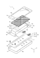
- FIG. 1 is an external perspective view illustrating a schematic configuration of a mobile wireless device according to a first embodiment of the present disclosure. It is a disassembled perspective view of the portable radio
- FIG. 2 is a cross-sectional view taken along line AA shown in FIG. It is a figure which shows a mode when signal wiring is formed also on the location in which a rib is formed. It is a disassembled perspective view of the range B shown in FIG. It is a disassembled perspective view of the other Example of the range B shown in FIG. It is a figure which shows the other example of a shape change part. It is an exploded perspective view of the structure concerning a 2nd embodiment of this indication. It is an exploded perspective view of other examples of the structure concerning a 2nd embodiment of this indication.
- An object of the present disclosure made in view of such a point is to provide a portable wireless device having a new structure that contributes to further miniaturization.
- FIG. 1 is an external perspective view showing a schematic configuration of the mobile wireless device 1 according to the first embodiment of the present disclosure.
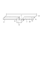
- FIG. 2 is an exploded perspective view of the portable wireless device 1 shown in FIG.
- FIG. 3 is a cross-sectional view along the line AA shown in FIG. Note that the short direction of the portable wireless device 1 is the x-axis direction, the longitudinal direction of the portable wireless device 1 is the y-axis direction, and the thickness direction of the portable wireless device 1 is the z-axis direction.
- FIG. 3 shows a part of the portable wireless device 1.
- the portable wireless device 1 is, for example, a smartphone.
- the portable wireless device 1 may be a portable device having a wireless communication function other than a smartphone.
- the mobile wireless device 1 may be a mobile phone terminal, a Fablet, a tablet PC, a feature phone, a PDA, a remote control terminal, a portable music player, a game machine, an electronic book reader, or the like.
- the portable wireless device 1 includes an external housing 10, an internal housing 11, a first substrate 12A, a second substrate 12B, a battery 13, a display device 14, a panel 15, and connection members 16a and 16b. Connecting members 17a and 17b.
- the external housing 10 is made of, for example, metal or hardened plastic.
- the external housing 10 has a rectangular shape, for example.
- the external housing 10 has an opening on the upper side thereof.
- An internal housing 11 and the like are accommodated in the external housing 10.
- a panel 15 is attached to the opening of the external housing 10.
- the outer casing 10 is formed with a fitting portion.
- the fitting portion is, for example, a concave groove 10A as shown in FIG.
- the fitting portion is fitted to a shape changing portion formed in the inner housing 11.
- the shape changing portion is, for example, a convex rib 11A as shown in FIG.
- the groove 10A is provided at a position facing the rib 11A formed in the internal housing 11, as shown in FIG.
- FIG. 2 when the rib 11A is formed on one side in the x-axis direction of the internal housing 11, the groove 10A is also formed on one side in the x-axis direction, for example, at a dotted line 10a.
- FIG. 2 when the rib 11A is formed on one side in the x-axis direction of the internal housing 11, the groove 10A is also formed on one side in the x-axis direction, for example, at a dotted line 10a.
- FIG. 2 when the rib 11A is formed on one side in the x-axis direction of
- the groove 10A is also formed on the other side of the x-axis, for example, at the dotted line 10b.
- the groove 10 ⁇ / b> A is fitted into a rib 11 ⁇ / b> A formed in the inner casing 11.
- a wiring electrically connected to the signal wiring 23a and the ground wirings 24a and 25a is formed.
- wirings that are electrically connected to the signal wirings 23 a and the like are formed in the three grooves 10 ⁇ / b> A located on the right side in FIG. 3.
- wirings electrically connected to the ground wirings 24b and 25b are formed. Details of this structure will be described later.
- the internal housing 11 is, for example, a resin housing.
- a wiring that electrically connects the wiring formed on the first substrate 12A and the wiring formed on the second substrate 12B is formed.
- a wiring 23a is formed.
- ground wirings 24 a and 25 a are formed along the signal wiring 23 a on one side of the inner housing 11 in the x-axis direction.
- the signal wiring 23e formed on the first substrate 12A and the antenna 21b as the wiring formed on the second substrate 12B are electrically connected to the other side in the x-axis direction of the inner housing 11.
- a signal wiring 23b is formed.
- ground wirings 24b and 25b are formed along the signal wiring 23b on the other side in the x-axis direction of the internal housing 11.
- the ground wirings 24a and 25a may be disposed in the vicinity of the signal wiring 23a.
- the ground wirings 24a and 25a may be arranged at positions sandwiching the signal wiring 23a, and a coplanar line (or strip line) may be formed by the signal wiring 23a and the ground wirings 24a and 25a.
- the ground wirings 24b and 25b may be disposed in the vicinity of the signal wiring 23b.
- the ground wirings 24b and 25b may be arranged at positions sandwiching the signal wiring 23b, and a coplanar line (or strip line) formed by the signal wiring 23b and the ground wirings 24b and 25b may be formed.
- LDS Laser Direct Structure
- the shape change part is formed in the inner casing 11.
- the shape changing portion is, for example, the rib 11A as shown in FIG.
- casing 11 includes the bending part which is bent intentionally in order to avoid components, such as a screw, for example besides rib 11A. Details of the shape changing portion will be described later.
- the first substrate 12A is, for example, a multilayer substrate.
- the first substrate 12A is, for example, a main substrate.
- an electronic component 22 that transmits and receives a high-frequency signal is disposed on the first substrate 12A.
- signal wirings 23c and 23e and ground wirings 24c and 25c are formed on the first substrate 12A.
- the second substrate 12B is, for example, a multilayer substrate.
- the second substrate 12B is, for example, a sub substrate.
- antennas 21a and 21b are formed on the second substrate 12B.
- the second substrate 12B is physically separated from the first substrate 12A.
- the battery 13 supplies power to a circuit (for example, the electronic component 22) in the portable wireless device 1.
- the battery 13 is disposed above the internal housing 11.
- the battery 13 is located between the first substrate 12A and the second substrate 12B.
- the display device 14 includes, for example, an LCD (Liquid Crystal Display), an organic EL (Electro Luminescence), an inorganic EL, or the like.
- the display device 14 is, for example, a touch screen display.
- the touch screen display detects the contact of a finger or a stylus pen and specifies the contact position.
- an opening 15A of the panel 15 is disposed above the display device 14. The user visually recognizes the display device 14 from the opening 15A.
- the panel 15 is made of, for example, an acrylic synthetic resin.
- the panel 15 has a rectangular shape, for example.
- the panel 15 has an opening 15 ⁇ / b> A at a position facing the display device 14.
- connection members 16a and 16b are, for example, spring connectors or the like.
- the connecting members 16a and 16b can have any shape such as a prismatic shape in addition to the cylindrical shape shown in FIG.
- the connecting member 16a electrically connects the antenna 21a formed on the second substrate 12B and the signal wiring 23a formed on the internal housing 11.
- the connection member 16b electrically connects the antenna 21b formed on the second substrate 12B and the signal wiring 23b formed on the internal housing 11.
- connection members 17a and 17b are, for example, spring connectors or the like.
- the connecting members 17a and 17b can have any shape such as a prismatic shape in addition to the cylindrical shape shown in FIG.
- the connecting member 17a includes connecting members 17a-1, 17a-2, and 17a-3.
- the connection member 17a-1 electrically connects the signal wiring 23c formed on the first substrate 12A and the signal wiring 23a formed on the internal housing 11.
- the connection member 17a-2 electrically connects the ground wiring 24c formed on the first substrate 12A and the ground wiring 24a formed on the internal housing 11.
- the connection member 17a-3 electrically connects the ground wiring 25c formed on the first substrate 12A and the ground wiring 25a formed on the internal housing 11.
- connection member 17b includes connection members 17b-1, 17b-2, and 17b-3.
- the connection member 17b-1 electrically connects the signal wiring 23e formed on the first substrate 12A and the signal wiring 23b formed on the internal housing 11.
- the connection member 17b-2 electrically connects the ground wiring 24c formed on the first substrate 12A and the ground wiring 24b formed on the internal housing 11.
- the connection member 17b-3 electrically connects the ground wiring 25c formed on the first substrate 12A and the ground wiring 25b formed on the internal housing 11.
- the electronic component 22 generates a high frequency signal.
- the high frequency signal generated by the electronic component 22 is radiated as an electromagnetic wave from the antenna 21a via the signal wiring 23c and the signal wiring 23a.
- the high-frequency signal generated by the electronic component 22 is radiated as an electromagnetic wave from the antenna 21b via the signal wiring 23e and the signal wiring 23b.
- the antenna 21a converts the received electromagnetic wave into a high-frequency signal and supplies it to the electronic component 22 via the signal wiring 23a and the signal wiring 23c.
- the antenna 21b converts the received electromagnetic wave into a high frequency signal and supplies it to the electronic component 22 via the signal wiring 23b and the signal wiring 23e.
- the electronic component 22 processes the supplied high frequency signal.
- the shape changing portion is a portion where a high frequency signal propagating through the signal wiring is reflected due to a change in impedance characteristics when the signal wiring is formed in the internal casing.
- the shape changing portion is, for example, the rib 11A as described above. This phenomenon will be described with reference to FIG.
- the signal wiring 23 ⁇ / b> X and the ground wirings 24 ⁇ / b> X and 25 ⁇ / b> X are disposed under the internal housing 11. Further, in FIG. 4, the signal wiring 23 ⁇ / b> X and the ground wirings 24 ⁇ / b> X and 25 ⁇ / b> X are continuously formed over the rib 11 ⁇ / b> A formed under the inner housing 11. In FIG. 4, the ground wirings 24X and 25X are formed as a plate-like wiring pattern, and a coplanar line is formed by the signal wiring 23X and the ground wirings 24X and 25X. In FIG.
- a high frequency signal propagating from the position P1 to the position P2 of the signal wiring 23X is reflected by a change in impedance characteristics at the position P3 where the signal wiring 23X is deformed depending on the rib 11A.
- the wiring such as the signal wires 23a and 23b formed in the internal housing 11 is bypassed so as to bypass the shape change portion.
- a relay unit for relaying is further provided.
- the relay unit according to the first embodiment is disposed at a position facing the shape changing unit of the internal housing 11.
- the relay unit according to the first embodiment will be described in detail. In the following, it is assumed that the shape changing portion is the rib 11A. In addition, the relay portion is disposed in the groove 10A facing the rib 11A.
- FIG. 5 is an exploded perspective view of a range B shown in FIG.
- the signal wirings 23a-1 and 23a-2 are included in the signal wiring 23a shown in FIG.
- the ground wirings 24a-1 and 24a-2 are included in the ground wiring 24a shown in FIG.
- the ground wirings 25a-1 and 25a-2 are included in the ground wiring 25a shown in FIG.
- signal wirings 23 a-1, 23 a-2 and 24 a-1, 24 a-2, 25 a-1, 25 a-2 are formed under the internal housing 11.
- the ground wirings 24a-1 and 25a-1 are formed as a plate-like wiring pattern, and a coplanar line is formed by the signal wiring 23a-1 and the ground wirings 24a-1 and 25a-1.
- the ground wirings 24a-2 and 25a-2 are formed as a plate-like wiring pattern, and a coplanar line is formed by the signal wiring 23a-2 and the ground wirings 24a-2 and 25a-2.
- the signal wiring 23a-1 is a wiring of the internal housing 11 formed on one side of the rib 11A in the y-axis direction.
- the signal wiring 23a-2 is a wiring of the internal housing 11 formed on the other side of the rib 11A in the y-axis direction.
- the ground wiring 24a-1 is a wiring of the inner casing 11 formed on one side of the rib 11A in the y-axis direction.
- the ground wiring 24a-2 is a wiring for the internal housing 11 formed on the other side of the rib 11A in the y-axis direction.
- the ground wiring 25b-1 is a wiring of the inner casing 11 formed on one side of the rib 11A in the y-axis direction.
- the ground wiring 25b-2 is a wiring for the internal housing 11 formed on the other side of the rib 11A in the y-axis direction.
- connection members 33-1, 34-1 and 35-1 are, for example, spring connectors.
- the connecting members 33-1, 34-1 and 35-1 can have any shape such as a prismatic shape in addition to the cylindrical shape shown in FIG.
- the connection member 33-1 electrically connects the signal wiring 23a-1 and the wiring 36.
- the connection member 34-1 electrically connects the ground wiring 24a-1 and the wiring 37.
- the connection member 35-1 electrically connects the ground wiring 25a-1 and the wiring 38.
- connection members 33-2, 34-2, and 35-2 are, for example, spring connectors.
- the connection members 33-2, 34-2, and 35-2 can have an arbitrary shape such as a prismatic shape in addition to the cylindrical shape shown in FIG.
- the connection member 33-2 electrically connects the signal wiring 23a-2 and the wiring 36.
- the connection member 34-2 electrically connects the ground wiring 24a-2 and the wiring 37.
- the connection member 35-2 electrically connects the ground wiring 25a-2 and the wiring 38.
- the wirings 36, 37, and 38 are formed on the bottom of the concave groove 10A.
- the wirings 37 and 38 are formed as a plate-like wiring pattern, and a coplanar line is formed by the wiring 36 and the wirings 37 and 38.
- One end of the wiring 36 in the y-axis direction is electrically connected to the connection member 33-1.
- the other end of the wiring 36 in the y-axis direction is electrically connected to the connection member 33-2.
- One end of the wiring 37 in the y-axis direction is electrically connected to the connecting member 34-1.
- the other end of the wiring 37 in the y-axis direction is electrically connected to the connection member 34-2.
- One end of the wiring 38 in the y-axis direction is electrically connected to the connection member 35-1.
- the other end of the wiring 38 in the y-axis direction is electrically connected to the connection member 35-2.
- connection members 33-1 and 33-2 and the wirings 36 as relay portions are arranged on the bottom of the concave groove 10A facing the rib 11A. Further, the connection members 33-1 and 33-2 and the wiring 36 as the relay portion are connected to the signal wiring 23a-1 formed in the inner casing 11 and the signal wiring 23a-2 formed in the inner casing 11. Connect electrically.
- connection members 34-1 and 34-2 as the relay portions and the wiring 37 are arranged on the bottom of the concave groove 10A facing the rib 11A. Further, the connection members 34-1 and 34-2 and the wiring 37 as the relay portion are connected to the ground wiring 24a-1 formed in the inner casing 11 and the ground wiring 24a-2 formed in the inner casing 11. Connect electrically.
- connection members 35-1 and 35-2 as the relay portions and the wiring 38 are disposed on the bottom of the concave groove 10A facing the rib 11A. Further, the connection members 35-1 and 35-2 and the wiring 38 as the relay portion are connected to the ground wiring 25a-1 formed in the internal casing 11 and the ground wiring 25a-2 formed in the internal casing 11. Connect electrically.
- the signal wiring 23b and the ground wirings 24b and 25b shown in FIG. 2 are relayed by the relay unit as shown in FIG. 5 so as to bypass the rib 11A, similarly to the signal wiring 23a and the ground wirings 24a and 25a.
- the signal wiring 23c and the like formed on the first substrate 12A and the antenna 21a and the like formed on the second substrate 12B are electrically connected.
- a signal wiring 23 a and the like are formed in the internal housing 11. That is, the high-frequency signal from the first substrate 12A is not transmitted to the antennas 21a and 21b by the coaxial cable, but is transmitted by the signal wirings 23a and 23b formed in the internal casing 11. Therefore, the portable wireless device 1 does not have to provide a region for arranging the coaxial cable.
- the portable wireless device 1 can be further downsized by such a structure that contributes to downsizing.
- the relay unit is provided by arranging the connection members 33-1 and 33-2, the wiring 36, and the like in the external housing 10. That is, no special parts or the like are used in providing the relay unit. Therefore, in the mobile wireless device 1 according to the first embodiment, a relay unit can be provided at low cost.
- the portable wireless device 1 includes a relay unit that relays the wiring formed in the internal housing 11 so as to bypass the shape changing unit such as the rib 11A.
- a relay unit that relays the wiring formed in the internal housing 11 so as to bypass the shape changing unit such as the rib 11A.
- the wiring formed in the internal housing 11 may be relayed together by one relay unit.
- a convex rib as a fitting portion may be formed in the outer casing 10, and a concave groove that fits into the rib of the outer casing 10 may be formed in the inner casing 11.
- a relay unit that relays the wiring formed in the internal housing 11 may be arranged so as to bypass the groove as the shape changing unit formed in the internal housing 11.
- the ground wirings 24a and 25a formed in the inner housing 11 may be continuously formed over the rib 11A as shown in FIG.
- the ground wiring 24a is continuously formed over the rib 11A in this way, for example, even if the potential of the wiring 37 floats, the potential of the ground wiring 24a on the signal wiring 23a-1 side and the ground on the signal wiring 23a-2 side
- the potential of the wiring 24a can be made the same.
- the ground wiring 24a and the ground wiring 25a may be integrally formed over the rib 11A as shown in FIG. When the ground wiring 24a and the like are formed in this way, it is possible to save the trouble of masking the rib 11A in the wiring formation process in order to divide the ground wiring 24a and the like into the ground wirings 24a-1 and 24a-2.
- casing 11 has is not limited to the rib 11A.
- FIG. 7 shows an inner housing 11a having a bent portion 11B.
- the bent portion 11B is intentionally formed in order to avoid parts such as screws.
- the bent portion 11B can also be a factor that causes reflection of a high-frequency signal by changing impedance characteristics. Therefore, the bent portion 11B is included in the shape changing portion. Therefore, in this case, a relay unit that relays the wiring formed in the internal housing 11a may be disposed in the external housing 10 so as to bypass the bent portion 11B.
- an arc-shaped relay unit having a desired impedance characteristic may be arranged in the external housing 10.
- the relay unit may be disposed in a portion of the external housing 10 that faces the bent portion 11B.
- the relay unit is arranged in the external housing 10 (for example, on the bottom of the groove 10A). In the second embodiment, the relay unit is arranged on the substrate.
- FIG. 8 is an exploded perspective view of the structure according to the second embodiment of the present disclosure.
- the same component as the component shown in FIG. 8 the same component as the component shown in FIG.
- the wirings 36, 37, and 38 are formed on the third substrate 39.
- One end of the wiring 36 in the y-axis direction is electrically connected to the connection member 33-1.
- the other end of the wiring 36 in the y-axis direction is electrically connected to the connection member 33-2.
- One end of the wiring 37 in the y-axis direction is electrically connected to the connection member 34-1.
- the other end of the wiring 37 in the y-axis direction is electrically connected to the connection member 34-2.
- One end of the wiring 38 in the y-axis direction is electrically connected to the connection member 35-1.
- the other end of the wiring 38 in the y-axis direction is electrically connected to the connection member 35-2.
- the third substrate 39 is disposed between the rib 11A as the shape changing portion and the external housing 10.
- the third substrate 39 is disposed between the rib 11A and the groove 10A facing the rib 11A.
- connection members 33-1 and 33-2 and the wirings 36 as relay portions are arranged on the third substrate 39.
- connection members 34-1 and 34-2 and wirings 37 as relay portions are arranged on the third substrate 39.
- connection members 35-1 and 35-2 and the wirings 38 as relay portions are arranged on the third substrate 39.
- a matching circuit that matches the impedance on the connection member 33-1 side and the impedance on the connection member 33-2 side may be disposed on the third substrate 39. By arranging the matching circuit, it is possible to reduce the transmission loss of the high-frequency signal propagating through the signal wiring 23a.
- the ground lines 24a and 25a may be continuously formed over the rib 11A as shown in FIG. Furthermore, the ground wiring 24a and the ground wiring 25a may be integrally formed over the rib 11A as shown in FIG. With such a configuration, the effects described above with reference to FIG. 6 can be obtained.
- Computer systems and other hardware include, for example, general-purpose computers, personal computers (PCs), dedicated computers, workstations, PCS (personal communications systems), electronic notepads, laptop computers or other programmable Data processing devices are included.
- the various operations are performed by dedicated circuitry implemented with program instructions (software) (e.g., individual logic gates interconnected to perform specific functions) or by one or more processors. Note that it is executed by a logical block or a program module to be executed.
- processors that execute logic blocks or program modules include, for example, one or more microprocessors, CPU (Central Processing Unit), ASIC (Application Specific Integrated Circuit), DSP (Digital Signal Processor), PLD ( Programmable Logic (Device), FPGA (Field Programmable Gate Array), controller, microcontroller, electronic device, other devices designed to perform the functions described herein, and / or any combination thereof.
- microprocessors CPU (Central Processing Unit), ASIC (Application Specific Integrated Circuit), DSP (Digital Signal Processor), PLD ( Programmable Logic (Device), FPGA (Field Programmable Gate Array), controller, microcontroller, electronic device, other devices designed to perform the functions described herein, and / or any combination thereof.
- CPU Central Processing Unit
- ASIC Application Specific Integrated Circuit
- DSP Digital Signal Processor
- PLD Programmable Logic
- FPGA Field Programmable Gate Array
- controller microcontroller
- electronic device other devices designed to perform the functions described herein, and / or any combination thereof.
- the machine-readable non-transitory storage medium used here can be further configured as a computer-readable tangible carrier (medium) composed of solid state memory, magnetic disk and optical disk.
- a medium stores an appropriate set of computer instructions and a data structure such as a program module for causing a processor to execute the technology disclosed herein.
- Computer readable media include electrical connections with one or more wires, magnetic disk storage media, other magnetic and optical storage devices (eg, CD (Compact Disk), DVD (Digital Versatile Disk), and Blu-ray disc, portable computer disk, RAM (Random Access Memory), ROM (Read-Only Memory), EPROM (Erasable Programmable Read-Only Memory), EEPROM (Electrically Erasable Programmable Read-Only Memory) or flash memory can be rewritten And / or other tangible storage media capable of storing information, or any combination thereof, which may be provided within and / or external to the processor / processing unit.
- the word “memory” is used for all kinds of long-term memory, short-term memory It means memory, volatile, non-volatile, or other memory, and the specific type or number of memories or the type of medium on which the storage is stored is not limited.
Landscapes
- Engineering & Computer Science (AREA)
- Signal Processing (AREA)
- Computer Networks & Wireless Communication (AREA)
- Telephone Set Structure (AREA)
- Transceivers (AREA)
- Waveguide Connection Structure (AREA)
- Waveguides (AREA)
Abstract
より小型化に寄与する新たな構造を有する携帯無線装置を提供する。 携帯無線装置は、第1基板と、第1基板と物理的に分離された第2基板と、内部筐体と、中継部とを備える。内部筐体には、第1基板に形成された配線と第2基板に形成される配線とを電気的に接続する配線が形成される。さらに、内部筐体は、形状変化部を有する。中継部は、形状変化部を迂回するように、内部筐体に形成された配線を中継する。
Description
本出願は、日本国特許出願2016-252028号(2016年12月26日出願)の優先権を主張するものであり、当該出願の開示全体を、ここに参照のために取り込む。
本開示は、携帯無線装置に関する。
例えば、特許文献1には、主回路基板からの高周波信号を、同軸ケーブルを経由してアンテナ用基板に伝送する構造を採用した携帯無線装置が開示されている。
本開示の一実施形態に係る携帯無線装置は、第1基板と、前記第1基板と物理的に分離された第2基板と、内部筐体と、中継部とを備える。前記内部筐体には、前記第1基板に形成された配線と前記第2基板に形成される配線とを電気的に接続する配線が形成される。さらに、前記内部筐体は、形状変化部を有する。前記中継部は、前記形状変化部を迂回するように、前記内部筐体に形成された配線を中継する。
近年、携帯無線装置の小型化への要求は、益々高まっている。携帯無線装置のより小型化に寄与する、同軸ケーブルを用いた構造に代わる新たな構造が求められている。
かかる点に鑑みてなされた本開示の目的は、より小型化に寄与する新たな構造を有する携帯無線装置を提供することにある。
以下、本開示に係る実施形態について、図面を参照して説明する。
(第1実施形態)
本開示の第1実施形態に係る携帯無線装置1について、図1~図3を参照して説明する。図1は、本開示の第1実施形態に係る携帯無線装置1の概略構成を示す外観斜視図である。図2は、図1に示す携帯無線装置1の分解斜視図である。図3は、図1に示すA-A線に沿った断面図である。なお、携帯無線装置1の短手方向をx軸方向、携帯無線装置1の長手方向をy軸方向、及び、携帯無線装置1の厚さ方向をz軸方向とする。また、図3には、携帯無線装置1の一部が図示されている。
本開示の第1実施形態に係る携帯無線装置1について、図1~図3を参照して説明する。図1は、本開示の第1実施形態に係る携帯無線装置1の概略構成を示す外観斜視図である。図2は、図1に示す携帯無線装置1の分解斜視図である。図3は、図1に示すA-A線に沿った断面図である。なお、携帯無線装置1の短手方向をx軸方向、携帯無線装置1の長手方向をy軸方向、及び、携帯無線装置1の厚さ方向をz軸方向とする。また、図3には、携帯無線装置1の一部が図示されている。
携帯無線装置1は、例えば、スマートフォンである。代替例として携帯無線装置1は、スマートフォン以外の無線通信機能を備える携帯機器であってもよい。例えば、携帯無線装置1は、携帯電話端末、ファブレット、タブレットPC、フィーチャーフォン、PDA、リモコン端末、携帯音楽プレイヤー、ゲーム機、電子書籍リーダ等であってもよい。
携帯無線装置1は、外部筐体10と、内部筐体11と、第1基板12Aと、第2基板12Bと、バッテリ13と、表示デバイス14と、パネル15と、接続部材16a,16bと、接続部材17a,17bとを備える。
外部筐体10は、例えば、金属又は硬化プラスチック等で形成される。外部筐体10は、例えば、直方形状である。外部筐体10は、その上側に開口部を有する。外部筐体10の内部には、内部筐体11等が収容される。外部筐体10の開口部には、パネル15が取り付けられる。
外部筐体10には、嵌合部が形成される。嵌合部は、例えば、図3に示すような、凹形状の溝10Aである。嵌合部は、内部筐体11に形成された形状変化部に嵌合する。形状変化部は、例えば、図3に示すような、凸形状のリブ11Aである。嵌合部が溝10であり、かつ形状変化部がリブ11Aである場合、溝10Aは、図3に示すように、内部筐体11に形成されたリブ11Aに対向する位置に設けられる。また、図2において、リブ11Aが内部筐体11のx軸方向の一方側に形成される場合、溝10Aも、x軸方向の一方側に、例えば点線10aの箇所に、形成される。同様に、図2において、リブ11Aが内部筐体11のx軸方向の他方側に形成される場合、溝10Aも、x軸の他方側に、例えば点線10bの箇所に、形成される。外部筐体10に内部筐体11が収容されるとき、溝10Aは、内部筐体11に形成されたリブ11Aに嵌合する。このような構成とすることで、外部筐体10と内部筐体11は、外れにくくなる。また、外部からの水及び埃等が、外部筐体10を介して内部筐体11に入り込むことを防ぐことができる。
x軸方向の一方側に形成される複数の溝10Aのうち、例えば図2の点線10aの箇所に形成される複数の溝10Aのうち、一部の溝10Aには、図3に示すように、信号配線23a及び接地配線24a,25aと電気的に接続する配線が形成される。図3の例では、図3の紙面右側に位置する3つの溝10Aに、信号配線23a等と電気的に接続される配線が形成される。同様に、x軸方向の他方側に形成される複数の溝10Aのうち、例えば図2の点線10bの箇所に形成される複数の溝10Aのうち、一部の溝10Aには、信号配線23b及び接地配線24b,25bと電気的に接続する配線が形成される。この構造の詳細については後述する。
内部筐体11は、例えば、樹脂筐体である。内部筐体11には、第1基板12Aに形成された配線と、第2基板12Bに形成された配線とを電気的に接続する配線が形成される。
例えば、内部筐体11のx軸方向の一方側には、第1基板12Aに形成された信号配線23cと、第2基板12に形成された配線としてのアンテナ21aとを電気的に接続する信号配線23aが形成される。さらに、内部筐体11のx軸方向の一方側には、信号配線23aに沿って、接地配線24a,25aが形成される。
また、例えば、内部筐体11のx軸方向の他方側には、第1基板12Aに形成された信号配線23eと、第2基板12Bに形成された配線としてのアンテナ21bとを電気的に接続する信号配線23bが形成される。さらに、内部筐体11のx軸方向の他方側には、信号配線23bに沿って、接地配線24b,25bが形成される。
なお、内部筐体11において、接地配線24a,25aは、信号配線23aの近傍に配置されてよい。この場合、信号配線23aを挟む位置に、接地配線24a,25aのそれぞれを配置して、信号配線23aと接地配線24a,25aとによるコプレーナ線路(又はストリップ線路)が形成されてもよい。同様に、内部筐体11において、接地配線24b,25bは、信号配線23bの近傍に配置されてよい。この場合、信号配線23bを挟む位置に、接地配線24b,25bのそれぞれを配置して、信号配線23bと接地配線24b,25bとによるコプレーナ線路(又はストリップ線路)が形成されてもよい。これらの配線は、例えば、LDS(Laser Drect Structring)技術によって内部筐体11に形成される。
内部筐体11には、形状変化部が形成される。形状変化部は、上述のように、例えば、図3に示すような、リブ11Aである。なお、内部筐体11に形成される形状変化部は、リブ11Aの他にも、例えば、ネジ等の部品を避けるために意図して曲げられているような屈曲部も含まれる。形状変化部の詳細については後述する。
第1基板12Aは、例えば、多層基板である。第1基板12Aは、例えば、メイン基板である。第1基板12Aには、例えば、高周波信号を送受信する電子部品22が配置される。また、第1基板12Aには、例えば、信号配線23c,23e及び接地配線24c,25cが形成される。
第2基板12Bは、例えば、多層基板である。第2基板12Bは、例えば、サブ基板である。第2基板12Bには、例えば、アンテナ21a,21bが形成される。第2基板12Bは、第1基板12Aとは物理的に分離される。
バッテリ13は、携帯無線装置1内の回路(例えば、電子部品22)等に電力を供給する。バッテリ13は、内部筐体11の上方に配置される。また、バッテリ13は、第1基板12Aと、第2基板12Bとの間に位置する。
表示デバイス14は、例えば、LCD(Liquid Crystal Display)、有機EL(Electro Luminescence)又は無機EL等で構成される。表示デバイス14は、例えば、タッチスクリーンディスプレイである。タッチスクリーンディスプレイは、指又はスタイラスペン等の接触を検出して、その接触位置を特定する。表示デバイス14の上方には、パネル15の開口部15Aが配置される。ユーザは、開口部15Aから、表示デバイス14を視認等する。
パネル15は、例えば、アクリルの合成樹脂等で形成される。パネル15は、例えば、長方形状である。パネル15は、表示デバイス14と対向する位置に開口部15Aを有する。
接続部材16a,16bは、例えば、スプリングコネクタ等である。接続部材16a,16bは、図2に示す円柱形状の他にも、角柱形状等の任意の形状とすることができる。
接続部材16aは、第2基板12Bに形成されたアンテナ21aと、内部筐体11に形成された信号配線23aとを電気的に接続する。接続部材16bは、第2基板12Bに形成されたアンテナ21bと、内部筐体11に形成された信号配線23bとを電気的に接続する。
接続部材17a,17bは、例えば、スプリングコネクタ等である。接続部材17a,17bは、図2に示す円柱形状の他にも、角柱形状等の任意の形状とすることができる。
接続部材17aは、接続部材17a-1,17a-2,17a-3を含む。接続部材17a-1は、第1基板12Aに形成された信号配線23cと、内部筐体11に形成された信号配線23aとを電気的に接続する。接続部材17a-2は、第1基板12Aに形成された接地配線24cと、内部筐体11に形成された接地配線24aとを電気的に接続する。接続部材17a-3は、第1基板12Aに形成された接地配線25cと、内部筐体11に形成された接地配線25aとを電気的に接続する。
接続部材17bは、接続部材17b-1,17b-2,17b-3を含む。接続部材17b-1は、第1基板12Aに形成された信号配線23eと、内部筐体11に形成された信号配線23bとを電気的に接続する。接続部材17b-2は、第1基板12Aに形成された接地配線24cと、内部筐体11に形成された接地配線24bとを電気的に接続する。接続部材17b-3は、第1基板12Aに形成された接地配線25cと、内部筐体11に形成された接地配線25bとを電気的に接続する。
電子部品22は、高周波信号を生成する。電子部品22が生成した高周波信号は、信号配線23c及び信号配線23aを経由して、アンテナ21aから電磁波として放射される。また、電子部品22が生成した高周波信号は、信号配線23e及び信号配線23bを経由して、アンテナ21bから電磁波として放射される。アンテナ21aは、受信した電磁波を高周波信号に変換し、信号配線23a及び信号配線23cを経由して、電子部品22に供給する。また、アンテナ21bは、受信した電磁波を高周波信号に変換し、信号配線23b及び信号配線23eを経由して、電子部品22に供給する。電子部品22は、供給された高周波信号を処理する。
ここで、形状変化部について詳細に説明する。形状変化部とは、内部筐体に信号配線を形成した場合に、その信号配線を伝搬する高周波信号が、インピーダンス特性の変化によって、反射してしまう部分である。形状変化部は、上述のように、例えば、リブ11Aである。この現象を、図4を参照して説明する。
図4では、内部筐体11の下に、信号配線23X及び接地配線24X,25Xが配置される。さらに、図4では、内部筐体11の下に形成されるリブ11Aにわたり、信号配線23X及び接地配線24X,25Xが連続して形成される。なお、図4では、接地配線24X,25Xが板状の配線パターンとして形成され、信号配線23Xと接地配線24X,25Xとによるコプレーナ線路が形成される。図4において、例えば、信号配線23Xの位置P1から位置P2へ伝搬する高周波信号は、信号配線23Xがリブ11Aに依拠して変形してしまう位置P3で、インピーダンス特性の変化によって反射してしまう場合がある。
本実施形態では、上述のような形状変化部を起因とする信号の反射を低減させるため、形状変化部を迂回するように、内部筐体11に形成された信号配線23a,23b等の配線を中継する中継部をさらに備える。このような構成とすることで、本実施形態では、内部筐体に形成した信号配線を伝搬する高周波信号が、インピーダンス特性の変化によって反射してしまう可能性を低減させることができる。第1実施形態に係る中継部は、内部筐体11の形状変化部に対向する位置に配置される。以下、第1実施形態に係る中継部について詳細に説明する。なお、以下では、形状変化部はリブ11Aであるものとする。また、中継部はリブ11Aに対向する溝10Aに配置されるものとする。
図5は、図3に示す範囲Bの分解斜視図である。なお、信号配線23a-1,23a-2は、図3に示す信号配線23aに含まれる。また、接地配線24a-1,24a-2は、図3に示す接地配線24aに含まれる。また、接地配線25a-1,25a-2は、図3に示す接地配線25aに含まれる。図5では、内部筐体11の下に、信号配線23a-1,23a-2及び24a-1,24a-2,25a-1,25a-2が形成される。さらに、図5では、接地配線24a-1,25a-1が板状の配線パターンとして形成され、信号配線23a-1と接地配線24a-1,25a-1とによるコプレーナ線路が形成される。同様に、接地配線24a-2,25a-2が板状の配線パターンとして形成され、信号配線23a-2と、接地配線24a-2,25a-2とによるコプレーナ線路が形成される。
信号配線23a-1は、リブ11Aのy軸方向の一方側に形成される内部筐体11の配線である。信号配線23a-2は、リブ11Aのy軸方向の他方側に形成される内部筐体11の配線である。
接地配線24a-1は、リブ11Aのy軸方向の一方側に形成される内部筐体11の配線である。接地配線24a-2は、リブ11Aのy軸方向の他方側に形成される内部筐体11の配線である。
接地配線25b-1は、リブ11Aのy軸方向の一方側に形成される内部筐体11の配線である。接地配線25b-2は、リブ11Aのy軸方向の他方側に形成される内部筐体11の配線である。
接続部材33-1,34-1,35-1は、例えば、スプリングコネクタ等である。接続部材33-1,34-1,35-1は、図5に示す円柱形状の他にも、角柱形状等の任意の形状とすることができる。接続部材33-1は、信号配線23a-1と、配線36とを電気的に接続する。接続部材34-1は、接地配線24a-1と、配線37とを電気的に接続する。接続部材35-1は、接地配線25a-1と、配線38とを電気的に接続する。
接続部材33-2,34-2,35-2は、例えば、スプリングコネクタ等である。接続部材33-2,34-2,35-2は、図5に示す円柱形状の他にも、角柱形状等の任意の形状とすることができる。接続部材33-2は、信号配線23a-2と、配線36とを電気的に接続する。接続部材34-2は、接地配線24a-2と、配線37とを電気的に接続する。接続部材35-2は、接地配線25a-2と、配線38とを電気的に接続する。
配線36,37,38は、凹形状の溝10Aの底の上に形成される。なお、図5では、配線37,38が板状の配線パターンとして形成され、配線36と、配線37,38とによるコプレーナ線路が形成される。配線36のy軸方向の一方の端部は、接続部材33-1に電気的に接続される。配線36のy軸方向の他方の端部は、接続部材33-2に電気的に接続される。配線37の一方のy軸方向の端部は、接続部材34-1に電気的に接続される。配線37のy軸方向の他方の端部は、接続部材34-2に電気的に接続される。配線38のy軸方向の一方の端部は、接続部材35-1に電気的に接続される。配線38のy軸方向の他方の端部は、接続部材35-2に電気的に接続される。
このように、第1実施形態では、中継部としての接続部材33-1,33-2及び配線36が、リブ11Aに対向する凹形状の溝10Aの底の上に配置される。さらに、中継部としての接続部材33-1,33-2及び配線36が、内部筐体11に形成された信号配線23a-1と、内部筐体11に形成された信号配線23a-2とを電気的に接続する。
また、第1実施形態では、中継部としての接続部材34-1,34-2及び配線37が、リブ11Aに対向する凹形状の溝10Aの底の上に配置される。さらに、中継部としての接続部材34-1,34-2及び配線37が、内部筐体11に形成された接地配線24a-1と、内部筐体11に形成された接地配線24a-2とを電気的に接続する。
また、第1実施形態では、中継部としての接続部材35-1,35-2及び配線38が、リブ11Aに対向する凹形状の溝10Aの底の上に配置される。さらに、中継部としての接続部材35-1,35-2及び配線38が、内部筐体11に形成された接地配線25a-1と、内部筐体11に形成された接地配線25a-2とを電気的に接続する。
なお、図2に示す信号配線23b及び接地配線24b,25bは、信号配線23a及び接地配線24a,25aと同様に、図5に示すような中継部によって、リブ11Aを迂回するように、中継される。
以上のように、第1実施形態に係る携帯無線装置1では、第1基板12Aに形成された信号配線23c等と、第2基板12Bに形成されたアンテナ21a等とを、電気的に接続する信号配線23a等が内部筐体11に形成される。つまり、第1基板12Aからの高周波信号を同軸ケーブルによってアンテナ21a,21bに伝送するのではなく、内部筐体11に形成された信号配線23a,23bによって伝送する。従って、携帯無線装置1では、同軸ケーブルを配置するための領域を設けなくてもよい。このような小型化に寄与する構造によって、携帯無線装置1は、より小型化され得る。
さらに、第1実施形態に係る携帯無線装置1では、中継部は、接続部材33-1,33-2及び配線36等を外部筐体10に配置させることで、設けられる。つまり、中継部を設けるにあたり、特別な部品等を使用しない。従って、第1実施形態に係る携帯無線装置1では、低コストで中継部を設けることができる。
また、第1実施形態に係る携帯無線装置1では、リブ11A等の形状変化部を迂回するように、内部筐体11に形成された配線を中継する中継部を備える。これにより、内部筐体に形成した信号配線を伝搬する高周波信号がインピーダンス特性の変化によって反射してしまう可能性を低減させることができる。
なお、内部筐体11に形成された配線が、複数のリブ11Aを迂回する必要がある場合、内部筐体11に形成された配線を、1つの中継部が、まとめて中継してもよい。
また、外部筐体10に嵌合部としての凸形状のリブが形成され、内部筐体11に、外部筐体10のリブに嵌合する凹形状の溝が形成されてもよい。この場合、内部筐体11に形成された形状変化部としての溝を、迂回するように、内部筐体11に形成された配線を中継する中継部が配置されてもよい。
また、内部筐体11に形成される接地配線24a,25aは、図6に示すように、リブ11Aにわたり連続して形成されてもよい。このように接地配線24aをリブ11Aにわたり連続して形成すると、例えば配線37の電位が浮いてしまっても、信号配線23a-1側の接地配線24aの電位と、信号配線23a-2側の接地配線24aの電位とを、同一にすることができる。接地配線25aについても同様である。さらに、接地配線24aと接地配線25aとは、図6に示すように、リブ11Aにわたり一体として形成されてもよい。このように接地配線24a等を形成すると、接地配線24a等を接地配線24a-1,24a-2等に分けるために、配線形成の工程においてリブ11Aをマスキングするといった手間を、省くことができる。
なお、内部筐体11が有する形状変化部は、リブ11Aに限定されない。形状変化部の他の例について、図7を参照して説明する。図7に、屈曲部11Bを有する内部筐体11aを示す。屈曲部11Bは、ネジ等の部品を避けるために意図して形成される。この屈曲部11Bも、インピーダンス特性が変化して、高周波信号の反射を引き起こす要因となり得る。そのため、この屈曲部11Bは、形状変化部に含まれる。従って、この場合、屈曲部11Bを迂回するように、内部筐体11aに形成された配線を中継する中継部が、外部筐体10に配置されてよい。例えば、所望のインピーダンス特性を有する円弧状の中継部が、外部筐体10に配置されてもよい。また、例えば、中継部は、屈曲部11Bに対向する部分の外部筐体10に配置されてもよい。
(第2の実施形態)
以下、第2実施形態について説明する。以下では、第1実施形態との相違点を中心に説明する。
以下、第2実施形態について説明する。以下では、第1実施形態との相違点を中心に説明する。
第1実施形態では、中継部を外部筐体10(例えば、溝10Aの底の上)に配置した。第2実施形態では、中継部を、基板に配置させる。
図8は、本開示の第2実施形態に係る構造の分解斜視図である。なお、図8に示す構成要素において、図5に示す構成要素と同一のものは、同一符号を付してその説明を省略する。
第2実施形態では、配線36,37,38は、第3基板39に形成される。配線36のy軸方向の一方の端部は、接続部材33-1に電気的に接続される。配線36のy軸方向の他方の端部は、接続部材33-2に電気的に接続される。配線37のy軸方向の一方の端部は、接続部材34-1に電気的に接続される。配線37のy軸方向の他方の端部は、接続部材34-2に電気的に接続される。配線38のy軸方向の一方の端部は、接続部材35-1に電気的に接続される。配線38のy軸方向の他方の端部は、接続部材35-2に電気的に接続される。
第3基板39は、形状変化部としてのリブ11Aと、外部筐体10との間に配置される。例えば、第3基板39は、リブ11Aと、リブ11Aに対向する溝10Aとの間に配置される。
このように、第2実施形態では、中継部としての接続部材33-1,33-2及び配線36が、第3基板39の上に配置される。また、第2実施形態では、中継部としての接続部材34-1,34-2及び配線37が、第3基板39の上に配置される。また、第2実施形態では、中継部としての接続部材35-1,35-2及び配線38が、第3基板39の上に配置される。
さらに、第3基板39には、接続部材33-1側のインピーダンスと、接続部材33-2側のインピーダンスとを整合させる整合回路が配置されてもよい。整合回路を配置することで、信号配線23aを伝搬する高周波信号の伝送損失を低減することができる。
なお、第2実施形態でも、接地配線24a,25aは、図9に示すように、リブ11Aにわたり連続して形成されてもよい。さらに、接地配線24aと接地配線25aとは、図9に示すように、リブ11Aにわたり一体として形成されてもよい。このような構成とすれば、図6に関して上述したような効果が得られる。
第2実施形態において、その他の効果及び構成は、第1実施形態と同様である。
本開示内容の多くの側面は、プログラム命令を実行可能なコンピュータシステムその他のハードウェアによって実行される、一連の動作として示される。コンピュータシステムその他のハードウェアには、例えば、汎用コンピュータ、PC(Personal Computer)、専用コンピュータ、ワークステーション、PCS(Personal Communications System、パーソナル移動通信システム)、電子ノートパッド、ラップトップコンピュータ又はその他のプログラム可能なデータ処理装置が含まれる。各実施形態では、種々の動作は、プログラム命令(ソフトウェア)で実装された専用回路(例えば、特定機能を実行するために相互接続された個別の論理ゲート)、又は、1つ以上のプロセッサによって実行される論理ブロック若しくはプログラムモジュール等によって実行されることに留意されたい。論理ブロック又はプログラムモジュール等を実行する1つ以上のプロセッサには、例えば、1つ以上のマイクロプロセッサ、CPU(Central Processing Unit)、ASIC(Application Specific Integrated Circuit)、DSP(Digital Signal Processor)、PLD(Programmable Logic Device)、FPGA(Field Programmable Gate Array)、コントローラ、マイクロコントローラ、電子機器、ここに記載する機能を実行可能に設計されたその他の装置及び/又はこれら何れかの組合せが含まれる。ここに示す実施形態は、例えば、ハードウェア、ソフトウェア、ファームウェア、ミドルウェア、マイクロコード又はこれら何れかの組合せによって実装される。
ここで用いられる機械読取り可能な非一時的記憶媒体は、更に、ソリッドステートメモリ、磁気ディスク及び光学ディスクの範疇で構成されるコンピュータ読取り可能な有形のキャリア(媒体)として構成することができる。かかる媒体には、ここに開示する技術をプロセッサに実行させるためのプログラムモジュール等のコンピュータ命令の適宜なセット及びデータ構造が格納される。コンピュータ読取り可能な媒体には、1つ以上の配線を備えた電気的接続、磁気ディスク記憶媒体、その他の磁気及び光学記憶装置(例えば、CD(Compact Disk)、DVD(Digital Versatile Disc)、及び、ブルーレイディスク、可搬型コンピュータディスク、RAM(Random Access Memory)、ROM(Read-Only Memory)、EPROM(Erasable Programmable Read-Only Memory)、EEPROM(Electrically Erasable Programmable Read-Only Memory)若しくはフラッシュメモリ等の書換え可能でプログラム可能なROM若しくは情報を格納可能な他の有形の記憶媒体又はこれら何れかの組合せが含まれる。メモリは、プロセッサ/プロセッシングユニットの内部及び/又は外部に設けることができる。ここで用いられるように、「メモリ」という語は、あらゆる種類の長期記憶用、短期記憶用、揮発性、不揮発性その他のメモリを意味し、特定の種類若しくはメモリの数又は記憶が格納される媒体の種類は限定されない。
1 携帯無線装置
10 外部筐体
10A 溝
11 内部筐体
11A リブ
11B 屈曲部
12A 第1基板
12B 第2基板
13 バッテリ
14 表示デバイス
15 パネル
15A 開口部
16a,16b,17a,17a-1,17a-2,17a-3,17b,17b-1,17b-2,17b-3 接続部材
21a,21b アンテナ
22 電子部品
23a,23b,23b-1,23b-2,23c,23e,23X 信号配線
24a,24b,24b-1,24b-2,25a,25b,25b-1,25b-2,24c,25c 接地配線
33-1,33-2,34-1,34-2,35-1,35-2 接続部材
36,37,38 配線
39 第3基板
Claims (7)
- 第1基板と、
前記第1基板と物理的に分離された第2基板と、
前記第1基板に形成された配線と前記第2基板に形成される配線とを電気的に接続する配線が形成され、かつ形状変化部を有する内部筐体と、
前記形状変化部を迂回するように、前記内部筐体に形成された配線を中継する中継部と、を備える、携帯無線装置。 - 請求項1に記載の携帯無線装置において、
前記中継部は、前記形状変化部の一方側に形成された前記内部筐体の配線と、前記形状変化部の他方側に形成された前記内部筐体の配線とを電気的に接続する、携帯無線装置。 - 請求項1又は2に記載の携帯無線装置において、
前記形状変化部は、前記携帯無線装置の外部筐体に嵌合するリブである、携帯無線装置。 - 請求項1から3の何れか一項に記載の携帯無線装置において、
接地配線が、前記形状変化部にわたり連続して形成される、携帯無線装置。 - 請求項1から4の何れか一項に記載の携帯無線装置において、
前記中継部は、前記携帯無線装置の外部筐体における前記形状変化部に対向する位置に配置される、携帯無線装置。 - 請求項1から4の何れか一項に記載の携帯無線装置において、
前記中継部は、第3基板に配置され、
前記第3基板は、前記形状変化部と、前記携帯無線装置の外部筐体における前記形状変化部に対向する位置との間に配置される、携帯無線装置。 - 請求項6に記載の携帯無線装置において、
前記第3基板には、整合回路が配置される、携帯無線装置。
Applications Claiming Priority (2)
| Application Number | Priority Date | Filing Date | Title |
|---|---|---|---|
| JP2016-252028 | 2016-12-26 | ||
| JP2016252028A JP6643222B2 (ja) | 2016-12-26 | 2016-12-26 | 携帯無線装置 |
Publications (1)
| Publication Number | Publication Date |
|---|---|
| WO2018123736A1 true WO2018123736A1 (ja) | 2018-07-05 |
Family
ID=62708002
Family Applications (1)
| Application Number | Title | Priority Date | Filing Date |
|---|---|---|---|
| PCT/JP2017/045549 Ceased WO2018123736A1 (ja) | 2016-12-26 | 2017-12-19 | 携帯無線装置 |
Country Status (2)
| Country | Link |
|---|---|
| JP (1) | JP6643222B2 (ja) |
| WO (1) | WO2018123736A1 (ja) |
Citations (3)
| Publication number | Priority date | Publication date | Assignee | Title |
|---|---|---|---|---|
| JPH10173410A (ja) * | 1996-12-12 | 1998-06-26 | Sharp Corp | ストリップ線路を用いた伝送回路 |
| US20060097388A1 (en) * | 2002-07-02 | 2006-05-11 | Klaus Breitschwerdt | Electrical system, especially a microelectronic or microelectromechanical high frequency system |
| JP2010283539A (ja) * | 2009-06-03 | 2010-12-16 | Sony Ericsson Mobilecommunications Japan Inc | 携帯型無線通信装置 |
-
2016
- 2016-12-26 JP JP2016252028A patent/JP6643222B2/ja active Active
-
2017
- 2017-12-19 WO PCT/JP2017/045549 patent/WO2018123736A1/ja not_active Ceased
Patent Citations (3)
| Publication number | Priority date | Publication date | Assignee | Title |
|---|---|---|---|---|
| JPH10173410A (ja) * | 1996-12-12 | 1998-06-26 | Sharp Corp | ストリップ線路を用いた伝送回路 |
| US20060097388A1 (en) * | 2002-07-02 | 2006-05-11 | Klaus Breitschwerdt | Electrical system, especially a microelectronic or microelectromechanical high frequency system |
| JP2010283539A (ja) * | 2009-06-03 | 2010-12-16 | Sony Ericsson Mobilecommunications Japan Inc | 携帯型無線通信装置 |
Also Published As
| Publication number | Publication date |
|---|---|
| JP2018107631A (ja) | 2018-07-05 |
| JP6643222B2 (ja) | 2020-02-12 |
Similar Documents
| Publication | Publication Date | Title |
|---|---|---|
| US11637578B2 (en) | Antenna and foldable electronic device including the same | |
| US9462094B2 (en) | Device housing and portable electronic device using same | |
| EP3338322B1 (en) | Electronic device | |
| US9645608B1 (en) | Portable electronic device | |
| US10103435B2 (en) | Systems and methods for transloop impedance matching of an antenna | |
| US10547108B2 (en) | Antenna device and electronic device including the same | |
| KR102769071B1 (ko) | 안테나를 포함하는 전자 장치 | |
| KR102919981B1 (ko) | 안테나 패턴을 포함하는 플렉서블 어셈블리 및 이를 포함하는 전자 장치 | |
| US8753151B2 (en) | Connector module and handheld electronic device | |
| AU2016101259A4 (en) | Antennas for electronic device with heat spreader | |
| KR20200048238A (ko) | 벤딩 특성을 갖는 배선 부재 및 이를 포함하는 전자 장치 | |
| US12261358B2 (en) | Antenna device | |
| JPWO2017073020A1 (ja) | 電子機器 | |
| CN109950701A (zh) | 天线组件和移动终端 | |
| US9927846B2 (en) | Flash drive structure | |
| US10810480B2 (en) | Electronic tag and electronic system using the same | |
| KR102922120B1 (ko) | 노이즈 필터 구조를 포함하는 인쇄 회로 기판 및 이를 포함하는 전자 장치 | |
| TWI736232B (zh) | 電子裝置 | |
| WO2018123736A1 (ja) | 携帯無線装置 | |
| KR102857207B1 (ko) | 안테나 구조 및 이를 포함하는 전자 장치 | |
| WO2018123566A1 (ja) | 携帯無線装置 | |
| US20170086323A1 (en) | Electronic device and component module | |
| US8896491B1 (en) | Cross-type transmission module | |
| KR20250047555A (ko) | 안테나의 그라운드를 위한 연결 구조를 포함하는 전자 장치 | |
| KR20240158835A (ko) | 카메라 어셈블리 및 전자 장치 |
Legal Events
| Date | Code | Title | Description |
|---|---|---|---|
| 121 | Ep: the epo has been informed by wipo that ep was designated in this application |
Ref document number: 17889357 Country of ref document: EP Kind code of ref document: A1 |
|
| NENP | Non-entry into the national phase |
Ref country code: DE |
|
| 122 | Ep: pct application non-entry in european phase |
Ref document number: 17889357 Country of ref document: EP Kind code of ref document: A1 |