WO2018198766A1 - Dispositif de capture d'image à semi-conducteurs et instrument électronique - Google Patents
Dispositif de capture d'image à semi-conducteurs et instrument électronique Download PDFInfo
- Publication number
- WO2018198766A1 WO2018198766A1 PCT/JP2018/015157 JP2018015157W WO2018198766A1 WO 2018198766 A1 WO2018198766 A1 WO 2018198766A1 JP 2018015157 W JP2018015157 W JP 2018015157W WO 2018198766 A1 WO2018198766 A1 WO 2018198766A1
- Authority
- WO
- WIPO (PCT)
- Prior art keywords
- pixel
- pixels
- phase difference
- sub
- block
- Prior art date
- Legal status (The legal status is an assumption and is not a legal conclusion. Google has not performed a legal analysis and makes no representation as to the accuracy of the status listed.)
- Ceased
Links
Images








Classifications
-
- H—ELECTRICITY
- H04—ELECTRIC COMMUNICATION TECHNIQUE
- H04N—PICTORIAL COMMUNICATION, e.g. TELEVISION
- H04N25/00—Circuitry of solid-state image sensors [SSIS]; Control thereof
- H04N25/50—Control of the SSIS exposure
- H04N25/57—Control of the dynamic range
- H04N25/58—Control of the dynamic range involving two or more exposures
- H04N25/581—Control of the dynamic range involving two or more exposures acquired simultaneously
- H04N25/583—Control of the dynamic range involving two or more exposures acquired simultaneously with different integration times
-
- H—ELECTRICITY
- H10—SEMICONDUCTOR DEVICES; ELECTRIC SOLID-STATE DEVICES NOT OTHERWISE PROVIDED FOR
- H10F—INORGANIC SEMICONDUCTOR DEVICES SENSITIVE TO INFRARED RADIATION, LIGHT, ELECTROMAGNETIC RADIATION OF SHORTER WAVELENGTH OR CORPUSCULAR RADIATION
- H10F39/00—Integrated devices, or assemblies of multiple devices, comprising at least one element covered by group H10F30/00, e.g. radiation detectors comprising photodiode arrays
- H10F39/80—Constructional details of image sensors
- H10F39/802—Geometry or disposition of elements in pixels, e.g. address-lines or gate electrodes
- H10F39/8027—Geometry of the photosensitive area
-
- G—PHYSICS
- G02—OPTICS
- G02B—OPTICAL ELEMENTS, SYSTEMS OR APPARATUS
- G02B7/00—Mountings, adjusting means, or light-tight connections, for optical elements
- G02B7/02—Mountings, adjusting means, or light-tight connections, for optical elements for lenses
- G02B7/04—Mountings, adjusting means, or light-tight connections, for optical elements for lenses with mechanism for focusing or varying magnification
- G02B7/09—Mountings, adjusting means, or light-tight connections, for optical elements for lenses with mechanism for focusing or varying magnification adapted for automatic focusing or varying magnification
-
- G—PHYSICS
- G02—OPTICS
- G02B—OPTICAL ELEMENTS, SYSTEMS OR APPARATUS
- G02B7/00—Mountings, adjusting means, or light-tight connections, for optical elements
- G02B7/28—Systems for automatic generation of focusing signals
- G02B7/34—Systems for automatic generation of focusing signals using different areas in a pupil plane
-
- H—ELECTRICITY
- H04—ELECTRIC COMMUNICATION TECHNIQUE
- H04N—PICTORIAL COMMUNICATION, e.g. TELEVISION
- H04N23/00—Cameras or camera modules comprising electronic image sensors; Control thereof
- H04N23/10—Cameras or camera modules comprising electronic image sensors; Control thereof for generating image signals from different wavelengths
- H04N23/12—Cameras or camera modules comprising electronic image sensors; Control thereof for generating image signals from different wavelengths with one sensor only
-
- H—ELECTRICITY
- H04—ELECTRIC COMMUNICATION TECHNIQUE
- H04N—PICTORIAL COMMUNICATION, e.g. TELEVISION
- H04N23/00—Cameras or camera modules comprising electronic image sensors; Control thereof
- H04N23/60—Control of cameras or camera modules
- H04N23/67—Focus control based on electronic image sensor signals
- H04N23/672—Focus control based on electronic image sensor signals based on the phase difference signals
-
- H—ELECTRICITY
- H04—ELECTRIC COMMUNICATION TECHNIQUE
- H04N—PICTORIAL COMMUNICATION, e.g. TELEVISION
- H04N25/00—Circuitry of solid-state image sensors [SSIS]; Control thereof
- H04N25/10—Circuitry of solid-state image sensors [SSIS]; Control thereof for transforming different wavelengths into image signals
- H04N25/11—Arrangement of colour filter arrays [CFA]; Filter mosaics
- H04N25/13—Arrangement of colour filter arrays [CFA]; Filter mosaics characterised by the spectral characteristics of the filter elements
- H04N25/133—Arrangement of colour filter arrays [CFA]; Filter mosaics characterised by the spectral characteristics of the filter elements including elements passing panchromatic light, e.g. filters passing white light
-
- H—ELECTRICITY
- H04—ELECTRIC COMMUNICATION TECHNIQUE
- H04N—PICTORIAL COMMUNICATION, e.g. TELEVISION
- H04N25/00—Circuitry of solid-state image sensors [SSIS]; Control thereof
- H04N25/40—Extracting pixel data from image sensors by controlling scanning circuits, e.g. by modifying the number of pixels sampled or to be sampled
- H04N25/46—Extracting pixel data from image sensors by controlling scanning circuits, e.g. by modifying the number of pixels sampled or to be sampled by combining or binning pixels
-
- H—ELECTRICITY
- H04—ELECTRIC COMMUNICATION TECHNIQUE
- H04N—PICTORIAL COMMUNICATION, e.g. TELEVISION
- H04N25/00—Circuitry of solid-state image sensors [SSIS]; Control thereof
- H04N25/50—Control of the SSIS exposure
- H04N25/57—Control of the dynamic range
- H04N25/58—Control of the dynamic range involving two or more exposures
- H04N25/581—Control of the dynamic range involving two or more exposures acquired simultaneously
- H04N25/585—Control of the dynamic range involving two or more exposures acquired simultaneously with pixels having different sensitivities within the sensor, e.g. fast or slow pixels or pixels having different sizes
-
- H—ELECTRICITY
- H04—ELECTRIC COMMUNICATION TECHNIQUE
- H04N—PICTORIAL COMMUNICATION, e.g. TELEVISION
- H04N25/00—Circuitry of solid-state image sensors [SSIS]; Control thereof
- H04N25/50—Control of the SSIS exposure
- H04N25/57—Control of the dynamic range
- H04N25/58—Control of the dynamic range involving two or more exposures
- H04N25/587—Control of the dynamic range involving two or more exposures acquired sequentially, e.g. using the combination of odd and even image fields
- H04N25/589—Control of the dynamic range involving two or more exposures acquired sequentially, e.g. using the combination of odd and even image fields with different integration times, e.g. short and long exposures
-
- H—ELECTRICITY
- H04—ELECTRIC COMMUNICATION TECHNIQUE
- H04N—PICTORIAL COMMUNICATION, e.g. TELEVISION
- H04N25/00—Circuitry of solid-state image sensors [SSIS]; Control thereof
- H04N25/60—Noise processing, e.g. detecting, correcting, reducing or removing noise
- H04N25/63—Noise processing, e.g. detecting, correcting, reducing or removing noise applied to dark current
- H04N25/633—Noise processing, e.g. detecting, correcting, reducing or removing noise applied to dark current by using optical black pixels
-
- H—ELECTRICITY
- H04—ELECTRIC COMMUNICATION TECHNIQUE
- H04N—PICTORIAL COMMUNICATION, e.g. TELEVISION
- H04N25/00—Circuitry of solid-state image sensors [SSIS]; Control thereof
- H04N25/70—SSIS architectures; Circuits associated therewith
- H04N25/703—SSIS architectures incorporating pixels for producing signals other than image signals
- H04N25/704—Pixels specially adapted for focusing, e.g. phase difference pixel sets
-
- H—ELECTRICITY
- H04—ELECTRIC COMMUNICATION TECHNIQUE
- H04N—PICTORIAL COMMUNICATION, e.g. TELEVISION
- H04N25/00—Circuitry of solid-state image sensors [SSIS]; Control thereof
- H04N25/70—SSIS architectures; Circuits associated therewith
- H04N25/703—SSIS architectures incorporating pixels for producing signals other than image signals
- H04N25/706—Pixels for exposure or ambient light measuring
-
- H—ELECTRICITY
- H10—SEMICONDUCTOR DEVICES; ELECTRIC SOLID-STATE DEVICES NOT OTHERWISE PROVIDED FOR
- H10F—INORGANIC SEMICONDUCTOR DEVICES SENSITIVE TO INFRARED RADIATION, LIGHT, ELECTROMAGNETIC RADIATION OF SHORTER WAVELENGTH OR CORPUSCULAR RADIATION
- H10F39/00—Integrated devices, or assemblies of multiple devices, comprising at least one element covered by group H10F30/00, e.g. radiation detectors comprising photodiode arrays
- H10F39/80—Constructional details of image sensors
- H10F39/802—Geometry or disposition of elements in pixels, e.g. address-lines or gate electrodes
- H10F39/8023—Disposition of the elements in pixels, e.g. smaller elements in the centre of the imager compared to larger elements at the periphery
-
- G—PHYSICS
- G02—OPTICS
- G02B—OPTICAL ELEMENTS, SYSTEMS OR APPARATUS
- G02B5/00—Optical elements other than lenses
- G02B5/20—Filters
- G02B5/201—Filters in the form of arrays
-
- H—ELECTRICITY
- H10—SEMICONDUCTOR DEVICES; ELECTRIC SOLID-STATE DEVICES NOT OTHERWISE PROVIDED FOR
- H10F—INORGANIC SEMICONDUCTOR DEVICES SENSITIVE TO INFRARED RADIATION, LIGHT, ELECTROMAGNETIC RADIATION OF SHORTER WAVELENGTH OR CORPUSCULAR RADIATION
- H10F39/00—Integrated devices, or assemblies of multiple devices, comprising at least one element covered by group H10F30/00, e.g. radiation detectors comprising photodiode arrays
- H10F39/10—Integrated devices
- H10F39/12—Image sensors
- H10F39/18—Complementary metal-oxide-semiconductor [CMOS] image sensors; Photodiode array image sensors
- H10F39/182—Colour image sensors
-
- H—ELECTRICITY
- H10—SEMICONDUCTOR DEVICES; ELECTRIC SOLID-STATE DEVICES NOT OTHERWISE PROVIDED FOR
- H10F—INORGANIC SEMICONDUCTOR DEVICES SENSITIVE TO INFRARED RADIATION, LIGHT, ELECTROMAGNETIC RADIATION OF SHORTER WAVELENGTH OR CORPUSCULAR RADIATION
- H10F39/00—Integrated devices, or assemblies of multiple devices, comprising at least one element covered by group H10F30/00, e.g. radiation detectors comprising photodiode arrays
- H10F39/80—Constructional details of image sensors
- H10F39/805—Coatings
- H10F39/8053—Colour filters
-
- H—ELECTRICITY
- H10—SEMICONDUCTOR DEVICES; ELECTRIC SOLID-STATE DEVICES NOT OTHERWISE PROVIDED FOR
- H10F—INORGANIC SEMICONDUCTOR DEVICES SENSITIVE TO INFRARED RADIATION, LIGHT, ELECTROMAGNETIC RADIATION OF SHORTER WAVELENGTH OR CORPUSCULAR RADIATION
- H10F39/00—Integrated devices, or assemblies of multiple devices, comprising at least one element covered by group H10F30/00, e.g. radiation detectors comprising photodiode arrays
- H10F39/80—Constructional details of image sensors
- H10F39/805—Coatings
- H10F39/8057—Optical shielding
-
- H—ELECTRICITY
- H10—SEMICONDUCTOR DEVICES; ELECTRIC SOLID-STATE DEVICES NOT OTHERWISE PROVIDED FOR
- H10F—INORGANIC SEMICONDUCTOR DEVICES SENSITIVE TO INFRARED RADIATION, LIGHT, ELECTROMAGNETIC RADIATION OF SHORTER WAVELENGTH OR CORPUSCULAR RADIATION
- H10F39/00—Integrated devices, or assemblies of multiple devices, comprising at least one element covered by group H10F30/00, e.g. radiation detectors comprising photodiode arrays
- H10F39/80—Constructional details of image sensors
- H10F39/806—Optical elements or arrangements associated with the image sensors
- H10F39/8063—Microlenses
Definitions
- the present disclosure relates to a solid-state imaging device and an electronic apparatus, and in particular, in order to obtain information different from a normal image, even if any pixel in a pixel array is configured as a dedicated functional pixel for obtaining desired information, imaging is performed.
- the present invention relates to a solid-state imaging device and an electronic apparatus that can suppress deterioration in image quality.
- imaging devices such as digital still cameras and digital video cameras that capture subjects such as humans and animals using image sensors such as CMOS (Complementary Metal-Oxide Semiconductor) sensors and record the resulting image data have become widespread. is doing.
- CMOS Complementary Metal-Oxide Semiconductor
- a phase difference detection pixel is arranged in the upper right pixel.
- a phase difference detection pixel is arranged in the upper left pixel.
- phase difference detection pixel for example, a light shielding part is provided in the right half or the left half of the pixel, and the opposite side of the light shielding part is a light transmitting part.
- the phase difference is detected from the difference between the outputs of the phase difference detection pixels whose pair of light shielding portions is on the opposite side, and the defocus amount is calculated based on the detected phase difference.
- the focus state is controlled based on the calculated defocus amount.
- any pixel in the pixel array is configured as a dedicated functional pixel for obtaining desired information. Even so, it is possible to suppress deterioration of the image quality of the captured image.
- a solid-state imaging device captures an image and includes an ordinary pixel including a pixel that generates a corresponding pixel signal and a functional pixel including a pixel that generates a signal necessary for capturing the image.
- the image captured by the image sensor includes a block that is a set of color units, and the block includes a sub-block that includes a plurality of pixels of the same color for each color.
- the normal pixels are solid-state imaging devices that are arranged vertically and horizontally in the sub-block.
- the color arrangement may be a Bayer arrangement, a stripe arrangement, a checkered arrangement, or an interline arrangement.
- the pixel signals of a plurality of normal pixels constituting the sub block can be added and output as pixel signals of the normal addition pixels in the sub block unit.
- the functional pixel is a pixel having the same function as that of the normal pixel, and the image having the same sensitivity and an exposure time different from that of the normal pixel can be captured.
- the functional pixel is a pixel having the same function as that of the normal pixel, and the image having the same exposure time as that of the normal pixel and having a different sensitivity can be captured.
- the functional pixel may be a phase difference detection pixel that detects a phase difference according to a focal length.
- the image sensor may be configured to output a pixel signal of the normal pixel after outputting a signal indicating a phase difference detected by the functional pixel including the phase difference detection pixel.
- the lens may further include a lens that adjusts a focal point of light incident on the imaging device, and a lens control unit that controls a focal length of the lens.
- the lens control unit includes the lens for detecting the phase difference.
- the defocus amount of the lens can be calculated according to the phase difference detected by the pixel, and the focal length of the lens can be controlled based on the defocus amount.
- the phase difference detection pixel can detect a phase difference in the horizontal direction.
- phase difference detection pixel It is possible to detect the phase difference in the vertical direction in the phase difference detection pixel.
- the functional pixel can be a black pixel and can output a black level.
- the black pixel may be a light-shielded pixel.
- a clamp unit that subtracts and clamps the black level of the black pixel from the pixel signal of the normal addition pixel can be further included.
- the functional pixel can be a white pixel and can output a luminance signal.
- the white pixel can be a pixel with a transparent color filter or a pixel without the color filter.
- the LPF unit that multiplies the pixel signal of the normal addition pixel by LPF (Low Pass Filter), the HPF unit that multiplies the luminance signal by HPF (High Pass Filter), the output of the LPF unit, and the output of the HPF unit And an adding unit to be included.
- a column AD conversion unit that performs analog-to-digital conversion of signals output from the pixels arranged in an array constituting the imaging device in units of rows can be included, and the column AD conversion unit includes the It is possible to provide only a multiple of the number of rows constituting the sub-block.
- An electronic device includes an ordinary pixel that includes a pixel that captures an image and generates a corresponding pixel signal, and a functional pixel that includes a pixel that generates a signal necessary for capturing the image.
- the image picked up by the image pickup device is composed of blocks that are a set of color units, and each block has a predetermined color arrangement for each block.
- the normal pixel is an electronic device arranged symmetrically in the vertical and horizontal directions in the sub-block.
- an imaging device in one aspect of the present disclosure, includes a normal pixel that includes a pixel that captures an image and generates a corresponding pixel signal, and a functional pixel that includes a pixel that generates a signal necessary for capturing the image.
- the image picked up by the image pickup device is composed of blocks that are a set of color units, and the blocks are sub-blocks composed of a plurality of pixels of the same color for each color, with a predetermined color arrangement.
- the normal pixels are arranged symmetrically vertically and horizontally within the sub-block.
- the image quality of the captured image is degraded. Can be suppressed.
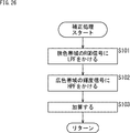
- FIG. 24 is a block diagram illustrating a configuration example of a correction unit in FIG. 23. 24 is a flowchart for describing imaging processing of the electronic device in FIG.
- amendment part of FIG. It is a figure explaining the structural example which provides a white pixel or the pixel for phase difference detection in a subblock. It is a figure explaining the example of an output timing of the pixel signal from an image sensor. It is a figure explaining the example which makes a column AD conversion part multistage. It is a figure explaining the variation of the pixel arrangement example. It is a figure explaining the variation of the pixel arrangement example. It is a figure explaining the variation of the pixel arrangement example. It is a figure explaining the variation of the pixel arrangement example. It is a figure explaining the variation of the pixel arrangement example. It is a figure explaining the variation of the pixel arrangement example.
- First Embodiment (1-1) Pixel Arrangement (FIGS. 1 to 4) (1-2) Configuration Example of First Embodiment of Electronic Device (FIGS. 5 and 6) (1-3) Imaging processing by electronic device of FIG. 5 (FIG. 7) 2.
- Second Embodiment (2-1) Simultaneous imaging of high frame rate imaging and normal frame rate imaging (FIG. 8) (2-2) Dynamic range expansion imaging ( Figure 9) (2-3) Configuration Example of Electronic Device according to Second Embodiment (FIG. 10) (2-4) Imaging processing by electronic device of FIG. 10 (FIG. 11) 3.
- Third Embodiment (3-1) Pixel Arrangement Example Composed of Normal Addition Pixel and Phase Difference Detection Pixel (FIGS.
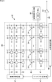
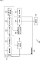
- FIG. 1 is a block diagram illustrating a configuration example of an embodiment of an image sensor to which the present technology is applied.
- a timing control unit 42 includes a timing control unit 42, a vertical scanning circuit 43, a pixel array 44, a constant current source circuit unit 45, a reference signal generation unit 46, and a column AD (Analog to Digital) on a semiconductor substrate (not shown). ) It is configured by providing the conversion unit 47. Further, a horizontal scanning circuit 48, a horizontal output line 49, and an output circuit 50 are provided.
- the timing control unit 42 supplies a clock signal and a timing signal necessary for a predetermined operation to the vertical scanning circuit 43 and the horizontal scanning circuit 48 based on a master clock having a predetermined frequency. For example, the timing control unit 42 supplies timing signals for the shutter operation and readout operation of the pixel 51 to the vertical scanning circuit 43 and the horizontal scanning circuit 48. Although not shown, the timing control unit 42 also supplies a clock signal and timing signal necessary for a predetermined operation to the reference signal generation unit 46, the column AD conversion unit 47, and the like.
- the vertical scanning circuit 43 sequentially supplies a signal for controlling the output of the pixel signal to each pixel 51 arranged in the vertical direction of the pixel array 44 at a predetermined timing.
- a plurality of pixels 51 are arranged in a two-dimensional array (matrix) in the pixel array 44. That is, M ⁇ N pixels 51 are arranged in a plane.
- the values of M and N are arbitrary integers.
- the plurality of pixels 51 arranged in a two-dimensional array are connected to the vertical scanning circuit 43 in units of rows by horizontal signal lines 52.
- the plurality of pixels 51 arranged in the same row in the pixel array 44 are connected to the vertical scanning circuit 43 by the same single horizontal signal line 52.
- the horizontal signal line 52 is shown as one wiring, but the number is not limited to one.
- the plurality of pixels 51 arranged in a two-dimensional array are connected to the horizontal scanning circuit 48 in units of columns by vertical signal lines 53.
- the plurality of pixels 51 arranged in the same column in the pixel array 44 are connected to the horizontal scanning circuit 48 by the same single vertical signal line 53.
- Each pixel 51 in the pixel array 44 outputs, to the vertical signal line 53, a pixel signal corresponding to the charge accumulated therein in accordance with a signal supplied from the vertical scanning circuit 43 via the horizontal signal line 52.
- the pixel 51 functions as an imaging pixel that outputs a pixel signal of an image of a subject. The detailed configuration of the pixel 51 will be described later with reference to FIG.
- the constant current source circuit unit 45 has a plurality of load MOS (Metal-Oxide Semiconductor) 54, and one load MOS 54 is connected to one vertical signal line 53.
- the load MOS 54 has a gate applied with a bias voltage and a source grounded, and forms a source follower circuit with a transistor in the pixel 51 connected via the vertical signal line 53.
- the reference signal generation unit 46 includes a DAC (Digital-to-Analog-Converter) 46a, generates a ramp (RAMP) waveform reference signal in accordance with the clock signal from the timing control unit 42, and generates a column signal. This is supplied to the AD conversion unit 47.
- DAC Digital-to-Analog-Converter
- the column AD conversion unit 47 has a plurality of ADCs (Analog-to-Digital Converters) 55, one for each column of the pixel array 44. Therefore, a plurality of pixels 51, one load MOS 54 and ADC 55 are connected to one vertical signal line 53.
- ADCs Analog-to-Digital Converters
- the ADC 55 performs a CDS (Correlated Double Sampling) process on the pixel signal supplied from the pixel 51 in the same column via the vertical signal line 53, and further performs an AD conversion process.
- CDS Correlated Double Sampling
- Each ADC 55 temporarily stores the pixel data after AD conversion and outputs it to the horizontal output line 49 according to the control of the horizontal scanning circuit 48.
- the horizontal scanning circuit 48 sequentially outputs the pixel data stored in the plurality of ADCs 55 to the horizontal output line 49 at a predetermined timing.
- the horizontal output line 49 is connected to an output circuit (amplifier circuit) 50, and pixel data after AD conversion output from each ADC 55 is output from the output circuit 50 to the outside of the image sensor 41 via the horizontal output line 49. Is output.
- the output circuit 50 signal processing unit
- the imaging device 41 configured as described above is a CMOS image sensor called a column AD system in which ADCs 55 that perform CDS processing and AD conversion processing are arranged for each vertical column.
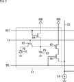
- FIG. 2 shows an equivalent circuit of the pixel 51.
- the pixel 51 includes a photodiode 61 as a photoelectric conversion element, a transfer transistor 62, an FD (Floating Diffusion: floating diffusion region) 63, a reset transistor 64, an amplification transistor 65, and a selection transistor 66.
- the photodiode 61 is a photoelectric conversion unit that generates and accumulates charges (signal charges) corresponding to the amount of received light.
- the photodiode 61 has an anode terminal grounded and a cathode terminal connected to the FD 63 via the transfer transistor 62.
- the transfer transistor 62 When the transfer transistor 62 is turned on by the transfer signal TX, the charge generated by the photodiode 61 is read and transferred to the FD 63.
- the FD 63 holds the electric charge read from the photodiode 61.
- the reset transistor 64 is turned on by the reset signal RST, the charge stored in the FD 63 is discharged to the constant voltage source VDD, thereby resetting the potential of the FD 63.
- the amplification transistor 65 outputs a pixel signal corresponding to the potential of the FD 63. That is, the amplification transistor 65 constitutes a load MOS 54 as a constant current source and a source follower circuit, and a pixel signal indicating a level corresponding to the charge accumulated in the FD 63 is sent from the amplification transistor 65 to the ADC 55 via the selection transistor 66. Is output.
- the selection transistor 66 is turned on when the pixel 51 is selected by the selection signal SEL, and outputs the pixel signal of the pixel 51 to the ADC 55 via the vertical signal line 53.
- the transfer signal TX, the reset signal RST, and the selection signal SEL are supplied from the vertical scanning circuit 43 via the horizontal signal line 52 (FIG. 1).
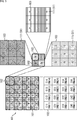
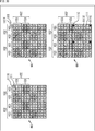
- FIG. 3 is a diagram illustrating a planar configuration example of an embodiment of an image sensor to which the present technology is applied. Specifically, FIG. 3 shows an arrangement of the pixels 51. That is, in the present embodiment, the pixel array 44 captures an image of the subject by the imaging region 101.
- the imaging area 101 includes a plurality of blocks 102 arranged in a matrix of M / 3 ⁇ N / 3.
- This block 102 constitutes a unit of an image to be captured. That is, the subject is imaged as a set of units of a predetermined color (a color synthesized by the colors of red (R), green (G), and blue (B)) for each block 102 and displayed (that is, the eyes of the human). Recognized).
- a predetermined color a color synthesized by the colors of red (R), green (G), and blue (B)
- the block 102 is configured by arranging the sub-blocks 103 in a Bayer array. That is, the block 102 includes four sub-blocks 103 including one red (R) sub-block 103, two green (G) sub-blocks 103, and one blue (B) sub-block 103. They are arranged in a 2 ⁇ 2 matrix.
- the color arrangement is not limited to the Bayer arrangement, but may be a stripe arrangement, a checkered arrangement, an interline arrangement, or the like.
- a green (G) sub-block 103 is arranged at the upper right and lower left of the block 102, a red (R) sub-block 103 is arranged at the upper left, and a blue (B) sub-block 103 is arranged at the lower right.
- the arrangement pattern of the sub-blocks 103 is the same.
- red (R), green (G), and blue (B) sub-blocks 103 will be referred to as R sub-block 103, G sub-block 103, and B sub-block 103, respectively, as necessary. To do.
- each region corresponding to a plurality of blocks 102 arranged in a matrix of M / 3 ⁇ N / 3 is represented by RNij (i, j are the row and column positions of block 102. Express).
- the color of the subject is captured and expressed as a color Cij for each region RNij.
- the synthesized color Cij is imaged as the color of the region RNij of the subject.
- the sub-block 103 is composed of 3 ⁇ 3 matrix-like pixels 111 of the same color that are adjacent to each other.
- the pixel 111 corresponds to the pixel 51 in FIGS. 1 and 2.
- the red (R), green (G), and blue (B) pixels 111 are referred to as an R pixel 111, a G pixel 111, or a B pixel 111, respectively, as necessary.
- the R sub-block 103 is composed of 3 ⁇ 3 matrix R pixels 111.
- the G sub-block 103 includes 3 ⁇ 3 matrix G pixels 111.
- the B sub-block 103 is composed of 3 ⁇ 3 matrix B pixels 111.
- the 3 ⁇ 3 pixels 111 of the same color constituting one sub-block 103 can be read out independently, but can also be read out collectively as one sub-block 103.
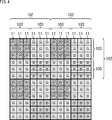
- FIG. 4 is a diagram illustrating a planar configuration example of an embodiment of an imaging device to which the present technology is applied. That is, when the imaging region 101 in FIG. 3 is expressed by the pixels 111, it is as shown in FIG.
- One sub-block 103 is composed of 3 ⁇ 3 pixels 111 of the same color. Specifically, one R sub-block 103 is composed of 3 ⁇ 3 R pixels 111. Similarly, one G sub-block 103 is composed of 3 ⁇ 3 G pixels 111, and one B sub-block 103 is composed of 3 ⁇ 3 B pixels 111.
- one block 102 is composed of 3 ⁇ 3 sub-blocks 103 (one R sub-block 103, two G sub-blocks 103, and one B sub-block 103).
- the sub-block 103 is configured by a plurality of pixels 111 of the same color, and the block 102 is configured by a plurality of sub-blocks 103 including different colors. Then, as a combined color of the block 102 in which different colors of the plurality of sub-blocks 103 are combined, a person recognizes it as the color of the imaging point of the subject at the position corresponding to the block 102.
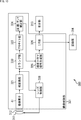
- FIG. 5 is a diagram illustrating a configuration example of the first embodiment of an electronic device to which the present technology is applied.
- An electronic device 300 shown in FIG. 5 is a device that images a subject and outputs an image of the subject as an electrical signal.
- the electronic device 300 is configured as, for example, a compact digital camera, a digital single-lens reflex camera, a video camera, a mobile terminal such as a smartphone (multifunctional mobile phone) having an imaging function, an endoscope, or the like.
- the imaging control unit 301 includes an imaging element 41, an AD conversion unit 321, a clamp unit 322, a demosaic unit 323, a linear matrix (LM) / white balance (WB) / gamma correction unit 324, a luminance chroma signal generation unit 325, an interface (I / F) section 326 and a lens control section 328.
- the display unit 313 and the recording unit 314 are provided outside the imaging control unit 301, but may be provided inside.
- the lens 311 adjusts the focal length of the subject light incident on the image sensor 41.
- a stop (not shown) that adjusts the amount of subject light incident on the image sensor 41 is provided at the subsequent stage of the lens 311.
- the specific configuration of the lens 311 is arbitrary.
- the lens 311 may be configured by a plurality of lenses.
- the subject light transmitted through the lens 311 is incident on the image sensor 41 via an optical filter 312 configured as an IR cut filter that cuts infrared light and transmits light other than infrared light, for example.
- an optical filter 312 configured as an IR cut filter that cuts infrared light and transmits light other than infrared light, for example.
- the imaging device 41 includes a plurality of pixels 111 having photoelectric conversion elements such as photodiodes that photoelectrically convert subject light. Each pixel 111 converts subject light into an electrical signal, and supplies the electrical signal to the AD conversion unit 321.
- the imaging element 41 constitutes a solid-state imaging device of the present technology.
- This solid-state imaging device may be configured as a single-chip module, or the imaging device 41 and the signal processing circuit may be configured as separate chips.
- the imaging device 41 of the present technology is, for example, a CCD image sensor that performs transfer using a circuit element called a charge-coupled device (CCD (Charge-Coupled Device)) in order to read out the electric charge generated by the photoelectric conversion device based on subject light.
- CCD Charge-Coupled Device
- CMOS image sensor using an amplifier for each unit cell using a CMOS (Complementary Metal Metal Oxide Semiconductor) may be used.
- the AD conversion unit 321 converts the RGB electrical signal (analog signal) supplied from the image sensor 41 into digital data (image data).
- the AD conversion unit 321 supplies the image data (RAW data) of the digital data to the clamp unit 322 and the lens control unit 328.
- the clamp unit 322 subtracts a black level that is a pixel value of the non-image output area and is determined to be black from the image data.
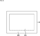
- FIG. 6 is a diagram illustrating an image output area and a non-image output area to which the present technology is applied.
- the pixel array 44 is provided with an image output area 44 ⁇ / b> A substantially at the center thereof, and a non-image output area 44 ⁇ / b> B is provided around the image output area 44 ⁇ / b> B.
- the image output area 44A is an effective pixel area, and the output of the pixel 111 in the image output area 44A is used as image data.
- the output of the pixel 111 in the non-image output area 44B is not used as image data.
- an OPB (Optical Black) region is set for the pixel 111 in the non-image output region 44B, and the output of the pixel 111 in the OPB region is set to a black level that is determined to be black.
- the clamp unit 322 supplies the demosaic unit 323 with all pixels of the image data obtained by subtracting the black level that is the output of the pixel 111 in the OPB area.
- the lens control unit 328 controls the driving of the lens 311. Specifically, the lens control unit 328 calculates the driving amount of the lens 311 according to the focus determination result based on the focus determination by contrast autofocus using the image data from the AD conversion unit 321, The lens 311 is moved according to the calculated drive amount.
- the demosaic unit 323 performs demosaic processing on the RAW data from the AD converter 321, performs color information complementation, etc., and converts the data into RGB data.
- the demosaic unit 323 supplies image data (RGB data) after demosaic processing to the LM / WB / gamma correction unit 324.
- the LM / WB / gamma correction unit 324 corrects the color characteristics of the RGB data from the demosaic unit 323. Specifically, the LM / WB / gamma correction unit 324 uses image data using a matrix coefficient to fill in the difference between the chromaticity point of the primary color (RGB) defined in the standard and the chromaticity point of the actual camera. Each color signal is corrected to change the color reproducibility. The LM / WB / gamma correction unit 324 adjusts the white balance by setting a gain for white for each channel value of RGB data.
- the LM / WB / gamma correction unit 324 performs gamma correction to obtain a display closer to the original by adjusting the relative relationship between the color of the image data and the output device characteristics.
- the LM / WB / gamma correction unit 324 supplies the corrected image data (RGB data) to the luminance chroma signal generation unit 325.
- the luminance chroma signal generation unit 325 generates a luminance signal (Y) and a color difference signal (Cr, Cb) from the RGB data supplied from the LM / WB / gamma correction unit 324.
- the luminance chroma signal generation unit 325 generates the luminance chroma signal (Y, Cr, Cb)
- the luminance chroma signal and the color difference signal are supplied to the I / F unit 326.
- the I / F unit 326 supplies the supplied image data (luminance chroma signal) to a recording unit 314 such as a recording device that records the image data, and records the image data or displays an image of the image data.
- the data is output to the display unit 313 and displayed.
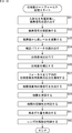
- FIG. 7 is a flowchart for describing imaging processing of an electronic device to which the present technology is applied.
- step S ⁇ b> 11 the image sensor 41 photoelectrically converts the incident light of each pixel 111, reads out the pixel signal, and supplies it to the AD converter 321.
- step S ⁇ b> 12 the AD conversion unit 321 AD-converts each pixel signal from the image sensor 41 and supplies it to the clamp unit 322.
- step S13 the clamp unit 322 subtracts the black level detected in the OPB (Optical Black) region provided outside the effective pixel region from each pixel signal (pixel value) from the AD conversion unit 321.
- the clamp unit 322 supplies image data (pixel values) for all pixels from which the black level has been subtracted to the demosaic unit 323.
- step S14 the demosaic unit 323 performs demosaic processing, converts the RAW data into RGB data, and supplies the RGB data to the LM / WB / gamma correction unit 324.
- step S15 the LM / WB / gamma correction unit 324 performs color correction, white balance adjustment, and gamma correction on the RGB data from the demosaic unit 324, and supplies the result to the luminance chroma signal generation unit 325.
- step S16 the luminance chroma signal generation unit 325 generates a luminance signal and a color difference signal (that is, YCrCb data) from the RGB data.
- step S17 the I / F unit 326 outputs the luminance signal and the color difference signal generated by the luminance chroma signal generation unit 325 to the recording unit 314 and the display unit 313.
- step S18 the display unit 313 displays an image of the subject based on the signal supplied from the I / F unit 326. Further, the recording unit 314 records the signal supplied from the I / F unit 326 based on an instruction from the user.
- the subject at the position corresponding to the block 102 is obtained as the combined color of the block 102 in which different colors are combined in units of the sub-block 103 composed of 3 ⁇ 3 pixels 111 of the same color. It can be recognized by a person as the color of the imaging point.
- Second Embodiment> (2-1) Simultaneous Imaging with High Frame Rate Imaging and Normal Frame Rate Imaging
- the exposure times of the pixels 111 constituting the sub-block 103 may not all be the same.
- the pixel at the center position in the sub-block 103 marked with a white star is a single pixel.
- the other eight pixels 111 may be read out as normal pixels.
- pixel signals read from eight normal pixels 111 may be added and used as a pixel signal of one pixel.
- the normal addition pixel when the exposure time ( ⁇ frame rate) of the single pixel 111A is, for example, eight times as long as the normal pixel 111, the normal addition pixel is Therefore, it can be treated as a pixel having a sensitivity of 8 times that of the normal pixel 111.
- pixel signals are handled in units of sub-blocks 103, in this example, pixel signals of normal addition pixels and pixel signals of single pixels 111A exist in the same sub-block 103. .
- the normal addition pixel has the same sensitivity as that of the single pixel 111A even if the frame rate is 480 fps. It becomes possible to do.
- the upper stage in the lower part of FIG. 8 shows the readout timing of the normal addition pixel, and shows the exposure start time and the exposure end time of each. Further, the lower part of FIG. 8 shows the readout timing of the single pixel 111A, and shows the exposure start time and the exposure end time.
- the exposure of the first frame of the normal addition pixels starts at time t0 and ends at time t1.
- the exposure of the second frame of the normal addition pixels starts at time t1 and ends at time t2.
- exposure starts at time t2, and exposure ends at time t3.
- exposure starts at time t3, and exposure ends at time t4.
- exposure starts at time t4, and exposure ends at time t5.
- the exposure of the sixth frame of the normal addition pixels starts at time t5 and ends at time t6.
- exposure starts at time t6, and exposure ends at time t7.
- time t7 In the eighth frame of the normal addition pixels, exposure starts at time t7, and exposure ends at time t8. Note that time t1 to t2, time t2 to t3, time t3 to t4, time t4 to t5, time t5 to t6, time t6 to t7, and time t7 to t8 are all the same time.
- the single pixel 111A starts exposure at the time t0 for the first frame, and the exposure ends at the time t8.
- the normal addition pixel can realize imaging with the same sensitivity at the frame rate of 8 times that the sensitivity is 8 times that of the single pixel 111A.
- the upper left part and upper right part of FIG. 9 are the same as that of FIG.
- the upper row shows normal addition pixels
- the lower row shows the exposure start time and exposure end time of the single pixel 111 ⁇ / b> A, both of which start exposure at time t ⁇ b> 11 and exposure at time t ⁇ b> 12. Is shown to have ended.
- HDR imaging is realized by changing the exposure time for each pixel.
- the exposure timing differs in units of pixels, if there is movement in the subject, pixel signals in which different subjects are reflected can be obtained between pixels with different exposure times. Therefore, motion blur occurs and the image quality is reduced.
- HDR imaging can be realized using pixel signals exposed at the same timing using normal addition pixels and single pixels 111A having different sensitivities.
- normal addition pixels and single pixels 111A having different sensitivities.
- motion blur is reduced even in HDR imaging. It becomes possible to make it.
- the same reference numerals and the same names are given to the components having the same functions as those of the electronic device 300 of FIG. 4, and the description thereof is omitted as appropriate.
- the electronic device 300 in FIG. 10 is different from the electronic device 300 in FIG. 5 in that a clamp unit 330 is provided instead of the clamp unit 322.
- the basic function of the clamp unit 330 is the same as that of the clamp unit 322. Further, the digital signal of the pixel signal supplied from the normal pixel 111 is added, and one normal addition pixel is sub-block 103 unit. For the single pixel 111A, the pixel signal as it is is treated as a pixel signal of one pixel of the sub-block 103 at the same position.
- steps S21, S22, S24 to S29 in the flowchart of FIG. 10 are the same as those in steps S11 to S18 in the flowchart of FIG.
- the processing in steps S21 and S22 is processing performed in each of the eight pixels 111 that normally constitute the addition pixel.
- step S23 the clamp unit 330 adds the eight pixel values constituting the normal addition pixel to each pixel signal (pixel value) from the AD conversion unit 321. Signal processing is executed as normal addition pixels.
- the imaging process using the single pixel 111A is the same as the process described with reference to the flowchart of FIG.
- the normal addition pixel and the single pixel 111A having different sensitivities in the sub-block 103 unit the same sensitivity can be obtained even if the normal addition pixel and the single pixel 111A have different exposure times. Therefore, for example, it is possible to simultaneously realize high frame rate imaging with the same sensitivity and normal frame rate imaging.
- the normal addition pixel when the sensitivity of the normal addition pixel is 8 times the sensitivity of the single pixel 111A, the normal addition pixel has a frame rate (1/8 exposure time) that is 8 times that of the single pixel 111A. ), An image with the same sensitivity can be captured. As a result, it is possible to realize imaging at different frame rates at the same time.
- the configuration for processing the pixel signal of the normal addition pixel and the configuration for processing the pixel signal of the single pixel 111 may be independent of each other. That is, for example, with respect to the clamp unit 330, the demosaic unit 323, the LM / WB / gamma correction unit 324, the luminance chroma signal generation unit 325, and the interface unit 326, each of which processes the pixel signal of the normal addition pixel and the single pixel 111, respectively. It is also possible to provide two systems independently of those that process the pixel signals.
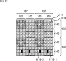
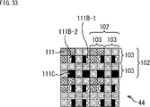
- m ⁇ n pixels 111 are basically R, G, and B imaging pixels, but the horizontal direction 3 ⁇ vertical direction 3 constituting the sub-block 103.
- the pixel at the center position in the horizontal direction and at the center position in the vertical direction is replaced with one of the pair of phase difference detection pixels 111B-1 and 111B-2.
- one of the phase difference detection pixels 111B-1 and 111B-2 is regularly arranged throughout.
- a plurality of phase difference detections in which half of the pixels are indicated by black rectangles and the other half are indicated by white stars.
- the pixels 111B-1 or 111B-2 are arranged in a scattered manner.
- the center pixel 111 at the relatively same position (corresponding position) among the 3 ⁇ 3 pixels 111 is detected by the phase difference detection.
- the pixel 111B-1 or 111B-2 is used.
- phase difference detection pixels 111B-1 and 111B-2 that detect the phase difference in the horizontal direction
- the phase difference detection pixels 111B-1 is arranged.
- phase difference detection pixels 111B-2 constituting the other of the pair detecting the phase difference in the horizontal direction are arranged.
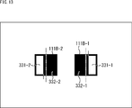
- FIG. 13 is a diagram illustrating a configuration of the phase difference detection pixels 111B-1 and 11B-2 of the pixel array 44 of the image sensor 41 to which the present technology is applied.
- the left side of FIG. 13 shows the phase difference detection pixel 111B-2 of the pair of phase difference detection pixels 111B-1 and 111B-2 that detect the phase difference in the horizontal direction.
- a light shielding portion 332-2 is formed on the right side thereof, and a light transmitting portion 331-2 is formed on the left side thereof.
- the light shielding portion 332-2 that shields light from the subject toward the photodiode 61 is formed of a metal film such as copper, for example.
- the light transmitting portion 331-2 that transmits light from the subject toward the photodiode 61 is formed by opening a part of the metal film forming the light shielding portion 332-2.
- the opening can be formed by not forming the light shielding portion 332-2.
- the light shielding portion 332-1 is on the left side and the light transmitting portion 331 is on the right side. -1 is formed.
- the light shielding portion 332-1 that shields light from the subject toward the photodiode 61 is formed of, for example, a metal film such as copper, and the light transmitting portion 331 that transmits light from the subject toward the photodiode 61.
- ⁇ 1 is formed by opening a part of the metal film forming the light shielding portion 332-1.
- it is also possible to form an opening by not forming the light shielding portion 332-1.
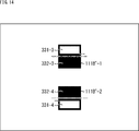
- FIG. 13 shows an example in which a phase difference detection pixel 111B for detecting a phase difference in the horizontal direction (horizontal direction) is provided, the phase difference in the vertical direction (vertical direction) may be detected. Good.
- FIG. 14 shows the phase difference detection pixel 111B′-1 of the pair of phase difference detection pixels 111B′-1 and 111B′-2 that detect the phase difference in the vertical direction.
- a light shielding portion 332-3 is formed below and a light transmitting portion 331-3 is formed above.
- the light shielding portion 332-3 that shields light from the subject toward the photodiode 61 is formed of, for example, a metal film such as copper, and the light transmitting portion 331-1 that transmits light from the subject toward the photodiode 61. 3 is formed by opening a part of the metal film forming the light shielding portion 332-4. Of course, it is also possible to form an opening by not forming the light shielding portion 332-3.
- the light shielding portion 332-4 is on the upper side and the light shielding portion 332-4 is on the lower side.
- a light transmitting portion 331-4 is formed.
- the light shielding portion 332-4 that shields light from the subject toward the photodiode 61 is formed of a metal film such as copper, for example, and transmits light from the subject toward the photodiode 61. 4 is formed by opening a part of the metal film forming the light shielding portion 332-4. Of course, it is also possible to form an opening by not forming the light shielding portion 332-4.
- FIG. 15 is a cross-sectional view illustrating a configuration example of a normal pixel 111 according to an embodiment of an image sensor to which the present technology is applied.
- FIG. 15 illustrates a cross-sectional configuration of two pixels 111 among the pixels constituting the normal addition pixel.
- a photodiode 352 (corresponding to the photodiode 61 in FIG. 2) as a photoelectric conversion unit is formed on a Si (silicon) semiconductor substrate 351.
- An R, G, or B color filter 354 is formed on the upper layer of the semiconductor substrate 351, and an on-chip lens 355 is formed on the upper layer thereof.
- the light from the subject is collected by the on-chip lens 355, passes through the R, G, or B color filter 354, and the light of the color corresponding to the color filter 354 is incident on the photodiode 352.
- a color signal (pixel signal) of a light component of a color corresponding to the color filter 354 is output from the photodiode 352.
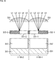
- FIG. 16 is a cross-sectional view illustrating a configuration example of a phase difference detection pixel according to an embodiment of an imaging device to which the present technology is applied.
- FIG. 16 shows the cross-sectional configurations of two phase difference detection pixels 111B-1 and 111B-2 side by side for convenience.
- the configuration of the phase difference detection pixel 111B is basically the same as that of the pixel 111 shown in FIG. 15.
- the color filter 354 shown in FIG. 332-1 and translucent parts 331-1 and 331-2 are arranged.
- the configurations of the light shielding units 332-1 and 332-2 and the light transmitting units 331-1 and 331-2 are as described with reference to FIGS.
- phase difference detection pixel 111B-2 a part of the light condensed by the on-chip lens 355 is transmitted through the light transmitting portion 331-2 and is incident on the photodiode 352.
- a part of the light collected by the on-chip lens 355 is shielded by the light shielding part 332-2 arranged on the right side of the light transmitting part 331-2 in FIG. 16, and does not enter the photodiode 352.
- phase difference detection pixel 111B-1 a part of the light condensed by the on-chip lens 355 passes through the light transmitting portion 331-1 and enters the photodiode 352.
- a part of the light collected by the on-chip lens 355 is shielded by the light shielding part 332-1 disposed on the left side of the light transmitting part 331-1 in FIG. 16, and does not enter the photodiode 352.
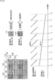
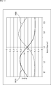
- FIG. 17 is a diagram for explaining the phase difference characteristics of the phase difference detection pixel according to the embodiment of the imaging device to which the present technology is applied. Hereinafter, the principle of phase difference detection will be described with reference to FIGS. 16 and 17.
- phase difference detection pixels 111B-1 and 111B-2 As shown in FIG. 16, it is assumed that incident light L1 to L5 from five directions is incident on the phase difference detection pixels 111B-1 and 111B-2.
- the graph of FIG. 17 shows pixel signal outputs of the phase difference detection pixels 111B-1 and 111B-2 at that time.
- the horizontal axis indicates the incident angle of the incident light
- the vertical axis indicates the pixel signal output of the phase difference detection pixels 111B-1 and 111B-2.
- a solid line 141B indicates the pixel signal output of the phase difference detection pixel 111B-1
- a broken line 141A indicates the pixel output of the phase difference detection pixel 111B-2.
- the left-side light-shielded phase difference detection pixel 111B-1 has a larger output when the angle of incident light is set on the left side (minus side), and the right-side light-shielded phase difference detection pixel 111B.
- the output of -2 increases when the angle of incident light is set on the right side (plus side). That is, when the angle component in the negative direction is large in the incident light as in the incident light L1, the output of the phase difference detection pixel 111B-1 is larger than the output of the phase difference detection pixel 111B-2.
- the pixel signal output of the phase difference detection pixel 111B-2 is larger than the pixel signal output of the phase difference detection pixel 111B-1.
- the defocus amount is detected by using the phase difference characteristics of the pixel signal output of each of the phase difference detection pixels 131 with respect to the incident angle of the incident light.
- FIG. 18 is a diagram illustrating a configuration example of a third embodiment of an electronic device to which the present technology is applied.
- configurations having the same functions as those of the electronic device 300 in FIG. 10 are denoted by the same names and the same reference numerals, and description thereof will be omitted as appropriate.
- the electronic device 300 in FIG. 18 is different from the electronic device 300 in FIG. 10 in that a correction parameter calculation unit 371, a memory 372, a phase difference correction unit 373, a phase difference detection unit 374, and a lens control unit 375 are further provided. It is a point.
- the correction parameter calculation unit 371 calculates a correction parameter using phase difference characteristic data obtained in a test process after the image sensor 41 is manufactured, a test process after the lens 311 is attached to the image sensor 41, and the like. This correction parameter is used to correct the phase difference detected by the phase difference detector 374.
- the memory 372 stores the correction parameters calculated by the correction parameter calculation unit 371.
- the phase difference detection unit 374 performs the phase difference detection process based on the image data (pixel value) from the clamp unit 330, thereby determining whether or not the object to be focused (focused object) is in focus. To determine. When the object in the focus area is in focus, the phase difference detection unit 374 supplies information indicating that the object is in focus to the lens control unit 375 as a focus determination result. The phase difference detection unit 373 calculates the amount of focus shift (defocus amount) when the focused object is not in focus, and uses the information indicating the calculated defocus amount as the focus determination result. To the lens control unit 375.
- the phase difference correction unit 373 corrects the phase difference detected by the phase difference detection unit 374 using the correction parameter stored in the memory 372.
- the phase difference detection unit 374 supplies a focus determination result corresponding to the corrected phase difference to the lens control unit 375.
- the lens control unit 375 controls the driving of the lens 311. Specifically, the lens control unit 375 calculates the driving amount of the lens 311 based on the focus determination result supplied from the phase difference detection unit 374, and moves the lens 311 according to the calculated driving amount. .
- the lens control unit 375 maintains the current position of the lens 311 when in focus.
- the lens control unit 375 calculates a drive amount based on the focus determination result indicating the defocus amount and the position of the lens 311, and moves the lens 311 according to the drive amount. Move.
- phase difference autofocus processing by the electronic apparatus 300 in FIG. 18 will be described with reference to the flowchart in FIG.
- the phase difference autofocus process is executed by the electronic device 300 before or in parallel with the imaging process when the subject is imaged.
- step S ⁇ b> 31 the image sensor 41 photoelectrically converts incident light of each pixel 111, reads each pixel signal, and supplies it to the AD conversion unit 321.
- the phase difference detection pixel 111B may be read at a timing different from that of the normal pixel 111.
- step S ⁇ b> 32 the AD conversion unit 321 AD-converts each pixel signal from the image sensor 41 and supplies the converted signal to the clamp unit 322.
- step S33 the clamp unit 322 subtracts the black level detected in the OPB (Optical Black) region provided outside the effective pixel region from each pixel signal (pixel value) from the AD conversion unit 321.
- the clamp unit 322 supplies the image data (pixel value) output from the phase difference detection pixel 111B to the phase difference detection unit 374 among the image data obtained by subtracting the black level.
- step S34 the phase difference correction unit 373 reads a correction parameter calculated in advance and stored in the memory 372.
- step S35 the phase difference detection unit 374 performs phase difference detection based on the image data (pixel value) from the clamp unit 322. That is, the output of the phase difference detection pixel 111B that detects the phase difference between the vertical direction (vertical direction) and the horizontal direction (horizontal direction) is read out.
- step S36 the phase difference correction unit 373 corrects the phase difference detected by the phase difference detection unit 374 using the correction parameter read in the process of step S44. That is, the correction parameter is supplied to the phase difference detection unit 374, and the detected phase difference is corrected.
- step S37 the phase difference detection unit 374 connects the outputs of the phase difference detection pixels 131 in the focus area. That is, the outputs of the phase difference detection pixels 111B in the focus area are connected according to the pixel position, and an AF pixel signal is generated.
- step S38 the phase difference detection unit 374 performs a shading correction (peripheral screen light amount drop correction), a two-image distortion restoration correction by vignetting, and the like on the AF pixel signal generated in step S37, and performs correlation calculation. A pair of image signals is generated.
- a shading correction peripheral screen light amount drop correction
- a two-image distortion restoration correction by vignetting and the like
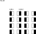
- FIG. 20 is a diagram illustrating a configuration of the phase difference detection pixels 111B-1 and 111B-2 according to the embodiment of the imaging device to which the present technology is applied.
- the image sensor 41 of the present embodiment includes a phase difference detection pixel 111B-2 for detecting a phase difference in the horizontal direction and a phase difference in the horizontal direction paired therewith. And a phase difference detection pixel 111B-1 for detection.
- the signal of the phase difference detection pixel 111B is grouped. As shown in FIG. 20, the phase difference detection pixels 111B-1 and 111B-2 for detecting the phase difference in the horizontal direction are grouped in the horizontal direction, for example, in the second row, the eighth row, and so on. It becomes.
- the image signal SIGh (A for phase difference detection obtained by connecting the pixel signals obtained in the phase difference detection pixel 111B-2 included in the focus area Rh for phase difference detection in the horizontal direction in the horizontal direction. ) Is generated.
- an image signal SIGh (B) for phase difference detection is generated by horizontally connecting pixel signals obtained by the phase difference detection pixels 111B-1 included in the focus area Rh.
- step S39 the phase difference detection unit 374 calculates the correlation of the image signal pair for phase difference detection. That is, the correlation of the phase difference between the image signal SIGh (A) and the image signal SIGh (B) is calculated.
- step S40 the phase difference detection unit 374 determines the reliability of the correlation. That is, the reliability of the correlation calculation result calculated in step S39 is determined.
- the reliability refers to the degree of coincidence of image signal pairs (similarity between waveforms). When the degree of coincidence is good, the reliability of the focus detection result is generally high.
- the defocus amount in the horizontal direction can be obtained.
- step S41 the phase difference detection unit 374 calculates a defocus amount. That is, in step S40, the final defocus amount is calculated based on the phase difference obtained from the image signal pair determined to be highly reliable.
- step S42 the lens control unit 375 controls the driving of the lens 311 based on the focus determination result from the phase difference detection unit 374.
- the lens control unit 375 may control the driving of the lens 311 by performing contrast autofocus in addition to the phase difference autofocus as described above. For example, when information indicating a focus shift amount (defocus amount) is supplied as a focus determination result from the phase difference detection unit 374, the lens control unit 375 receives the focus shift direction (front pin or rear pin). Or the contrast autofocus may be performed in that direction.
- the phase difference autofocus process is executed while reading the normal addition pixel from time t21 to t22.
- the center pixel is a phase difference detection pixel.
- 111B-1 and 111B-2 among the 3 pixels ⁇ 3 pixels constituting the lower sub-block 103, the central pixel is configured as a black pixel 111C.
- the central pixel is configured as the black pixel 111 ⁇ / b> C
- the lower pixel 102 constituting the lower sub-block 103 is composed of 3 pixels ⁇ 3 pixels.
- the center pixel is configured as phase difference detection pixels 111B-1 and 111B-2.
- the black pixel 111C is a pixel corresponding to a pixel configured to obtain a black level provided in the OPB area provided in the non-image output area 44B of FIG. More specifically, the black pixel 111C is a pixel whose entire surface is covered with the light shielding portion 332 formed of a metal film such as copper described with reference to FIG.
- the pixel signal of each pixel 111 in units of sub-blocks 103 reads the black level of the neighboring black pixel 111C, and the black in the processing of steps S13 (FIG. 7), S23 (FIG. 11), and S33 (FIG. 19) described above. Used for level subtraction.
- the pixel signals of the phase difference detection pixels 111B-1 and 111B-2 and the black pixel 111C are read from time t50 to t51, and thereafter From t51 to t52, the normal addition pixel is read out.
- phase difference detection pixels 111B-1 and 111B-2 are read first, and at the subsequent timing, the phase difference autofocus process is executed while reading the normal addition pixels,
- the focus adjustment by the lens 311 it is possible to perform continuous imaging while keeping the focus following the movement of the subject, and it is possible to suppress deterioration in image quality.
- the black level of the neighboring black pixel 111C is subtracted for each sub-block 103 by subtracting the black level using the black pixel that has been read first. Image quality can be improved.
- the pixels 111 in the OPB area set in the non-image output area 44B provided in the periphery of the image output area 44A in FIG. 6 have been set to the black level. Therefore, black that is generated two-dimensionally in the image output area 44A. Correction using level variation was not possible. However, by correcting the pixel signal using the two-dimensional black level detection result using the black pixel 111C of the present disclosure, it is possible to suppress the black level variation that occurs two-dimensionally, and to achieve higher accuracy. Clamping can be realized.
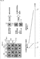
- the central pixel is configured as a white pixel 111 ⁇ / b> D.
- the white pixel 111 ⁇ / b> D is configured such that the transparent color filter 354 or the color filter 354 is not provided, and white light is incident on the photodiode 352.
- the pixel signals of the normal eight pixels 111 in the sub-block 103 unit are added, so that the normal addition pixels in the narrow color band of the Bayer array are added.
- a pixel signal is read out.
- the white pixel 111D outputs the luminance signal itself when white light is incident thereon.
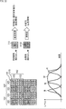
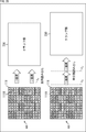
- the signals indicated by the waveforms R, G, B, and W are output from the normal addition pixels and the white pixels 111D of the RGB sub-blocks 103 as shown in the lower left part of FIG. Is done.
- the horizontal axis represents the wavelength
- the vertical axis represents the level of the pixel signal.
- the pixel signal of the normal addition pixel output from each of the RGB sub-blocks 103 in the Bayer array is a narrow color band signal, whereas the luminance signal output from the white pixel 111D is a wide color. Band signal.
- the pixel signal of the normal addition pixel output from each of the RGB sub-blocks 103 uses a narrow color band signal and a wide color band signal to reduce false resolution and high frequency color false.
- an LPF Low Pass Filter
- a narrow color band which is a pixel signal of a normal addition pixel output from each RGB sub-block 103, and a DC component of a color is obtained. Extracted.
- the wide color band signal output from the white pixel 111D is subjected to HPF (High Pass Filter) to extract an AC component of luminance.
- FIG. 23 is a diagram illustrating a configuration example of a fourth embodiment of an electronic device to which the present technology is applied.
- components having the same functions as those of the electronic device 300 in FIG. 18 are denoted by the same names and the same reference numerals, and description thereof will be omitted as appropriate.
- the electronic device 300 in FIG. 23 differs from the electronic device 300 in FIG. 18 in that a correction unit 391 is provided between the demosaic unit 323 and the LM / MB / gamma correction unit 324.
- the correction unit 391 extracts a DC component of the color by applying a LPF (Low Pass Filter) to the narrow color band signal, which is a pixel signal of the normal addition pixel output from each of the RGB sub-blocks 103, and white color
- LPF Low Pass Filter
- HPF High Pass Filter
- correction unit 391 A detailed configuration of the correction unit 391 will be described later with reference to FIG.
- FIG. 24 (4-3) Configuration Example of Correction Unit
- the upper part of FIG. 24 is a diagram showing a configuration example of the correction unit 391 of FIG. 23, and the lower part of FIG. 24 is the frequency and response output of the input signals of the HPF 401 and LPF 402. It is a wave form diagram which shows the relationship.
- the correction unit 391 includes an HPF (High Pass Filter) 401, an LPF (Low Pass Filter) 402, and an adder 403.
- HPF High Pass Filter
- LPF Low Pass Filter
- the HPF 401 extracts an AC component from the luminance signal supplied from the white pixel 111D of each of the RGB sub-blocks 103 and outputs the AC component to the adding unit 403.
- the LPF 402 extracts a DC component from the pixel signal from the normal addition pixel of each of the RGB sub-blocks 103 and outputs the DC component to the addition unit 403.
- the adder 403 adds the DC component of the pixel signal from the normal addition pixel of each RGB sub-block 103 from the LPF 402 and the AC component of the luminance signal from the HPF 401 to obtain the color signal of the RGB sub-block 103. Output as.
- the LPF 402 has a high response output when the frequency of the input signal is low, and a low response output when the frequency is high.
- the HPF 401 has a low response output when the frequency of the input signal is low, and a high response output when the frequency is high. That is, when the maximum value of the response output is 1, the response output of HPF 401 is a value obtained by subtracting the response output of LPF 402 from 1.
- the LPF 402 when the LPF 402 is applied to the pixel signal of the normal addition pixel of the RGB sub-block 103, the response output increases or decreases according to the RGB frequency.
- the extracted AC component By supplementing the extracted AC component, it is possible to suppress the occurrence of false resolution and color false.
- step S84 the clamp unit 330 subtracts the black level detected as the pixel signal of the corresponding black pixel 111C from the pixel signal (pixel value) of the normal addition pixel from the AD conversion unit 321 for each sub-block 103. .
- the clamp unit 330 supplies image data (pixel values) for all pixels from which the black level has been subtracted to the demosaic unit 323. That is, here, the black level, which is the pixel signal of the black pixel 111C, is subtracted from the pixel signal of the normal addition pixel in units of the sub-block 103.
- the two-dimensional black level variation that can occur in units of the pixels 111 on the pixel array 44 can be corrected with high accuracy.
- step S86 the correction unit 391 executes correction processing to extract the DC component of the pixel signal of the normal addition pixel of the RGB sub-block 103, and the AC component of the luminance signal of the corresponding white pixel 111D. By extracting and adding, generation of false resolution and color false is suppressed.
- step S101 the LPF 402 multiplies the narrow color band pixel signal corresponding to each of the RGB sub-blocks 103 in the Bayer array by applying the LPF, extracts the DC component of the color, and outputs it to the adder 403.
- step S102 the HPF 401 multiplies the luminance signal in the wide color band corresponding to each of the RGB sub-blocks 103 in the Bayer array by applying HPF, extracts the AC component of the luminance, and outputs it to the adding unit 403.
- step S ⁇ b> 103 the addition unit 403 adds the luminance AC component supplied from the HPF 401 and the color DC component supplied from the LPF 402 to each of the RGB sub-blocks 103 in the Bayer array, and outputs the result to the clamp unit 322. To do.
- the central pixel is configured as a white pixel 111D.
- the central pixel is constituted as a white pixel 111 ⁇ / b> D, and 3 pixels ⁇ 3 pixels constituting the lower sub-block 103.
- the center pixel is configured as phase difference detection pixels 111B-1 and 111B-2.
- Detection pixels 111B-1 and 111B-2 are respectively output. That is, two pairs of phase difference detection pixels 111B-1 and 111B-2 are arranged in units of 2 ⁇ 2 blocks 102.
- the pixel signal is read from the two pairs of phase difference detection pixels 111B-1 and 111B-2 so that phase difference autofocus processing is executed and the focus by the lens 311 is adjusted, and then the focus is adjusted. Since the normal image is read out by the normal addition pixel and the correction process using the white pixel 111D can be realized, it is possible to suppress the deterioration of the image quality.
- the output of the pixel signal from the image pickup device 41 is the pixel signal of the normal eight pixels 111 constituting the sub-block 103 and one pixel having some other function (hereinafter, functional pixel).
- functional pixel the pixel signal
- the pixel signals of the normal eight pixels 111 and the pixel signals of one other functional pixel 111X are output to the clamp unit 330 at the same timing. You may make it read in parallel.
- the clamp unit 322 adjusts the timing by buffering pixel signals having different processing timings. There is a need to.
- the functional pixel 111X is a generic term for the above-described single pixel 111A, phase difference detection pixels 111B-1, 111B-2, black pixel 111C, and white pixel 111D.
- the output may be performed in accordance with the processing order and timing.
- time division readout is performed so that the pixel signal of the normal pixel 111 is output at time tx and then the pixel signal of the functional pixel 111X is output at time ty. You may do it. Alternatively, the order may be changed, and after the pixel signal of the functional pixel 111X is output, the time division readout may be performed so that the pixel signal of the normal pixel 111 is output.
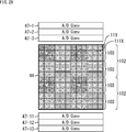
- the column AD conversion unit 47 is provided with one ADC 55 for each vertical signal line 53, and the configuration example in which AD conversion is performed for each row has been described.
- FIG. As shown in FIG. 4, the column AD conversion units 47-1 to 47-3 and 47-11 to 47-13 are provided for each of three rows in the vertical direction, and the block 102 in the upper half of the pixel array 44 is The AD conversion is performed by the column AD conversion units 47-1 to 47-3 provided in the upper part for every three columns of the pixels 111 as the unit of the subblock 103, and the lower block 102 of the pixel array 44 is subblocked.
- the AD conversion may be performed by the column AD conversion units 47-1 to 47-3 provided in the lower part for every three columns of the pixels 111 that are 103 units.
- the column AD conversion unit 47 is not only provided in three rows at the top and bottom, but may also be provided for the other number of rows as long as it is a multiple of three. Note that the column AD conversion unit 47 has a number corresponding to the number of pixels constituting the sub-block 103. For this reason, for example, when the sub-block 103 is configured by Q ⁇ Q, it is desirable that the column AD conversion unit 47 be provided by multiple rows of Q.
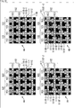
- the central pixel is arranged in the sub-block 103 unit, and normal pixels 111 are arranged at five locations on the top, bottom, left, and right, and functional pixels 111X at four other corners. May be arranged.
- the pixel 111 is arranged at the center pixel and the left and right diagonally upper and left and right diagonally lower 5 in the sub-block 103 unit.
- the functional pixel 111X may be arranged at a place.
- only the lower right pixel of the B sub-block 103 may be the black pixel 111C for the lower right pixel.
- the functional pixels 111X excluding the black pixel 111C in the sub-block 103 are arranged asymmetrically, but the normal pixels 111 in the sub-block 103 are arranged symmetrically in the vertical and horizontal directions. The occurrence of the phase shift is suppressed. Further, since the black pixels 111C are arranged uniformly, it is possible to appropriately correct a two-dimensional change in black level.
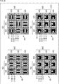
- phase difference detection pixels 111B-1 and 111B-2 are arranged on the left and right oblique upper sides as viewed from the center pixel in the sub-block 103 unit, and the left and right oblique lower parts.
- the black pixel 111C may be arranged, and the other five pixels may be the normal pixels 111.
- phase difference detection pixels 111B′-1 and 111B′-2 are arranged on the upper and lower diagonal portions on the right side when viewed from the center pixel.
- the black pixel 111C is arranged on the left diagonal upper and lower parts, and the other five pixels are set as normal pixels 111.
- the R and B sub-blocks 103 are diagonally upper left and right as viewed from the central pixel.
- the phase difference detection pixels 111B-1 and 111B-2 may be arranged, the black pixels 111C may be arranged at the lower left and right sides, and the other five pixels may be the normal pixels 111.
- the arrangement of the RGB sub-blocks 103 in the Bayer array of each block 102 corresponds to FIG.
- the central pixel 111 in the sub-block 103 may be replaced with a white pixel 111D with respect to the upper left pixel arrangement of FIG.
- the central pixel 111 in the sub-block 103 may be replaced with a white pixel 111D in the pixel arrangement in the lower left part of FIG.
- the normal pixels 111 are arranged symmetrically with respect to the top, bottom, left and right in the sub-block 103, so that the occurrence of phase shift can be suppressed.
- the sub-block 103 is configured by 9 pixels of 3 pixels ⁇ 3 pixels.
- the number of pixels constituting the sub-block 103 may be other number of pixels.
- it may be configured by 4 pixels ⁇ 4 pixels.
- the center 2 pixels ⁇ 2 pixels are phase difference detection pixels 111B-1 on the left and right respectively.
- 111B-2, and the normal pixels 111 may be arranged for the other 12 pixels.
- the center 2 pixels ⁇ 2 pixels of the G sub-block 103 are phase-detected left and right.
- the normal pixel 111 is arranged, and for the 2 pixels ⁇ 2 pixels at the center of the B and R sub-block 103, the left and right pixels 111B-1 and 111B-2 are arranged.
- phase difference detection pixels 111B′-1 and 111B′-2 may be arranged, and normal pixels 111 may be arranged for the other 12 pixels.
- the black pixel 111C may be arranged for the two pixels at the lower center stage, and the normal pixel 111 may be arranged for the other 12 pixels.
- the two pixels at the upper center of the G sub-block 103 are the phase difference detection pixels 111B- 1, 111B-2 are arranged, the black pixels 111C are arranged for the two pixels at the lower center stage, and the normal pixels 111 are arranged for the other 12 pixels, and the B and R sub-blocks 103 Phase difference detection pixels 111B′-1 and 111B′-2 are arranged for the two pixels on the left side of the center, black pixels 111C are arranged for the two pixels on the right side of the center, and the other 12 pixels are usually
- the pixels 111 may be arranged.
- sub-block 103 may be configured by 2 pixels ⁇ 2 pixels.
- phase difference detection pixels 111B-1 and 111B-2 are provided in the lower right portion, and the lower stage constituting the block 102
- a black pixel 111C may be provided at the lower right.
- 1 ⁇ 4 pixel is the functional pixel X.
- the functional pixel X may be not only the phase difference detection pixel 111B and the black pixel 111C shown in FIG. 33, but also the white pixel 111D and the single pixel 111A.
- the normal pixel 111 is asymmetric with respect to the upper, lower, left, and right in units of the subblock 103, but the arrangement of the three pixels 111 to be added is the same in all the subblocks 103. The deviation is suppressed. That is, as long as the arrangement of the pixels 111 used as the normal addition pixels is the same for each sub-block 103, the arrangement may be asymmetric regardless of the number of pixels constituting the sub-block 103.
- various functional pixels 111X may be arranged in various combinations at other positions.
- the electronic apparatus of the present disclosure in order to obtain information different from a normal image, even if any pixel in the pixel array is configured as a dedicated functional pixel for obtaining desired information, the captured image It is possible to suppress degradation of image quality.
- this indication can also take the following structures.
- the image picked up by the image pickup device is composed of blocks that are sets of color units, The block is configured by arranging, for each color, sub-blocks composed of a plurality of pixels of the same color in a predetermined color arrangement, Of the plurality of pixels arranged in the sub-block, the normal pixels are arranged symmetrically in the vertical and horizontal directions in the sub-block.
- ⁇ 2> The solid-state imaging device according to ⁇ 1>, wherein the color arrangement is a Bayer arrangement, a stripe arrangement, a checkered arrangement, or an interline arrangement.
- the pixel signals of the plurality of normal pixels constituting the sub-block are added and output as pixel signals of the normal addition pixels in the sub-block unit.
- ⁇ 4> The solid-state imaging device according to ⁇ 3>, wherein the functional pixel is a pixel having the same function as the normal pixel and captures the image having the same sensitivity and an exposure time different from that of the normal pixel. .
- the functional pixel is a pixel having the same function as that of the normal pixel, and images the image having the same exposure time as the normal pixel and having a different sensitivity. apparatus.
- the image sensor outputs a pixel signal of the normal pixel after outputting a signal indicating a phase difference detected by the functional pixel including the phase difference detection pixel. ⁇ 7> apparatus.
- ⁇ 8> a lens that adjusts a focal point of light incident on the image sensor; A lens control unit for controlling the focal length of the lens, The lens control unit calculates a defocus amount of the lens according to the phase difference detected by the phase difference detection pixel, and controls a focal length of the lens based on the defocus amount.
- ⁇ 7 > The solid-state imaging device described in>.
- ⁇ 9> The solid-state imaging device according to ⁇ 6>, wherein the phase difference detection pixel detects a phase difference in a horizontal direction.
- the phase difference detection pixel detects a phase difference in a vertical direction.
- the solid-state imaging device according to ⁇ 3>, wherein the functional pixel is a black pixel and outputs a black level.
- the black pixel is a pixel whose entire surface is shielded from light.
- the solid-state imaging device further including a clamp unit that subtracts and clamps the black level of the black pixel from a pixel signal of the normal addition pixel.
- the functional pixel is a white pixel and outputs a luminance signal.
- the solid-state imaging device wherein the white pixel is a pixel with a transparent color filter or a pixel without the color filter.
- an LPF unit that applies a LPF (Low Pass Filter) to the pixel signal of the normal addition pixel;
- An HPF unit that multiplies the luminance signal by HPF (High Pass Filter);
- the solid-state imaging device further including an output unit of the LPF unit and an adding unit that adds the output of the HPF unit.
- ⁇ 17> further includes a column AD conversion unit that performs analog-to-digital conversion of signals output from the pixels arranged in an array constituting the imaging device in units of rows,
- the image picked up by the image pickup device is composed of blocks that are sets of color units, The block is configured by arranging, for each color, sub-blocks composed of a plurality of pixels of the same color in a predetermined color arrangement, Among the arrangements of a plurality of pixels constituting the sub-block, the normal pixels are arranged symmetrically vertically and horizontally within the sub-block.
Landscapes
- Engineering & Computer Science (AREA)
- Multimedia (AREA)
- Signal Processing (AREA)
- Physics & Mathematics (AREA)
- General Physics & Mathematics (AREA)
- Optics & Photonics (AREA)
- Spectroscopy & Molecular Physics (AREA)
- Transforming Light Signals Into Electric Signals (AREA)
- Color Television Image Signal Generators (AREA)
- Solid State Image Pick-Up Elements (AREA)
Abstract
La présente invention concerne un dispositif de capture d'image à semi-conducteurs et un dispositif électronique qui permettent de supprimer la détérioration de la qualité d'image d'une image capturée même si, afin d'obtenir des informations différentes d'une image normale, tout pixel dans un réseau de pixels est conçu sous la forme d'un pixel fonctionnel permettant d'obtenir des informations souhaitées. Dans une pluralité de pixels constituant un sous-bloc en réseau de Bayer RVB constituant un bloc qui est un ensemble d'unités de couleur, des pixels normaux qui capturent des images normales sont placés selon une symétrie verticale de haut en bas et de gauche à droite à l'intérieur du sous-bloc, et des pixels fonctionnels permettant d'obtenir des informations souhaitées autres que destinées à capturer des images sont placés dans d'autres positions. La présente invention peut s'appliquer à des dispositifs de capture d'image à semi-conducteurs.
Priority Applications (6)
| Application Number | Priority Date | Filing Date | Title |
|---|---|---|---|
| JP2019514362A JP7099446B2 (ja) | 2017-04-25 | 2018-04-11 | 固体撮像装置および電子機器 |
| EP18790913.0A EP3618430B1 (fr) | 2017-04-25 | 2018-04-11 | Dispositif de capture d'image à semi-conducteurs et instrument électronique |
| US16/603,065 US11233957B2 (en) | 2017-04-25 | 2018-04-11 | Solid state image sensor and electronic equipment |
| EP22151852.5A EP4027640B1 (fr) | 2017-04-25 | 2018-04-11 | Capteur d'images à l'état solide et équipement électronique |
| US17/647,562 US11637975B2 (en) | 2017-04-25 | 2022-01-10 | Solid state image sensor and electronic equipment |
| US18/191,586 US12184999B2 (en) | 2017-04-25 | 2023-03-28 | Solid state image sensor and electronic equipment for improving image quality |
Applications Claiming Priority (2)
| Application Number | Priority Date | Filing Date | Title |
|---|---|---|---|
| JP2017-085906 | 2017-04-25 | ||
| JP2017085906 | 2017-04-25 |
Related Child Applications (2)
| Application Number | Title | Priority Date | Filing Date |
|---|---|---|---|
| US16/603,065 A-371-Of-International US11233957B2 (en) | 2017-04-25 | 2018-04-11 | Solid state image sensor and electronic equipment |
| US17/647,562 Continuation US11637975B2 (en) | 2017-04-25 | 2022-01-10 | Solid state image sensor and electronic equipment |
Publications (1)
| Publication Number | Publication Date |
|---|---|
| WO2018198766A1 true WO2018198766A1 (fr) | 2018-11-01 |
Family
ID=63919711
Family Applications (1)
| Application Number | Title | Priority Date | Filing Date |
|---|---|---|---|
| PCT/JP2018/015157 Ceased WO2018198766A1 (fr) | 2017-04-25 | 2018-04-11 | Dispositif de capture d'image à semi-conducteurs et instrument électronique |
Country Status (4)
| Country | Link |
|---|---|
| US (3) | US11233957B2 (fr) |
| EP (2) | EP4027640B1 (fr) |
| JP (1) | JP7099446B2 (fr) |
| WO (1) | WO2018198766A1 (fr) |
Cited By (5)
| Publication number | Priority date | Publication date | Assignee | Title |
|---|---|---|---|---|
| EP3674848A4 (fr) * | 2018-11-12 | 2020-10-21 | Shenzhen Goodix Technology Co., Ltd. | Appareil de détection optique et terminal |
| CN113875009A (zh) * | 2019-06-25 | 2021-12-31 | 索尼半导体解决方案公司 | 固态摄像装置和电子设备 |
| EP4035942A4 (fr) * | 2019-09-24 | 2022-11-30 | Sony Semiconductor Solutions Corporation | Dispositif d'imagerie |
| JPWO2023105916A1 (fr) * | 2021-12-08 | 2023-06-15 | ||
| WO2024084930A1 (fr) * | 2022-10-17 | 2024-04-25 | ソニーグループ株式会社 | Dispositif d'imagerie à semi-conducteurs, son procédé de commande, et équipement électronique |
Families Citing this family (10)
| Publication number | Priority date | Publication date | Assignee | Title |
|---|---|---|---|---|
| JP5999750B2 (ja) * | 2011-08-25 | 2016-09-28 | ソニー株式会社 | 撮像素子、撮像装置及び生体撮像装置 |
| WO2019073814A1 (fr) * | 2017-10-13 | 2019-04-18 | ソニー株式会社 | Dispositif de détection de foyer, procédé associé et programme |
| CN114793262B (zh) * | 2021-01-26 | 2024-06-14 | 华为技术有限公司 | 一种图像传感器、摄像头、电子设备及控制方法 |
| KR102890135B1 (ko) * | 2021-03-10 | 2025-11-21 | 삼성전자 주식회사 | 이미지 센서, 및 이미지 센서를 포함하는 카메라 모듈 |
| US11706537B2 (en) * | 2021-05-11 | 2023-07-18 | Omnivision Technologies, Inc. | Image sensor and method for reading out signal of image sensor |
| KR20240014226A (ko) | 2022-07-25 | 2024-02-01 | 삼성전자주식회사 | 위상 검출 픽셀을 포함하는 이미지 센서 |
| JP2025006152A (ja) * | 2023-06-29 | 2025-01-17 | キヤノン株式会社 | 光電変換装置、機器、および信号処理方法 |
| KR20250025879A (ko) * | 2023-08-16 | 2025-02-25 | 에스케이하이닉스 주식회사 | 빛 기반 연산을 수행하는 반도체 장치 및 반도체 장치의 동작 방법 |
| EP4528817B1 (fr) * | 2023-09-19 | 2026-01-14 | Gpixel NV | Pixel de mise au point automatique à détection de phase |
| CN120658944A (zh) * | 2024-03-14 | 2025-09-16 | 华为技术有限公司 | 一种图像拍摄方法与电子设备 |
Citations (4)
| Publication number | Priority date | Publication date | Assignee | Title |
|---|---|---|---|---|
| JP2013175898A (ja) * | 2012-02-24 | 2013-09-05 | Canon Inc | 撮像装置 |
| JP2014135564A (ja) * | 2013-01-08 | 2014-07-24 | Canon Inc | 撮像装置および画像処理装置 |
| JP2015133469A (ja) | 2013-12-12 | 2015-07-23 | ソニー株式会社 | 固体撮像素子およびその製造方法、並びに電子機器 |
| JP2016100879A (ja) * | 2014-11-26 | 2016-05-30 | オリンパス株式会社 | 撮像装置、画像処理方法 |
Family Cites Families (14)
| Publication number | Priority date | Publication date | Assignee | Title |
|---|---|---|---|---|
| JP5040458B2 (ja) * | 2007-06-16 | 2012-10-03 | 株式会社ニコン | 固体撮像素子及びこれを用いた撮像装置 |
| JP5233188B2 (ja) | 2007-07-11 | 2013-07-10 | 株式会社リコー | 画像形成装置 |
| JP5954964B2 (ja) | 2011-02-18 | 2016-07-20 | キヤノン株式会社 | 撮像装置およびその制御方法 |
| JP2013066146A (ja) * | 2011-08-31 | 2013-04-11 | Sony Corp | 画像処理装置、および画像処理方法、並びにプログラム |
| CN103782213B (zh) * | 2011-09-22 | 2015-11-25 | 富士胶片株式会社 | 数字相机 |
| EP2800379A4 (fr) * | 2011-12-27 | 2015-12-23 | Fujifilm Corp | Élément d'imagerie en couleurs |
| WO2014006784A1 (fr) | 2012-07-06 | 2014-01-09 | 富士フイルム株式会社 | Dispositif d'imagerie et procédé de traitement d'image |
| JP5787856B2 (ja) | 2012-09-24 | 2015-09-30 | 株式会社東芝 | 固体撮像装置 |
| WO2015049872A1 (fr) * | 2013-10-02 | 2015-04-09 | 株式会社ニコン | Élément de capture d'image et appareil de capture d'image |
| JP2017003832A (ja) * | 2015-06-12 | 2017-01-05 | キヤノン株式会社 | 自動焦点調節装置および光学機器 |
| KR102354991B1 (ko) * | 2017-05-24 | 2022-01-24 | 삼성전자주식회사 | 픽셀 회로 및 이를 포함하는 이미지 센서 |
| CN115720298B (zh) * | 2017-11-22 | 2025-05-30 | 索尼半导体解决方案公司 | 像素阵列、摄像元件和电子设备 |
| KR102545173B1 (ko) * | 2018-03-09 | 2023-06-19 | 삼성전자주식회사 | 위상 검출 픽셀들을 포함하는 이미지 센서 및 이미지 촬상 장치 |
| KR102684722B1 (ko) * | 2019-03-25 | 2024-07-12 | 삼성전자주식회사 | 이미지 센서 및 그 동작 방법 |
-
2018
- 2018-04-11 EP EP22151852.5A patent/EP4027640B1/fr active Active
- 2018-04-11 JP JP2019514362A patent/JP7099446B2/ja not_active Expired - Fee Related
- 2018-04-11 WO PCT/JP2018/015157 patent/WO2018198766A1/fr not_active Ceased
- 2018-04-11 US US16/603,065 patent/US11233957B2/en active Active
- 2018-04-11 EP EP18790913.0A patent/EP3618430B1/fr active Active
-
2022
- 2022-01-10 US US17/647,562 patent/US11637975B2/en active Active
-
2023
- 2023-03-28 US US18/191,586 patent/US12184999B2/en active Active
Patent Citations (4)
| Publication number | Priority date | Publication date | Assignee | Title |
|---|---|---|---|---|
| JP2013175898A (ja) * | 2012-02-24 | 2013-09-05 | Canon Inc | 撮像装置 |
| JP2014135564A (ja) * | 2013-01-08 | 2014-07-24 | Canon Inc | 撮像装置および画像処理装置 |
| JP2015133469A (ja) | 2013-12-12 | 2015-07-23 | ソニー株式会社 | 固体撮像素子およびその製造方法、並びに電子機器 |
| JP2016100879A (ja) * | 2014-11-26 | 2016-05-30 | オリンパス株式会社 | 撮像装置、画像処理方法 |
Non-Patent Citations (1)
| Title |
|---|
| See also references of EP3618430A4 |
Cited By (10)
| Publication number | Priority date | Publication date | Assignee | Title |
|---|---|---|---|---|
| EP3674848A4 (fr) * | 2018-11-12 | 2020-10-21 | Shenzhen Goodix Technology Co., Ltd. | Appareil de détection optique et terminal |
| CN113875009A (zh) * | 2019-06-25 | 2021-12-31 | 索尼半导体解决方案公司 | 固态摄像装置和电子设备 |
| EP3993400A4 (fr) * | 2019-06-25 | 2022-08-03 | Sony Semiconductor Solutions Corporation | Dispositif d'imagerie à semi-conducteurs et appareil électronique |
| US11843883B2 (en) | 2019-06-25 | 2023-12-12 | Sony Semiconductor Solutions Corporation | Solid-state imaging device and electronic device |
| TWI868161B (zh) * | 2019-06-25 | 2025-01-01 | 日商索尼半導體解決方案公司 | 固體攝像裝置及電子機器 |
| CN113875009B (zh) * | 2019-06-25 | 2025-11-21 | 索尼半导体解决方案公司 | 固态摄像装置和电子设备 |
| EP4035942A4 (fr) * | 2019-09-24 | 2022-11-30 | Sony Semiconductor Solutions Corporation | Dispositif d'imagerie |
| US11936979B2 (en) | 2019-09-24 | 2024-03-19 | Sony Semiconductor Solutions Corporation | Imaging device |
| JPWO2023105916A1 (fr) * | 2021-12-08 | 2023-06-15 | ||
| WO2024084930A1 (fr) * | 2022-10-17 | 2024-04-25 | ソニーグループ株式会社 | Dispositif d'imagerie à semi-conducteurs, son procédé de commande, et équipement électronique |
Also Published As
| Publication number | Publication date |
|---|---|
| EP3618430B1 (fr) | 2022-02-09 |
| US11637975B2 (en) | 2023-04-25 |
| JP7099446B2 (ja) | 2022-07-12 |
| EP4027640A1 (fr) | 2022-07-13 |
| US20220132058A1 (en) | 2022-04-28 |
| US20210105423A1 (en) | 2021-04-08 |
| JPWO2018198766A1 (ja) | 2020-02-27 |
| EP3618430A1 (fr) | 2020-03-04 |
| US20230239589A1 (en) | 2023-07-27 |
| EP3618430A4 (fr) | 2020-03-04 |
| EP4027640B1 (fr) | 2024-08-14 |
| US12184999B2 (en) | 2024-12-31 |
| US11233957B2 (en) | 2022-01-25 |
Similar Documents
| Publication | Publication Date | Title |
|---|---|---|
| JP7099446B2 (ja) | 固体撮像装置および電子機器 | |
| JP5319347B2 (ja) | 撮像装置及びその制御方法 | |
| US10015424B2 (en) | Method and apparatus for eliminating crosstalk amount included in an output signal | |
| US20110032395A1 (en) | Imaging unit and image sensor | |
| CN102025927B (zh) | 固态成像器件和电子装置 | |
| JP2009049525A (ja) | 撮像装置及び信号処理方法 | |
| JP2010147785A (ja) | 固体撮像素子及び撮像装置並びにその画像補正方法 | |
| US9813687B1 (en) | Image-capturing device, image-processing device, image-processing method, and image-processing program | |
| WO2021192176A1 (fr) | Dispositif de capture d'image | |
| JP5033711B2 (ja) | 撮像装置及び撮像装置の駆動方法 | |
| JP3965555B2 (ja) | 画像処理装置および方法、プログラム、並びに記録媒体 | |
| JP2015103971A (ja) | 固体撮像装置及びデジタルカメラ | |
| CN104025566A (zh) | 摄像装置、摄像装置的控制方法及控制程序 | |
| JP2008252397A (ja) | 撮像データの処理方法及び撮像装置 | |
| JP2003101815A (ja) | 信号処理装置及び信号処理方法 | |
| JP4279562B2 (ja) | 固体撮像装置の制御方法 | |
| WO2020049867A1 (fr) | Dispositif de capture d'image et élément de capture d'image | |
| JP2009303020A (ja) | 撮像装置及び欠陥画素補正方法 | |
| JP4645607B2 (ja) | 画像処理装置および方法、プログラム、並びに記録媒体 | |
| JP2009049524A (ja) | 撮像装置及び信号処理方法 | |
| JP2017208651A (ja) | 撮像装置 | |
| Zhang | Film-like images with super-fine details using Foveon X3 technology | |
| JP2015177257A (ja) | 固体撮像装置 | |
| JP2020048135A (ja) | 撮像装置及びその制御方法 | |
| JP5159387B2 (ja) | 撮像装置および撮像素子の駆動方法 |
Legal Events
| Date | Code | Title | Description |
|---|---|---|---|
| 121 | Ep: the epo has been informed by wipo that ep was designated in this application |
Ref document number: 18790913 Country of ref document: EP Kind code of ref document: A1 |
|
| ENP | Entry into the national phase |
Ref document number: 2019514362 Country of ref document: JP Kind code of ref document: A |
|
| NENP | Non-entry into the national phase |
Ref country code: DE |
|
| ENP | Entry into the national phase |
Ref document number: 2018790913 Country of ref document: EP Effective date: 20191125 |