WO2019013286A1 - Dispositif à semi-conducteur - Google Patents
Dispositif à semi-conducteur Download PDFInfo
- Publication number
- WO2019013286A1 WO2019013286A1 PCT/JP2018/026339 JP2018026339W WO2019013286A1 WO 2019013286 A1 WO2019013286 A1 WO 2019013286A1 JP 2018026339 W JP2018026339 W JP 2018026339W WO 2019013286 A1 WO2019013286 A1 WO 2019013286A1
- Authority
- WO
- WIPO (PCT)
- Prior art keywords
- region
- surface side
- lifetime control
- control region
- semiconductor device
- Prior art date
- Legal status (The legal status is an assumption and is not a legal conclusion. Google has not performed a legal analysis and makes no representation as to the accuracy of the status listed.)
- Ceased
Links
Images












Classifications
-
- H—ELECTRICITY
- H10—SEMICONDUCTOR DEVICES; ELECTRIC SOLID-STATE DEVICES NOT OTHERWISE PROVIDED FOR
- H10P—GENERIC PROCESSES OR APPARATUS FOR THE MANUFACTURE OR TREATMENT OF DEVICES COVERED BY CLASS H10
- H10P32/00—Diffusion of dopants within, into or out of wafers, substrates or parts of devices
- H10P32/10—Diffusion of dopants within, into or out of semiconductor bodies or layers
- H10P32/18—Diffusion lifetime killers
-
- H—ELECTRICITY
- H10—SEMICONDUCTOR DEVICES; ELECTRIC SOLID-STATE DEVICES NOT OTHERWISE PROVIDED FOR
- H10D—INORGANIC ELECTRIC SEMICONDUCTOR DEVICES
- H10D12/00—Bipolar devices controlled by the field effect, e.g. insulated-gate bipolar transistors [IGBT]
- H10D12/01—Manufacture or treatment
- H10D12/031—Manufacture or treatment of IGBTs
- H10D12/032—Manufacture or treatment of IGBTs of vertical IGBTs
- H10D12/038—Manufacture or treatment of IGBTs of vertical IGBTs having a recessed gate, e.g. trench-gate IGBTs
-
- H—ELECTRICITY
- H10—SEMICONDUCTOR DEVICES; ELECTRIC SOLID-STATE DEVICES NOT OTHERWISE PROVIDED FOR
- H10D—INORGANIC ELECTRIC SEMICONDUCTOR DEVICES
- H10D12/00—Bipolar devices controlled by the field effect, e.g. insulated-gate bipolar transistors [IGBT]
- H10D12/411—Insulated-gate bipolar transistors [IGBT]
- H10D12/441—Vertical IGBTs
- H10D12/461—Vertical IGBTs having non-planar surfaces, e.g. having trenches, recesses or pillars in the surfaces of the emitter, base or collector regions
- H10D12/481—Vertical IGBTs having non-planar surfaces, e.g. having trenches, recesses or pillars in the surfaces of the emitter, base or collector regions having gate structures on slanted surfaces, on vertical surfaces, or in grooves, e.g. trench gate IGBTs
-
- H—ELECTRICITY
- H10—SEMICONDUCTOR DEVICES; ELECTRIC SOLID-STATE DEVICES NOT OTHERWISE PROVIDED FOR
- H10D—INORGANIC ELECTRIC SEMICONDUCTOR DEVICES
- H10D30/00—Field-effect transistors [FET]
- H10D30/60—Insulated-gate field-effect transistors [IGFET]
-
- H—ELECTRICITY
- H10—SEMICONDUCTOR DEVICES; ELECTRIC SOLID-STATE DEVICES NOT OTHERWISE PROVIDED FOR
- H10D—INORGANIC ELECTRIC SEMICONDUCTOR DEVICES
- H10D62/00—Semiconductor bodies, or regions thereof, of devices having potential barriers
- H10D62/10—Shapes, relative sizes or dispositions of the regions of the semiconductor bodies; Shapes of the semiconductor bodies
-
- H—ELECTRICITY
- H10—SEMICONDUCTOR DEVICES; ELECTRIC SOLID-STATE DEVICES NOT OTHERWISE PROVIDED FOR
- H10D—INORGANIC ELECTRIC SEMICONDUCTOR DEVICES
- H10D62/00—Semiconductor bodies, or regions thereof, of devices having potential barriers
- H10D62/10—Shapes, relative sizes or dispositions of the regions of the semiconductor bodies; Shapes of the semiconductor bodies
- H10D62/102—Constructional design considerations for preventing surface leakage or controlling electric field concentration
- H10D62/112—Constructional design considerations for preventing surface leakage or controlling electric field concentration for preventing surface leakage due to surface inversion layers, e.g. by using channel stoppers
-
- H—ELECTRICITY
- H10—SEMICONDUCTOR DEVICES; ELECTRIC SOLID-STATE DEVICES NOT OTHERWISE PROVIDED FOR
- H10D—INORGANIC ELECTRIC SEMICONDUCTOR DEVICES
- H10D62/00—Semiconductor bodies, or regions thereof, of devices having potential barriers
- H10D62/10—Shapes, relative sizes or dispositions of the regions of the semiconductor bodies; Shapes of the semiconductor bodies
- H10D62/124—Shapes, relative sizes or dispositions of the regions of semiconductor bodies or of junctions between the regions
- H10D62/126—Top-view geometrical layouts of the regions or the junctions
- H10D62/127—Top-view geometrical layouts of the regions or the junctions of cellular field-effect devices, e.g. multicellular DMOS transistors or IGBTs
-
- H—ELECTRICITY
- H10—SEMICONDUCTOR DEVICES; ELECTRIC SOLID-STATE DEVICES NOT OTHERWISE PROVIDED FOR
- H10D—INORGANIC ELECTRIC SEMICONDUCTOR DEVICES
- H10D62/00—Semiconductor bodies, or regions thereof, of devices having potential barriers
- H10D62/10—Shapes, relative sizes or dispositions of the regions of the semiconductor bodies; Shapes of the semiconductor bodies
- H10D62/129—Cathode regions of diodes
-
- H—ELECTRICITY
- H10—SEMICONDUCTOR DEVICES; ELECTRIC SOLID-STATE DEVICES NOT OTHERWISE PROVIDED FOR
- H10D—INORGANIC ELECTRIC SEMICONDUCTOR DEVICES
- H10D62/00—Semiconductor bodies, or regions thereof, of devices having potential barriers
- H10D62/10—Shapes, relative sizes or dispositions of the regions of the semiconductor bodies; Shapes of the semiconductor bodies
- H10D62/13—Semiconductor regions connected to electrodes carrying current to be rectified, amplified or switched, e.g. source or drain regions
- H10D62/141—Anode or cathode regions of thyristors; Collector or emitter regions of gated bipolar-mode devices, e.g. of IGBTs
-
- H—ELECTRICITY
- H10—SEMICONDUCTOR DEVICES; ELECTRIC SOLID-STATE DEVICES NOT OTHERWISE PROVIDED FOR
- H10D—INORGANIC ELECTRIC SEMICONDUCTOR DEVICES
- H10D62/00—Semiconductor bodies, or regions thereof, of devices having potential barriers
- H10D62/10—Shapes, relative sizes or dispositions of the regions of the semiconductor bodies; Shapes of the semiconductor bodies
- H10D62/13—Semiconductor regions connected to electrodes carrying current to be rectified, amplified or switched, e.g. source or drain regions
- H10D62/141—Anode or cathode regions of thyristors; Collector or emitter regions of gated bipolar-mode devices, e.g. of IGBTs
- H10D62/142—Anode regions of thyristors or collector regions of gated bipolar-mode devices
-
- H—ELECTRICITY
- H10—SEMICONDUCTOR DEVICES; ELECTRIC SOLID-STATE DEVICES NOT OTHERWISE PROVIDED FOR
- H10D—INORGANIC ELECTRIC SEMICONDUCTOR DEVICES
- H10D62/00—Semiconductor bodies, or regions thereof, of devices having potential barriers
- H10D62/10—Shapes, relative sizes or dispositions of the regions of the semiconductor bodies; Shapes of the semiconductor bodies
- H10D62/17—Semiconductor regions connected to electrodes not carrying current to be rectified, amplified or switched, e.g. channel regions
- H10D62/393—Body regions of DMOS transistors or IGBTs
-
- H—ELECTRICITY
- H10—SEMICONDUCTOR DEVICES; ELECTRIC SOLID-STATE DEVICES NOT OTHERWISE PROVIDED FOR
- H10D—INORGANIC ELECTRIC SEMICONDUCTOR DEVICES
- H10D62/00—Semiconductor bodies, or regions thereof, of devices having potential barriers
- H10D62/50—Physical imperfections
- H10D62/53—Physical imperfections the imperfections being within the semiconductor body
-
- H—ELECTRICITY
- H10—SEMICONDUCTOR DEVICES; ELECTRIC SOLID-STATE DEVICES NOT OTHERWISE PROVIDED FOR
- H10D—INORGANIC ELECTRIC SEMICONDUCTOR DEVICES
- H10D62/00—Semiconductor bodies, or regions thereof, of devices having potential barriers
- H10D62/60—Impurity distributions or concentrations
-
- H—ELECTRICITY
- H10—SEMICONDUCTOR DEVICES; ELECTRIC SOLID-STATE DEVICES NOT OTHERWISE PROVIDED FOR
- H10D—INORGANIC ELECTRIC SEMICONDUCTOR DEVICES
- H10D64/00—Electrodes of devices having potential barriers
- H10D64/111—Field plates
-
- H—ELECTRICITY
- H10—SEMICONDUCTOR DEVICES; ELECTRIC SOLID-STATE DEVICES NOT OTHERWISE PROVIDED FOR
- H10D—INORGANIC ELECTRIC SEMICONDUCTOR DEVICES
- H10D8/00—Diodes
- H10D8/422—PN diodes having the PN junctions in mesas
-
- H—ELECTRICITY
- H10—SEMICONDUCTOR DEVICES; ELECTRIC SOLID-STATE DEVICES NOT OTHERWISE PROVIDED FOR
- H10D—INORGANIC ELECTRIC SEMICONDUCTOR DEVICES
- H10D84/00—Integrated devices formed in or on semiconductor substrates that comprise only semiconducting layers, e.g. on Si wafers or on GaAs-on-Si wafers
- H10D84/60—Integrated devices formed in or on semiconductor substrates that comprise only semiconducting layers, e.g. on Si wafers or on GaAs-on-Si wafers characterised by the integration of at least one component covered by groups H10D10/00 or H10D18/00, e.g. integration of BJTs
- H10D84/611—Combinations of BJTs and one or more of diodes, resistors or capacitors
- H10D84/613—Combinations of vertical BJTs and one or more of diodes, resistors or capacitors
- H10D84/617—Combinations of vertical BJTs and only diodes
-
- H—ELECTRICITY
- H10—SEMICONDUCTOR DEVICES; ELECTRIC SOLID-STATE DEVICES NOT OTHERWISE PROVIDED FOR
- H10D—INORGANIC ELECTRIC SEMICONDUCTOR DEVICES
- H10D84/00—Integrated devices formed in or on semiconductor substrates that comprise only semiconducting layers, e.g. on Si wafers or on GaAs-on-Si wafers
- H10D84/80—Integrated devices formed in or on semiconductor substrates that comprise only semiconducting layers, e.g. on Si wafers or on GaAs-on-Si wafers characterised by the integration of at least one component covered by groups H10D12/00 or H10D30/00, e.g. integration of IGFETs
- H10D84/811—Combinations of field-effect devices and one or more diodes, capacitors or resistors
-
- H—ELECTRICITY
- H10—SEMICONDUCTOR DEVICES; ELECTRIC SOLID-STATE DEVICES NOT OTHERWISE PROVIDED FOR
- H10P—GENERIC PROCESSES OR APPARATUS FOR THE MANUFACTURE OR TREATMENT OF DEVICES COVERED BY CLASS H10
- H10P32/00—Diffusion of dopants within, into or out of wafers, substrates or parts of devices
- H10P32/10—Diffusion of dopants within, into or out of semiconductor bodies or layers
- H10P32/17—Diffusion of dopants within, into or out of semiconductor bodies or layers characterised by the semiconductor material
- H10P32/171—Diffusion of dopants within, into or out of semiconductor bodies or layers characterised by the semiconductor material being group IV material
-
- H—ELECTRICITY
- H10—SEMICONDUCTOR DEVICES; ELECTRIC SOLID-STATE DEVICES NOT OTHERWISE PROVIDED FOR
- H10D—INORGANIC ELECTRIC SEMICONDUCTOR DEVICES
- H10D64/00—Electrodes of devices having potential barriers
- H10D64/111—Field plates
- H10D64/117—Recessed field plates, e.g. trench field plates or buried field plates
-
- H—ELECTRICITY
- H10—SEMICONDUCTOR DEVICES; ELECTRIC SOLID-STATE DEVICES NOT OTHERWISE PROVIDED FOR
- H10P—GENERIC PROCESSES OR APPARATUS FOR THE MANUFACTURE OR TREATMENT OF DEVICES COVERED BY CLASS H10
- H10P30/00—Ion implantation into wafers, substrates or parts of devices
- H10P30/20—Ion implantation into wafers, substrates or parts of devices into semiconductor materials, e.g. for doping
- H10P30/202—Ion implantation into wafers, substrates or parts of devices into semiconductor materials, e.g. for doping characterised by the semiconductor materials
- H10P30/204—Ion implantation into wafers, substrates or parts of devices into semiconductor materials, e.g. for doping characterised by the semiconductor materials into Group IV semiconductors
-
- H—ELECTRICITY
- H10—SEMICONDUCTOR DEVICES; ELECTRIC SOLID-STATE DEVICES NOT OTHERWISE PROVIDED FOR
- H10P—GENERIC PROCESSES OR APPARATUS FOR THE MANUFACTURE OR TREATMENT OF DEVICES COVERED BY CLASS H10
- H10P30/00—Ion implantation into wafers, substrates or parts of devices
- H10P30/20—Ion implantation into wafers, substrates or parts of devices into semiconductor materials, e.g. for doping
- H10P30/208—Ion implantation into wafers, substrates or parts of devices into semiconductor materials, e.g. for doping of electrically inactive species
Definitions
- the present invention relates to a semiconductor device.
- Patent Document 1 JP-A-2017-41601
- Patent Document 2 JP-A-2012-43891
- a semiconductor substrate having a drift region of a first conductivity type, a transistor part provided on the semiconductor substrate, and the semiconductor part provided on the semiconductor substrate and arranged along a predetermined arrangement direction And a diode unit arranged in the semiconductor device.
- Both the transistor part and the diode part may have a base region of the second conductivity type provided above the drift region inside the semiconductor substrate.
- Both the transistor portion and the diode portion penetrate the base region from the upper surface of the semiconductor substrate, extend in the extending direction perpendicular to the arrangement direction on the upper surface of the semiconductor substrate, and have a plurality of trench portions provided with the conductive portions therein.
- Both the transistor part and the diode part may be provided on the lower surface side of the semiconductor substrate from the transistor part to the diode part, and may have a lower surface side lifetime control region including a lifetime killer.
- the lower surface side lifetime control region may be provided in a part of the transistor portion in the arrangement direction and may not be provided in the other part.
- the lower surface side lifetime control region may be provided in a part of the diode section in the arrangement direction and not in another part.
- the diode portion is a cathode region of the first conductivity type exposed on the lower surface of the semiconductor substrate, and a floating region of the second conductivity type electrically floating provided on the lower surface side of the semiconductor substrate And may be included.
- the floating region may cover a portion of the cathode region above the cathode region.
- the floating region may be provided on the lower surface side of the semiconductor substrate than the lower surface side lifetime control region. In a top view of the semiconductor substrate, at least a part of the floating region may overlap the lower surface side lifetime control region.
- a plurality of floating regions may be provided in the arrangement direction. In the top view of the semiconductor substrate, at least one floating region of the plurality of floating regions may not overlap the lower surface side lifetime control region in the arrangement direction.
- the lower surface side lifetime control region may be provided in the entire diode section in the arrangement direction. In the arrangement direction, the length of the lower surface side lifetime control region in the transistor portion may be longer than the length of the lower surface side lifetime control region in the diode portion.
- the semiconductor device may further include an upper surface side lifetime control region provided on the upper surface side of the semiconductor substrate from the transistor portion to the diode portion and including a lifetime killer.
- the lower surface side lifetime control region may be provided closer to the diode portion in the arrangement direction than the upper surface side lifetime control region.
- the semiconductor device may further include a collector region provided on the lower surface of the semiconductor substrate.
- a collector region may be provided on the extension of the path from the end of the upper surface side lifetime control region in the transistor portion to the end of the lower surface side lifetime control region in the transistor portion in the arrangement direction.
- the lower surface side lifetime control region may be provided closer to the transistor portion in the arrangement direction than the upper surface side lifetime control region.
- the lifetime killer concentration of the lower surface side lifetime control region may be higher than the lifetime killer concentration of the upper surface side lifetime control region.
- the length of the upper surface side lifetime control region in the transistor portion may be not less than 0.01 times and not more than 0.15 times the length of the transistor portion.
- the distance in the direction parallel to the lower surface of the semiconductor substrate between the end of the upper surface side lifetime control region of the transistor portion and the end of the lower surface side lifetime control region of the transistor portion is the upper surface side of the transistor portion
- the length may be 0.25 times or more and 0.5 times or less the length of the lifetime control region.
- the lower surface side lifetime control region may be provided to the outside of the upper surface side lifetime control region in the stretching direction.
- the length of the upper surface side lifetime control region may be larger than the thickness of the semiconductor substrate.
- a plurality of lower surface side lifetime control regions may be provided in the depth direction of the semiconductor substrate.
- the lower surface side lifetime control region provided on the lower surface side of the semiconductor substrate is provided closer to the diode portion in the arrangement direction than the lower surface lifetime control region provided on the upper surface side of the semiconductor substrate. It may be done.
- a portion from the end of the lower surface side lifetime control region provided on the upper surface side of the semiconductor substrate to the end portion of the lower surface side lifetime control region provided on the lower surface side of the semiconductor substrate has a convex shape It may be located at
- the lower surface side lifetime control region provided on the lower surface side of the semiconductor substrate is provided closer to the diode portion in the arrangement direction than the lower surface lifetime control region provided on the upper surface side of the semiconductor substrate. It may be done.
- the lifetime killer concentration of the lower surface side lifetime control region provided on the lower surface side of the semiconductor substrate may be higher than the lifetime killer concentration of the lower surface side lifetime control region provided on the upper surface side of the semiconductor substrate.
- the length of the lower surface side lifetime control region in the diode portion may be not less than 0.015 times and not more than 0.03 times the length of the diode portion.
- the semiconductor device may further include a buffer region of the first conductivity type provided below the drift region, from the transistor portion to the diode portion.
- the lower surface side lifetime control area may be provided in the buffer area.
- the semiconductor device may further include a buffer region of the first conductivity type provided below the drift region, from the transistor portion to the diode portion.
- the thickness of the buffer area provided below the lower surface side lifetime control area may be larger than the thickness of the buffer area not provided below the lower surface side lifetime control area.
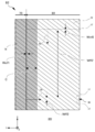
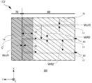
- FIG. 1 It is a figure which shows partially the upper surface of the semiconductor device 100 which concerns on embodiment of this invention. It is a figure which shows an example of the aa 'cross section in FIG. It is a figure which shows another example of the aa 'cross section in FIG. It is a figure which shows another example of the aa 'cross section in FIG. It is a figure which shows another example of the aa 'cross section in FIG. It is a figure which shows partially the upper surface of the semiconductor device 150 of a comparative example. It is a figure which shows an example of the aa-aa 'cross section in FIG. FIG.
- FIG. 7 is a view showing an example of lifetime killer concentration distributions of the upper surface side lifetime control region 72 and the lower surface side lifetime control region 74 in the bb ′ cross section of FIG. 2; It is a figure which shows another example of the aa 'cross section in FIG. It is a figure which shows another example of the aa 'cross section in FIG.
- FIG. 10 is a view showing an example of lifetime killer concentration distributions of the upper surface side lifetime control region 72 and the lower surface side lifetime control region 74-1 to the lower surface side lifetime control region 74-4 in the ff 'cross section of FIG. 9; It is a figure which shows an example of the semiconductor chip 98 which concerns on embodiment of this invention. It is an enlarged view of the area
- FIG. 13 is a view showing another example of the gg ′ cross section in FIG. 12;
- FIG. 13 is a view showing another example of the gg ′ cross section in FIG. 12;
- 17 is a view showing an example of lifetime killer concentration distribution in the Y-axis direction of the lower surface side lifetime control region 74-4 in the hh 'cross section of FIG. 15 and the jj' cross section of FIG. 16;
- It is a figure which shows partially the upper surface of the other semiconductor device 200 which concerns on this embodiment. It is an enlarged view of the area
- FIG. 19 is a view showing an example of a qq 'cross section in FIG. 18;
- FIG. 19 is a view showing an example of a qq 'cross section in FIG. 18;
- FIG. 19 is a view showing an example of a qq 'cross section in FIG. 18;
- FIG. 19 is a view showing an example of a qq 'cross section in FIG.
- FIG. 21 is a cross-sectional view taken along the line kk ′ in FIG. 20, including the transistor section 70 adjacent to the Y axis negative side of the diode section 80. It is a figure showing an example of the upper surface of semiconductor chip 120 concerning this embodiment. It is an enlarged view of area
- FIG. 24 is a view showing an example of a hh ′ cross section in FIG. 23; FIG. 24 is a view showing an example of a jj ′ cross section in FIG. 23; FIG. 23 is another enlarged view of a region A1 in FIG. 22.
- FIG. 29 is an enlarged view of a region C1 in FIG. 28.
- FIG. 30 is an enlarged view of a region C2 in FIG. 29. It is a figure which shows an example of the kk 'cross section in FIG.
- FIG. 29 is a view showing an example of the m-m 'cross section in FIG. 28.
- one side in a direction parallel to the depth direction of the semiconductor substrate is referred to as “upper”, and the other side is referred to as “lower”.
- the upper surface is referred to as the upper surface
- the other surface is referred to as the lower surface.
- the directions of “upper” and “lower” are not limited to the direction of gravity or the mounting direction to a substrate or the like at the time of mounting of the semiconductor device.
- the first conductivity type is N-type and the second conductivity type is P-type is shown, but the first conductivity type may be P-type and the second conductivity type may be N-type.
- the conductivity types of the substrate, layer, region and the like in the respective embodiments have opposite polarities.
- doping concentration refers to the concentration of donor or acceptor turned impurities.
- concentration difference between the donor and the acceptor may be referred to as the doping concentration.
- the peak value may be used as the doping concentration in the doping region.
- the average value of the doping concentrations in the doping region may be used as the doping concentration.
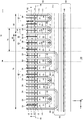
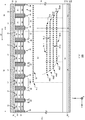
- FIG. 1 is a view partially showing an example of an upper surface of a semiconductor device 100 according to an embodiment of the present invention.
- the semiconductor device 100 of this example is a semiconductor chip provided with a transistor unit 70 and a diode unit 80.
- the transistor unit 70 includes a transistor such as an IGBT.
- the diode unit 80 includes a diode such as a free wheel diode (FWD) provided parallel to the transistor unit 70 on the upper surface of the semiconductor substrate.
- FWD free wheel diode
- a region located at the boundary between the transistor unit 70 and the diode unit 80 is a boundary unit 90.
- FIG. 1 the chip top surface around the chip end is shown, and other regions are omitted.
- FIG. 1 shows the active region of the semiconductor substrate in the semiconductor device 100
- the semiconductor device 100 may have an edge termination structure portion surrounding the active region.
- the active region indicates a region through which current flows when the semiconductor device 100 is controlled to be in an on state.
- the edge termination structure mitigates the concentration of the electric field on the upper surface side of the semiconductor substrate.
- the edge termination structure has, for example, a guard ring, a field plate, a resurf and a combination thereof.
- the semiconductor device 100 of this example is provided inside the semiconductor substrate, and the gate trench portion 40, the dummy trench portion 30, the well region 11, the emitter region 12, the base region 14 and the contact region 15 exposed on the upper surface of the semiconductor substrate. Equipped with, the semiconductor device 100 of this example includes the emitter electrode 52 and the gate metal layer 50 provided above the upper surface of the semiconductor substrate. Emitter electrode 52 and gate metal layer 50 are provided separately from each other.
- An interlayer insulating film is provided between the emitter electrode 52 and the gate metal layer 50 and the upper surface of the semiconductor substrate, but is omitted in FIG.
- the contact hole 56, the contact hole 49 and the contact hole 54 are provided to penetrate the interlayer insulating film.
- emitter electrode 52 is connected to the dummy conductive portion in dummy trench portion 30 through contact hole 56. Between the emitter electrode 52 and the dummy conductive portion, a connection portion 25 formed of a conductive material such as polysilicon doped with an impurity may be provided. An insulating film such as an oxide film is provided between the connection portion 25 and the upper surface of the semiconductor substrate.
- the gate metal layer 50 contacts the gate runner 48 through the contact hole 49.
- the gate runner 48 is formed of polysilicon doped with an impurity. Gate runner 48 is connected to the gate conductive portion in gate trench portion 40 on the upper surface of the semiconductor substrate. Gate runner 48 is not connected to the dummy conductive portion in dummy trench portion 30.
- the gate runner 48 in this example is provided from the lower side of the contact hole 49 to the tip of the gate trench portion 40.
- An insulating film such as an oxide film is provided between the gate runner 48 and the upper surface of the semiconductor substrate.
- the gate conductive portion is exposed on the upper surface of the semiconductor substrate.
- the gate trench portion 40 contacts the gate runner 48 at the exposed portion of the gate conductive portion.
- Emitter electrode 52 and gate metal layer 50 are formed of a material containing a metal.
- each electrode is formed of aluminum or aluminum-silicon alloy.
- Each electrode may have a barrier metal formed of titanium, a titanium compound, or the like below the region formed of aluminum or the like.
- Each electrode may have a plug formed of tungsten or the like in the contact hole.
- the one or more gate trench portions 40 and the one or more dummy trench portions 30 are arranged at predetermined intervals along a predetermined arrangement direction (in this example, the Y-axis direction).
- the gate trench portion 40 in this example is formed by two extending portions 39 extending in parallel with the upper surface of the semiconductor substrate and extending in the extending direction (in this example, the X-axis direction) perpendicular to the arrangement direction; May have a connecting portion 41 connecting the two.
- at least a portion of the connection portion 41 is provided in a curved shape.
- the dummy trench portion 30 in the present example may have a U-shape on the upper surface of the semiconductor substrate, similarly to the gate trench portion 40. That is, the dummy trench portion 30 in this example may have two extension portions 29 extending in the extension direction and a connection portion 31 connecting the two extension portions 29.
- Emitter electrode 52 is provided above gate trench portion 40, dummy trench portion 30, well region 11, emitter region 12, base region 14 and contact region 15.
- Well region 11 is of the second conductivity type.
- Well region 11 is provided in a predetermined range from the end of the active region on the side where gate metal layer 50 is provided.
- the diffusion depth of the well region 11 may be deeper than the depths of the gate trench portion 40 and the dummy trench portion 30.
- a partial region on the gate metal layer 50 side of the gate trench portion 40 and the dummy trench portion 30 is provided in the well region 11.
- the bottoms of the ends in the extending direction of the gate trench portion 40 and the dummy trench portion 30 may be covered with the well region 11.
- the contact holes 54 are provided above the contact region 15 and the emitter region 12, respectively.
- the contact hole 54 is provided above the base region 14. Neither contact hole 54 is disposed above the base region 14 and the well region 11 disposed at both ends in the X-axis direction.
- a mesa portion is provided in contact with each trench portion in the Y-axis direction in a direction parallel to the upper surface of the semiconductor substrate.
- the mesa portion may be a portion of the semiconductor substrate sandwiched between two adjacent trench portions, and may be a portion from the upper surface of the semiconductor substrate to the deepest bottom of each trench portion.
- the extension portion of each trench portion may be one trench portion. That is, the region between the two extending portions may be a mesa portion.
- a transistor mesa portion 60 is provided in contact with each trench portion.
- a boundary mesa portion 62 is provided in the boundary portion 90 in contact with each trench portion.
- the diode mesa portion 64 is provided in a region sandwiched by the adjacent dummy trench portions 30.
- Base regions 14 are provided, as an example, at both ends of the transistor mesa 60, the boundary mesa 62, and the diode mesa 64 in the X-axis direction. In FIG. 1, only the base region 14 provided at one end in the X-axis direction is shown.
- Emitter region 12 is provided on the upper surface of transistor mesa 60 in contact with gate trench portion 40.
- the emitter region 12 of this example is of the first conductivity type.
- a contact region 15 of the second conductivity type which has a doping concentration higher than that of the base region 14, is provided.
- the emitter regions 12 and the contact regions 15 may be alternately provided in the extending direction of the gate trench portion 40.
- the emitter region 12 and the contact region 15 are provided also below the contact hole 54.
- Emitter region 12 may be provided in contact with dummy trench portion 30 on the upper surface of transistor mesa portion 60 or may be provided separately. Emitter region 12 in the example of FIG. 1 is provided in contact with dummy trench portion 30.
- a contact region 15 of the second conductivity type having a doping concentration higher than that of the base region 14 is provided on the top surface of the boundary mesa portion 62.
- the contact regions 15 may be provided in the entire region sandwiched by the base regions 14 provided at both ends of the boundary mesa portion 62 in the X-axis direction. In the boundary mesa portion 62, the contact region 15 is also provided below the contact hole 54.
- Contact regions 15 are provided on the top surface of the diode mesa 64 at both ends in the X-axis direction.
- a base region 14 is provided in a region sandwiched by the contact regions 15.
- the base region 14 may be provided in the entire region sandwiched by the contact regions 15.
- the base region 14 and the contact region 15 are also provided below the contact hole 54.
- the dummy trench portion 30 is provided in the diode portion 80.
- the linear extension portions 29 of the respective dummy trench portions 30 are connected by the connection portion 31.
- a diode mesa portion 64 is provided in a region sandwiched by the respective dummy trench portions 30.
- the emitter region 12 may not be provided in the diode mesa portion 64, and may be provided. In this example, the emitter region 12 is not provided.
- the contact region 15 or the base region 14 is provided from one dummy trench portion 30 sandwiching the diode mesa portion 64 to the other dummy trench portion 30. That is, on the upper surface of the semiconductor substrate, the width of the diode mesa 64 in the Y-axis direction is equal to the width of the contact region 15 or the base region 14 provided in the diode mesa 64 in the Y-axis direction.
- the diode section 80 has a cathode region 82 of the first conductivity type on the lower surface side of the semiconductor substrate.
- a region where the cathode region 82 is provided in a top view of the semiconductor substrate is indicated by a dashed-dotted line portion.
- the diode section 80 may be an area where the cathode area 82 is projected on the upper surface of the semiconductor substrate.
- the region where the cathode region 82 is projected on the upper surface of the semiconductor substrate may be separated from the contact region 15 in the + X axis direction.
- a collector region of the second conductivity type may be provided in a region exposed to the lower surface of the semiconductor substrate and not provided with the cathode region 82.
- the transistor portion 70 may be a region in which a trench portion or a mesa portion is provided in a region obtained by projecting the collector region on the upper surface of the semiconductor substrate.
- the upper surface side lifetime control region 72 including the lifetime killer is provided locally in the depth direction of the semiconductor substrate.
- a region where the upper surface side lifetime control region 72 is provided in a top view of the semiconductor substrate is indicated by a broken line portion.
- the upper surface side lifetime control area 72 is provided up to the area not shown in FIG. 1 of the area on the Y axis negative side and the areas on the X axis positive side and the negative side in FIG.
- a direction perpendicular to the semiconductor substrate in a top view of the semiconductor substrate is referred to as a depth direction (Z-axis direction).
- the lower surface side lifetime control region 74 including the lifetime killer is locally provided below the upper surface side lifetime control region 72 in the depth direction of the semiconductor substrate.
- a region where the lower surface side lifetime control region 74 is provided in a top view of the semiconductor substrate is indicated by a broken line portion.
- the lower surface side lifetime control area 74 is provided up to the area not shown in FIG. 1 of the areas on the X axis positive side and the negative side in FIG. 1.
- the range in which the upper surface side lifetime control area 72 is provided in the Y-axis direction may be wider than the area in which the lower surface side lifetime control area 74 is provided.
- the entire trench portion in the region where the upper surface side lifetime control region 72 is provided may be the dummy trench portion 30 in top view.
- the particle beam may be irradiated from the upper surface side to form the upper surface side lifetime control area 72.
- the gate insulating film may be damaged.
- the trench portion in the upper surface side lifetime control region 72 as the dummy trench portion 30, the occurrence of damage to the gate insulating film can be suppressed. Therefore, gate threshold fluctuation of the transistor and gate insulating film breakdown can be prevented.
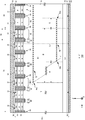
- FIG. 2 is a view showing an example of an aa ′ cross section in FIG.
- the aa ′ cross section is a YZ plane passing through the emitter region 12, the contact region 15 and the base region 14 in the transistor portion 70 and the diode portion 80.
- the semiconductor device 100 of this example has the semiconductor substrate 10, the interlayer insulating film 38, the emitter electrode 52, and the collector electrode 24 in the cross section aa '.
- Emitter electrode 52 is provided on upper surface 21 of semiconductor substrate 10 and the upper surface of interlayer insulating film 38.
- the collector electrode 24 is provided on the lower surface 23 of the semiconductor substrate 10. Emitter electrode 52 and collector electrode 24 are formed of a conductive material such as metal.
- the semiconductor substrate 10 may be a silicon substrate, a silicon carbide substrate, or a nitride semiconductor substrate such as gallium nitride.
- the semiconductor substrate 10 of this example is a silicon substrate.
- the semiconductor substrate 10 of this example includes the drift region 18 of the first conductivity type.
- the drift region 18 in this example is N + type.
- Drift region 18 may be a region remaining in semiconductor substrate 10 without forming another doping region. That is, the doping concentration of the drift region 18 may be the doping concentration of the semiconductor substrate 10.
- a buffer region 20 of the first conductivity type may be provided below the drift region 18.
- the doping concentration of buffer region 20 is higher than the doping concentration of drift region 18.
- Buffer region 20 may function as a field stop layer that prevents a depletion layer extending from the lower surface side of base region 14 from reaching collector region 22 and cathode region 82 of the second conductivity type.
- the diode portion 80 has a cathode region 82 below the buffer region 20.
- the cathode region 82 may be provided at the same depth as the collector region 22 of the transistor unit 70.
- the diode unit 80 may function as a free wheeling diode (FWD) that allows a return current to flow in the reverse direction when the transistor unit 70 of another semiconductor device 100 is turned off in a power conversion circuit such as an inverter.
- FWD free wheeling diode
- a collector region 22 of the second conductivity type is provided below the buffer region 20.
- the collector region 22 may extend to a region on the lower surface 23 side of the boundary mesa portion 62.
- the semiconductor device 100 of this example since the collector region 22 extends to the lower surface 23 of the boundary mesa portion 62, the distance between the emitter region 12 of the transistor portion 70 and the cathode region 82 of the diode portion 80 can be secured. Therefore, the semiconductor device 100 of this example can prevent the electrons injected from the gate structure including the emitter region 12 of the transistor unit 70 into the drift region 18 from flowing out into the cathode region 82 of the diode unit 80. .
- the distance between the contact region 15 of the boundary mesa portion 62 and the cathode region 82 of the diode portion 80 can also be longer than in the case where the cathode region 82 is provided immediately below the boundary mesa portion 62. Therefore, the semiconductor device 100 of this example can suppress the injection of holes from the contact region 15 having a doping concentration higher than that of the base region 14 to the cathode region 82 when the diode unit 80 conducts.
- the storage region 16 of the first conductivity type may be provided above the drift region 18.
- the accumulation region 16 is a region where the same dopant as the drift region 18 is accumulated at a higher concentration than the drift region 18.
- the doping concentration of storage region 16 is higher than the doping concentration of drift region 18.
- Storage region 16 is provided in contact with gate trench portion 40.
- a base region 14 of the second conductivity type is provided above the storage region 16 in the transistor mesa 60 and the boundary mesa 62.
- Base region 14 is provided in contact with gate trench portion 40.
- the emitter region 12 is provided between the base region 14 and the top surface 21 in the transistor mesa 60.
- Emitter region 12 is provided in contact with gate trench portion 40.
- the doping concentration of the emitter region 12 is higher than the doping concentration of the drift region 18.
- An example of the dopant of the emitter region 12 is arsenic (As).
- the contact region 15 of the second conductivity type is provided above the storage region 16 in the boundary mesa 62.
- Contact region 15 is provided in contact with gate trench portion 40.
- the emitter region 12 may not be provided.
- a storage region 16 is provided above the drift region 18 in the diode mesa 64. Further, in the present example, a base region 14 is provided above the storage region 16 in the diode mesa 64. Emitter region 12 may not be provided in diode mesa portion 64.
- the upper surface 21 is provided with one or more gate trench portions 40 and one or more dummy trench portions 30.
- Each trench portion is provided from the upper surface 21 to the drift region 18. In a region where at least one of emitter region 12, contact region 15 and storage region 16 is provided, each trench portion is also provided to penetrate drift region 18 to reach drift region 18.
- the fact that the trench portion penetrates the doping region is not limited to the one manufactured in the order of forming the doping region and then forming the trench portion. After forming the trench portion, those in which the doping region is formed between the trench portions are also included in those in which the trench portion penetrates the doping region.
- the gate trench portion 40 has a gate trench provided on the upper surface 21, a gate insulating film 42, and a gate conductive portion 44.
- the gate insulating film 42 is provided to cover the inner wall of the gate trench.
- the gate insulating film 42 may be formed by oxidizing or nitriding the semiconductor on the inner wall of the gate trench.
- the gate conductive portion 44 is provided inside the gate insulating film 42 inside the gate trench.
- the gate insulating film 42 insulates the gate conductive portion 44 and the semiconductor substrate 10.
- the gate conductive portion 44 is formed of a conductive material such as polysilicon.
- Gate trench portion 40 is covered with interlayer insulating film 38 on upper surface 21.
- the gate conductive portion 44 includes a region facing the base region 14 adjacent to the transistor mesa portion 60 with the gate insulating film 42 interposed therebetween. When a predetermined voltage is applied to the gate conductive portion 44, a channel of the inversion layer of electrons is formed in the surface layer of the interface in the base region 14 in contact with the gate trench.
- the dummy trench portion 30 may have the same structure as the gate trench portion 40 in FIG.
- the dummy trench portion 30 has a dummy trench, a dummy insulating film 32 and a dummy conductive portion 34 provided on the upper surface 21 side.
- the dummy insulating film 32 is provided to cover the inner wall of the dummy trench.
- the dummy conductive portion 34 is provided inside the dummy trench, and is provided inside the dummy insulating film 32.
- the dummy insulating film 32 insulates the dummy conductive portion 34 and the semiconductor substrate 10.
- the dummy trench portion 30 is covered with the interlayer insulating film 38 on the upper surface 21.
- the semiconductor device 100 of the present example has a lower surface side lifetime control region 74 provided on the lower surface 23 side of the semiconductor substrate 10 from the transistor unit 70 to the diode unit 80.
- the peak position in the Z-axis direction of the lifetime killer concentration distribution of the lower surface side lifetime control region 74 is indicated by a symbol “x”.
- one lower surface side lifetime control area 74 is provided in the Z-axis direction.
- the lower surface side lifetime control region 74 is provided in a part of the transistor unit 70 in the Y-axis direction, and is not provided in the other part of the transistor unit 70.
- the lower surface side lifetime control region 74 is provided in a part of the diode unit 80 in the Y-axis direction, and is not provided in the other part of the diode unit 80.
- T be the thickness of the semiconductor substrate 10.
- the lower surface side lifetime control region 74 is provided at a position deeper than half of the thickness T with reference to the upper surface 21.
- the leak current of the transistor section 70 tends to increase. Therefore, in the present embodiment, the lower surface side lifetime control region 74 is provided at a position shallower than half of the thickness T with reference to the upper surface 21.
- the semiconductor device 100 of this example has an upper surface side lifetime control region 72 provided on the upper surface 21 side of the semiconductor substrate 10 from the transistor unit 70 to the diode unit 80.
- the peak position in the Z-axis direction of the lifetime killer concentration distribution of the upper surface side lifetime control region 72 is indicated by a symbol “x”.
- the upper surface side lifetime control area 72 is provided on the entire diode section 80 in the Y-axis direction.
- the upper surface side lifetime control region 72 is provided up to the transistor portion 70 (not shown in FIG. 2) adjacent on the Y axis negative side of the diode portion 80.
- the lower surface side lifetime control region 74 in the transistor section 70 is provided on the Y axis negative side with respect to the upper surface side lifetime control region 72. That is, the end Klb of the lower surface side lifetime control area 74 in the transistor section 70 is located on the Y axis negative side with respect to the end Kls of the upper surface side lifetime control area 72.
- the upper surface side lifetime control region 72 and the lower surface side lifetime control region 74 are provided locally in the depth direction of the semiconductor substrate 10. That is, the defect density of the upper surface side lifetime control region 72 and the lower surface side lifetime control region 74 is higher than that of the other regions of the semiconductor substrate 10.
- An example of a lifetime killer is helium injected at a predetermined depth position. By injecting helium, crystal defects can be formed inside the semiconductor substrate 10.
- the lower surface side lifetime control region 74 has a function of improving the leak current characteristic caused by the upper surface side lifetime control region 72.
- the provision of the lower surface side lifetime control region 74 makes it easier for the minority carrier holes generated in the drift region 18 to be offset with the majority carrier electrons with a short lifetime. Therefore, the semiconductor device 100 of this example can improve the leakage current characteristics of the transistor section 70. Further, in the semiconductor device 100 of the present example, since the lower surface side lifetime control region 74 is provided, the trade-off between the on voltage of the transistor unit 70 and the turn off loss can be made favorable.
- the distance A is a distance in the Y-axis direction between the end Kls and the end Klb.
- the distance B is a distance from the end Kls to the boundary between the transistor unit 70 and the diode unit 80 in the Y-axis direction.
- the distance A may be smaller than the distance B.
- the distance A may be not less than 0.25 times and not more than 0.5 times the distance B.
- the distance A may be 50 ⁇ m to 100 ⁇ m.
- the lower surface side lifetime control region 74 is provided on the Y axis negative side of the upper surface side lifetime control region 72 in the transistor section 70. Therefore, the semiconductor device 100 of this example can suppress the injection of holes from the emitter region 12 of the transistor unit 70 to the cathode region 82 of the diode unit 80 when the diode unit 80 operates. Therefore, the semiconductor device 100 of this example can improve the reverse recovery characteristic of the diode unit 80.
- the length Lb is the length in the Y-axis direction of the lower surface side lifetime control area 74 in the transistor section 70.
- the length C is the length in the Y-axis direction of the lower surface side lifetime control area 74 in the diode section 80.
- the length Lb may be longer than the length C.
- the semiconductor device 100 of this example since the length Lb is longer than the length C, injection of holes from the emitter region 12 of the transistor unit 70 to the cathode region 82 of the diode unit 80 is suppressed when the diode unit 80 operates. it can. Therefore, the semiconductor device 100 of this example can improve the reverse recovery characteristic of the diode unit 80.
- the collector region 22 may be provided on an extension of the path from the end Kls to the end Klb, as indicated by the line rr ′ in FIG. That is, a straight line connecting the end Kls and the end Klb may intersect the collector region 22.
- a straight line connecting the end Kls and the end Klb is arranged to cross the collector region 22 so that holes moving from the emitter region 12 of the transistor to the cathode region 82 of the diode section 80 have a lifetime control on the lower surface side.
- the presence of the region 74 makes it easy to offset the electrons. Therefore, the semiconductor device 100 of this example can suppress the injection of holes from the emitter region 12 of the transistor unit 70 to the cathode region 82 of the diode unit 80 when the diode unit 80 operates.
- the lower surface side lifetime control region 74 in the diode section 80 is provided on the Y axis positive side with respect to the upper surface side lifetime control region 72. That is, in the present embodiment, the upper surface side lifetime control region 72 in the diode unit 80 is also provided on the Y axis negative side with respect to the end portion Krb of the lower surface side lifetime control region 74.
- FIG. 3 is a view showing another example of the aa ′ cross section in FIG.
- the semiconductor device 100 of FIG. 3 is different from the semiconductor device 100 of FIG. 2 in that the lower surface side lifetime control region 74 of the transistor section 70 is provided extending to the Y axis positive side with respect to the upper surface side lifetime control region 72. It is different.
- FIG. 3 shows an example in which the end Klb is disposed at a distance of A ′ on the Y axis positive side with respect to the end Kls.
- the lower surface side lifetime control region 74 of the transistor unit 70 is provided on the Y axis positive side with respect to the upper surface side lifetime control region 72. Therefore, the holes moving from the emitter region 12 of the transistor unit 70 to the cathode region 82 of the diode unit 80 are easily offset with the electrons due to the presence of the lower surface side lifetime control region 74. Therefore, the semiconductor device 100 of this example can suppress the injection of holes from the emitter region 12 of the transistor unit 70 to the cathode region 82 of the diode unit 80 when the diode unit 80 operates. Further, in the semiconductor device 100 of the present example, the leakage current characteristics of the transistor unit 70 can be improved by the presence of the lower surface side lifetime control region 74. Further, in the semiconductor device 100 of this example, the presence of the lower surface side lifetime control region 74 makes it possible to make good trade-off between the on voltage of the transistor section 70 and the turn off loss.
- FIG. 4 is a view showing another example of the aa ′ cross section in FIG.
- the semiconductor device 100 of FIG. 4 differs from the semiconductor device 100 of FIG. 2 in that the lower surface side lifetime control region 74 is provided in the buffer region 20.
- the lower surface side lifetime control region 74 is provided on the Y axis negative side with respect to the upper surface side lifetime control region 72. Therefore, the semiconductor device 100 of this example can suppress the injection of holes from the emitter region 12 of the transistor unit 70 to the cathode region 82 of the diode unit 80 when the diode unit 80 operates. Therefore, the semiconductor device 100 of this example can improve the reverse recovery characteristic of the diode unit 80. Further, in the semiconductor device 100 of the present example, since the lower surface side lifetime control region 74 is provided, the leak current characteristics of the transistor unit 70 can be improved. Further, in the semiconductor device 100 of the present example, since the lower surface side lifetime control region 74 is provided, the trade-off between the on voltage of the transistor unit 70 and the turn off loss can be made favorable.
- FIG. 5 is a view showing another example of the aa ′ cross section in FIG.
- the thickness Dk is the thickness in the Z-axis direction of the buffer region 20 in which the lower surface side lifetime control region 74 is provided on the upper side.
- the thickness D is the thickness in the Z-axis direction of the buffer area 20 where the lower surface side lifetime control area 74 is not provided at the upper side.
- the semiconductor device 100 of this example differs from the semiconductor device 100 of FIG. 2 in that the thickness Dk is larger than the thickness D.
- the lower surface side lifetime control region 74 is provided on the Y axis negative side with respect to the upper surface side lifetime control region 72. Therefore, the semiconductor device 100 of this example can suppress the injection of holes from the emitter region 12 of the transistor unit 70 to the cathode region 82 of the diode unit 80 when the diode unit 80 operates. Therefore, the semiconductor device 100 of this example can improve the reverse recovery characteristic of the diode unit 80. Further, in the semiconductor device 100 of the present example, since the lower surface side lifetime control region 74 is provided, the leak current characteristics of the transistor unit 70 can be improved. Further, in the semiconductor device 100 of the present example, since the lower surface side lifetime control region 74 is provided, the trade-off between the on voltage of the transistor unit 70 and the turn off loss can be made favorable.
- FIG. 6 is a view partially showing the upper surface of the semiconductor device 150 of the comparative example.
- the lower surface side lifetime control region 274 is provided over the entire transistor portion 70 and the diode portion 80 in the Y-axis direction.
- the upper surface side lifetime control region 72 is provided at the same position as that in FIG. 1 in a top view of the semiconductor substrate 10.
- the lower surface side lifetime control region 274 is provided up to regions on the Y axis positive side and negative side not shown in FIG.
- FIG. 7 is a view showing an example of the zz ′ cross section in FIG.
- the lower surface side lifetime control region 274 is provided below the upper surface side lifetime control region 272 over the entire transistor portion 70 and the diode portion 80 in the Y axis direction. .
- the trade-off between the on voltage of the transistor unit 70 and the turn-off loss is likely to deteriorate.
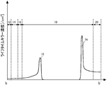
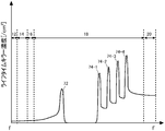
- FIG. 8 is a diagram showing an example of lifetime killer density distribution of the upper surface side lifetime control region 72 and the lower surface side lifetime control region 74 along the line bb ′ of FIG.
- helium ions are implanted from the upper surface 21 to form the upper surface side lifetime control region 72
- helium ions are implanted from the lower surface 23 to form the lower surface side lifetime control region 74.
- An example of the distribution is shown.
- the peak position (the depth in the Z-axis direction from the top surface 21) of the lifetime killer concentration of the top-side lifetime control area 72 is the Z-axis direction of the symbol “x” indicating the top-side lifetime control area 72 in FIG. Equal to the position in When helium ions are implanted from the upper surface 21, a lifetime killer having a concentration lower than the peak concentration may be distributed on the upper surface 21 side of the peak position.
- the peak position (the depth in the Z-axis direction from the lower surface 23) of the lifetime killer concentration of the lower surface-side lifetime control area 74 is the Z-axis direction of the symbol “x” indicating the lower surface side lifetime control area 74 in FIG. Equal to the position in When helium ions are implanted from the lower surface 23, a lifetime killer having a concentration lower than the peak concentration may be distributed closer to the lower surface 23 than the peak position.
- the peak concentration of the lifetime killer concentration of the lower surface side lifetime control region 74 may be higher or lower than the peak concentration of the lifetime killer concentration of the upper surface side lifetime control region 72.
- the peak concentration of the lifetime killer concentration of the lower surface side lifetime control region 74 is higher than the peak concentration of the lifetime killer concentration of the upper surface side lifetime control region 72.
- the lifetime killer concentration of the lower surface side lifetime control region 74 may be two to five times higher than the lifetime killer concentration of the upper surface side lifetime control region 72.
- the ordinate of the lifetime killer concentration distribution may be helium concentration, or may be the density of crystal defects formed by implantation of helium ions.
- the crystal defects may be interstitial helium, vacancies, double vacancies, and the like. These crystal defects form carrier recombination centers. Carrier recombination is promoted via the energy level (trap level) of the formed recombination center.
- the lifetime killer concentration corresponds to the trap level density.
- the lifetime killer concentration of the lower surface side lifetime control region 74 is higher than the lifetime killer concentration of the upper surface side lifetime control region 72. Therefore, in the semiconductor device 100 of this example, the carrier lifetime of the upper surface side lifetime control region 72 can be extended. Therefore, the semiconductor device 100 of this example can improve the leak current characteristic caused by the lifetime killer. Further, in the semiconductor device 100 of this example, the trade-off between the on voltage and the turn off loss of the transistor unit 70 can be made favorable.
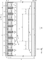
- FIG. 9 is a view showing another example of the aa ′ cross section in FIG.
- the semiconductor device 100 of FIG. 9 differs from the semiconductor device 100 of FIG. 2 in that a plurality of lower surface side lifetime control regions 74 are provided in the Z-axis direction.
- the semiconductor device 100 of FIG. 9 shows an example in which four lower surface side lifetime control regions 74 are provided in the Z-axis direction.
- the peak positions in the Z-axis direction of the lifetime killer concentration distribution of the lower surface side lifetime control region 74-1 to the lower surface side lifetime control region 74-4 are indicated by the symbol “x”.
- the lower surface side lifetime control area 74-4 provided on the lower surface 23 side is provided on the Y axis negative side than the lower surface side lifetime control area 74-1 provided on the upper surface 21 side. That is, as indicated by a broken line t-t 'in FIG. 9, the end of the lower surface side lifetime control area 74 is the end surface Klb1 of the lower surface side lifetime control area 74-1 to the lower surface side lifetime control area 74-4. It may be disposed on the Y axis negative side of FIG. The end Klb1 to the end Klb4 may be arranged in a straight line indicated by a broken line t-t 'in the YZ plane.
- the lower surface side lifetime control region 74-4 is provided on the Y axis negative side with respect to the upper surface side lifetime control region 72. Therefore, the semiconductor device 100 of this example can suppress the injection of holes from the emitter region 12 of the transistor unit 70 to the cathode region 82 of the diode unit 80 when the diode unit 80 operates. Therefore, the semiconductor device 100 of this example can improve the reverse recovery characteristic of the diode unit 80.
- the lengths in the Y-axis direction of the four lower surface side lifetime control areas 74 may be different from each other.
- the lower surface side lifetime control region 74-4 provided on the lower surface 23 side is provided on the Y axis negative side than the lower surface side lifetime control region 74-1 provided on the upper surface 21 side.
- the end of the lower surface side lifetime control region 74 is the lower surface side lifetime control region 74-4 from the end portion Krb1 of the lower surface side lifetime control region 74-1. It may be located on the Y axis negative side of FIG.
- the end Krb1 to the end Krb4 may be arranged in a straight line indicated by a broken line u-u 'in the YZ plane.
- the end on the Y-axis positive side of the lower surface side lifetime control region 74 is positioned on the Y-axis negative side as it extends from the end Klb1 to the end Klb4.
- the semiconductor device 100 of this example can suppress the injection of holes from the emitter region 12 of the transistor unit 70 to the cathode region 82 of the diode unit 80 when the diode unit 80 is operating.
- FIG. 10 is a view showing another example of the aa ′ cross section in FIG.
- the end Klb1 to the end Klb4 are arranged in a convex shape on the Y axis positive side in the YZ plane, This differs from the semiconductor device 100 of FIG.
- the end Klb2 and the end Klb3 are located on the positive side in the Y-axis direction.
- the end portion Krb1 to the end portion Krb4 are linearly arranged in the YZ plane, but may be arranged to be convex on the Y axis negative side, the Y axis positive side It may be arranged to have a convex shape.
- FIG. 11 shows the lifetime killer concentration distribution of the upper surface side lifetime control region 72 and the lower surface side lifetime control region 74-1 to the lower surface side lifetime control region 74-4 along the ff 'line of FIG. FIG.
- helium ions are injected from the lower surface 23, and an example of lifetime killer concentration distribution in the case where the lower surface side lifetime control region 74-1 to the lower surface side lifetime control region 74-4 are respectively formed is shown. ing.
- the peak position (the depth in the Z-axis direction from the lower surface 23) of the lifetime killer concentration of the lower surface-side lifetime control area 74 is the Z-axis direction of the symbol “x” indicating the lower surface side lifetime control area 74 in FIG. Equal to the position in When helium ions are implanted from the lower surface 23, a lifetime killer having a concentration lower than the peak concentration may be distributed closer to the lower surface 23 than the peak position.
- the lifetime killer concentration of the lower surface side lifetime control region 74-4 provided on the lower surface 23 side is the lifetime killer of the lower surface side lifetime control region 74-1 provided on the upper surface 21 side. It may be higher than the concentration.
- the lifetime killer concentration of the lower surface side lifetime control region 74-4 may be twice to five times as high as the lifetime killer concentration of the lower surface side lifetime control region 74-1.
- the lifetime killer concentration of the lower surface side lifetime control region 74 may be higher from the lower surface side lifetime control region 74-1 to the lower surface side lifetime control region 74-4.
- a valley may be formed between the peak concentrations of the two lower surface side lifetime control regions 74 adjacent to each other in the Z-axis direction to indicate the minimum of the lifetime killer concentration.
- the minimum value of the lifetime killer concentration in the valley on the lower surface 23 side may be higher than the minimum value of the lifetime killer concentration in the valley on the upper surface 21 side.
- the lifetime killer concentration from the position of the peak concentration in the lower surface side lifetime control region 74-4 to the position of the lower surface 23 is formed between two lower surface side lifetime control regions 74 adjacent in the Z-axis direction. It may be higher than the minimum value of lifetime killer concentration in any valley.
- the lifetime killer concentration of the lower surface side lifetime control region 74-4 provided on the lower surface 23 side is the lifetime of the lower surface side lifetime control region 74-1 provided on the upper surface 21 side. Higher than killer concentration. Therefore, in the semiconductor device 100 of this example, the lifetime killer concentration of the lower surface side lifetime control region 74-4 provided on the lower surface 23 side is the lower surface side lifetime control region 74-1 provided on the upper surface 21 side.
- the carrier lifetime of the upper surface side lifetime control area 72 can be made longer than when it is lower than the lifetime killer concentration. Therefore, the semiconductor device 100 of this example can improve the leak current characteristic caused by the lifetime killer. Further, in the semiconductor device 100 of this example, the trade-off between the on voltage and the turn off loss of the transistor unit 70 can be made favorable.
- the concentration of the lifetime killer only needs to be generally high from the upper surface 21 side to the lower surface 23 side. That is, the lifetime killer concentration is locally reversed in height, for example, the lifetime killer concentration of the lower surface side lifetime control region 74-2 is higher than the lifetime killer concentration of the lower surface side lifetime control region 74-3. It is also good.
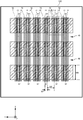
- FIG. 12 is a view showing an example of the semiconductor chip 98 according to the embodiment of the present invention.
- the transistor unit 70 and the diode unit 80 are alternately and periodically arranged in the XY plane.
- FIG. 12 shows an example in which two transistor portions 70 are provided in the X axis direction and five in the Y axis direction, and two diode portions 80 are provided in the X axis direction and six in the Y axis direction.
- FIG. 1 is an enlarged view of the area S of FIG.
- the upper surface side lifetime control area 72 is provided in the area of the broken line in FIG.
- the upper surface side lifetime control region 72 may be provided to include the cathode region 82 of the diode section 80 in the XY plane, as shown in FIG.
- the lower surface side lifetime control area 74 is provided in the area of the dashed dotted line in FIG.
- the lower surface side lifetime control region 74 may be provided from the transistor unit 70 to the diode unit 80.
- the cathode region 82 of the diode section 80 is provided in the depth direction of the semiconductor chip 98 in the top view of FIG. 12.
- the width WI is the width in the Y-axis direction of the transistor portion 70. Further, the width WF is the width in the Y-axis direction of the diode unit 80. The width WI may be larger than the width WF. The width WI may be at least twice and at most 5 times the width WF. The width WI is, for example, 1500 ⁇ m. The width WF is 500 ⁇ m as an example.
- the lower surface side lifetime control region 74 may be provided up to a region E which is outside the upper surface side lifetime control region 72 in the X-axis direction, as shown in FIG. That is, the lower surface side lifetime control region 74 may be provided from the upper surface side lifetime control region 72 to both ends of the semiconductor chip 98 along the X axis.
- FIG. 13 is an enlarged view of a region F in FIG.
- the distance B is a distance from the end Kls to the boundary between the transistor unit 70 and the diode unit 80 in the Y-axis direction.
- the distance C is a distance between the boundary between the transistor unit 70 and the diode unit 80 and the end Klb in the Y-axis direction.
- the distance B may be equal to or greater than 0.01 times and equal to or less than 0.15 times the width WI of the transistor portion 70. Further, the distance C may be not less than 0.015 times and not more than 0.03 times the width WF of the diode section 80.
- the distance A is a distance between the end Kls and the end Klb in the Y-axis direction.
- FIG. 14 is a view showing an example of the gg ′ cross section in FIG.
- the upper surface side lifetime control region 72 is provided from the transistor unit 70 through the diode unit 80 to the transistor unit 70 adjacent to the diode unit 80 on the opposite side in the Y-axis direction.
- the lower surface side lifetime control region 74-1 to the lower surface side lifetime control region 74-4 are formed from each of the transistor portions 70 adjacent on both sides of the diode portion 80 in the Y-axis direction.
- the diode unit 80 is provided.
- the distance D is between the end Klb4 of the lower surface side lifetime control area 74-4 on the Y axis positive side and the end Krb4 of the lower surface side lifetime control area 74-4 on the Y axis negative side in the Y axis direction. Distance.
- the ratio of the distance D to the width WF of the diode unit 80 may be 95% or more and 99% or less.
- the upper surface side lifetime control region 72 is provided from the transistor unit 70 on the Y-axis positive side to the transistor unit 70 on the Y-axis negative side via the diode unit 80.
- the length Ls is a length between the end Kls and the end Krs.
- the length Ls may be larger than the thickness T of the semiconductor substrate 10. By making the length Ls larger than the thickness T, holes generated in the drift region 18 are likely to recombine with electrons. Therefore, the semiconductor device 100 of this example can suppress the switching loss of the transistor unit 70.
- FIG. 15 is a view showing another example of the gg ′ cross section in FIG.
- the semiconductor device 100 of this example is the semiconductor of FIG. 14 in that the lower surface side lifetime control region 74-1 to the lower surface side lifetime control region 74-4 are provided in the entire diode section 80 in the Y-axis direction. It differs from the device 100.
- the lower surface side lifetime control region 74-1 to the lower surface side lifetime control region 74-4 may be provided in the entire Y-axis direction of the diode section 80.
- FIG. 16 is a view showing another example of the gg ′ cross section in FIG.
- the lifetime killer concentration of the lower surface side lifetime control region 74-1 to the lower surface side lifetime control region 74-4 at the boundary between the transistor portion 70 and the diode portion 80 is the lower surface other than the boundary.
- This embodiment differs from the semiconductor device 100 of FIG. 15 in that it is higher than the lifetime killer concentration of the side lifetime control area 74-1 to the lower surface side lifetime control area 74-4.
- the boundary between the transistor portion 70 and the diode portion 80 is indicated by a region U and a region U '.
- the lifetime killer density of the lower surface side lifetime control region 74-1 to the lower surface side lifetime control region 74-4 in the region U and the region U ′ is higher than that in the regions U and U ′. Therefore, in the semiconductor device 100 of the present example, injection of holes from the emitter region 12 of the transistor unit 70 to the cathode region 82 of the diode unit 80 during operation of the diode unit 80 is higher than that of the semiconductor device 100 of FIG. It can suppress more. Therefore, the semiconductor device 100 of this example can further improve the reverse recovery characteristic of the diode unit 80. It should be noted that there is a region where the lower surface side lifetime control region 74-1 to the lower surface side lifetime control region 74-4 are not partially provided in regions other than the region U and the region U ′ in the Y axis direction. May be
- FIG. 17 is a view showing an example of lifetime killer concentration distribution in the Y-axis direction of the lower surface side lifetime control region 74-4 along the line hh ′ in FIG. 15 and the line jj ′ in FIG. is there.
- the lifetime killer concentration of the lower surface side lifetime control region 74-4 in the jj 'cross section is locally high in the region U and the region U'.
- the lifetime killer concentration of the lower surface side lifetime control region 74-4 in the jj ′ cross section is the lifetime killer concentration of the lower surface side lifetime control region 74-4 in the hh ′ cross section It may be 2 to 5 times higher.
- the lifetime killer concentration of the lower surface side lifetime control region 74 is locally high in the regions U and U ′. Therefore, compared with the example of FIG. 15, the semiconductor device 100 of this example can further suppress the injection of holes from the emitter region 12 of the transistor unit 70 to the diode unit 80 when the diode unit 80 operates. Therefore, the semiconductor device 100 of this example can further improve the reverse recovery characteristic of the diode unit 80 as compared with the example of FIG.
- the lifetime killer concentrations of the lower surface side lifetime control region 74-1 in the region U and the region U ′ may be different from each other. Further, the lifetime killer concentration of any of the lower surface side lifetime control region 74-1 to the lower surface side lifetime control region 74-4 may be locally high in the regions U and U '.
- FIG. 18 is a view partially showing an example of the upper surface of another semiconductor device 200 according to this embodiment.
- the semiconductor device 200 shown in FIG. 18 differs from the semiconductor device 100 shown in FIG. 1 in that the floating region 17 of the second conductivity type is provided below the upper surface 21 of the diode section 80.
- Floating region 17 is, for example, of P + type.
- the floating region 17 may be provided at a predetermined distance on the X axis positive side from the end on the X axis negative side of the cathode region 82 in a top view of the semiconductor substrate 10 as shown in FIG.
- the floating region 17 may be provided at a predetermined distance on the Y axis negative side from the end on the Y axis positive side of the cathode region 82 in a top view of the semiconductor substrate 10.
- a plurality of floating regions 17 may be provided in the Y-axis direction in a top view of the semiconductor substrate 10. Although one floating region 17 is illustrated in the X-axis direction in FIG. 18, the region from the region adjacent to the X-axis negative side end of the cathode region 82 to the region adjacent to the X-axis positive side end Plural, in the X-axis direction may be provided. The floating region 17 may be provided inside the cathode region 82 in top view.
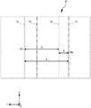
- FIG. 19 is an enlarged view of a region G in FIG.
- the width Wfl1 is the width in the Y-axis direction of the floating region 17, and the width Wfl2 is the width in the X-axis direction of the floating region 17.
- the width Wff1 is a distance between the floating region 17 and another floating region 17 adjacent to the floating region in the Y-axis direction.
- the width Wm is a mesa width of the diode mesa portion 64.
- a plurality of other floating regions 17 may be provided adjacent to the floating region 17 on the X-axis positive side of the floating region 17 shown in FIG. 19 at predetermined intervals.
- the width Wfl1 may be smaller than the width Wm.
- the width Wfl2 may be smaller than the width Wm.
- the width Wff1 may be smaller than the width Wfl1.
- the width Wff1 may be smaller than the width Wfl2.
- FIG. 20 is a view showing an example of a qq 'cross section in FIG.
- the floating region 17 is provided on the lower surface 23 side in the diode section 80.
- the floating region 17 may be provided above the buffer region 20.
- the floating region 17 may be provided in contact with the buffer region 20.
- Floating region 17 is a region in an electrically floating state.
- the electrically floating state indicates a state in which the collector electrode 24 and the emitter electrode 52 are not electrically connected.
- a plurality of floating regions 17 may be provided in the Y-axis direction. Further, a plurality of floating regions 17 may be provided on the X axis positive side of floating region 17 shown in FIG. In the Z-axis direction, floating region 17 may be provided closer to lower surface 23 than lower surface side lifetime control region 74. At least a portion of the floating region 17 may overlap with the lower surface side lifetime control region 74 provided in a portion of the diode section 80 in top view.
- FIG. 20 shows an example in which the floating area 17 provided on the most positive side in the Y-axis direction overlaps the lower surface side lifetime control area 74 in top view, but at least a part of the floating area 17 is viewed from above And may overlap the lower surface side lifetime control area 74.
- the at least one floating region 17 may not overlap with the lower surface side lifetime control region 74 in the Y-axis direction.
- FIG. 20 shows an example in which the floating area 17 excluding the floating area 17 provided on the most positive side in the Y-axis direction does not overlap the lower surface side lifetime control area 74 in the Y-axis direction.
- the distance Ds is a distance from the upper surface 21 of the upper surface side lifetime control area 72 in the Z-axis direction.
- the distance Db is a distance from the lower surface 23 of the lower surface side lifetime control area 74 in the Z-axis direction. Both of the distance Ds and the distance Db may be smaller than half of the thickness T of the semiconductor substrate 10.
- the distance Db may be smaller than the distance Ds.
- the distance Ds may be 10 ⁇ m to 30 ⁇ m.
- the distance Ds is 17 ⁇ m as an example.
- the distance Db may be 5 ⁇ m or more and 20 ⁇ m or less.
- the distance Db is, for example, 10 ⁇ m.
- FIG. 21 is a view showing the qq 'cross section shown in FIG. 20 including the transistor section 70 adjacent on the Y axis negative side of the diode section 80.
- a plurality of floating regions 17 are provided in the diode unit 80 at intervals Wff1 in the Y-axis direction.
- the floating region 17 provided on the most positive side in the Y-axis direction may be provided adjacent to the boundary between the diode unit 80 and the transistor unit 70 adjacent on the Y-axis positive side.
- the floating region 17 provided on the most negative side in the Y-axis direction may be provided adjacent to the boundary between the diode unit 80 and the adjacent transistor unit 70 on the Y-axis negative side.
- the semiconductor device 200 of this example since the floating region 17 is provided in the diode unit 80, injection of electrons from the cathode region 82 can be suppressed. Therefore, the semiconductor device 200 of this example can suppress the surge voltage of the diode unit 80.
- the sum of the widths Wfl1 of the floating regions 17 from the floating region 17 provided on the most positive side in the Y-axis direction to the floating region 17 provided on the most negative side is greater than the width WF in the Y-axis direction of the diode section 80 It may be small. That is, the floating region 17 may cover a portion of the cathode region 82 above the cathode region 82. In other words, a part of the cathode region 82 in the Y-axis direction may not be covered by the floating region 17. In this example, in the semiconductor device 200, a part of the cathode region 82 in the Y-axis direction is not covered by the floating region 17, so that the diode unit 80 can perform diode operation.
- the sum of the widths Wfl1 of the floating regions 17 from the floating region 17 provided on the most positive side in the Y-axis direction to the floating region 17 provided on the most negative side is 65 of the width WF of the diode section 80 in the Y-axis direction. % Or more and 95% or less. More preferably, the sum may be 75% or more and 85% or less of the width WF. In the semiconductor device 200 of this example, since the sum is 65% or more and 95% or less of the width WF, the diode portion 80 can perform diode operation while suppressing the surge voltage of the diode portion 80.
- the distance D is the distance from the end on the Y-axis negative side of the bottom-side lifetime control area 74 on the Y-axis positive side to the end on the Y-axis positive side of the bottom-side lifetime control area 74 on the Y-axis negative side. is there. That is, the distance D is the width in the Y-axis direction of the area where the lower surface side lifetime control area 74 is not provided in the diode section 80.
- the distance D may be larger than the sum of the widths Wfl1 of the floating regions 17 from the floating region 17 provided on the most positive side in the Y-axis direction to the floating region 17 provided on the most negative side.
- the distance D may be 95% or more and 99% or less of the width WF of the diode unit 80 in the Y-axis direction. More preferably, the distance D may be 96% or more and 98% or less of the width WF. That is, the area where the lower surface side lifetime control area 74 is provided may be 1% to 5%, and more preferably 2% to 4%, of the width WF in the Y-axis direction. In the semiconductor device 200 of this example, since the floating region 17 is provided in the diode unit 80, carrier distribution in the depth direction of the semiconductor substrate 10 can be adjusted in the diode unit 80.
- the semiconductor device 200 of the present example since the lower surface side lifetime control region 74 is provided in the transistor portion 70, the holes of the minority carriers generated in the drift region 18 offset the electrons of the majority carrier with a short lifetime. It will be easier. Therefore, the semiconductor device 200 of this example can improve the leak current characteristics of the transistor unit 70. Further, in the semiconductor device 200 of this example, the trade-off between the on-state voltage and the turn-off loss of the transistor unit 70 can be made favorable.
- FIG. 22 is a view showing an example of the upper surface of the semiconductor chip 120 according to the present embodiment.
- the transistor units 70 and the diode units 80 are periodically and alternately arranged in the XY plane.
- FIG. 22 shows an example in which three transistor portions 70 are provided in the X-axis direction and seven in the Y-axis direction, and three diode portions 80 are provided in the X-axis direction and six in the Y-axis direction.
- the dividing unit 46 may be provided.
- the dividing unit 46 may be provided with a gate runner 48 that supplies a gate voltage to the transistor unit 70.
- the width WI is the width in the Y-axis direction of the transistor portion 70.
- the width WF is the width in the Y-axis direction of the diode section 80.
- the width Wh is a width from the end of the well region 11 on the X-axis positive side to the end of the well region 11 on the X-axis negative side, as described later.
- the width is equal to the width of the portion where the base region 14 is provided on the upper surface 21 side of the semiconductor substrate 10 and the well region 11 is not provided.
- the contact region 15 and the emitter region 12 are provided in the region indicated by the width Wh so as to be exposed to the upper surface 21.
- the contact region 15 and the base region 14 are provided in the region indicated by the width Wh so as to be exposed to the upper surface 21.
- the transistor units 70 may be disposed at both ends on the outer circumferential side in the arrangement direction of the transistor unit 70 and the diode unit 80 (Y-axis direction).
- the transistor portion 70 may face the edge termination portion.
- An upper surface side lifetime control region 72 and a lower surface side lifetime control region 74 are provided in the semiconductor chip 120 of this example.
- the range in which the upper surface side lifetime control area 72 and the lower surface side lifetime control area 74 are provided in the upper surface view is indicated by hatched portions.
- the upper surface side lifetime control region 72 and the lower surface side lifetime control region 74 are continuously provided in the X-axis direction across the dividing portion 46 from the edge terminal end on the X-axis positive side to the edge terminal end on the X-axis negative side. It may be done.
- the upper surface side lifetime control region 72 is the Y axis of the transistor portion 70 adjacent on the Y axis negative side of the diode portion 80 from a part of the transistor portion 70 adjacent on the Y axis positive side of the diode portion 80 in the Y axis direction. It may be provided continuously in the Y-axis direction up to a part in the direction. That is, the upper surface side lifetime control region 72 is a transistor adjacent on the Y axis negative side from the transistor portion 70 adjacent on the Y axis positive side of the diode portion 80 so as to cover the entire diode portion 80 in the Y axis direction. It may be provided continuously to the part 70 in the Y-axis direction. The upper surface side lifetime control region 72 may not be provided at the central portion of the transistor unit 70 in the Y-axis direction.
- the lower surface side lifetime control region 74 may be provided continuously in the Y-axis direction from the region adjacent to the diode unit 80 in the transistor unit 70 to the region adjacent to the transistor unit 70 in the diode unit 80. . That is, the lower surface side lifetime control region 74 may be provided continuously in the Y-axis direction from the transistor unit 70 to the diode unit 80 across the boundary between the transistor unit 70 and the diode unit 80.
- the lower surface side lifetime killer may not be provided at the central portion of the diode unit 80 in the Y-axis direction.
- the lower surface side lifetime control region 74 provided in the overlapping region may be another lower surface side lifetime control region 74.
- FIG. 23 is an enlarged view of a region A1 in FIG.
- FIG. 23 is a diagram showing the configuration of the cathode region 82 and the floating region 17 in the diode section 80. As shown in FIG. In FIG. 23, configurations other than the cathode region 82 and the floating region 17 such as the gate trench portion 40 and the dummy trench portion 30 provided in the diode portion 80 and the transistor portion 70 are omitted.
- the semiconductor device 300 of this example in the diode section 80, ten floating regions 17 are provided in the X axis direction and two in the Y axis direction inside the cathode region 82 in the XY plane. Further, in the semiconductor device 300 of this example, the end portion S of the P + -type well region 11 is provided on the X axis positive side of the diode unit 80 and the transistor unit 70. Further, in the semiconductor device 300 of this example, the end S ′ of the P + -type well region 11 is provided on the X axis negative side of the diode unit 80 and the transistor unit 70. In the present example, the well region 11 is provided outside the region where the transistor section 70 and the diode section 80 are alternately arranged. In other words, in the present example, the well region 11 is not provided in the region inside the transistor portion 70 and the diode portion 80 rather than the end portion S.
- a transistor unit 70 is provided adjacent to the diode unit 80 on both the Y-axis positive side and the Y-axis negative side of the diode unit 80.
- the width WI of the transistor unit 70 in the Y-axis direction may be larger than the width WF of the diode unit 80 in the Y-axis direction.
- the width WI may be at least twice and at most 5 times the width WF.
- the width WI may be in the range of 1200 ⁇ m to 2000 ⁇ m.
- the width WI is, for example, 1500 ⁇ m.
- the width WF may be 400 ⁇ m or more and 600 ⁇ m or less.
- the width WF is 500 ⁇ m as an example.
- the width Wh from the end S of the well region 11 on the X axis positive side to the end S ′ of the well region 11 on the X axis negative side may be larger than the width WI.
- the width Wh may be 1.5 times or more and 3 times or less the width WI.
- the width Wh may be in the range of 3000 ⁇ m to 3600 ⁇ m.
- the width Wh is, for example, 3100 ⁇ m.
- the width Wh may be larger than the sum of the width WI and the width WF.
- the semiconductor device 300 of this example suppresses the snapback phenomenon when the transistor portion 70 is turned on or when the diode portion 80 is turned on because the width Wh is larger than the sum of the width WI and the width WF. it can.
- the snapback phenomenon is a phenomenon in which the voltage between the collector electrode 24 and the emitter electrode 52 sharply decreases with an increase in the current flowing between the collector electrode 24 and the emitter electrode 52.
- the upper surface side lifetime control region 72 is a portion of the transistor portion 70 adjacent on the Y-axis positive side of the diode portion 80 in the Y-axis direction on the Y-axis negative side of the diode portion 80. It is provided continuously in the Y-axis direction up to a part of the adjacent transistor portions 70 in the Y-axis direction.
- the upper surface side lifetime control region 72 is continuously provided in the X axis direction from the well region 11 provided on the X axis positive side of the transistor unit 70 and the diode unit 80 to the well region 11 provided on the X axis negative side. Good.
- the area where the upper surface side lifetime control area is provided is indicated by the hatched portion.
- the upper surface side lifetime control region 72 may not be provided in part of the transistor unit 70 in the Y-axis direction.
- the length Ls is a length of the upper surface side lifetime control area 72 in the Y-axis direction.
- the distance B is a distance from the boundary between the diode unit 80 and the transistor unit 70 adjacent on the Y-axis positive side to the end of the upper surface side lifetime control region 72 on the Y-axis positive side.
- the distance B is the distance from the boundary between the diode unit 80 and the transistor unit 70 adjacent to the Y-axis negative side to the end of the upper surface side lifetime control region 72 on the Y-axis negative side.
- the lower surface side lifetime control region 74 extends from the region adjacent to the diode unit 80 in the transistor unit 70 to the region adjacent to the transistor unit 70 in the diode unit 80 in the Y-axis direction. It is provided continuously to That is, in the present example, the lower surface side lifetime control region 74 is provided continuously in the Y-axis direction from the transistor unit 70 to the diode unit 80 across the boundary between the transistor unit 70 and the diode unit 80.
- the length Lb is a length of the lower surface side lifetime control area 74 in the Y-axis direction.
- the lower surface side lifetime killer is not provided at the central portion of the diode unit 80 in the Y-axis direction. Further, in the present embodiment, in the top view of the semiconductor substrate 10, the region overlapping the boundary between the diode unit 80 and the transistor unit 70 adjacent on the Y-axis positive side and the boundary between the transistor unit 70 adjacent on the Y-axis negative side.
- the lower surface side lifetime control area 74 is provided in each of the overlapping areas.
- the lower surface side lifetime control region 74 may be provided to overlap a part of the floating region 17 in the Y-axis direction on the boundary side between the transistor unit 70 and the diode unit 80 in a top view.
- the distance C is a distance from the boundary between the transistor unit 70 adjacent on the Y-axis positive side of the diode unit 80 and the end on the Y-axis negative side of the lower surface side lifetime control region 74. Further, the distance C is a distance from the boundary between the transistor unit 70 adjacent on the Y-axis negative side of the diode unit 80 and the end on the Y-axis positive side of the lower surface side lifetime control region 74.
- Distance D is the Y-axis direction from the end on the Y-axis negative side of the bottom-side lifetime control area 74 on the Y-axis positive side to the end on the Y-axis positive side of the bottom-side lifetime control area 74 on the Y-axis negative side Is the distance at The distance A is a distance in the Y-axis direction from the end on the Y-axis positive side of the bottom-side lifetime control area 74 on the Y-axis positive side to the end on the Y-axis positive side of the top-surface lifetime control area 72.
- the distance A may be smaller than the distance B. That is, in the transistor unit 70, the lower surface side lifetime control region 74 may be disposed closer to the diode portion 80 than the upper surface side lifetime control region 72.
- the semiconductor device 300 of this example since the distance A is smaller than the distance B, injection of holes from the emitter region 12 of the transistor unit 70 to the cathode region 82 of the diode unit 80 can be suppressed when the diode unit 80 operates. Therefore, the semiconductor device 300 of this example can improve the reverse recovery characteristic of the diode unit 80.
- the distance A may be 0.25 times or more and 0.5 times or less the distance B.
- the distance A may be 50 ⁇ m to 100 ⁇ m.
- the length Lb may be longer than the distance C. That is, the lower surface side lifetime control region 74 provided on the transistor portion 70 side from the boundary is lower than the lower surface side lifetime control region 74 provided on the diode portion 80 side from the boundary between the transistor portion 70 and the diode portion 80 , Y axis direction may be long.
- the semiconductor device 300 of this example since the length Lb is longer than the distance C, the injection of holes from the emitter region 12 of the transistor unit 70 to the cathode region 82 of the diode unit 80 can be suppressed when the diode unit 80 operates. . Therefore, the semiconductor device 300 of this example can improve the reverse recovery characteristic of the diode unit 80.
- FIG. 24 is an enlarged view of a region B1 in FIG.
- FIG. 24 is an enlarged view from the end S of the well region 11 on the X axis positive side of the diode section 80 in FIG. 23 to the end S ′ of the well region 11 on the X axis negative side.
- ten floating regions 17 are provided in the X axis direction and two in the Y axis direction inside the cathode region 82 in the XY plane.
- the width Wwc is the width in the X-axis direction from the end S of the well region 11 on the X-axis positive side to the end of the cathode region 82 on the X-axis positive side.
- the width Wwc is the width in the X-axis direction from the end S ′ of the well region 11 on the X-axis negative side to the end of the cathode region 82 on the X-axis negative side.
- the width Wwc may be smaller than the width WF of the diode unit 80.
- the width Wwc may be not less than 0.25 times and not more than 0.75 times the width WF.
- the width Wwc may be 150 ⁇ m or more and 300 ⁇ m or less.
- the width Wwc is, for example, 250 ⁇ m.
- a plurality of contact holes 54 are provided side by side in the Y-axis direction. Although one contact hole 54 is shown in FIG. 24, in fact, as apparent from the top views shown in FIGS. 1 and 18, the position in the X-axis direction is the end of the contact hole 54.
- a plurality of contact holes 54 equal to the position of T and equal to the position of the end T ′ of the contact hole 54 are provided in the Y-axis direction.
- the width Wwca is a width in the X-axis direction between the end S on the X-axis positive side of the well region 11 and the end T on the X-axis positive side of the contact hole 54.
- the width Wwca is the width in the X-axis direction between the end S ′ on the X-axis negative side of the well region 11 and the end T ′ on the X-axis negative side of the contact hole 54.
- the end T on the X-axis positive side of the contact hole 54 is provided away from the end S on the X-axis positive side of the well region 11 by a width Wwca on the X-axis negative side.
- the end T ′ on the X axis negative side of the contact hole 54 is provided away from the end S ′ on the X axis negative side of the well region 11 by a width Wwca on the X axis positive side.
- the contact hole 54 may be provided continuously in the X-axis direction from the end T to the end T ′.
- the width Wwcb is a width in the X-axis direction between the end T of the contact hole 54 and the end of the cathode region 82 on the X-axis positive side.
- the width Wwcb is the width in the X-axis direction between the end T ′ of the contact hole 54 and the end of the cathode region 82 on the X-axis negative side.
- the width Wwca may be smaller than the width Wwcb.
- the width Wwca may be not less than 0.1 times and not more than 0.9 times the width Wwcb.
- the width Wwca may be not less than 20 ⁇ m and not more than 110 ⁇ m.
- the width Wwcb may be 120 ⁇ m or more and 180 ⁇ m or less.
- the width Wwca is, for example, 100 ⁇ m.
- the width Wwcb is, for example, 150 ⁇ m.
- the sum of the width Wwca and the width Wwcb is the width Wwc.
- a floating region 17 is provided inside of the cathode region 82 in the XY plane. Floating region 17 is not electrically connected to any of collector electrode 24 and emitter electrode 52.
- the floating regions 17 are provided in a lattice shape in the XY plane.
- the lattice shape refers to a state in which the floating regions 17 are periodically arranged in both the X-axis direction and the Y-axis direction.
- two floating regions 17 are provided in the Y-axis direction, and ten floating regions 17 are provided in the X-axis direction.
- the opening region 85 is a region between two floating regions 17 provided adjacent to each other in the X-axis direction in the X-axis direction. Further, the opening area 85 is an area between two floating areas 17 provided adjacent to each other in the Y-axis direction in the Y-axis direction. In the present example, ten floating regions 17 are provided across the opening region 85 from the X-axis negative side of the cathode region 82 to the X-axis positive side.
- the width Wff2 is the width in the X-axis direction of the opening region 85.
- the width Wff2 is smaller than the width Wfl2 of the floating region 17 in the X-axis direction.
- the width Wff2 may be smaller than the width WF of the diode unit 80.
- the width Wff2 may be not less than 0.01 times and not more than 0.05 times the width WF.
- the width Wff2 may be 6 ⁇ m or more and 20 ⁇ m or less.
- the width Wff2 is 10 ⁇ m as an example.
- the width Wfl2 of the floating region 17 in the X-axis direction may be smaller than the width WF of the diode section 80.
- the width Wfl2 may be not less than 0.25 times and not more than 0.75 times the width WF.
- the width Wfl2 may be 150 ⁇ m or more and 300 ⁇ m or less.
- the width Wfl2 is 240 ⁇ m as an example.
- the width Wfl1 of the floating region 17 in the Y-axis direction may be smaller than the width WF of the diode section 80.
- the width Wfl1 may be not less than 0.25 times and not more than 0.75 times the width WF.
- the width Wfl1 may be 150 ⁇ m or more and 300 ⁇ m or less.
- the width Wfl1 may be equal to or different from the width Wfl2.
- the width Wfl1 is 240 ⁇ m as an example.
- the width Wcf2 is a width in the X-axis direction between the X-axis positive end of the cathode region 82 and the X-axis positive end of the floating region 17 disposed on the most positive side in the X-axis direction.
- the width Wcf2 may be smaller than the width Wff2.
- the width Wcf2 may be not less than 0.1 times and not more than 0.9 times the width Wff2.
- the width Wcf2 may not be zero.
- the width Wcf2 may be 2 ⁇ m or more and 6 ⁇ m or less.
- the width Wcf2 is 5 ⁇ m as an example.
- the width in the X-axis direction between the X-axis negative side end of the cathode region 82 and the X-axis negative side end of the floating region 17 disposed on the most negative side in the X-axis direction is also equal to the width Wcf2.
- the width Wff1 is the width in the Y-axis direction of the opening region 85.
- the width Wff1 may be smaller than the width Wfl1.
- the width Wff1 may be smaller than the width WF of the diode unit 80.
- the width Wff1 may be not less than 0.01 times and not more than 0.05 times the width WF of the diode section 80.
- the width Wff1 may be 6 ⁇ m or more and 20 ⁇ m or less.
- the width Wff1 may be equal to or different from the width Wff2.
- the width Wff1 is 10 ⁇ m as an example.
- the total area of the plurality of floating regions 17 disposed inside the cathode region 82 in the XY plane may be smaller than the area of the cathode region 82 in the XY plane.
- the total area of the plurality of floating regions 17 in the XY plane may be 50% or more and 99% or less of the area of the cathode region 82 in the XY plane.
- Wh is 3100 ⁇ m
- Wwc is 250 ⁇ m
- Wfl2 and Wfl1 are 240 ⁇ m
- Wcf2 and Wcf1 are 5 ⁇ m
- Wff2 and Wff1 are 10 ⁇ m
- the plurality of floating regions 17 occupy the area of cathode region 82 in the XY plane.
- the total area is 88.6%. That is, a part of the cathode region 82 may not be covered by the floating region 17. In the semiconductor device 300 of this example, since the cathode region 82 is not partially covered by the floating region 17, the diode unit 80 can perform diode operation.
- the width Wcf1 is a width from the end on the Y-axis positive side of the cathode region 82 to the end on the Y-axis positive side of the floating region 17 on the Y-axis positive side.
- the width Wcf1 is the width from the end on the Y axis negative side of the cathode region 82 to the end on the Y axis negative side of the floating region 17 on the Y axis negative side.
- the width Wcf1 may be smaller than the width WF of the diode unit 80.
- the width Wcf1 may be not less than 0.01 times and not more than 0.05 times the width WF.
- the width Wcf1 may not be zero. Further, the width Wcf1 may be equal to or different from the width Wcf2.
- the width Wcf1 may be 2 ⁇ m or more and 6 ⁇ m or less.
- the width Wcf1 is 5 ⁇ m as an example.
- the width Wcnt is a width in the arrangement direction (Y-axis direction) of the contact holes 54.
- the width Wcnt may be smaller than Wff2.
- the width Wcnt may be smaller than Wff1.
- the width Wcnt may be smaller than Wcf2.
- the width Wcnt may be smaller than Wcf1.
- the width Wcnt may be 0.3 ⁇ m or more and 0.7 ⁇ m or less.
- the width Wcnt is 0.5 ⁇ m as an example.
- the upper surface side lifetime control region 72 is provided on the entire surface of the region B1 in top view.
- the lower surface side lifetime control area 74 is continuously provided from the X axis positive side of the area B in the X axis direction to the negative side.
- the lower surface side lifetime control region 74 includes a region overlapping the boundary between the diode unit 80 and the transistor unit 70 adjacent to the diode unit 80 on the Y-axis positive side and the transistor unit 70 adjacent on the Y-axis negative side. It is provided in the area
- the lower surface side lifetime control region 74 is not provided at the central portion of the diode portion 80 in the Y-axis direction.
- the distance C is a distance from the boundary between the transistor unit 70 adjacent on the Y-axis positive side of the diode unit 80 and the end on the Y-axis negative side of the lower surface side lifetime control region 74. Further, the distance C is a distance from the boundary between the transistor unit 70 adjacent on the Y-axis negative side of the diode unit 80 and the end on the Y-axis positive side of the lower surface side lifetime control region 74.
- Distance D is the Y-axis direction from the end on the Y-axis negative side of the bottom-side lifetime control area 74 on the Y-axis positive side to the end on the Y-axis positive side of the bottom-side lifetime control area 74 on the Y-axis negative side Is the distance at That is, the distance D is the width of the area where the lower surface side lifetime control area 74 is not provided in the Y-axis direction.
- FIG. 25 is an enlarged view of a region B2 in FIG.
- the width Wcf2 is a width in the X-axis direction between an end on the X-axis positive side of the cathode region 82 and an end on the X-axis positive side of the floating region 17 disposed on the most positive side in the X-axis direction. It is.
- the width Wcf1 is the width in the Y-axis direction between the end on the Y-axis positive side of the cathode region 82 and the end on the Y-axis positive side of the floating region 17 on the Y-axis positive side.
- the width Wcf1 is 5 ⁇ m as an example.
- the width Wff2 is the width in the X-axis direction of the opening region 85.
- the width Wfl2 is the width of the floating region 17 in the X-axis direction.
- the width Wcf2 may be smaller than the width Wfl2.
- injection of electrons from the cathode region 82 can be suppressed at the end of the diode section 80.
- the distance C is a distance in the Y-axis direction between the boundary between the diode unit 80 and the transistor unit 70 adjacent on the Y-axis positive side and the end of the lower surface side lifetime control region 74 on the Y-axis negative side.
- FIG. 26 is a view showing an example of the h-h 'cross section in FIG.
- the high-concentration region 19 of the first conductivity type may be provided below the base region 14 provided on the upper surface 21.
- the high concentration region 19 of this example is, for example, an N + -type.
- the high concentration region 19 may not be provided in the diode unit 80.
- a plurality of high concentration regions 19 may be provided in the Z-axis direction.
- two high concentration regions 19 are provided, ie, a high concentration region 19-1 and a high concentration region 19-2.
- An N-type region is provided between the high concentration region 19-1 and the high concentration region 19-2 in the Z-axis direction.
- the doping concentration in the N-type region may be lower than the high concentration region 19-1 and the high concentration region 19-2.
- the doping concentration in the N-type region may be equal to the doping concentration of the drift region 18 or higher than the doping concentration of the drift region 18.
- the concentration of holes decreases due to the charge neutral condition, as compared with the drift region 18. That is, the high concentration region 19 suppresses the injection of holes from the base region 14 to the drift region 18. Therefore, the semiconductor device 300 of this example can significantly reduce the injection efficiency of minority carriers from the base region 14 to the drift region 18.
- the minority carrier injection efficiency is reduced as the number of high concentration regions 19 increases. Therefore, as the number of high concentration regions 19 increases, the reverse recovery characteristics of the diode unit 80, particularly the recovery current, is significantly reduced.
- the floating region 17 is provided in the buffer region 20 provided above the cathode region 82 in the diode unit 80.
- two floating regions 17 are provided in the Y-axis direction in the h-h 'cross section.
- boundary position P1 is a boundary position on the Y axis positive side.
- boundary position P1 ′ is a boundary position on the Y axis negative side.
- Boundary positions P1 and P1 ′ are boundary positions in a cross section parallel to the h ⁇ h ′ cross section.
- the hh ′ cross section is a plane perpendicular to the lower surface 23 and parallel to the arrangement direction of the dummy trench portions 30.
- the end position P2 is a position in the Y-axis direction of the end closest to the boundary position P1 of the floating region 17 disposed on the Y-axis positive side. Further, the end position P2 'is a position in the Y axis direction of the end closest to the boundary position P1' of the floating region 17 disposed on the Y axis negative side.
- a plurality of floating regions 17 may be provided in the Y-axis direction from the end position P2 to the end position P2 ′. In this example, two floating regions 17 are provided in the Y-axis direction from the end position P2 to the end position P2 ′.
- the opening region 85 in which the floating region 17 is not provided is present at the depth position substantially the same as the floating region 17 in the Z-axis direction.
- the open area 85 may refer to an area sandwiched by the floating area 17 in the Y-axis direction.
- the open area 85 is an N + -type area.
- the doping concentration of the opening region 85 may be substantially the same as the doping concentration of the drift region 18 or the buffer region 20.
- the open area 85 may be the drift area 18 or the buffer area 20 remaining without forming the floating area 17.
- the width Wcf1 is a width from the end position P1 to the end position P2.
- the width Wcf1 is a width from the end position P1 ′ to the end position P2 ′.
- the width Wff1 is an interval between two floating regions 17 adjacent to each other across the opening region 85 in the Y-axis direction.
- the width Wcf1 may be smaller than the width Wff1.
- the width Wcf1 may be half or less of the width Wff1 or may be 1/4 or less.
- the width Wcf1 may not be zero. In the semiconductor device 300 of this example, since the width Wcf1 is small, the injection of electrons from the cathode region 82 can be suppressed at the end of the diode unit 80.
- the width Wd is the width in the Z-axis direction of the floating region 17.
- the width Wd may be smaller than the width Wcf1.
- the width Wd may be not less than 0.05 times and not more than 0.5 times the width Wcf1.
- the width Wd may be 0.3 ⁇ m or more and 1 ⁇ m or less.
- the width Wd is 0.5 ⁇ m as an example.
- the upper surface side lifetime control region 72 is provided on the upper surface 21 side. Further, the lower surface side lifetime control area 74 is provided on the lower surface 23 side.
- the peak of the lifetime killer concentration of the upper surface side lifetime control area 72 is provided at the position of the distance Ds from the upper surface 21 to the Z axis negative side.
- the peak of the lifetime killer concentration of the lower surface side lifetime control region 74 is provided at the position of the distance Db on the Z axis positive side from the lower surface 23.
- Both of the distance Ds and the distance Db may be smaller than half of the thickness T of the semiconductor substrate 10.
- the distance Db may be smaller than the distance Ds.
- the distance Ds may be 10 ⁇ m to 30 ⁇ m.
- the distance Ds is 17 ⁇ m as an example.
- the distance Db may be 5 ⁇ m or more and 20 ⁇ m or less.
- the distance Db is, for example, 10 ⁇ m.
- the upper surface side lifetime control region 72 is provided entirely in the Y-axis direction in the h-h 'cross section. That is, in the present embodiment, the upper surface side lifetime control region 72 passes the diode portion 80 from the transistor portion 70 adjacent to the Y axis positive side of the diode portion 80 to the transistor portion 70 adjacent to the Y axis positive side. It is provided continuously in the axial direction.
- the distance C is a distance in the Y-axis direction from the boundary between the transistor section 70 adjacent on the Y-axis positive side of the diode section 80 and the end on the Y-axis negative side of the lower surface side lifetime control region 74. Further, the distance C is a distance in the Y-axis direction from the boundary between the transistor unit 70 adjacent on the Y-axis negative side of the diode unit 80 and the end on the Y-axis positive side of the lower surface side lifetime control region 74.
- the distance D is the Y axis between the end on the Y axis negative side of the bottom side lifetime control area 74 on the Y axis positive side and the end on the Y axis positive side of the bottom side lifetime control area 74 on the Y axis negative side. It is the distance in the direction. That is, the distance D is the width of the area where the lower surface side lifetime control area 74 is not provided in the Y-axis direction.
- the distance D may be 95% or more and 99% or less of the width WF. More preferably, the distance D may be 98% of the width WF. That is, the area where the lower surface side lifetime control area 74 is provided may be 1% to 5%, and more preferably 2% to 4%, of the width WF in the Y-axis direction. In the semiconductor device 300 of this example, since the floating region 17 is provided in the diode unit 80, carrier distribution in the depth direction of the semiconductor substrate 10 can be adjusted in the diode unit 80.
- the semiconductor device 300 of this example since the lower surface side lifetime control region 74 is provided in the transistor unit 70, the holes of the minority carriers generated in the drift region 18 offset the electrons of the majority carrier with a short lifetime. It will be easier. Therefore, the semiconductor device 300 of this example can improve the leakage current characteristics of the transistor unit 70. Further, in the semiconductor device 300 of this example, the trade-off between the on voltage and the turn off loss of the transistor unit 70 can be made favorable.
- FIG. 27 is a view showing an example of a cross section taken along the line jj 'of FIG.
- the jj 'cross section is an XZ plane passing through the J' '-J' '' line in FIG.
- the floating region 17 is provided in the buffer region 20 provided above the cathode region 82 in the diode unit 80.
- the upper surface side lifetime control region 72 is provided on the upper surface 21 side in the jj 'cross section. In the jj 'cross section, the lower surface side lifetime control area 74 is not provided on the lower surface 23 side.
- the boundary position P5 is a position in the X-axis direction of the boundary on the X-axis negative side.
- the boundary position P5 ' is the position in the X axis direction of the boundary on the positive side of the X axis.
- the boundary positions P5 and P5 ' are boundary positions in a cross section parallel to the jj' cross section.
- the jj ′ cross section is a plane perpendicular to the lower surface 23 and parallel to the extension direction of the dummy trench portion 30.
- the end position P6 is a position in the X-axis direction of the end closest to the boundary position P5 of the floating region 17 disposed on the most negative side in the X-axis direction.
- the end position P6 ′ is the position in the X axis direction of the end closest to the boundary position P5 ′ of the floating region 17 disposed on the most positive side in the X axis direction.
- an open area 85 where the floating area 17 is not provided is present at substantially the same depth position as the floating area 17 in the Z-axis direction.
- the open area 85 may refer to an area sandwiched by the floating area 17 in the X-axis direction.
- the open area 85 is an N + -type area.
- the doping concentration of the opening region 85 may be substantially the same as the doping concentration of the drift region 18 or the buffer region 20.
- the open area 85 may be the drift area 18 or the buffer area 20 remaining without forming the floating area 17.
- the width Wfl2 is the width of the floating region 17 in the X-axis direction.
- the width Wcf2 is a width in the X-axis direction between the boundary position P5 and the end position P6.
- the width Wcf2 is the width in the X-axis direction between the boundary position P5 'and the end position P6'.
- the width Wff2 is the distance between two floating regions 17 adjacent to each other across the opening region 85 in the X-axis direction.
- the width Wcf2 may be smaller than the width Wff2.
- the floating region 17 is provided in a lattice shape in the XY plane in the diode unit 80, a surge voltage (overshoot voltage) at the time of reverse recovery of the diode unit 80 can be suppressed.
- FIG. 28 is another enlarged view of the area A1 in FIG. Similar to the semiconductor device 300 shown in FIG. 23, in the semiconductor device 300 of this example, the transistor portion 70 is provided adjacent to the diode portion 80 on the Y axis positive side and the negative side of the diode portion 80.
- the semiconductor device 300 of this example is different from the semiconductor device 300 shown in FIG. 23 in the arrangement of the floating region 17 in the diode unit 80.
- the floating region 17 in the diode unit 80, is inside the cathode region 82 in the XY plane, from the Y axis positive side boundary side of the cathode region 82 indicated by the broken line portion. It is provided continuously to the boundary side.
- the floating region 17 is continuously provided in the Y-axis direction in the X-axis direction at any position in the Y-axis direction from the boundary side on the Y-axis positive side of the cathode region 82 to the boundary side on the Y-axis negative side. , There is no area where the floating area 17 is not provided.
- FIG. 29 is an enlarged view of a region C1 in FIG.
- FIG. 29 is an enlarged view from the end S of the well region 11 on the X axis positive side of the diode section 80 in FIG. 28 to the end S ′ of the well region 11 on the X axis negative side.
- floating regions 17 are provided in a stripe shape in the XY plane.
- the stripe shape refers to a state in which a plurality of rectangular floating regions 17 are provided at predetermined intervals in the direction of the short side of the rectangle.
- the floating region 17 in this example has a rectangular shape whose long side is in the Y-axis direction and whose short side is in the X-axis direction.
- a plurality of floating regions 17 are provided in the X axis direction from the most negative side to the most positive side in the X axis direction of the cathode region 82.
- the width Wff2 ' is a width in the X-axis direction between two floating regions 17 provided adjacent to each other in the X-axis direction.
- the width Wff2 ' may be smaller than the width WF of the diode unit 80.
- the width Wff2 ' may be not less than 0.01 times and not more than 0.05 times the width WF.
- the width Wff2 ′ may be 6 ⁇ m or more and 20 ⁇ m or less.
- the width Wff2 ' is 10 ⁇ m as an example.
- the width Wfl2 ' is the width of the floating region 17 in the X-axis direction.
- the width Wfl2 ' may be smaller than the width WF of the diode unit 80.
- the width Wfl2 ' may be 0.04 times or more and 0.13 times or less the width WF.
- the width Wfl2 ' may be 25 ⁇ m or more and 50 ⁇ m or less.
- the width Wfl2 ' is 40 ⁇ m as an example.
- the width Wfl1 ' is the width of the floating region 17 in the Y-axis direction.
- the width Wfl1 ' may be smaller than the width WF of the diode unit 80.
- the width Wfl1 ' may be 0.5 times or more and 0.99 times or less the width WF.
- the width Wfl1 ′ may be 440 ⁇ m or more and 540 ⁇ m or less.
- the width Wfl1 ' is, for example, 490 ⁇ m.
- the width Wcf2 is a width in the X-axis direction between the end on the X-axis positive side of the cathode region 82 and the end on the X-axis positive side of the floating region 17 disposed on the most positive side in the X-axis direction.
- the width Wcf2 is the width in the X-axis direction between the end on the X-axis negative side of the cathode region 82 and the end on the X-axis negative side of the floating region 17 disposed on the most negative side in the X-axis direction. .
- the width Wcf2 may be smaller than the width Wff2 '.
- the width Wcf2 may be not less than 0.1 times and not more than 0.9 times the width Wff2 '.
- the width Wcf2 may not be zero.
- the width Wcf2 may be 2 ⁇ m or more and 6 ⁇ m or less.
- the width Wcf2 is 5 ⁇ m as an example.
- the total area of the plurality of floating regions 17 disposed inside the cathode region 82 in the XY plane may be smaller than the area of the cathode region 82 in the XY plane.
- the total area of the plurality of floating regions 17 in the XY plane may be 50% or more and 99% or less of the area of the cathode region 82 in the XY plane.
- Wh is 3100 ⁇ m
- Wwc is 250 ⁇ m
- Wfl2 ′ is 40 ⁇ m
- Wfl1 ′ is 490 ⁇ m
- Wcf2 and Wcf1 are 5 ⁇ m
- Wff2 ′ is 10 ⁇ m
- the floating region 17 is inside the cathode region 82 in top view.
- the diode unit 80 can perform diode operation.
- the width Wcf1 in the Y-axis direction between the end on the Y-axis positive side of the cathode region 82 and the end on the Y-axis positive side of the floating region 17 may be smaller than the width WF of the diode section 80.
- the width Wcf1 may be not less than 0.01 times and not more than 0.05 times the width WF. Further, the width Wcf1 may be equal to or different from the width Wcf2.
- the width Wcf1 may not be zero.
- the width Wcf1 may be 2 ⁇ m or more and 6 ⁇ m or less.
- the width Wcf1 is 5 ⁇ m as an example.
- the width from the Y-axis negative end of the cathode region 82 to the Y-axis negative end of the floating region 17 may be equal to the width Wcf1.
- the upper surface side lifetime control region 72 is provided on the entire surface of the region B1 in top view.
- the lower surface side lifetime control area 74 is continuously provided from the X axis positive side of the area B to the negative side in the X axis direction.
- the lower surface side lifetime control region 74 includes a region overlapping the boundary between the diode unit 80 and the transistor unit 70 adjacent to the diode unit 80 on the Y-axis positive side and the transistor unit 70 adjacent on the Y-axis negative side. It is provided in the area
- the lower surface side lifetime control region 74 is not provided at the central portion of the diode portion 80 in the Y-axis direction.
- the distance C is a distance in the Y-axis direction from the boundary between the transistor section 70 adjacent on the Y-axis positive side of the diode section 80 and the end on the Y-axis negative side of the lower surface side lifetime control region 74. Further, the distance C is a distance in the Y-axis direction from the boundary between the transistor unit 70 adjacent on the Y-axis negative side of the diode unit 80 and the end on the Y-axis positive side of the lower surface side lifetime control region 74.
- the distance D is Y between the end on the Y axis negative side of the bottom side lifetime control area 74 on the Y axis positive side and the end on the Y axis positive side of the bottom side lifetime control area 74 on the Y axis negative side. It is the distance in the axial direction. That is, the distance D is the width of the area where the lower surface side lifetime control area 74 is not provided in the Y-axis direction.
- FIG. 30 is an enlarged view of a region C2 in FIG.
- the width Wcf2 is a width in the X-axis direction between an end on the X-axis positive side of the cathode region 82 and an end on the X-axis positive side of the floating region 17 disposed on the most positive side in the X-axis direction. It is.
- the width Wcf1 is a width in the Y-axis direction between the end on the Y-axis positive side of the cathode region 82 and the end on the Y-axis positive side of the floating region 17.
- the width Wcf1 is 5 ⁇ m as an example.
- the width Wff2 ' is the width in the X-axis direction of the opening region 85.
- the width Wfl2 ' is the width of the floating region 17 in the X-axis direction.
- the distance C is a distance in the Y axis direction from the boundary between the diode section 80 and the transistor section 70 adjacent on the Y axis positive side to the end of the lower surface side lifetime control area 74 on the Y axis negative side.
- FIG. 31 is a view showing an example of the kk 'cross section in FIG.
- the floating region 17 is provided in the buffer region 20 provided above the cathode region 82 in the diode unit 80.
- the floating region 17 in this example is continuously provided from the Y axis positive side to the negative side in the kk ′ cross section.
- the width Wcf1 is the distance between the end position P1 and the end position P2, as in the example of FIG. Further, the width Wcf1 is a distance between the end position P1 'and the end position P2'.
- the width Wd of the floating region 17 in the Z-axis direction may be smaller than the width Wcf1.
- the width Wcf1 may be 0.05 times or more and 0.5 times or less the width Wd.
- the width Wd may be 0.3 ⁇ m or more and 1 ⁇ m or less.
- the width Wd is 0.5 ⁇ m as an example.
- the width Wcf1 may be smaller than the width Wfl1. In the semiconductor device 300 of this example, since the width Wcf1 is small, the injection of electrons from the cathode region 82 can be suppressed at the end of the diode unit 80.
- the upper surface side lifetime control region 72 is provided on the upper surface 21 side. Further, the lower surface side lifetime control area 74 is provided on the lower surface 23 side.
- the peak of the lifetime killer concentration of the upper surface side lifetime control area 72 is provided at the position of the distance Ds from the upper surface 21 on the Z axis negative side.
- the peak of the lifetime killer concentration of the lower surface side lifetime control area 74 is provided at the position of the distance Db on the Z axis positive side from the lower surface 23.
- the upper surface side lifetime control region 72 is provided on the entire Y-axis direction in the kk ′ cross section. That is, in the present embodiment, the upper surface side lifetime control region 72 passes the diode portion 80 from the transistor portion 70 adjacent to the Y axis positive side of the diode portion 80 to the transistor portion 70 adjacent to the Y axis positive side. It is provided continuously in the axial direction.
- the distance C is a distance in the Y-axis direction from the boundary between the transistor section 70 adjacent on the Y-axis positive side of the diode section 80 and the end on the Y-axis negative side of the lower surface side lifetime control region 74. Further, the distance C is a distance in the Y-axis direction from the boundary between the transistor unit 70 adjacent on the Y-axis negative side of the diode unit 80 and the end on the Y-axis positive side of the lower surface side lifetime control region 74.
- the distance D is the Y axis between the end on the Y axis negative side of the bottom side lifetime control area 74 on the Y axis positive side and the end on the Y axis positive side of the bottom side lifetime control area 74 on the Y axis negative side. It is the distance in the direction. That is, the distance D is the width of the area where the lower surface side lifetime control area 74 is not provided in the Y-axis direction.
- the distance D may be 95% or more and 99% or less of the width WF of the diode unit 80. More preferably, the distance D may be 98% of the width WF. That is, in the present embodiment, the area where the lower surface side lifetime control area 74 is provided may be 1% or more and 5% or less of the width WF, and more preferably 2% in the Y-axis direction. In the semiconductor device 300 of this example, since the floating region 17 is provided in the diode unit 80, carrier distribution in the depth direction of the semiconductor substrate 10 can be adjusted in the diode unit 80.
- the semiconductor device 300 of this example since the lower surface side lifetime control region 74 is provided in the transistor unit 70, the holes of the minority carriers generated in the drift region 18 offset the electrons of the majority carrier with a short lifetime. It will be easier. Therefore, the semiconductor device 300 of this example can improve the leakage current characteristics of the transistor unit 70. Further, in the semiconductor device 300 of this example, the trade-off between the on voltage and the turn off loss of the transistor unit 70 can be made favorable.
- FIG. 32 is a view showing an example of the m-m 'cross section in FIG.
- the m-m 'cross section is an XZ plane passing through the m' '-m' '' line in FIG.
- the floating region 17 is provided in the buffer region 20 provided above the cathode region 82 in the diode unit 80.
- the upper surface side lifetime control region 72 is provided on the upper surface 21 side in the m-m 'cross section.
- the lower surface side lifetime control region 74 is not provided on the lower surface 23 side in the m-m 'cross section.
- the mm ′ cross section is a plane which is perpendicular to the lower surface 23 of the semiconductor substrate 10 and parallel to the extending direction of the dummy trench portion 30. Also in this example, as in the example of FIG. 27, in the Z-axis direction, an open area 85 in which the floating area 17 is not provided is present at the same depth position as the floating area 17.
- the width Wfl2 ' is the width of the floating region 17 in the X-axis direction.
- the width Wcf2 is a distance in the X-axis direction between the boundary position P5 and the end position P6, as in the example of FIG. Further, the width Wcf2 is a distance in the X-axis direction between the boundary position P5 'and the end position P6'. Further, the width Wff2 'is an interval between the floating regions 17 adjacent to each other across the opening region 85 in the X-axis direction.
- the width Wcf2 may be smaller than the width Wff2 '.
- the semiconductor device 300 of this example in the diode unit 80, a plurality of floating regions 17 are provided across the opening region 85 from the end position P6 to the end position P6 ′. Further, in the semiconductor device 300 of this example, the floating regions 17 are provided in the form of stripes in the XY plane. Therefore, the semiconductor device 300 of this example can suppress the surge voltage at the time of reverse recovery of the diode unit 80.
Landscapes
- Metal-Oxide And Bipolar Metal-Oxide Semiconductor Integrated Circuits (AREA)
Abstract
La présente invention concerne un dispositif à semi-conducteur comprenant : un substrat semi-conducteur ayant une région de dérive de premier type de conductivité; une partie transistor disposée dans le substrat semi-conducteur; et une partie diode disposée dans le substrat semi-conducteur et disposée conjointement avec la partie transistor le long d'une direction d'agencement prédéterminée, la partie transistor et la partie diode comprenant une seconde région de base de type de conductivité disposée au-dessus de la région de dérive à l'intérieur du substrat semi-conducteur, une pluralité de sections de tranchée pénétrant chacune dans la région de base à partir de la surface supérieure du substrat semi-conducteur, s'étendant dans une direction d'extension perpendiculaire à la direction d'agencement sur la surface supérieure du substrat semi-conducteur et comprenant une section conductrice à l'intérieur de celle-ci, et une région de commande de durée de vie côté surface inférieure prévue pour s'étendre de la partie transistor à la partie diode sur le côté de surface inférieure du substrat semi-conducteur et comprenant un dispositif de suppression de durée de vie, et la région de commande de durée de vie côté surface inférieure est disposée dans une section de la partie transistor dans la direction d'agencement et non disposée dans les autres sections.
Priority Applications (3)
| Application Number | Priority Date | Filing Date | Title |
|---|---|---|---|
| JP2019529782A JP6747593B2 (ja) | 2017-07-14 | 2018-07-12 | 半導体装置 |
| CN201880005697.8A CN110140199B (zh) | 2017-07-14 | 2018-07-12 | 半导体装置 |
| US16/455,799 US11069529B2 (en) | 2017-07-14 | 2019-06-28 | Semiconductor device with at least one lower-surface side lifetime control region |
Applications Claiming Priority (4)
| Application Number | Priority Date | Filing Date | Title |
|---|---|---|---|
| JP2017138603 | 2017-07-14 | ||
| JP2017-138603 | 2017-07-14 | ||
| JP2017238637 | 2017-12-13 | ||
| JP2017-238637 | 2017-12-13 |
Related Child Applications (1)
| Application Number | Title | Priority Date | Filing Date |
|---|---|---|---|
| US16/455,799 Continuation US11069529B2 (en) | 2017-07-14 | 2019-06-28 | Semiconductor device with at least one lower-surface side lifetime control region |
Publications (1)
| Publication Number | Publication Date |
|---|---|
| WO2019013286A1 true WO2019013286A1 (fr) | 2019-01-17 |
Family
ID=65002074
Family Applications (1)
| Application Number | Title | Priority Date | Filing Date |
|---|---|---|---|
| PCT/JP2018/026339 Ceased WO2019013286A1 (fr) | 2017-07-14 | 2018-07-12 | Dispositif à semi-conducteur |
Country Status (4)
| Country | Link |
|---|---|
| US (1) | US11069529B2 (fr) |
| JP (1) | JP6747593B2 (fr) |
| CN (1) | CN110140199B (fr) |
| WO (1) | WO2019013286A1 (fr) |
Cited By (5)
| Publication number | Priority date | Publication date | Assignee | Title |
|---|---|---|---|---|
| JP2022169322A (ja) * | 2021-04-27 | 2022-11-09 | 株式会社デンソー | 半導体装置 |
| WO2022265061A1 (fr) * | 2021-06-17 | 2022-12-22 | 富士電機株式会社 | Dispositif à semi-conducteur et procédé de production de dispositif à semi-conducteur |
| JPWO2023100454A1 (fr) * | 2021-11-30 | 2023-06-08 | ||
| WO2025258305A1 (fr) * | 2024-06-13 | 2025-12-18 | 富士電機株式会社 | Dispositif à semi-conducteur et procédé de fabrication de dispositif à semi-conducteur |
| WO2026009816A1 (fr) * | 2024-07-02 | 2026-01-08 | 富士電機株式会社 | Dispositif à semi-conducteur et module à semi-conducteur |
Families Citing this family (8)
| Publication number | Priority date | Publication date | Assignee | Title |
|---|---|---|---|---|
| CN105814694B (zh) * | 2014-10-03 | 2019-03-08 | 富士电机株式会社 | 半导体装置以及半导体装置的制造方法 |
| DE102017107174B4 (de) * | 2017-04-04 | 2020-10-08 | Infineon Technologies Ag | IGBT mit dV/dt-Steuerbarkeit und Verfahren zum Verarbeiten eines IGBT |
| DE102017124872B4 (de) | 2017-10-24 | 2021-02-18 | Infineon Technologies Ag | Verfahren zur Herstellung eines IGBT mit dV/dt-Steuerbarkeit |
| DE102017124871B4 (de) | 2017-10-24 | 2021-06-17 | Infineon Technologies Ag | Leistungshalbleiter-Vorrichtung und Verfahren zum Herstellen einer Leistungshalbleiter-Vorrichtung |
| DE102018130095B4 (de) * | 2018-11-28 | 2021-10-28 | Infineon Technologies Dresden GmbH & Co. KG | Halbleiterleistungsschalter mit verbesserter Steuerbarkeit |
| JP7395844B2 (ja) * | 2019-05-14 | 2023-12-12 | 富士電機株式会社 | 半導体装置および製造方法 |
| JP7198236B2 (ja) * | 2020-03-13 | 2022-12-28 | 株式会社東芝 | 半導体装置 |
| JP2025050265A (ja) * | 2023-09-22 | 2025-04-04 | 株式会社東芝 | 半導体装置の製造方法、および半導体装置 |
Citations (5)
| Publication number | Priority date | Publication date | Assignee | Title |
|---|---|---|---|---|
| JP2014056942A (ja) * | 2012-09-12 | 2014-03-27 | Toshiba Corp | 電力用半導体装置 |
| WO2014156849A1 (fr) * | 2013-03-25 | 2014-10-02 | 富士電機株式会社 | Dispositif semi-conducteur |
| WO2015145929A1 (fr) * | 2014-03-25 | 2015-10-01 | 株式会社デンソー | Dispositif à semi-conducteurs |
| JP2015211149A (ja) * | 2014-04-28 | 2015-11-24 | トヨタ自動車株式会社 | 半導体装置及び半導体装置の製造方法 |
| JP2017045949A (ja) * | 2015-08-28 | 2017-03-02 | 株式会社デンソー | 半導体装置 |
Family Cites Families (17)
| Publication number | Priority date | Publication date | Assignee | Title |
|---|---|---|---|---|
| JP2010147381A (ja) * | 2008-12-22 | 2010-07-01 | Denso Corp | 半導体装置の製造方法 |
| EP2477226B1 (fr) * | 2009-09-07 | 2016-06-22 | Toyota Jidosha Kabushiki Kaisha | Dispositif à semi-conducteur comprenant un substrat semiconducteur avec une région de diode et une région igbt |
| JP2011129619A (ja) | 2009-12-16 | 2011-06-30 | Toyota Motor Corp | 半導体装置の製造方法 |
| JP5190485B2 (ja) | 2010-04-02 | 2013-04-24 | 株式会社豊田中央研究所 | 半導体装置 |
| JP5605073B2 (ja) * | 2010-08-17 | 2014-10-15 | 株式会社デンソー | 半導体装置 |
| DE112011105681B4 (de) * | 2011-09-28 | 2015-10-15 | Toyota Jidosha Kabushiki Kaisha | Verfahren zur Herstellung einer Halbleitervorrichtung |
| JP5811861B2 (ja) * | 2012-01-23 | 2015-11-11 | 株式会社デンソー | 半導体装置の製造方法 |
| JP6119593B2 (ja) * | 2013-12-17 | 2017-04-26 | トヨタ自動車株式会社 | 半導体装置 |
| JP2015153784A (ja) * | 2014-02-10 | 2015-08-24 | トヨタ自動車株式会社 | 半導体装置の製造方法及び半導体装置 |
| JP6197773B2 (ja) * | 2014-09-29 | 2017-09-20 | トヨタ自動車株式会社 | 半導体装置 |
| US9559171B2 (en) * | 2014-10-15 | 2017-01-31 | Fuji Electric Co., Ltd. | Semiconductor device |
| JP6018163B2 (ja) | 2014-12-02 | 2016-11-02 | トヨタ自動車株式会社 | 半導体装置 |
| JP2016162807A (ja) * | 2015-02-27 | 2016-09-05 | トヨタ自動車株式会社 | 半導体装置とその製造方法 |
| US10529839B2 (en) * | 2015-05-15 | 2020-01-07 | Fuji Electric Co., Ltd. | Semiconductor device |
| JP6384425B2 (ja) * | 2015-08-21 | 2018-09-05 | 株式会社デンソー | 半導体装置 |
| JP6531589B2 (ja) | 2015-09-17 | 2019-06-19 | 株式会社デンソー | 半導体装置 |
| JP6547724B2 (ja) * | 2016-11-15 | 2019-07-24 | トヨタ自動車株式会社 | 半導体装置の製造方法 |
-
2018
- 2018-07-12 CN CN201880005697.8A patent/CN110140199B/zh active Active
- 2018-07-12 JP JP2019529782A patent/JP6747593B2/ja active Active
- 2018-07-12 WO PCT/JP2018/026339 patent/WO2019013286A1/fr not_active Ceased
-
2019
- 2019-06-28 US US16/455,799 patent/US11069529B2/en active Active
Patent Citations (5)
| Publication number | Priority date | Publication date | Assignee | Title |
|---|---|---|---|---|
| JP2014056942A (ja) * | 2012-09-12 | 2014-03-27 | Toshiba Corp | 電力用半導体装置 |
| WO2014156849A1 (fr) * | 2013-03-25 | 2014-10-02 | 富士電機株式会社 | Dispositif semi-conducteur |
| WO2015145929A1 (fr) * | 2014-03-25 | 2015-10-01 | 株式会社デンソー | Dispositif à semi-conducteurs |
| JP2015211149A (ja) * | 2014-04-28 | 2015-11-24 | トヨタ自動車株式会社 | 半導体装置及び半導体装置の製造方法 |
| JP2017045949A (ja) * | 2015-08-28 | 2017-03-02 | 株式会社デンソー | 半導体装置 |
Cited By (10)
| Publication number | Priority date | Publication date | Assignee | Title |
|---|---|---|---|---|
| JP2022169322A (ja) * | 2021-04-27 | 2022-11-09 | 株式会社デンソー | 半導体装置 |
| JP7600848B2 (ja) | 2021-04-27 | 2024-12-17 | 株式会社デンソー | 半導体装置 |
| WO2022265061A1 (fr) * | 2021-06-17 | 2022-12-22 | 富士電機株式会社 | Dispositif à semi-conducteur et procédé de production de dispositif à semi-conducteur |
| JPWO2022265061A1 (fr) * | 2021-06-17 | 2022-12-22 | ||
| JP7670132B2 (ja) | 2021-06-17 | 2025-04-30 | 富士電機株式会社 | 半導体装置および半導体装置の製造方法 |
| JPWO2023100454A1 (fr) * | 2021-11-30 | 2023-06-08 | ||
| WO2023100454A1 (fr) * | 2021-11-30 | 2023-06-08 | 富士電機株式会社 | Dispositif à semi-conducteur au carbure de silicium et son procédé de fabrication |
| JP7704214B2 (ja) | 2021-11-30 | 2025-07-08 | 富士電機株式会社 | 炭化珪素半導体装置及びその製造方法 |
| WO2025258305A1 (fr) * | 2024-06-13 | 2025-12-18 | 富士電機株式会社 | Dispositif à semi-conducteur et procédé de fabrication de dispositif à semi-conducteur |
| WO2026009816A1 (fr) * | 2024-07-02 | 2026-01-08 | 富士電機株式会社 | Dispositif à semi-conducteur et module à semi-conducteur |
Also Published As
| Publication number | Publication date |
|---|---|
| US20190326118A1 (en) | 2019-10-24 |
| JPWO2019013286A1 (ja) | 2019-11-21 |
| CN110140199A (zh) | 2019-08-16 |
| JP6747593B2 (ja) | 2020-08-26 |
| CN110140199B (zh) | 2022-07-05 |
| US11069529B2 (en) | 2021-07-20 |
Similar Documents
| Publication | Publication Date | Title |
|---|---|---|
| JP6747593B2 (ja) | 半導体装置 | |
| JP7673846B2 (ja) | 半導体装置 | |
| JP6780777B2 (ja) | 半導体装置 | |
| JP5787853B2 (ja) | 電力用半導体装置 | |
| CN108074924B (zh) | 半导体装置 | |
| JP7020570B2 (ja) | 半導体装置およびその製造方法 | |
| US8232593B2 (en) | Power semiconductor device | |
| CN103219339B (zh) | 半导体器件 | |
| US9059238B2 (en) | Semiconductor device | |
| JP7726248B2 (ja) | 半導体装置 | |
| JP2020074396A (ja) | 半導体装置 | |
| JP6733829B2 (ja) | 半導体装置 | |
| JP7414047B2 (ja) | 半導体装置 | |
| WO2017155122A1 (fr) | Dispositif à semi-conducteur | |
| WO2018147466A1 (fr) | Dispositif à semiconducteur | |
| CN110692140A (zh) | 半导体装置 | |
| WO2019098271A1 (fr) | Dispositif à semi-conducteur | |
| US12471303B2 (en) | Semiconductor device having an injection suppression region | |
| JP2020177973A (ja) | 半導体装置 | |
| JP6992476B2 (ja) | 半導体装置 | |
| WO2024214461A1 (fr) | Dispositif à semi-conducteur | |
| WO2024236880A1 (fr) | Dispositif à semi-conducteur |
Legal Events
| Date | Code | Title | Description |
|---|---|---|---|
| 121 | Ep: the epo has been informed by wipo that ep was designated in this application |
Ref document number: 18831927 Country of ref document: EP Kind code of ref document: A1 |
|
| ENP | Entry into the national phase |
Ref document number: 2019529782 Country of ref document: JP Kind code of ref document: A |
|
| NENP | Non-entry into the national phase |
Ref country code: DE |
|
| 122 | Ep: pct application non-entry in european phase |
Ref document number: 18831927 Country of ref document: EP Kind code of ref document: A1 |