WO2019059062A1 - Dispositif d'antenne - Google Patents
Dispositif d'antenne Download PDFInfo
- Publication number
- WO2019059062A1 WO2019059062A1 PCT/JP2018/033784 JP2018033784W WO2019059062A1 WO 2019059062 A1 WO2019059062 A1 WO 2019059062A1 JP 2018033784 W JP2018033784 W JP 2018033784W WO 2019059062 A1 WO2019059062 A1 WO 2019059062A1
- Authority
- WO
- WIPO (PCT)
- Prior art keywords
- line
- dielectric layer
- antenna device
- wiring
- tip
- Prior art date
- Legal status (The legal status is an assumption and is not a legal conclusion. Google has not performed a legal analysis and makes no representation as to the accuracy of the status listed.)
- Ceased
Links
Images





Classifications
-
- H—ELECTRICITY
- H01—ELECTRIC ELEMENTS
- H01Q—ANTENNAS, i.e. RADIO AERIALS
- H01Q21/00—Antenna arrays or systems
- H01Q21/06—Arrays of individually energised antenna units similarly polarised and spaced apart
- H01Q21/061—Two dimensional planar arrays
- H01Q21/065—Patch antenna array
-
- H—ELECTRICITY
- H01—ELECTRIC ELEMENTS
- H01P—WAVEGUIDES; RESONATORS, LINES, OR OTHER DEVICES OF THE WAVEGUIDE TYPE
- H01P5/00—Coupling devices of the waveguide type
- H01P5/02—Coupling devices of the waveguide type with invariable factor of coupling
-
- H—ELECTRICITY
- H01—ELECTRIC ELEMENTS
- H01P—WAVEGUIDES; RESONATORS, LINES, OR OTHER DEVICES OF THE WAVEGUIDE TYPE
- H01P5/00—Coupling devices of the waveguide type
- H01P5/08—Coupling devices of the waveguide type for linking dissimilar lines or devices
-
- H—ELECTRICITY
- H01—ELECTRIC ELEMENTS
- H01P—WAVEGUIDES; RESONATORS, LINES, OR OTHER DEVICES OF THE WAVEGUIDE TYPE
- H01P5/00—Coupling devices of the waveguide type
- H01P5/12—Coupling devices having more than two ports
-
- H—ELECTRICITY
- H01—ELECTRIC ELEMENTS
- H01Q—ANTENNAS, i.e. RADIO AERIALS
- H01Q1/00—Details of, or arrangements associated with, antennas
- H01Q1/48—Earthing means; Earth screens; Counterpoises
-
- H—ELECTRICITY
- H01—ELECTRIC ELEMENTS
- H01Q—ANTENNAS, i.e. RADIO AERIALS
- H01Q21/00—Antenna arrays or systems
- H01Q21/0006—Particular feeding systems
- H01Q21/0075—Stripline fed arrays
-
- H—ELECTRICITY
- H01—ELECTRIC ELEMENTS
- H01Q—ANTENNAS, i.e. RADIO AERIALS
- H01Q5/00—Arrangements for simultaneous operation of antennas on two or more different wavebands, e.g. dual-band or multi-band arrangements
- H01Q5/30—Arrangements for providing operation on different wavebands
- H01Q5/307—Individual or coupled radiating elements, each element being fed in an unspecified way
- H01Q5/314—Individual or coupled radiating elements, each element being fed in an unspecified way using frequency dependent circuits or components, e.g. trap circuits or capacitors
- H01Q5/335—Individual or coupled radiating elements, each element being fed in an unspecified way using frequency dependent circuits or components, e.g. trap circuits or capacitors at the feed, e.g. for impedance matching
-
- H—ELECTRICITY
- H01—ELECTRIC ELEMENTS
- H01Q—ANTENNAS, i.e. RADIO AERIALS
- H01Q5/00—Arrangements for simultaneous operation of antennas on two or more different wavebands, e.g. dual-band or multi-band arrangements
- H01Q5/30—Arrangements for providing operation on different wavebands
- H01Q5/307—Individual or coupled radiating elements, each element being fed in an unspecified way
- H01Q5/342—Individual or coupled radiating elements, each element being fed in an unspecified way for different propagation modes
- H01Q5/357—Individual or coupled radiating elements, each element being fed in an unspecified way for different propagation modes using a single feed point
- H01Q5/364—Creating multiple current paths
- H01Q5/371—Branching current paths
-
- H—ELECTRICITY
- H01—ELECTRIC ELEMENTS
- H01Q—ANTENNAS, i.e. RADIO AERIALS
- H01Q9/00—Electrically-short antennas having dimensions not more than twice the operating wavelength and consisting of conductive active radiating elements
- H01Q9/04—Resonant antennas
- H01Q9/0407—Substantially flat resonant element parallel to ground plane, e.g. patch antenna
- H01Q9/045—Substantially flat resonant element parallel to ground plane, e.g. patch antenna with particular feeding means
- H01Q9/0457—Substantially flat resonant element parallel to ground plane, e.g. patch antenna with particular feeding means electromagnetically coupled to the feed line
Definitions
- the present invention relates to an antenna device.
- Priority is claimed on Japanese Patent Application No. 2017-181339, filed September 21, 2017, the content of which is incorporated herein by reference.
- an antenna apparatus provided with a planar antenna of an electromagnetic coupling feed system is known.
- a rectangular feed slot is formed in a feed slot layer which is a ground layer, and a phased coupler in which a distributor / combiner is electromagnetically coupled to a circular radiating element through the feed slot layer.
- An array antenna arrangement is described.
- the radiation elements are arranged in a zigzag form in a plan view, and power is simultaneously supplied to the respective radiation elements as a pair of two adjacent radiation elements by a branch wiring pattern of the distribution / combination device.
- the impedance at the power supply source and the impedance at the electromagnetic coupling portion to each radiation element depend on the specifications of the device. For example, it is necessary to set the power supply source to a fixed value such as 50 ⁇ and the electromagnetic coupling unit to 120 ⁇ . Further, in order to match the phases of the currents in the respective radiation elements, it is necessary to match the line lengths from the feed source to the feed point. For this reason, when the power supply wiring is a branch wiring pattern, it is necessary to first match the impedance at the branch point. Furthermore, the branch wiring patterns need to be laid out so that the line lengths match.
- the arrangement of the radiation elements and the layout design of the branch wiring patterns are complicated operations, and the design takes time. Furthermore, in the branch wiring pattern, if the impedance matching at the branch point is insufficient, reflection of the current occurs, and the gain of the antenna device is reduced.
- the present invention has been made in view of the problems as described above, and provides an antenna device that can be efficiently designed and has a good gain.
- an antenna device comprising: a first dielectric layer; and a flat plate disposed on a first surface of the first dielectric layer and including an electrode portion for electromagnetic coupling.
- 2 N (wherein N is an integer of 2 or more) patch antenna, and a position which is disposed on the second surface opposite to the first surface in the first dielectric layer and faces the electrode portion
- the second dielectric layer is formed on the second dielectric layer so as to face the ground conductor plate with the second dielectric layer interposed therebetween, and the tip is in the normal direction of the patch antenna It extends in a second direction that intersects the first direction, and intersects the slot when viewed in the normal direction.
- a linear feeding conductor disposed in a positional relationship, and the patch antenna includes four radiating elements arranged in a rectangular grid at four positions centered on the feeding point in the electrode section, and the radiation
- the device further includes a wiring portion electrically connecting each of the elements and the feeding point with equal wiring lengths, and the feeding conductor is connected to the tip end from the base end, and has a plurality of linear shapes.
- the wiring portion has a repeating branch pattern connected in a T shape orthogonal to each other at a total of 2 N -1 branch points, and each of the tip portions is the linear wiring portion to which the tip portion is connected Are bent in the same direction in the second direction from the end of.
- an end of the linear wiring portion is provided with an impedance matching portion whose line width is widened by two or more steps toward the end. It is also good.
- a change in impedance of each stage of the impedance matching portion may be 50 ⁇ or less.
- the impedance matching portion provided at the proximal end of the feeding conductor in the impedance matching portion is the most at the end of the proximal end.
- the change in impedance of the near widening stage may be 30 ⁇ or less.
- the second direction is orthogonal to the first direction
- the power feeding conductor The tip may be orthogonal to the slot when viewed in the normal direction.
- the antenna device of the present invention efficient design is possible and gain is good.
- FIG. 1 is a schematic exploded perspective view showing an example of the antenna device of the present embodiment.
- FIG. 2 is a schematic longitudinal sectional view showing an example of the configuration of the main part of the antenna device of the present embodiment.
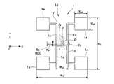
- FIG. 3 is a schematic plan view showing an example of a patch antenna of the antenna device of the present embodiment.
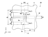
- FIG. 4 is a schematic plan view showing an example of the opening shape of the slot used in the antenna device of the present embodiment.
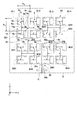
- FIG. 5 is a schematic plan view showing an example of the wiring pattern of the feed conductor of the antenna device of the present embodiment.
- FIG. 6 is a schematic plan view showing an example of a wiring pattern of a feeding conductor for feeding power to the antenna block in the antenna device of the present embodiment.
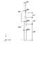
- FIG. 7 is a schematic plan view showing an example of the impedance matching portion on the base end side of the feed conductor in the antenna device of the present embodiment.
- the antenna device 20 of the present embodiment shown in FIG. 1 includes a planar antenna of an electromagnetic coupling feed system.
- the antenna device 20 can be used as an antenna device in communication in the IoT (Internet of Things) field or in high-speed wireless communication such as WiGig (Wireless Gigabit).
- IoT Internet of Things
- WiGig Wireless Gigabit
- the patch antenna 1, the first dielectric layer 2, the ground conductor plate 4, the second dielectric layer 5, and the feeding conductor 60 are stacked in this order. ing.
- the stacking direction is referred to as the Z-axis direction
- biaxial directions orthogonal to the Z-axis direction and orthogonal to each other will be referred to as an X-axis direction (second direction) and a Y-axis direction (first direction).
- the coordinate system here is right-handed.
- the patch antenna 1 is patterned on a first surface 2a (first surface) of a first dielectric layer 2 described later based on a predetermined arrangement pattern.
- the normal direction of the patch antenna 1 and the first surface 2a is the Z-axis direction.
- the patch antenna 1 is a flat antenna electromagnetically coupled and fed from a feed conductor 60 described later.
- a plurality of patch antennas 1 are, for example, arranged in the form of a square grid arranged in the X-axis direction and the Y-axis direction.
- each patch antenna 1 includes, as an example, four radiating elements 1 a and a divided circuit pattern 1 d which is a divider for arraying the respective radiating elements 1 a.
- Each of the radiation elements 1a is formed in a rectangular shape having sides extending in the X-axis direction and the Y-axis direction. Each of the radiation elements 1a is arranged in a substantially square lattice rectangular grid arranged in the X axis direction and the Y axis direction.
- the divided circuit pattern 1 d includes an electrode portion 1 b for electromagnetic coupling, and four wiring portions 1 c that electrically connect the electrode portion 1 b and the radiation elements 1 a to each other.
- the electrode portion 1b is formed in a rectangular shape extending in the X-axis direction centering on a point P which is an intersection point of diagonal lines connecting centers of arrangement positions of the radiation elements 1a.
- the feeding point in the electrode portion 1b is formed at the center of the electrode portion 1b.
- Each wiring portion 1c extends from the side portion in the Y-axis direction at the four corner portions of the electrode portion 1b toward the radiation element 1a connected thereto. Specifically, each wiring portion 1c extends in the Y-axis direction toward the radiation element 1a to which each wiring portion 1c is connected, and then a position facing the central portion of the side portion in the X-axis direction of the radiation element 1a to which each is connected It bends at a right angle so as to go in the X-axis direction. The path lengths of the wiring portions 1c are equal to one another. At the corner of the bent portion in each wiring portion 1c, a chamfered portion 1f which intersects the X axis at 45 degrees is formed.
- each patch antenna 1 having such a configuration is disposed at a corner of a rectangular area having a width W X in the X-axis direction and a width W Y in the Y-axis direction.
- W x and W y may be 4.4 mm and 4.52 mm, respectively.
- the width W aX in the X-axis direction of the radiating elements 1a, the width in the Y-axis direction W aY, respectively, 1.15 mm may be 1.15 mm.
- the width W bX in the X-axis direction of the electrode portion 1 b and the width W bY in the Y-axis direction may be 0.8 mm or 0.4 mm, respectively.
- the line width of each wiring portion 1c may be 0.13 mm.
- the quarter effective length (hereinafter simply referred to as the effective length) of such a patch antenna 1 is 1.15 mm.
- the patch antenna 1 is formed of, for example, a metal material such as copper.
- the impedance from the point P to each radiation element 1 a is set to an impedance such that the current direction in each radiation element 1 a is the same.
- the current direction in each radiation element 1a flows in the same direction in the X-axis direction which is a direction parallel to the tip line 6e described later as a whole.
- the first dielectric layer 2 is a flat member having a dielectric constant and a layer thickness defined in accordance with the required radiation characteristics.
- the first dielectric layer 2 may be a single layer dielectric, or a plurality of dielectrics may be bonded. Whether to use a single layer or multiple layers may be determined in consideration of, for example, the material cost.
- the example shown in FIG. 2 shows an example in which the dielectric 2A having a certain thickness is formed by being bonded by the resin adhesive layer 2B which is a dielectric.
- a second surface 2b (second surface), which is a surface opposite to the first surface 2a in the first dielectric layer 2, is formed of a resin adhesive layer 2B.
- the resin adhesive layer 2B constituting the second surface 2b joins a ground conductor plate 4 described later.
- the first dielectric layer 2 is composed of a plurality of layers, it is easy to change the dielectric constant and the layer thickness of the first dielectric layer 2. This makes it easier to set the impedance of each part to a predetermined value.
- the ground conductor plate 4 is a plate member of a conductor in which slots 7 are formed at positions facing the patch antennas 1.
- the ground conductor plate 4 is grounded.
- the ground conductor plate 4 is fixed to the first dielectric layer 2 via the resin adhesive layer 2B constituting the second surface 2b.
- the slot 7 is a nonconductor in the ground conductor plate 4. As shown in FIGS. 3 and 4, the slot 7 extends in the Y-axis direction which is the first direction.
- the opening shape of the slot 7 is a shape capable of achieving impedance matching between the impedance of the patch antenna 1 and a feeding conductor 60 described later.
- the slot 7 in this embodiment is H-shaped as viewed from the Z-axis direction, as shown in FIG. Specifically, the slot 7 has a rectangular first opening 7a and second openings 7b formed at both ends in the longitudinal direction (first direction) of the first opening 7a, Equipped with As shown in FIG.
- the center (centre) of the slot 7 is arranged to overlap the point P which is the center (centre) of the electrode portion 1 b of the patch antenna 1. Therefore, when viewed from the Z-axis direction, the slot 7 is orthogonal to the centers of the electrode portion 1b and the electrode portion 1b, and traverses the electrode portion 1b in the Y-axis direction.
- the first opening 7a constitutes a passing signal portion through which a signal passes.
- Each second opening 7 b is an opening that increases the impedance at both ends of the passing signal portion. More preferably, the length d3 of the slot 7 in the longitudinal direction (first direction) is adjusted to the effective length of the patch antenna 1.
- the width W2 in the short direction of the first opening 7a is more preferably 0.75 mm, for example, in order to set the coupling impedance to 112 ⁇ .
- W2 is more preferably 0.2 mm.
- each second opening 7b widens from the width W2 in the short direction of the first opening 7a in order to form an impedance larger than the coupling impedance by the first opening 7a.
- each second opening 7b is a rectangle having a length d2 in the Y-axis direction and a width W3 in the X-axis direction (where W3> W2).
- d2 and W3 may be 0.2 mm and 0.4 mm, respectively.
- the coupling impedance of the electromagnetic coupling feeding portion is 112 ⁇ at the central portion of the electrode portion 1 b.
- the second dielectric layer 5 includes a ground conductor plate 4 and a feeding conductor 60 described later so as to perform electromagnetic coupling feeding to the patch antenna 1 from the feeding conductor 60 described later and the slot 7. It is provided to be separated by a fixed insulation distance. For this reason, the ground conductor plate 4 is disposed on the first surface 5 a of the second dielectric layer 5, and a feeding conductor 60 described later is disposed on the second surface 5 b of the second dielectric layer 5. It is done.
- the relative permittivity ⁇ r of the second dielectric layer 5 is preferably as small as possible.
- the relative dielectric constant ⁇ r of the second dielectric layer 5 is more preferably 1 or more and 2.5 or less.
- the layer thickness of the second dielectric layer 5 is more preferably 130 ⁇ m.
- quartz glass may be used as a material of the second dielectric layer 5.
- the quartz glass may be bonded to the ground conductor plate 4 by an adhesive sheet which is a dielectric. The thicknesses of the quartz glass and the adhesive sheet may be set in accordance with the respective relative dielectric constants.
- the feed conductor 60 is patterned on the second surface 5 b of the second dielectric layer 5.
- the feed conductor 60 can be electrically connected to an external circuit (not shown) via a connection path having a predetermined impedance.
- the feed conductor 60 includes a first block wiring portion 6, a second block wiring portion 16, a third block wiring portion 26, and a proximal end wiring portion 36.
- the first block wiring unit 6 is a first power supply that simultaneously feeds each patch antenna 1 of the antenna block with 2 ⁇ 2 patch antennas 1 adjacent to each other in the X-axis direction and the Y-axis direction as one antenna block. It is a wiring pattern which forms a block.
- the patch antennas 1 are arranged in a square grid of 8 ⁇ 8
- J 1,..., 4).
- the subscript i represents the arrangement order in the Y-axis direction, and means that the arrangement position shifts in the Y-axis negative direction as i increases from one.
- the subscript j represents the arrangement order in the X-axis direction, and means that the arrangement position deviates in the positive X-axis direction as j increases from one.
- Arrangement pitch P X in the X-axis direction of each block Bij, the arrangement pitch P Y in the Y-axis direction, in the present embodiment, both are 14 mm. Therefore, four first block wiring portions 6 are arranged at the arrangement pitch P X in the X axis direction according to the arrangement of the blocks Bij in the X axis direction, and the arrangement pitch P in the Y axis direction according to the arrangement in the Y axis direction. Four are arranged in Y.
- the configuration of the first block wiring unit 6 in each block Bij is the same in all cases, and therefore, an example of the first block wiring unit 6 corresponding to the block B11 shown in FIG. 5 will be described.
- Four tips formed on the tip of the first block wiring portion 6 so as to overlap with the four slots 7 corresponding to the block B 11 and the respective electrode portions 1 b of the four patch antennas 1 when viewed from the Z-axis direction A line 6e (tip) is formed.
- Each tip line 6 e is a linear conductor that constitutes the open end of the feed conductor 60.
- each tip end line 6 e extends in the X axis direction, passing through the longitudinal center of the first opening 7 a of each slot 7 as viewed from the Z axis direction. . Therefore, when viewed from the Z-axis direction, the tip end line 6e crosses the first opening 7a so as to be orthogonal to the first opening 7a.
- the line width W1 of the tip line 6e is such that a very wide line width leads to more losses and radiation, and a very thin line width makes it difficult to manufacture, thus minimizing production and back radiation It has been decided as such.
- the line width W1 of the tip end line 6e may be 0.1 mm. As shown in FIG.
- the length (stub length) from the central axis O of the first opening 7 a to the tip 6 f of the tip track 6 e is ds.
- the stub length ds is made equal to the length d1 of the first opening 7a.
- the stub length ds is 0.75 mm.
- each of the tip lines 6e is a first line 6d (line) extending in the Y-axis direction at the end where the two tip lines 6e adjacent in the Y-axis direction are opposite to the tip 6f.
- the line width of each first line 6d is equal to the line width W1 of the tip line 6e.
- the two first lines 6d adjacent to each other in the X-axis direction are connected to each other by a second line 6c (a linear wiring portion) extending in the X-axis direction at a position where each longitudinal length is equally divided.
- the line width of each second line 6c is equal to the line width W1 of the tip end line 6e except for both ends in the longitudinal direction.
- the first line 6 d and the second line 6 c are connected in a T shape orthogonal to each other.
- the first line 6d is a branch line when viewed from the second line 6c, and the middle point in the longitudinal direction of the first line 6d is a branch point.
- the "midpoint" of the line means the "longitudinal midpoint of the line”.
- an impedance matching portion 6b is formed whose line width is widened stepwise from W1 as it goes from the center of the second line 6c to each branch point.
- the impedance matching unit 6b in the present embodiment performs impedance matching with the second line 6c at the branch point of the first line 6d.
- the line width of the impedance matching portion 6b is widened in three steps as W11, W12, and W13 (where W11 ⁇ W12 ⁇ W13) from the middle portion to the end portion of the second line 6c.
- the length of each portion of the line widths W11, W12, and W13 is L11, L12, and L13.
- the line widths W11, W12, and W13 are 0.12 mm, 0.22 mm, and 0.3 mm, respectively.
- the impedance of each portion of the line width W11, W12, and W13 is 96 ⁇ , 70 ⁇ , and 58 ⁇ , respectively.
- the impedance gradually changes from the main body to the branch point of the first line 6d, such as 112 ⁇ , 96 ⁇ , 70 ⁇ , and 58 ⁇ , and is matched with the impedance 56 ⁇ of the branch point.
- the amount of change in impedance by the impedance matching unit 6b is 16 ⁇ , 26 ⁇ , and 12 ⁇ for each of the line width change portions toward the branch point.
- the frequency band used by the antenna device 20 is in the 60 GHz band
- the amount of change in impedance in the line width change portion in the impedance matching portion 6b is 50 ⁇ or less
- the branch point Return loss due to current reflection in it is more preferable if the amount of change in impedance at the change in line width is 30 ⁇ or less.
- the number of stages of the widening is three.
- each tip line 6e extends from the first line 6d in the positive X-axis direction. For this reason, the current distributed to each of the tip end lines 6e flows in the same phase and in the same direction.
- Such tip lines 6e have impedance matching with the slots 7 facing each other.
- the second block wiring section 16 electrically connects the first block wiring sections 6 in the four blocks Bij adjacent to each other and arranged in a square lattice.
- the second block wiring portion 16 is a substantially H-shaped wiring pattern which forms a second feeding block for feeding the four patch antennas 1 forming the block Bij together in units of four blocks.
- the second block wiring portion 16 corresponds to each first block wiring portion 6 corresponding to the blocks B11, B12, B21 and B22, and each first block wiring portion corresponding to the blocks B13, B14, B23 and B24.
- the second block wiring section 16 includes a first line 16a (linear wiring section), a second line 16b (linear wiring section), and a third line 16c (linear wiring section).
- the first line 16a includes a middle point of the second line 6c of the first block wiring section 6 corresponding to the block B11 and a middle point of the second line 6c of the first block wiring section 6 corresponding to the block B21. Electrically connect in the Y-axis direction. For example, as shown in FIG.
- the end of the first line 16a connected to the second line 6c of the first block wiring portion 6 corresponding to the block B11 is bent in the negative direction of the X axis, and then the Y axis direction
- the second line 6c is connected to the second line 6c at a position opposed to the middle point of the second line 6c via the impedance matching portion 6b extending in the direction.
- the second line 6c is a branch line when viewed from the first line 16a, and the middle point of the second line 6c is a branch point.
- the second line 16b includes a middle point of the second line 6c of the first block wiring section 6 corresponding to the block B12 and a middle point of the second line 6c of the first block wiring section 6 corresponding to the block B22. Electrically connect in the Y-axis direction.
- the shape and arrangement of the second line 16b are the same as the first line 16a except that the connected second line 6c is different.
- the third line 16c electrically connects the middle point of the first line 16a and the middle point of the second line 16b via the impedance matching unit 6b.
- the third line 16c is formed in a linear shape extending in the X-axis direction.
- the first line 16a and the second line 16b are branch lines when viewed from the third line 16c, and the middle points of the first line 16a and the second line 16b are branch points.
- the line widths of the main portions of the first line 16a, the second line 16b, and the lines of the third line 16c excluding the impedance matching portion 6b are all W1. For this reason, at each branch point of the second block wiring portion 16, impedance matching is performed by the impedance matching portion 6b as in the case of the first block wiring portion 6 described above.
- the third block wiring unit 26 electrically connects the four second feed blocks electrically connected by the second block wiring units 16 to each other.
- the third block wiring portion 26 is a substantially H-shaped wiring pattern that forms a third power feeding block that feeds power to the four second power feeding blocks collectively.
- the third block wiring section 26 includes a second block wiring section 16 connected to the first block wiring sections 6 corresponding to the blocks B11, B12, B21 and B22, and the blocks B13, B14, B23 and B24.
- the third block wiring section 26 includes a first line 26 a (linear wiring section), a second line 26 b (linear wiring section), and a third line 26 c (linear wiring section).
- the first line 26a is located between the middle point of the third line 16c extending in the X-axis direction and interposed between the blocks B11 and B12 and the blocks B21 and B22, the blocks B31 and B32, and the blocks B41 and B42.
- the middle point of the third line 16c extending in the X-axis direction are electrically connected to each other through the impedance matching portion 6b.
- the first line 26a is formed in a straight line extending in the Y-axis direction.
- Each third line 16c to which the first line 26a is connected is a branch line when viewed from the first line 26a, and the middle point of the third line 16c is a branch point.
- the second line 26b is located between the middle point of the third line 16c extending in the X-axis direction and interposed between the blocks B13 and B14 and the blocks B23 and B24, the blocks B33 and B34, and the blocks B43 and B44. And the middle point of the third line 16c extending in the X-axis direction are electrically connected to each other through the impedance matching portion 6b.
- the second line 26 b is formed in a linear shape extending in the Y-axis direction.
- Each third line 16c to which the second line 26b is connected is a branch line when viewed from the second line 26b, and the middle point of the third line 16c is a branch point.
- the third line 26c electrically connects the middle point of the first line 26a and the middle point of the second line 26b via the impedance matching unit 6b.
- the third line 26c is formed in a linear shape extending in the X-axis direction.
- the first line 26a and the second line 26b are branch lines when viewed from the third line 26c, and the middle points of the first line 26a and the second line 26b are branch points.
- the line widths of the main portions of the first line 26a, the second line 26b, and the third line 26c excluding the impedance matching portions 6b are all W1. For this reason, at each branch point of the third block wiring section 26, impedance matching is performed by the impedance matching section 6b as in the case of the first block wiring section 6 described above.
- the base end wiring portion 36 is extended in the Y-axis direction between the blocks B32 and B42 and the blocks B33 and B43 in order to electrically connect the outside of the antenna device 20 to the third block wiring portion 26.
- a substantially straight base end line 36a (a linear wiring portion) is provided.
- the illustrated upper end of the base end line 36 a is connected to the third line 26 c of the third block wiring section 26.
- the upper end of the base end line 36a is bent in the negative X-axis direction, and then the third end of the base line 36a is extended through the impedance matching portion 6b extending in the Y-axis direction. It is connected to the middle point of the line 26c.
- the third line 26c is a branch line when viewed from the base end line 36a, and the middle point of the third line 26c is a branch point.
- An impedance matching portion 36b is formed at the lower end portion of the base end line 36a in the drawing.
- the impedance matching portion 36 b is provided at the base end of the feed conductor 60 and is a feed source of the feed conductor 60.
- a coaxial cable for feeding of the impedance 50 ⁇ (not shown) is electrically connected to the impedance matching unit 36b.
- the line width of the main body excluding the impedance matching portions 6b and 36b is W1 as in the case of the third line 26c.
- the impedance matching portion 36b has three stages of line widths W21, W22, W23 (where W21 ⁇ W22 ⁇ W23) from the middle portion of the base end line 36a toward the lower end in the figure. Widening.
- the lengths of respective portions of the line widths W21, W22, and W23 are L21, L22, and L23.
- the impedance matching portion 36b at the base end of the feeding conductor 60 changes in impedance in the line width changing portion It is more preferable that the amount is 50 ⁇ or less, and the change in impedance of the widening stage closest to the end at the proximal end is 30 ⁇ or less. In this case, the return loss due to the current reflection at the base end of the feeding conductor 60 is better suppressed.
- the line widths W21, W22, and W23 are 0.18 mm, 0.28 mm, and 0.38 mm, respectively.
- the impedance of each portion of the line widths W21, W22, and W23 is 78 ⁇ , 60 ⁇ , and 50 ⁇ , respectively.
- the lengths L21, L22 and L23 in the impedance matching portion 36b are 1 mm, 2 mm and 5 mm, respectively.
- the line width of the impedance matching section 36b is expanded in three stages, and the impedance is 112 ⁇ , 78 ⁇ , 60 ⁇ , 50 ⁇ , etc., from the main body of the base end line 36a toward the feed source. It changes gradually in multiple steps and is matched with the impedance 50 ⁇ of the coaxial cable.
- the amount of change in impedance by the impedance matching unit 36b is 42 ⁇ , 18 ⁇ , and 10 ⁇ for each of the line width change portions toward the power supply source.
- the antenna device 20 having such a configuration is manufactured, for example, as follows. First, conductor films are formed on the first surface 5a and the second surface 5b of the second dielectric layer 5, respectively, and then the ground conductor plate 4 and the feeding conductor 60 are respectively patterned by etching or the like. Furthermore, the first dielectric layer 2 to which the dielectric 2A is bonded is bonded onto the ground conductor plate 4. Thereafter, a conductor film is formed on the first surface 2 a of the first dielectric layer 2, and the patch antenna 1 is patterned by, for example, etching or the like. After the patch antenna 1 is patterned on the first dielectric layer 2, the first dielectric layer 2 and the ground conductor plate 4 may be bonded.
- FIG. 8A is a simulation diagram of an example for explaining the wiring pattern of the feed conductor in the antenna device of the present embodiment.
- FIG. 8B is a simulation diagram of a comparative example.
- each of the T-shaped branch wiring patterns of the feeding conductor 60 when power is supplied from the impedance matching portion 36b of the feeding conductor 60, each of the T-shaped branch wiring patterns of the feeding conductor 60 The current is equally distributed to the tip end line 6e.
- the line lengths from the feeding source to each tip line 6e are equal to each other, and the direction of the tip of the tip line 6e is uniform in the X-axis positive direction.
- the currents of the same phase are electromagnetically coupled and fed by the same amount in the same direction.
- the coupling impedance in the electromagnetic coupling feed from the tip line 6e to the electrode portion 1b of the patch antenna 1 also needs to be matched.
- the arrangement and shape of the first opening 7a of the slot 7 in the ground conductor plate 4 are optimized, the second opening 7b is provided in the slot 7, and the tip end line 6e
- the coupling impedance is matched by optimizing the stub length ds.
- high impedance regions are formed outside the both ends of the first opening 7a. Therefore, in the first opening 7a, the signal passes efficiently, so that the reflection loss as a whole is reduced.
- the current fed to the electrode portion 1 b is equally divided into the respective radiation elements 1 a in the same phase by the divided circuit pattern 1 d of the patch antenna 1. In this manner, in the antenna device 20, currents flow through the respective radiation elements 1a in the same phase and in substantially the same direction. For this reason, the gain of the radio wave radiated from each patch antenna 1 becomes good.
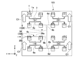
- FIG. 8A The structure of the antenna apparatus 101 of an Example and simulation result are shown in figure by FIG. 8A.
- FIG. 8A is a schematic view, a part of the shape is simplified.
- the 64 patch antennas 1 in the antenna device 20 are replaced with four patch antennas 1, and the first block wiring portion 6 and the base end wiring portion are substituted for the feeding conductors 60 correspondingly.
- a feed conductor 106 is provided.
- the other configuration is the same as that of the antenna device 20.
- the proximal end wiring portion 36 in the antenna device 101 extends in the Y-axis direction, and is connected to the middle point of the second line 6 c.
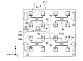
- the structure of the antenna apparatus 111 of a comparative example and simulation result are shown in figure by FIG. 8B. However, since FIG. 8B is a schematic view, a part of the shape is simplified.
- the antenna device 111 includes a feeding conductor 126 instead of the feeding conductor 106 of the antenna device 101.
- the feeding conductor 126 includes a first block wiring portion 116 instead of the first block wiring portion 6 of the feeding conductor 106.
- differences from the antenna device 101 will be mainly described.
- the first lines 6d and the respective tip lines 6e for feeding the two patch antennas 1 in the lower portion of the drawing are inverted in the X-axis direction with respect to the pattern of the first block wiring portion 6.
- the point differs in that the inverted first line 6d and the first line 6d at the top of the figure are connected by a second line 116c having impedance matching portions 6b at both ends.
- the second line 116c has a line length shorter than that of the second line 6c.
- the base end wiring portion 36 in the feed conductor 126 is formed at a position facing the middle point of the second line 116 c, and is translated in the positive X-axis direction relative to the base end wiring portion 36 in the feed conductor 106. There is.
- each patch antenna 1 The electric current and radiation pattern which flow into each patch antenna 1 at the time of supplying electric power from proximal end wiring part 36 to antenna apparatus 101 and 111 of such composition were simulated, respectively.
- the current direction in each of the radiation elements 1a is aligned in a substantially fixed direction (the X-axis positive direction in the illustrated example) as indicated by a solid arrow in FIG. 8A.
- the antenna device 111 as shown in FIG. 8B, the current directions of the radiation elements 1a of the two lower patch antennas 1 shown in the figure are the same as those of the antenna device 101.
- each radiation element 1 a was opposite to that of the antenna device 101.
- the direction of the current flowing through each patch antenna 1 as a whole is opposite to the direction of the tip of the tip line 6e.
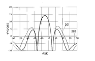
- FIG. 9A is a graph showing the radiation pattern of the example
- FIG. 9B is a graph showing the radiation pattern of the comparative example.
- the horizontal axis is the elevation angle ⁇ (degrees)
- the vertical axis is the gain (dBi).
- 9A and 9B broken lines (curves 201 and 203) represent total gains in the XZ plane
- solid lines represent total gains in the YZ plane.
- the XZ plane is an electric plane (E plane)
- the YZ plane is a magnetic plane (H plane).
- FIG. 10 is a graph showing the total gain in the antenna device of the present embodiment.
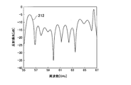
- FIG. 11 is a graph showing the reflection loss (S11) in the antenna device of the present embodiment.
- FIG. 10 shows simulation results of all gains in the XZ plane and the YZ plane.
- the horizontal axis is the elevation angle ⁇ (degrees), and the vertical axis is the gain (dBi).
- a curve 210 (broken line) represents the total gain in the XZ plane
- a curve 211 (solid line) represents the total gain in the YZ plane.
- the XZ plane is an electric plane (E plane)
- the YZ plane is a magnetic plane (H plane).
- good total gain is obtained in both the XZ plane and the YZ plane in the range of the elevation angle of 0 ° to ⁇ 4 °.
- FIG. 11 shows the frequency characteristics of the reflection loss (S11).
- the horizontal axis is frequency (GHz) and the vertical axis is reflection loss (dB).
- the reflection loss is ⁇ 10 dB or less. For this reason, the antenna device 20 has a good return loss characteristic in a 60 GHz band wireless communication application.
- the antenna device 20 of the present embodiment is excellent in the efficiency of design work because it is easy to make design changes according to other specifications.
- the arrangement of the patch antenna 1 and the radiation element 1a is a square lattice and a substantially square lattice, respectively, and the tip line 6e is arranged in a predetermined positional relationship with each patch antenna 1 when viewed from the normal direction. .
- the linear wiring portions except for the tip line 6e may be provided to extend in the X-axis direction or the Y-axis direction in the region between the adjacent patch antennas 1, the arrangement space is insufficient even if the wiring pattern increases. I have nothing to do.
- the line width of the main body is fixed, and a predetermined impedance matching portion is formed only at the end connected to the branch point, whereby impedance matching with less return loss is performed. For this reason, the design of each linear wiring portion is easy, and the antenna can be miniaturized.
- the antenna device 20 of the present embodiment efficient design is possible, and the gain is good.
- the number of patch antennas 1 is 64 and 4 in the above embodiment, the number of patch antennas 1 is 2 N (where N is an integer of 2 or more). For example, 64 or 4 are not limited.
- the four radiating elements 1a are arranged in a rectangular grid of substantially square grid to form the patch antenna 1, and the patch antenna 1 is further arranged in a square grid.
- the four radiation elements 1a may be arranged in a rectangular grid shape in which the arrangement pitch in the first direction and the second direction is largely different.
- the patch antenna 1 is not limited to the square lattice arrangement, and may be arranged in a rectangular lattice arrangement.
Landscapes
- Physics & Mathematics (AREA)
- Electromagnetism (AREA)
- Variable-Direction Aerials And Aerial Arrays (AREA)
- Waveguide Aerials (AREA)
- Details Of Aerials (AREA)
Abstract
L'invention concerne une antenne à plaque comprenant : quatre éléments de rayonnement agencés selon un motif de réseau rectangulaire sur quatre côtés ayant un point d'alimentation électrique en tant que centre de ceux-ci ; et une section de câblage qui connecte électriquement, en phase, chaque élément de rayonnement et le point d'alimentation électrique. L'antenne à plaque a une puissance fournie à celle-ci par un conducteur d'alimentation électrique linéaire agencé à une position croisant une fente formée dans une plaque conductrice de masse. Le conducteur d'alimentation électrique a un motif de ramification répétitif par lequel une pluralité de sections de câblage linéaires sont couplées en forme de T, orthogonales les unes par rapport aux autre, à un total de 2N – 1 points de ramification jusqu'à ce que lesdites sections de câblage linéaires se connectent d'une section d'extrémité de base à une section de pointe. Chacune des sections de pointe est incurvée dans la même direction dans la seconde direction, à partir d'une extrémité des sections de câblage linéaires auxquelles les sections de pointe sont connectées.
Priority Applications (3)
| Application Number | Priority Date | Filing Date | Title |
|---|---|---|---|
| US16/643,913 US11108166B2 (en) | 2017-09-21 | 2018-09-12 | Antenna device |
| EP18858879.2A EP3686998A4 (fr) | 2017-09-21 | 2018-09-12 | Dispositif d'antenne |
| CA3074670A CA3074670A1 (fr) | 2017-09-21 | 2018-09-12 | Dispositif d'antenne |
Applications Claiming Priority (2)
| Application Number | Priority Date | Filing Date | Title |
|---|---|---|---|
| JP2017181339A JP2019057832A (ja) | 2017-09-21 | 2017-09-21 | アンテナ装置 |
| JP2017-181339 | 2017-09-21 |
Publications (1)
| Publication Number | Publication Date |
|---|---|
| WO2019059062A1 true WO2019059062A1 (fr) | 2019-03-28 |
Family
ID=65809842
Family Applications (1)
| Application Number | Title | Priority Date | Filing Date |
|---|---|---|---|
| PCT/JP2018/033784 Ceased WO2019059062A1 (fr) | 2017-09-21 | 2018-09-12 | Dispositif d'antenne |
Country Status (5)
| Country | Link |
|---|---|
| US (1) | US11108166B2 (fr) |
| EP (1) | EP3686998A4 (fr) |
| JP (1) | JP2019057832A (fr) |
| CA (1) | CA3074670A1 (fr) |
| WO (1) | WO2019059062A1 (fr) |
Families Citing this family (2)
| Publication number | Priority date | Publication date | Assignee | Title |
|---|---|---|---|---|
| CN109103605A (zh) * | 2018-08-07 | 2018-12-28 | 北京凌波微步信息技术有限公司 | 一种采用倒置微带缝隙波导馈电的阵列天线 |
| CN112290222B (zh) * | 2020-09-27 | 2021-10-08 | 南京大学 | 一种可编程各向异性编码超表面 |
Citations (7)
| Publication number | Priority date | Publication date | Assignee | Title |
|---|---|---|---|---|
| JPS6474717A (en) | 1987-09-17 | 1989-03-20 | Matsushita Electric Industrial Co Ltd | Formation of thin film |
| JPH03101507A (ja) * | 1989-09-14 | 1991-04-26 | Yagi Antenna Co Ltd | 平面アンテナ |
| JPH11266118A (ja) * | 1998-03-17 | 1999-09-28 | Matsushita Electric Ind Co Ltd | パッチアレイアンテナ |
| JP2004200774A (ja) * | 2002-12-16 | 2004-07-15 | Alps Electric Co Ltd | 円偏波平面アンテナ |
| US20090128435A1 (en) * | 2007-11-16 | 2009-05-21 | Smartant Telecom Co., Ltd. | Slot-coupled microstrip antenna |
| US20160380362A1 (en) * | 2014-03-12 | 2016-12-29 | Huawei Technologies Co., Ltd. | Array antenna |
| JP2017181339A (ja) | 2016-03-31 | 2017-10-05 | 大日本印刷株式会社 | 応力発光パネル |
Family Cites Families (11)
| Publication number | Priority date | Publication date | Assignee | Title |
|---|---|---|---|---|
| JPH0355904A (ja) | 1989-07-25 | 1991-03-11 | Toshiba Corp | 平面アンテナ |
| JP3004439B2 (ja) | 1992-01-17 | 2000-01-31 | 日立化成工業株式会社 | 平面アンテナ |
| JPH1174717A (ja) | 1997-06-23 | 1999-03-16 | Nec Corp | フェーズドアレーアンテナ装置 |
| JPWO2010013610A1 (ja) * | 2008-07-30 | 2012-01-12 | 日本電気株式会社 | 平面アンテナ |
| JP5408160B2 (ja) * | 2011-03-09 | 2014-02-05 | 株式会社村田製作所 | 水平方向放射アンテナ |
| JP5429215B2 (ja) * | 2011-03-09 | 2014-02-26 | 株式会社村田製作所 | 水平方向放射アンテナ |
| JP5773071B2 (ja) * | 2012-04-02 | 2015-09-02 | 株式会社村田製作所 | アンテナ装置 |
| WO2015168598A1 (fr) | 2014-05-02 | 2015-11-05 | AMI Research & Development, LLC | Réseau de balayage à onde progressive diélectrique quasi tem |
| WO2018230475A1 (fr) * | 2017-06-14 | 2018-12-20 | 株式会社村田製作所 | Module d'antenne et dispositif de communication |
| JP6341399B1 (ja) * | 2018-03-14 | 2018-06-13 | パナソニックIpマネジメント株式会社 | アンテナ装置 |
| JP6705577B1 (ja) * | 2018-08-20 | 2020-06-03 | 株式会社村田製作所 | アンテナ素子、アンテナモジュールおよび通信装置 |
-
2017
- 2017-09-21 JP JP2017181339A patent/JP2019057832A/ja active Pending
-
2018
- 2018-09-12 US US16/643,913 patent/US11108166B2/en active Active
- 2018-09-12 EP EP18858879.2A patent/EP3686998A4/fr not_active Withdrawn
- 2018-09-12 CA CA3074670A patent/CA3074670A1/fr not_active Abandoned
- 2018-09-12 WO PCT/JP2018/033784 patent/WO2019059062A1/fr not_active Ceased
Patent Citations (7)
| Publication number | Priority date | Publication date | Assignee | Title |
|---|---|---|---|---|
| JPS6474717A (en) | 1987-09-17 | 1989-03-20 | Matsushita Electric Industrial Co Ltd | Formation of thin film |
| JPH03101507A (ja) * | 1989-09-14 | 1991-04-26 | Yagi Antenna Co Ltd | 平面アンテナ |
| JPH11266118A (ja) * | 1998-03-17 | 1999-09-28 | Matsushita Electric Ind Co Ltd | パッチアレイアンテナ |
| JP2004200774A (ja) * | 2002-12-16 | 2004-07-15 | Alps Electric Co Ltd | 円偏波平面アンテナ |
| US20090128435A1 (en) * | 2007-11-16 | 2009-05-21 | Smartant Telecom Co., Ltd. | Slot-coupled microstrip antenna |
| US20160380362A1 (en) * | 2014-03-12 | 2016-12-29 | Huawei Technologies Co., Ltd. | Array antenna |
| JP2017181339A (ja) | 2016-03-31 | 2017-10-05 | 大日本印刷株式会社 | 応力発光パネル |
Non-Patent Citations (1)
| Title |
|---|
| See also references of EP3686998A4 |
Also Published As
| Publication number | Publication date |
|---|---|
| JP2019057832A (ja) | 2019-04-11 |
| EP3686998A4 (fr) | 2021-06-09 |
| CA3074670A1 (fr) | 2019-03-28 |
| US11108166B2 (en) | 2021-08-31 |
| EP3686998A1 (fr) | 2020-07-29 |
| US20200212595A1 (en) | 2020-07-02 |
Similar Documents
| Publication | Publication Date | Title |
|---|---|---|
| JP7077587B2 (ja) | デュアルバンドパッチアンテナ | |
| KR101982028B1 (ko) | 편파 공용 안테나 | |
| US9698487B2 (en) | Array antenna | |
| US11223132B2 (en) | Antenna device | |
| JP6788685B2 (ja) | アンテナ装置 | |
| WO2017150054A1 (fr) | Antenne réseau | |
| US10270180B2 (en) | Antenna apparatus | |
| JP4238325B2 (ja) | 多周波共用マイクロストリップアンテナ | |
| JPWO2015049816A1 (ja) | アンテナ装置 | |
| JP6690672B2 (ja) | パッチアンテナ及びこれを備えるアンテナモジュール | |
| WO2019059062A1 (fr) | Dispositif d'antenne | |
| US10957981B2 (en) | Antenna device | |
| US9130276B2 (en) | Antenna device | |
| WO2019189008A1 (fr) | Antenne | |
| WO2023095239A1 (fr) | Antenne réseau et élément d'antenne | |
| JP2019022088A (ja) | アンテナ | |
| WO2019058932A1 (fr) | Dispositif d'antenne | |
| JP5049948B2 (ja) | アンテナ装置および無線通信装置 | |
| US12316031B2 (en) | Antenna device | |
| JP6201651B2 (ja) | アンテナ装置およびアレイアンテナ装置 | |
| CN121261108A (zh) | 一种低成本双圆极化mimo贴片天线 | |
| JP2023160572A (ja) | アレイアンテナ装置 | |
| WO2021100655A1 (fr) | Antenne planaire | |
| JP2008219415A (ja) | 平面アンテナ装置 |
Legal Events
| Date | Code | Title | Description |
|---|---|---|---|
| 121 | Ep: the epo has been informed by wipo that ep was designated in this application |
Ref document number: 18858879 Country of ref document: EP Kind code of ref document: A1 |
|
| ENP | Entry into the national phase |
Ref document number: 3074670 Country of ref document: CA |
|
| NENP | Non-entry into the national phase |
Ref country code: DE |
|
| ENP | Entry into the national phase |
Ref document number: 2018858879 Country of ref document: EP Effective date: 20200421 |