WO2019092982A1 - Dispositif de commande électronique, système embarqué et dispositif d'alimentation électrique - Google Patents
Dispositif de commande électronique, système embarqué et dispositif d'alimentation électrique Download PDFInfo
- Publication number
- WO2019092982A1 WO2019092982A1 PCT/JP2018/033927 JP2018033927W WO2019092982A1 WO 2019092982 A1 WO2019092982 A1 WO 2019092982A1 JP 2018033927 W JP2018033927 W JP 2018033927W WO 2019092982 A1 WO2019092982 A1 WO 2019092982A1
- Authority
- WO
- WIPO (PCT)
- Prior art keywords
- unit
- power supply
- signal
- generation unit
- current
- Prior art date
- Legal status (The legal status is an assumption and is not a legal conclusion. Google has not performed a legal analysis and makes no representation as to the accuracy of the status listed.)
- Ceased
Links
Images






Classifications
-
- H—ELECTRICITY
- H02—GENERATION; CONVERSION OR DISTRIBUTION OF ELECTRIC POWER
- H02M—APPARATUS FOR CONVERSION BETWEEN AC AND AC, BETWEEN AC AND DC, OR BETWEEN DC AND DC, AND FOR USE WITH MAINS OR SIMILAR POWER SUPPLY SYSTEMS; CONVERSION OF DC OR AC INPUT POWER INTO SURGE OUTPUT POWER; CONTROL OR REGULATION THEREOF
- H02M3/00—Conversion of DC power input into DC power output
- H02M3/02—Conversion of DC power input into DC power output without intermediate conversion into AC
- H02M3/04—Conversion of DC power input into DC power output without intermediate conversion into AC by static converters
- H02M3/10—Conversion of DC power input into DC power output without intermediate conversion into AC by static converters using discharge tubes with control electrode or semiconductor devices with control electrode
- H02M3/145—Conversion of DC power input into DC power output without intermediate conversion into AC by static converters using discharge tubes with control electrode or semiconductor devices with control electrode using devices of a triode or transistor type requiring continuous application of a control signal
- H02M3/155—Conversion of DC power input into DC power output without intermediate conversion into AC by static converters using discharge tubes with control electrode or semiconductor devices with control electrode using devices of a triode or transistor type requiring continuous application of a control signal using semiconductor devices only
- H02M3/156—Conversion of DC power input into DC power output without intermediate conversion into AC by static converters using discharge tubes with control electrode or semiconductor devices with control electrode using devices of a triode or transistor type requiring continuous application of a control signal using semiconductor devices only with automatic control of output voltage or current, e.g. switching regulators
-
- B—PERFORMING OPERATIONS; TRANSPORTING
- B60—VEHICLES IN GENERAL
- B60W—CONJOINT CONTROL OF VEHICLE SUB-UNITS OF DIFFERENT TYPE OR DIFFERENT FUNCTION; CONTROL SYSTEMS SPECIALLY ADAPTED FOR HYBRID VEHICLES; ROAD VEHICLE DRIVE CONTROL SYSTEMS FOR PURPOSES NOT RELATED TO THE CONTROL OF A PARTICULAR SUB-UNIT
- B60W60/00—Drive control systems specially adapted for autonomous road vehicles
- B60W60/001—Planning or execution of driving tasks
-
- H—ELECTRICITY
- H02—GENERATION; CONVERSION OR DISTRIBUTION OF ELECTRIC POWER
- H02M—APPARATUS FOR CONVERSION BETWEEN AC AND AC, BETWEEN AC AND DC, OR BETWEEN DC AND DC, AND FOR USE WITH MAINS OR SIMILAR POWER SUPPLY SYSTEMS; CONVERSION OF DC OR AC INPUT POWER INTO SURGE OUTPUT POWER; CONTROL OR REGULATION THEREOF
- H02M3/00—Conversion of DC power input into DC power output
- H02M3/02—Conversion of DC power input into DC power output without intermediate conversion into AC
- H02M3/04—Conversion of DC power input into DC power output without intermediate conversion into AC by static converters
- H02M3/10—Conversion of DC power input into DC power output without intermediate conversion into AC by static converters using discharge tubes with control electrode or semiconductor devices with control electrode
- H02M3/145—Conversion of DC power input into DC power output without intermediate conversion into AC by static converters using discharge tubes with control electrode or semiconductor devices with control electrode using devices of a triode or transistor type requiring continuous application of a control signal
- H02M3/155—Conversion of DC power input into DC power output without intermediate conversion into AC by static converters using discharge tubes with control electrode or semiconductor devices with control electrode using devices of a triode or transistor type requiring continuous application of a control signal using semiconductor devices only
- H02M3/156—Conversion of DC power input into DC power output without intermediate conversion into AC by static converters using discharge tubes with control electrode or semiconductor devices with control electrode using devices of a triode or transistor type requiring continuous application of a control signal using semiconductor devices only with automatic control of output voltage or current, e.g. switching regulators
- H02M3/157—Conversion of DC power input into DC power output without intermediate conversion into AC by static converters using discharge tubes with control electrode or semiconductor devices with control electrode using devices of a triode or transistor type requiring continuous application of a control signal using semiconductor devices only with automatic control of output voltage or current, e.g. switching regulators with digital control
-
- H—ELECTRICITY
- H02—GENERATION; CONVERSION OR DISTRIBUTION OF ELECTRIC POWER
- H02M—APPARATUS FOR CONVERSION BETWEEN AC AND AC, BETWEEN AC AND DC, OR BETWEEN DC AND DC, AND FOR USE WITH MAINS OR SIMILAR POWER SUPPLY SYSTEMS; CONVERSION OF DC OR AC INPUT POWER INTO SURGE OUTPUT POWER; CONTROL OR REGULATION THEREOF
- H02M3/00—Conversion of DC power input into DC power output
- H02M3/02—Conversion of DC power input into DC power output without intermediate conversion into AC
- H02M3/04—Conversion of DC power input into DC power output without intermediate conversion into AC by static converters
- H02M3/10—Conversion of DC power input into DC power output without intermediate conversion into AC by static converters using discharge tubes with control electrode or semiconductor devices with control electrode
- H02M3/145—Conversion of DC power input into DC power output without intermediate conversion into AC by static converters using discharge tubes with control electrode or semiconductor devices with control electrode using devices of a triode or transistor type requiring continuous application of a control signal
- H02M3/155—Conversion of DC power input into DC power output without intermediate conversion into AC by static converters using discharge tubes with control electrode or semiconductor devices with control electrode using devices of a triode or transistor type requiring continuous application of a control signal using semiconductor devices only
- H02M3/156—Conversion of DC power input into DC power output without intermediate conversion into AC by static converters using discharge tubes with control electrode or semiconductor devices with control electrode using devices of a triode or transistor type requiring continuous application of a control signal using semiconductor devices only with automatic control of output voltage or current, e.g. switching regulators
- H02M3/158—Conversion of DC power input into DC power output without intermediate conversion into AC by static converters using discharge tubes with control electrode or semiconductor devices with control electrode using devices of a triode or transistor type requiring continuous application of a control signal using semiconductor devices only with automatic control of output voltage or current, e.g. switching regulators including plural semiconductor devices as final control devices for a single load
-
- H—ELECTRICITY
- H02—GENERATION; CONVERSION OR DISTRIBUTION OF ELECTRIC POWER
- H02M—APPARATUS FOR CONVERSION BETWEEN AC AND AC, BETWEEN AC AND DC, OR BETWEEN DC AND DC, AND FOR USE WITH MAINS OR SIMILAR POWER SUPPLY SYSTEMS; CONVERSION OF DC OR AC INPUT POWER INTO SURGE OUTPUT POWER; CONTROL OR REGULATION THEREOF
- H02M3/00—Conversion of DC power input into DC power output
- H02M3/02—Conversion of DC power input into DC power output without intermediate conversion into AC
- H02M3/04—Conversion of DC power input into DC power output without intermediate conversion into AC by static converters
- H02M3/10—Conversion of DC power input into DC power output without intermediate conversion into AC by static converters using discharge tubes with control electrode or semiconductor devices with control electrode
- H02M3/145—Conversion of DC power input into DC power output without intermediate conversion into AC by static converters using discharge tubes with control electrode or semiconductor devices with control electrode using devices of a triode or transistor type requiring continuous application of a control signal
- H02M3/155—Conversion of DC power input into DC power output without intermediate conversion into AC by static converters using discharge tubes with control electrode or semiconductor devices with control electrode using devices of a triode or transistor type requiring continuous application of a control signal using semiconductor devices only
- H02M3/156—Conversion of DC power input into DC power output without intermediate conversion into AC by static converters using discharge tubes with control electrode or semiconductor devices with control electrode using devices of a triode or transistor type requiring continuous application of a control signal using semiconductor devices only with automatic control of output voltage or current, e.g. switching regulators
- H02M3/158—Conversion of DC power input into DC power output without intermediate conversion into AC by static converters using discharge tubes with control electrode or semiconductor devices with control electrode using devices of a triode or transistor type requiring continuous application of a control signal using semiconductor devices only with automatic control of output voltage or current, e.g. switching regulators including plural semiconductor devices as final control devices for a single load
- H02M3/1584—Conversion of DC power input into DC power output without intermediate conversion into AC by static converters using discharge tubes with control electrode or semiconductor devices with control electrode using devices of a triode or transistor type requiring continuous application of a control signal using semiconductor devices only with automatic control of output voltage or current, e.g. switching regulators including plural semiconductor devices as final control devices for a single load with a plurality of power processing stages connected in parallel
-
- B—PERFORMING OPERATIONS; TRANSPORTING
- B60—VEHICLES IN GENERAL
- B60R—VEHICLES, VEHICLE FITTINGS, OR VEHICLE PARTS, NOT OTHERWISE PROVIDED FOR
- B60R16/00—Electric or fluid circuits specially adapted for vehicles and not otherwise provided for; Arrangement of elements of electric or fluid circuits specially adapted for vehicles and not otherwise provided for
- B60R16/02—Electric or fluid circuits specially adapted for vehicles and not otherwise provided for; Arrangement of elements of electric or fluid circuits specially adapted for vehicles and not otherwise provided for electric constitutive elements
- B60R16/03—Electric or fluid circuits specially adapted for vehicles and not otherwise provided for; Arrangement of elements of electric or fluid circuits specially adapted for vehicles and not otherwise provided for electric constitutive elements for supply of electrical power to vehicle subsystems or for
-
- H—ELECTRICITY
- H02—GENERATION; CONVERSION OR DISTRIBUTION OF ELECTRIC POWER
- H02M—APPARATUS FOR CONVERSION BETWEEN AC AND AC, BETWEEN AC AND DC, OR BETWEEN DC AND DC, AND FOR USE WITH MAINS OR SIMILAR POWER SUPPLY SYSTEMS; CONVERSION OF DC OR AC INPUT POWER INTO SURGE OUTPUT POWER; CONTROL OR REGULATION THEREOF
- H02M1/00—Details of apparatus for conversion
- H02M1/0067—Converter structures employing plural converter units, other than for parallel operation of the units on a single load
- H02M1/008—Plural converter units for generating at two or more independent and non-parallel outputs, e.g. systems with plural point of load switching regulators
Definitions
- the present invention relates to an electronic control device, an in-vehicle system, and a power supply device, and more particularly to a technology effective for controlling a power supply that supplies power to a plurality of logic circuits.
- the automated driving system needs to detect vehicles, pedestrians, white lines etc. from sensor inputs such as cameras and radars and transmit them to the driver or control the brakes and steering, so that advanced recognition algorithms and multiple algorithms Simultaneous processing of
- the SoC is a combination of various logic circuits such as a CPU (Central Processing Unit) on one chip.
- CPU Central Processing Unit
- the logic circuits embedded in the SoC have their own voltage, load current, noise, sequence and transient response requirements. In particular the voltage requirements are diverse.
- the power supply circuit is often designed to meet the requirements of each logic circuit by providing a plurality of switching circuits in parallel.
- the power supply circuit configured by the switching circuit generates noise due to the switching operation. Since the power supply circuit in the electronic control unit is connected to the vehicle battery and receives power supply, noise of the power circuit may be conducted to other vehicle equipment connected to the same vehicle battery, causing malfunction or failure. Become.
- a technique for reducing such conducted noise for example, it is widely known to insert a large capacity capacitor at the input of a power supply circuit.
- a noise reduction component such as a snubber circuit or a noise filter.
- Patent Document 1 Another noise reduction method is to spread the spectrum of switching noise to reduce the noise level (see, for example, Patent Document 1).
- the technology of Patent Document 1 has a frequency changer that repeatedly outputs a frequency change pattern including a plurality of frequency values for performing switching control in a single output power supply circuit including a plurality of switching circuits in parallel.
- the switching elements are turned on and off at the switching frequency based on the frequency change pattern output from the frequency change device, and the switching frequency parameter of each element is changed when the switching noise spectrum of each switching element is superimposed.
- a multi-channel power supply circuit including a plurality of switching circuits in parallel, when switching control is performed at the same constant switching frequency for each switching circuit, large conduction noise may be generated due to the same frequency. As a result, the multi-channel power supply circuit becomes a noise source, which may cause other electronic devices to be adversely affected, such as malfunction or a malfunction.
- Patent Document 1 is applied to a multi-channel power supply circuit, it is necessary to continuously change the frequency of the oscillator that outputs the switching control signal in order to change the switching frequency parameter of each switching element. Therefore, the frequency range has to be limited, and it is considered that the electronic control device for an autonomous driving system requiring many power supply channels can not sufficiently obtain the effect of reducing the noise level.
- each output of the multi-channel power supply circuit is designed in accordance with the requirements of the logic circuit connected thereto.
- the switching frequency is a parameter that greatly affects the power efficiency and responsiveness, which is the requirement, and the frequency range is further limited.
- An object of the present invention is to provide a technique capable of reducing, at low cost, conducted noise of an input current in a power supply circuit having a plurality of channels.
- a typical electronic control device includes a power supply that supplies power to a plurality of logic circuits and a plurality of logic circuits.
- the power supply device includes a plurality of switching circuits, a transition management unit, and a clock generation unit.
- the switching circuit generates and outputs power supplies to be supplied to the plurality of logic circuits based on the switching signal.
- the transition management unit controls a plurality of switching circuits.
- the clock generation unit generates a plurality of clock signals.
- the transition management unit has a control signal generation unit and a plurality of delay units.
- the control signal generation unit generates an intermediate control signal from the clock signal generated by the clock generation unit.
- a delay unit is provided corresponding to each of the plurality of switching circuits, delays the intermediate control signal based on a command signal, and outputs the delayed intermediate control signal as the switching signal.
- the plurality of clock signals generated by the clock generation unit have different frequencies for at least one clock signal.
- the transition management unit has a transition determination unit that generates the command signal based on control information set in advance.
- the transition determination unit calculates a total value of change amounts of input currents of the plurality of switching circuits according to the command signal, and compares the calculated total value with a preset current fluctuation threshold value.
- the delay amount of the delay unit is controlled so that the compared total value becomes equal to or less than the current fluctuation threshold value.
- a highly reliable electronic control device can be provided at low cost.
- FIG. 1 is a block diagram showing an example of a configuration of an in-vehicle system according to a first embodiment. It is a block diagram which shows an example of a structure in autonomous traveling control ECU which the vehicle-mounted system of FIG. 1 has. It is explanatory drawing which shows an example of a structure in the power supply circuit which the autonomous traveling control ECU of FIG. 2 has. It is explanatory drawing which shows an example of the circuit in the switching circuit of FIG. It is explanatory drawing which shows the example of another circuit of the switching circuit of FIG. It is a block diagram which shows an example in the transition management part which the power supply circuit of FIG. 3 has. It is a flowchart which shows an example of the transition determination processing which the transition management part of FIG. 6 performs.
- FIG. 18 is an explanatory drawing showing an example of the configuration of a transition management unit according to Embodiment 2;
- FIG. 16 is a block diagram showing an example of a configuration of a power supply circuit according to a third embodiment. It is explanatory drawing which shows an example of a structure in the transition management part which the power supply circuit of FIG. 12 has.
- Embodiment 1 ⁇ Configuration example of in-vehicle system>
- FIG. 1 is a block diagram showing an example of the configuration of an in-vehicle system 10 according to the first embodiment.
- the in-vehicle system 10 is, for example, a system that controls autonomous traveling of a vehicle.
- the on-vehicle system 10 includes a camera 101, a radar 102, a vehicle position sensor 103, an automatic driving button 104, a wireless communication unit 105, an auxiliary control ECU (Electronic Control Unit) 106, a brake control ECU, and an engine.
- a control ECU 108, a power steering control ECU 109, and an autonomous traveling control ECU 201 are provided.
- the camera 101, the radar 102, and the vehicle position sensor 103 are external world recognition sensors that recognize the external world situation of the vehicle.
- the camera 101 and the radar 102 are sensors for recognizing the external world and for determining the distance to an object.
- the host vehicle position sensor 103 is a sensor that detects the host vehicle position by GPS (Global Positioning System) or the like.
- the automatic operation button 104 is a button for starting automatic operation control or changing the automatic operation mode.
- the wireless communication unit 105 which is a communication device, is connected to a wireless network (not shown) for updating the in-vehicle system by, for example, OTA (Over-The-Air).
- An autonomous travel control ECU 201 which is an electronic control unit and an autonomous travel control unit, is a vehicle travel control unit for automatic driving.
- the auxiliary control ECU 106 is an auxiliary driving vehicle traveling control device.
- the brake control ECU 107 is a control device that performs brake control of the vehicle, that is, braking force control.
- the engine control ECU 108 is a control device that controls an engine that generates a driving force of the vehicle.
- the power steering control ECU 109 is a control device that controls power steering of the vehicle.
- the camera 101, the radar 102, the vehicle position sensor 103, the automatic driving button 104, and the wireless communication unit 105 are connected to the autonomous traveling control ECU 201, respectively.
- the autonomous traveling control ECU 201 includes sensor information from the camera 101, the radar 102, and the vehicle position sensor 103, an autonomous driving control signal from the autonomous driving button 104, and autonomous traveling control processing information from the wireless communication unit 105. Update information etc. are transmitted.
- the autonomous traveling control ECU 201, the auxiliary control ECU 106, the brake control ECU 107, the engine control ECU 108, and the power steering control ECU 109 are communicably connected to each other by, for example, a CAN (Controller Area Network).
- CAN Controller Area Network
- the autonomous traveling control ECU 201 When the autonomous traveling control ECU 201 receives a request to start automatic driving from the automatic driving button 104, the autonomous traveling control ECU 201 calculates a moving route of the vehicle based on information of the outside world such as the camera 101, the radar 102, and the vehicle position sensor 103.
- the autonomous traveling control ECU 201 outputs control commands such as a brake and a driving force to the brake control ECU 107, the engine control ECU 108, and the power steering control ECU 109 so as to move the vehicle along the route described above.
- the brake control ECU 107, the engine control ECU 108, and the power steering control ECU 109 receive a control command of autonomous traveling control from the autonomous traveling control ECU 201, and output an operation signal to each control object such as an actuator.
- the autonomous traveling control ECU 201 is a main control device that outputs a control command, and the brake control ECU 107, the engine control ECU 108, and the power steering control ECU 109 control the control target according to the control command from the autonomous traveling control ECU 201. It is a sub control device.
- the auxiliary control ECU 106 is an auxiliary control device for performing automatic driving control in place of the autonomous traveling control ECU 201 when the autonomous traveling control ECU 201 is abnormal. ⁇ About the autonomous traveling control ECU>
- FIG. 2 is a block diagram showing an example of the configuration of the autonomous traveling control ECU 201 included in the on-vehicle system 10 of FIG.
- the autonomous traveling control ECU 201 includes a power supply circuit 210 and a plurality of SoCs 211 as shown in FIG.
- the power supply circuit 210 which is a power supply device, supplies power to the plurality of SoCs 211. In other words, power is supplied to the plurality of SoCs 211.
- the SoC 211 includes a CPU 212, a GPU 213, and an FPGA 214.
- the CPU 212 includes core logic 215 which is a logic circuit of the core and an input / output circuit 216 which is a logic circuit.
- the GPU 213 has core logic 217 which is a core logic circuit and an input / output circuit 218, and the FPGA 214 has a core logic 219 which is a core logic circuit and an input / output circuit 220.
- the core logics 215, 217, 219 and the input / output circuits 216, 218, 220 comprise logic circuits.
- memories, communication devices and the like are omitted.
- These core logics 215, 217, 219 execute operations of automatic operation recognition, prediction and control algorithms, and the like.
- the input / output circuits 216, 218 and 220 exchange information between the core logics 215, 217 and 219, for example. Since the calculation load performed by the core logic 215, 217, 219 and the communication frequency of each input / output circuit 216, 218, 220 are different from each other, the requirements for the power supply supplied to these are diverse.
- the multi-channel power supply circuit 210 converts the power supplied from the battery 300 so as to meet the power requirements of the core logics 215, 217, 219 and the input / output circuits 216, 218, 220, and supplies them.
- FIG. 2 illustrates an example in which one battery 300 and one power supply circuit 210 are configured, each may be redundantly configured from the viewpoint of fail operation. Specifically, power may be supplied to a plurality of redundant SoCs using a power supply circuit and a battery separately.
- the number of SoCs described here, the configuration of the logic circuit therein, and the like are examples. These depend on the calculation scale in the autonomous traveling control ECU 201. For example, as the level of the autonomous driving covered by the autonomous traveling control ECU 201 becomes higher, the number of SoCs increases, and the configuration of the logic circuit therein, that is, the core logic becomes more complicated. ⁇ Configuration Example of Power Supply Circuit>
- FIG. 3 is an explanatory drawing showing an example of the configuration of the power supply circuit 210 that the autonomous traveling control ECU 201 of FIG. 2 has.
- the power supply circuit 210 supplies power from the battery 300 to the loads 21-1 to 21-N.
- the loads 21-1 to 21-N correspond to the core logic 215, 217, 219 and the input / output circuits 216, 218, 220, etc. of FIG.
- the loads 21-1 to 21-N are collectively referred to, they are simply referred to as the load 21.
- the power supply circuit 210 includes switching circuits 22-1 to 22-N, coils 23-1 to 23-N, capacitors 24-1 to 24-N, a transition management unit 25, a clock generation unit 26, and a management database 27.
- the switching circuits 22-1 to 22-N will be referred to simply as the switching circuit 22 when referring to generically, and the coils 23 may refer to the coils 23-1 to 23-N.
- the capacitors 24-1 to 24-N are collectively referred to, they are simply referred to as the capacitor 24.
- step-down switching circuit in which the switching circuit 22 uses a PWM (Pulse Width Modulation) control method will be described as an example.
- the clock generation unit 26 generates a clock signal.
- the clock signal is a base of a control signal for switching ON / OFF of the switch included in the switching circuit 22.
- the frequency of the clock signal is called a switching frequency, and the characteristics such as the power efficiency and responsiveness of the switching circuit 22 depend on the switching frequency.
- the clock generation unit 26 since the required values for these characteristics are different for each load 21, the clock generation unit 26 generates a plurality of different frequencies.
- the transition management unit 25 controls each switching circuit 22 based on control information stored in the management database 27 based on these clock signals and the output voltages Vout1, Vout2,.
- Control signals C1, C2,..., CN to be transmitted are generated. These control signals C1, C2,..., CN are switching signals.
- control signal C when the output voltages Vout1, Vout2,..., VoutN to the load are collectively referred to, they are simply described as the output voltage Vout. Also, when the control signals C 1, C 2,..., CN to be transmitted to the switching circuit are generically referred to as “control signal C”.
- the control signal C may be a 1-bit signal of 1 (high) or 0 (low), and is a signal for turning on / off the switch. Details of the transition management unit 25 and the management database 27 will be described later.
- the switching circuit 22 increases / decreases the inductor current flowing in the coil 23 by turning on / off the internal switch in accordance with the control signal C described above. Since the output voltage generated by the output current flowing to the load 21 has a large ripple due to the fluctuation of the inductor current, the capacitor 24 is inserted and smoothed to a voltage close to DC.
- the input currents Iin1 to IinN are input currents to the switching circuits 22-1 to 22-N, and when the input currents Iin1 to IinN are collectively referred to, they are simply described as the input current Iin.
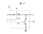
- FIG. 4 is an explanatory view showing an example of a circuit in the switching circuit 22 of FIG.
- FIG. 5 is an explanatory view showing another circuit example of the switching circuit 22 of FIG.
- step-down switching circuit each show an example of a step-down switching circuit.
- a direct current input voltage is time-divided by a switch and smoothed by a coil and a capacitor (not shown) to obtain a desired DC (direct current) output voltage.
- the switching circuit 22 shown in FIG. 4 is a synchronous step-down switching circuit, and has switches 41 and 43.
- the switches 41 and 43 are switched ON / OFF by control signals C1H and C1L, respectively.
- the control signals C1H and C1L are output from, for example, the transition management unit 25 of FIG. Ideally, the ON and OFF states of the switch 41 and the switch 43 are reversed.
- the switching circuit 22 shown in FIG. 5 is an example of an asynchronous step-down switching circuit, and has a switch 41 and a diode 42.
- the basic operation is the same as that of the synchronous switching circuit shown in FIG. 4 except that the switch connected to the ground which is the reference potential is replaced with the diode 42.
- the switch 41 is switched ON / OFF by the control signal C1.
- the control signal C1 is output from, for example, the transition management unit 25 of FIG.
- the configuration of the switching circuit 22 will be described on the premise that it is the asynchronous step-down switching circuit of FIG.
- the control signal to be added may be generated by inverting the original control signal in consideration of the dead time.
- FIG. 6 is a block diagram showing an example of the transition management unit 25 included in the power supply circuit 210 of FIG.
- transition management unit 25 for three power supply channels will be described for simplification.
- the transition management unit 25 includes level shift units 51-1 to 51-3, output error detection units 52-1 to 52-3, control signal generation units 53-1 to 53-3, and a delay unit. 54-1 to 54-3, a reference voltage generation unit 55, and a transition determination unit 56.
- the control signal generation units 53-1 to 53-3 are collectively referred to as the control signal generation unit 53.
- the delay units 54-1 to 54-3 are generally referred to as the delay unit 54.
- the level shift unit 51, the output error detection unit 52, the control signal generation unit 53, and the reference voltage generation unit 55 constitute an output voltage correction unit.
- the level shift unit 51 converts the output voltage Vout to the load so as to be comparable to the reference voltage Vref.
- the level shift unit 51 outputs the converted voltage to the output error detection unit 52.
- the reference voltage generation unit 55 generates a reference voltage Vref.
- the output error detection unit 52 outputs the difference between the voltage output from the level shift unit 51 and the reference voltage Vref generated by the reference voltage generation unit 55.
- the control signal generation unit 53 generates an intermediate control signal C ′ from the triangular wave input from the clock generation unit 26 and the difference output from the output error detection unit 52.
- the intermediate control signal C ' is a PWM signal.
- the intermediate control signals output from the control signal generation units 53-1, 53-2, and 53-3 are intermediate control signals C1 ', C2', and C3 ', respectively.
- the intermediate control signal C ′ may be a 1-bit signal of 1 (high) or 0 (low), and is a signal for turning on and off the switch, respectively.
- periods Tp1, Tp2, and Tp3 of the triangular wave input from the clock generation unit 26 to the control signal generation units 53-1, 53-2, and 53-3 are set to times T, 2T, and 4T, respectively.
- the switching frequency which is the reciprocal of these, increases the switching loss and lowers the power supply efficiency if it is high, but the response to load fluctuation is high, and the reverse is the case if it is low.
- the Tp3 4T power supply channel assumes an FPGA with relatively high current consumption, relatively low operating frequency, and low load fluctuation.
- the power supply channel of Tp2 2T assumes the GPU which is in between these.
- the required delay amount of each power supply channel is derived by performing arithmetic processing using each sampled signal, and a command signal is sent to the delay unit 54. Details of the transition determination by the transition determination unit 56 will be described later.
- FIG. 7 is a flowchart showing an example of the transition determination process performed by the transition management unit 25 of FIG.
- the transition determination process is a process of reducing the current ripple of the input current IinS of the power supply circuit 210.
- the transition management unit 25 detects the instantaneous value of the conduction noise is shown. Further, as in FIG. 5, for the sake of simplicity, the transition management unit 25 is described as being for three power supply channels.
- the transition management unit 25 updates the internal counter value t of the transition management unit 25 to 0, and reads control information of the set operation mode from the management database 27 (step S101). Details of the management database 27 will be described later.
- the process waits until the timing signal output from the clock generation unit 26 is received (step S102). Then, when the timing signal is received, the counter value t is incremented, and the intermediate control signals C1 ', C2' and C3 'of the respective power supply channels are sampled according to the timing signal C1' (t), C2 '(t), C3 '(t) is acquired (step S103).
- ImN is a current coefficient which is one of the control information read from the management database 27.
- step S106 is performed such that
- ⁇ IinN (t) of the power supply channel with high priority is subtracted from ⁇ IinS (t) according to the priority information which is one of the control information read from the management database 27.
- step S106 the subtraction result is replaced with ⁇ IinS (t), and the same subtraction is repeated until the following equation is established (step S106).
- subtraction is performed according to the priority, it may be subtracted from a power supply channel in which
- step S107 it is determined whether or not the above equation 6 is satisfied (step S107), and if it is not satisfied, a warning is output to the host system such as ECU that manages the power (step S110). This processing ends.
- a command signal is sent to the delay unit 54 so as to delay the power supply channel thus subtracted by the delay amount TdN which is one of the control information read from the management database 27 (step S108).
- step S109 it is checked whether or not there is an operation mode switching command from the host system. If there is a switching instruction, the present process is ended. If not, the process returns to step S102 to continue the present process.
- FIG. 8 is an explanatory view showing an example of the data configuration in the management database 27 of the power supply circuit 210 of FIG.
- the operation mode 72 is associated with control information 73-1 to control information 73-6 which are parameters of transition determination processing of the corresponding mode.
- control information 73-1 to control information 73-6 are collectively referred to, they are simply described as the control information 73.
- the management database 27 is referred to by the transition management unit 25.
- the operation mode 72 shows an application example in automatic driving, for example, mode A which is an urban area traveling mode, mode B which is an expressway traveling mode, mode C which is a parking mode, and abnormality detection of the ECU.
- the mode is mode D.
- control information 73 corresponding to the operation mode 72 detection information of conduction noise is stored in the control information 73-1.
- control information 73-1 performs instantaneous value detection and average value detection in normal operation, that is, modes A to C, but performs only instantaneous value detection in mode ECU abnormality, ie, emergency in mode D. Setting.
- the control information 73-2 stores, for example, information of a time span Ts at which the intermediate control information C 'is sampled.
- the time span may be reduced according to the operation mode, or the time span may be set larger to perform calculation processing with lower delay.
- a command signal may be output and controlled so as to generate a clock according to the clock generation unit 26.
- the clock generation unit 26 may be made to generate a short cycle timing signal beforehand, and the transition determination unit 56 may be appropriately thinned and used.
- the current variation threshold may be set separately for ⁇ Ithpk and ⁇ Ithav in instantaneous value detection and average value detection. These numerical values are set, for example, with reference to a standard value of conducted noise.
- the control information 73-4 stores information of current coefficients Im1 to ImN for calculating the input current of each switching circuit 22.
- the current coefficients Im1 to ImN are set based on, for example, the maximum current flowing to the load connected to each switching circuit 22 which is derived in advance by simulation or measurement.
- the control information 73-5 stores information on delay amounts Td1 to TdN corresponding to each power supply channel.
- the transition management unit 25 determines the amount of delay to be delayed by the delay unit 54 according to this information.
- the control information 73-6 stores information on the priority of transition management of each power supply channel. The higher the priority here, the higher the priority to be delayed. In other words, the power supply channel for supplying power to core logic and the like responsible for highly reliable operation is set to have a low priority.
- the transition determination process may be changed according to the operation mode.
- the management database 27 may additionally change the operation mode and control information of the automatic driving from the server on the cloud or the like via the wireless network by OTA.
- the update data is transferred to the wireless communication unit 105 of the on-vehicle system 10 of FIG.
- the wireless communication unit 105 transfers the received update data to the transition management unit 25 of the autonomous traveling control ECU 201. This completes the process of adding and changing the operation mode and control information of the automatic driving.
- transition control information used in the added operation mode is additionally introduced into the power supply circuit 210 without affecting the operation mode in use. Can.
- the current fluctuation threshold value ⁇ Ith of the control information 73-3 may be set according to the peripheral environment of the vehicle or the arithmetic processing of the SoC 211 of FIG. Specifically, when traveling in an urban area is performed in mode A, which is an urban area traveling mode, the current fluctuation threshold ⁇ Ith is set according to the crowded state of the road, for example, whether it is traffic jam or not traffic jam. Set The same applies to the mode B which is the expressway travel mode. Thereby, the control signal C can be generated more precisely, and the conduction noise of the input current can be accurately reduced. ⁇ effect>
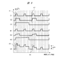
- FIG. 9 is a schematic view showing an example of each signal waveform in the power supply circuit examined by the present inventor.
- FIG. 9 shows an example of the transition management unit having no delay control function by the transition determination process shown in FIG. 7 etc., and from the top to the bottom, the control signals C1 ⁇ output from the transition management unit Signal timings of waveforms of C3, input currents Iin1 to Iin3 to the switching circuit, and input current IinS of the power supply circuit are shown.
- the horizontal axis is the timing signal described in FIG.
- the periods Tp1, Tp2 and Tp3 of the control signals are T, 2T and 4T, respectively, and the period Ts of the timing signal from the clock generation unit 26 is T / 10. .
- the input current to the switching circuit behaves like Iin1 to Iin3 according to each control signal C1 to C3, and the input current waveform to the power supply circuit, which is the sum thereof, becomes like IinS.
- IinS is a conducted noise standard at the point A3. It has ⁇ IinS (3) larger than the current fluctuation threshold ⁇ Ith set based on the value.
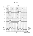
- FIG. 10 is a schematic view showing an example of each signal waveform in the power supply circuit 210 of the transition management unit 25 shown in FIG.
- control signals of control signals C2 and C3 are compared with those in FIG. 9 so that .DELTA.IinS (3) does not exceed current variation threshold value .DELTA.Ith by the transition determination processing described in FIGS. They are delayed by 3Ts and 5Ts respectively.
- ⁇ IinS (3) at point A3 in FIG. 9 is greatly reduced and falls below ⁇ Ith, as shown at point B3 in FIG.
- ⁇ IinS at point B4 in FIG. 10 is larger than that at point B3, but smaller than ⁇ Ith.
- the switching frequency of the third switching circuit is selected to be an integral multiple of the switching frequency of the two switching circuits. There is almost no need to perform delay control of Further, although the switching frequencies of the three switching circuits are all different here, the effect similar to that of the present embodiment can be obtained by changing only one.
- the control device for automatic operation having a large number of power supply channels is also input. Conducted noise of current can be effectively reduced.
- the transition management unit 25 dynamically controls the delay of the control signal to reduce the conducted noise.
- a technique for performing static control will be described.
- FIG. 11 is an explanatory drawing showing an example of the configuration of the transition management unit 25 according to the second embodiment.
- transition management unit 25 largely different from the first embodiment will be mainly described with reference to FIG.
- the transition management unit 25 is described as performing transition determination processing for three power supply channels for simplification.
- the transition management unit 25 includes level shift units 51-1 to 51-3, output error detection units 52-1 to 52-3, control signal generation units 53-1 to 53-3, and a delay unit. 54-1 to 54-3 and a reference voltage generation unit 55.
- the difference between the transition management unit 25 of FIG. 11 and the transition management unit 25 of FIG. 6 of the first embodiment is that the transition determination unit 56 is not provided.
- level shift units 51-1 to 51-3 are collectively referred to, they are simply described as the level shift unit 51, and when the output error detection units 52-1 to 52-3 are collectively referred to, the output error detection is simply performed. It describes as the part 52.
- control signal generation units 53-1 to 53-3 When the control signal generation units 53-1 to 53-3 are collectively referred to, they are simply referred to as the control signal generation unit 53.
- delay units 54-1 to 54-3 When the delay units 54-1 to 54-3 are collectively referred to, the delay unit 54 is simply referred to. And write.
- the level shift unit 51 converts the output voltage Vout to the load so as to be comparable to the reference voltage Vref, and outputs the voltage to the output error detection unit 52 at the next stage.
- the output error detection unit 52 outputs the difference between the input voltage from the level shift unit 51 and the reference voltage Vref.
- the reference voltage generation unit 55 generates a reference voltage Vref.
- the control signal generation unit 53 generates intermediate control signals C1 ', C2' and C3 'which are PWM signals from the triangular wave inputted from the clock generation unit 26 and the difference outputted from the output error detection unit 52.
- periods Tp1, Tp2, and Tp3 of the triangular wave input from the clock generation unit 26 to the control signal generation units 53-1, 53-2, and 53-3 are T, 2T, and 4T, respectively.
- the delay unit 54 delays the intermediate control signals C1 ', C2' and C3 'by preset delay amounts Td1, Td2 and Td3 and outputs control signals C1, C2 and C3.
- the delay amount of the delay unit 54 is preset.
- the delay amount is set by deriving or measuring in advance whether or not the conducted noise falls within the allowable value if the delay amount of each switching circuit is set. Do.
- the power supply circuit 210 has a configuration obtained by removing the management database 27 from the configuration shown in FIG. 3 of the first embodiment.
- the input current Iin of the switching circuit 22 is estimated from the intermediate control signal C ′.
- the input current Iin is directly measured to accurately conduct the conduction noise.
- the power supply circuit and transition management unit different from the first embodiment will be mainly described below with reference to FIGS. 12 and 13.
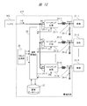
- FIG. 12 is a block diagram showing an example of a configuration of the power supply circuit 210 according to the third embodiment.
- the power supply circuit 210 of FIG. 12 differs from the power supply circuit 210 of FIG. 3 in that current sensors 28-1 to 28-N which are current measurement units are newly provided.
- current sensors 28-1 to 28-N are collectively referred to, they are simply referred to as the current sensor 28.
- the current sensors 28-1 to 28-N are provided at the input portions of the switching circuits 22-1 to 22-N, respectively, and measure the input currents Iin1 to IinN.
- the measurement results measured by the current sensors 28 are sent to the transition management unit 25 and used in transition determination processing described later.
- the current sensor 28 may use, for example, a current detection circuit using a current transformer, a Hall element, a GMR (Giant Magneto Resistive effect) element, or the like.
- a current sensor that measures the input current IinS of the power supply circuit 210 may be added.
- FIG. 13 is an explanatory diagram showing an example of a configuration of the transition management unit 25 included in the power supply circuit 210 of FIG.
- transition management unit 25 performs transition determination processing for three power supply channels.
- the transition management unit 25 includes level shift units 51-1 to 51-3, output error detection units 52-1 to 52-3, control signal generation units 53-1 to 53-3, and delay units 54-1 to 54-3. , A reference voltage generation unit 55, and a transition determination unit 56.
- the level shift unit 51 converts the output voltage Vout to the load so as to be comparable to the reference voltage Vref generated by the reference voltage generation unit 55, and outputs the converted voltage to the output error detection unit 52 of the next stage.
- the output error detection unit 52 outputs the difference between the voltage output from the level shift unit 51 and the reference voltage Vref.
- the control signal generation unit 53 generates intermediate control signals C1 ', C2' and C3 'which are PWM signals from the triangular wave inputted from the clock generation unit 26 and the difference outputted from the output error detection unit 52.
- periods Tp1, Tp2, and Tp3 of the triangular wave input from the clock generation unit 26 to the control signal generation units 53-1, 53-2, and 53-3 are T, 2T, and 4T, respectively.
- the input current of the switching circuit 22 is measured by the current sensor 28, and the delay amount of the control signal is set in advance based on the total value of the change amount, thereby an electronic control device having a large number of power supply channels, Also in the autonomous traveling control ECU 201, the conduction noise of the input current can be controlled with higher accuracy.
- the present invention is not limited to the above-mentioned embodiment, and can be variously changed in the range which does not deviate from the gist. Needless to say.
- the present invention is not limited to the above-described embodiment, but includes various modifications.
- the above-described embodiments are described in detail to explain the present invention in an easy-to-understand manner, and are not necessarily limited to those having all the described configurations.
- part of the configuration of one embodiment can be replaced with the configuration of another embodiment, and the configuration of another embodiment can be added to the configuration of one embodiment. .
- each of the configurations, functions, processing units, processing means, etc. described above may be realized by hardware, for example, by designing part or all of them with an integrated circuit. Further, each configuration, function, etc. described above may be realized by software by the processor interpreting and executing a program that realizes each function. Information such as a program, a table, and a file for realizing each function can be placed in a memory, a hard disk, a recording device such as a solid state drive (SSD), or a recording medium such as an IC card, an SD card, or a DVD.
- SSD solid state drive
- control lines and information lines indicate what is considered to be necessary for the description, and not all control lines and information lines in the product are necessarily shown. In practice, almost all configurations may be considered to be mutually connected.
Landscapes
- Engineering & Computer Science (AREA)
- Power Engineering (AREA)
- Mechanical Engineering (AREA)
- Automation & Control Theory (AREA)
- Human Computer Interaction (AREA)
- Transportation (AREA)
- Dc-Dc Converters (AREA)
Abstract
L'invention réduit le bruit conduit d'un courant d'entrée dans un dispositif d'alimentation électrique ayant une pluralité de canaux à faible coût. Dans un circuit d'alimentation électrique (210) assujetti à une ECU de commande à fonctionnement autonome, des circuits de commutation (22) génèrent respectivement, sur la base de signaux de commande C, l'énergie électrique alimentant une pluralité de circuits logiques. Une unité de gestion de transition (25) commande les circuits de commutation (22). Une unité de génération d'horloge (26) génère une pluralité de signaux d'horloge. L'unité de gestion de transition (25) comprend une unité de génération de signaux de commande et une pluralité d'unités de retard. L'unité de génération de signaux de commande génère des signaux de commande intermédiaires à partir des signaux d'horloge générés par l'unité de génération d'horloge (26). Les unités de retard retardent les signaux de commande intermédiaires sur la base de signaux de commande, et émettent les signaux de commande intermédiaires retardés en tant que signaux de commande C. Les signaux d'horloge générés par l'unité de génération d'horloge comprennent au moins un signal d'horloge d fréquence différente.
Priority Applications (2)
| Application Number | Priority Date | Filing Date | Title |
|---|---|---|---|
| US16/760,136 US10938305B2 (en) | 2017-11-13 | 2018-09-13 | Electronic control device, in-vehicle system, and power supply device |
| DE112018004580.3T DE112018004580T5 (de) | 2017-11-13 | 2018-09-13 | Elektronisches steuergerät, bordsystem und stromversorgungsgerät |
Applications Claiming Priority (2)
| Application Number | Priority Date | Filing Date | Title |
|---|---|---|---|
| JP2017218505A JP7004547B2 (ja) | 2017-11-13 | 2017-11-13 | 電子制御装置、車載システム、および電源装置 |
| JP2017-218505 | 2017-11-13 |
Publications (1)
| Publication Number | Publication Date |
|---|---|
| WO2019092982A1 true WO2019092982A1 (fr) | 2019-05-16 |
Family
ID=66437732
Family Applications (1)
| Application Number | Title | Priority Date | Filing Date |
|---|---|---|---|
| PCT/JP2018/033927 Ceased WO2019092982A1 (fr) | 2017-11-13 | 2018-09-13 | Dispositif de commande électronique, système embarqué et dispositif d'alimentation électrique |
Country Status (4)
| Country | Link |
|---|---|
| US (1) | US10938305B2 (fr) |
| JP (1) | JP7004547B2 (fr) |
| DE (1) | DE112018004580T5 (fr) |
| WO (1) | WO2019092982A1 (fr) |
Families Citing this family (5)
| Publication number | Priority date | Publication date | Assignee | Title |
|---|---|---|---|---|
| US11435438B2 (en) * | 2019-12-30 | 2022-09-06 | Woven Planet North America, Inc. | Dynamic sparse radar array for scenarios |
| CN112653116B (zh) * | 2020-12-18 | 2022-11-01 | 中国科学院国家空间科学中心 | 一种面向低母线电压的低emi星载二次电源系统 |
| US12273075B2 (en) * | 2021-07-01 | 2025-04-08 | Epirus, Inc. | Systems and methods for power distribution for amplifier arrays |
| CN113783651B (zh) * | 2021-09-10 | 2024-02-06 | 阿波罗智能技术(北京)有限公司 | 平行驾驶的远程控制方法、装置、云端、车端及平行驾驶系统 |
| CN117922461A (zh) * | 2022-10-14 | 2024-04-26 | 神基科技股份有限公司 | 车辆电源供应回路监控系统及车辆电源供应回路监控方法 |
Citations (5)
| Publication number | Priority date | Publication date | Assignee | Title |
|---|---|---|---|---|
| JPS63245254A (ja) * | 1987-03-30 | 1988-10-12 | Toshiba Corp | スイツチングレギユレ−タ |
| JP2003259634A (ja) * | 2002-03-01 | 2003-09-12 | Auto Network Gijutsu Kenkyusho:Kk | 負荷駆動回路及び負荷駆動方法 |
| WO2015136746A1 (fr) * | 2014-03-12 | 2015-09-17 | 日本電気株式会社 | Dispositif d'alimentation électrique et procédé de fonctionnement de dispositif d'alimentation électrique |
| WO2016080452A1 (fr) * | 2014-11-19 | 2016-05-26 | エイディシーテクノロジー株式会社 | Dispositif de commande de conduite autonome |
| JP2017153218A (ja) * | 2016-02-23 | 2017-08-31 | 富士通株式会社 | 電源装置 |
Family Cites Families (4)
| Publication number | Priority date | Publication date | Assignee | Title |
|---|---|---|---|---|
| JP5897642B2 (ja) * | 2014-05-30 | 2016-03-30 | ファナック株式会社 | Dc/dcコンバータ |
| JP5911030B2 (ja) | 2014-09-03 | 2016-04-27 | 三菱電機株式会社 | デジタル制御電源装置 |
| CN108141130A (zh) * | 2015-09-15 | 2018-06-08 | 日本电气株式会社 | 切换电源设备、切换电源的驱动方法和切换电源的驱动程序 |
| CN106533136B (zh) * | 2016-12-19 | 2019-03-22 | 成都芯源系统有限公司 | 多通道开关电源及其控制器和控制方法 |
-
2017
- 2017-11-13 JP JP2017218505A patent/JP7004547B2/ja active Active
-
2018
- 2018-09-13 WO PCT/JP2018/033927 patent/WO2019092982A1/fr not_active Ceased
- 2018-09-13 DE DE112018004580.3T patent/DE112018004580T5/de active Granted
- 2018-09-13 US US16/760,136 patent/US10938305B2/en active Active
Patent Citations (5)
| Publication number | Priority date | Publication date | Assignee | Title |
|---|---|---|---|---|
| JPS63245254A (ja) * | 1987-03-30 | 1988-10-12 | Toshiba Corp | スイツチングレギユレ−タ |
| JP2003259634A (ja) * | 2002-03-01 | 2003-09-12 | Auto Network Gijutsu Kenkyusho:Kk | 負荷駆動回路及び負荷駆動方法 |
| WO2015136746A1 (fr) * | 2014-03-12 | 2015-09-17 | 日本電気株式会社 | Dispositif d'alimentation électrique et procédé de fonctionnement de dispositif d'alimentation électrique |
| WO2016080452A1 (fr) * | 2014-11-19 | 2016-05-26 | エイディシーテクノロジー株式会社 | Dispositif de commande de conduite autonome |
| JP2017153218A (ja) * | 2016-02-23 | 2017-08-31 | 富士通株式会社 | 電源装置 |
Also Published As
| Publication number | Publication date |
|---|---|
| US20200254947A1 (en) | 2020-08-13 |
| US10938305B2 (en) | 2021-03-02 |
| JP7004547B2 (ja) | 2022-01-21 |
| JP2019092265A (ja) | 2019-06-13 |
| DE112018004580T5 (de) | 2020-11-12 |
Similar Documents
| Publication | Publication Date | Title |
|---|---|---|
| US10938305B2 (en) | Electronic control device, in-vehicle system, and power supply device | |
| CN106716173B (zh) | 用于运行机动车中多个雷达传感器的方法和机动车 | |
| KR101423871B1 (ko) | 시험장치 | |
| US9444248B2 (en) | Control circuit for limiting a load current, charging circuit and motor vehicle | |
| US8698469B1 (en) | System and method for predicting output voltage ripple and controlling a switched-mode power supply | |
| CN102684475B (zh) | Dc/dc降压转换器中用于负载电流的前馈控制的系统和方法 | |
| US20170075404A1 (en) | Semiconductor device | |
| US8228014B2 (en) | Multi-phase DC/DC boost converter | |
| US9467058B2 (en) | Method and apparatus for controlling output voltage of DC-DC converter | |
| US10132843B2 (en) | Detector and a voltage converter | |
| US20180191185A1 (en) | Battery Switching System | |
| US9829944B2 (en) | Multiphase voltage regulator using coupled inductors | |
| US20120113701A1 (en) | Inverter current measurement using a shunt resistor | |
| US9705410B2 (en) | Power conversion apparatus | |
| US9667135B2 (en) | Multiphase DC voltage converter and method for controlling a multiphase DC voltage converter | |
| CN113614550A (zh) | 用于分析耗电器中的电流的设备和具有这种设备的耗电器 | |
| US9401641B2 (en) | Systems and methods for self-calibration of a voltage regulator | |
| US20200348740A1 (en) | Smart controller with phantom inductor current sensing for switched mode power supplies | |
| US20200055467A1 (en) | Electronic Control Device, In-Vehicle System, and Power Supply Device | |
| CN109213297B (zh) | 半导体装置以及半导体装置的控制方法 | |
| CN108736792A (zh) | 矩阵变换器以及交流电动机的常数确定方法 | |
| US12601769B2 (en) | Input isolated voltage monitor | |
| CN106291424B (zh) | 用于测定所测量的电流实际值与电流额定值的偏差的方法 | |
| JP5456422B2 (ja) | パワーエレクトロニクスシステムの状態の評価方法 | |
| US20240372479A1 (en) | Dc-to-dc converters |
Legal Events
| Date | Code | Title | Description |
|---|---|---|---|
| 121 | Ep: the epo has been informed by wipo that ep was designated in this application |
Ref document number: 18875471 Country of ref document: EP Kind code of ref document: A1 |
|
| 122 | Ep: pct application non-entry in european phase |
Ref document number: 18875471 Country of ref document: EP Kind code of ref document: A1 |