WO2019146399A1 - Dispositif de test de condensateur, dispositif de conversion d'énergie électrique et procédé de test de condensateur - Google Patents
Dispositif de test de condensateur, dispositif de conversion d'énergie électrique et procédé de test de condensateur Download PDFInfo
- Publication number
- WO2019146399A1 WO2019146399A1 PCT/JP2019/000292 JP2019000292W WO2019146399A1 WO 2019146399 A1 WO2019146399 A1 WO 2019146399A1 JP 2019000292 W JP2019000292 W JP 2019000292W WO 2019146399 A1 WO2019146399 A1 WO 2019146399A1
- Authority
- WO
- WIPO (PCT)
- Prior art keywords
- capacitor
- test
- ripple current
- circuit
- capacitors
- Prior art date
- Legal status (The legal status is an assumption and is not a legal conclusion. Google has not performed a legal analysis and makes no representation as to the accuracy of the status listed.)
- Ceased
Links
Images








Classifications
-
- G—PHYSICS
- G01—MEASURING; TESTING
- G01R—MEASURING ELECTRIC VARIABLES; MEASURING MAGNETIC VARIABLES
- G01R27/00—Arrangements for measuring resistance, reactance, impedance, or electric characteristics derived therefrom
- G01R27/02—Measuring real or complex resistance, reactance, impedance, or other two-pole characteristics derived therefrom, e.g. time constant
-
- G—PHYSICS
- G01—MEASURING; TESTING
- G01R—MEASURING ELECTRIC VARIABLES; MEASURING MAGNETIC VARIABLES
- G01R27/00—Arrangements for measuring resistance, reactance, impedance, or electric characteristics derived therefrom
- G01R27/02—Measuring real or complex resistance, reactance, impedance, or other two-pole characteristics derived therefrom, e.g. time constant
- G01R27/26—Measuring inductance or capacitance; Measuring quality factor, e.g. by using the resonance method; Measuring loss factor; Measuring dielectric constants ; Measuring impedance or related variables
-
- G—PHYSICS
- G01—MEASURING; TESTING
- G01R—MEASURING ELECTRIC VARIABLES; MEASURING MAGNETIC VARIABLES
- G01R31/00—Arrangements for testing electric properties; Arrangements for locating electric faults; Arrangements for electrical testing characterised by what is being tested not provided for elsewhere
-
- H—ELECTRICITY
- H01—ELECTRIC ELEMENTS
- H01G—CAPACITORS; CAPACITORS, RECTIFIERS, DETECTORS, SWITCHING DEVICES, LIGHT-SENSITIVE OR TEMPERATURE-SENSITIVE DEVICES OF THE ELECTROLYTIC TYPE
- H01G13/00—Apparatus specially adapted for manufacturing capacitors; Processes specially adapted for manufacturing capacitors not provided for in groups H01G4/00 - H01G11/00
Definitions
- the present invention relates to a capacitor test apparatus, a power converter and a capacitor test method.
- Power converters such as inverters and converters are used within a defined maximum rated power range even if the mounted capacitors deteriorate.
- the capacitor used for this application is required to ensure the life and quality when operated for a long time at the maximum rated power, and it is necessary to perform a stress application test in which the power applied to the capacitor is constant.
- an object of the present invention is to provide a capacitor test apparatus, a power converter and a capacitor test method capable of performing reliable quality test.
- the present invention is a capacitor test apparatus for testing the quality of a test target capacitor, which includes a ripple current generation circuit that applies a ripple current to the test target capacitor, and a ripple current based on a change in the electrical characteristics of the test target capacitor. And a controller for adjusting the ripple current generated by the ripple current generation circuit when the test is continued.
- the present invention is a capacitor test method for testing the quality of a test target capacitor, and adjusting the ripple current based on the step of applying a ripple current to the test target capacitor and the change in the electrical characteristics of the test target capacitor. , Adjusting the ripple current when continuing the test.
- the power applied to the capacitor under test can be kept constant by adjusting the ripple current flowing through the capacitor under test based on the change in the electrical characteristics of the capacitor under test.
- the load environment of the capacitor in the mounted device can be accurately reproduced, and a highly reliable quality test can be performed.
- FIG. 2 is a diagram showing a capacitor test apparatus 150 and capacitors under test 12a to 12c according to a first embodiment.
- FIG. 2 is a diagram showing a configuration of a power conversion device 151 of a first embodiment.
- 7 is a flowchart showing a control procedure of a ripple current application test of the first embodiment. It is a flowchart showing the procedure which measures the equivalent series resistance of a test object capacitor. It is a figure which shows the voltage waveform between XY at the time of equivalent series resistance measurement. It is a flowchart showing the procedure which measures the electrostatic capacitance of a test object capacitor.
- FIG. 1 is a diagram showing a capacitor test apparatus 150 and capacitors under test 12a to 12c according to a first embodiment.
- FIG. 2 is a diagram showing a configuration of a power conversion device 151 of a first embodiment.
- 7 is a flowchart showing a control procedure of a ripple current application test of the first embodiment. It is a flowchart showing the procedure which measures
- FIG. 7 is a diagram showing a voltage waveform between XY at the time of capacitance measurement and a waveform of a combined current I of a capacitor to be tested. It is a timing chart of the current and voltage which ripple current generation circuit 100 generates. It is a flowchart showing the control procedure of the ripple current application test of the modification of Embodiment 1.
- FIG. FIG. 16 is a diagram showing a capacitor test apparatus 150 according to a second embodiment.
- FIG. 16 is a diagram showing a capacitor test apparatus 150 according to a third embodiment.
- FIG. 16 is a diagram showing a capacitor test apparatus 150 according to a fourth embodiment.
- FIG. 18 is a diagram showing a capacitor test apparatus 150 according to a fifth embodiment.
- FIG. 18 is a diagram showing a capacitor test apparatus 150 according to a sixth embodiment. It is a figure showing the power converter device of Embodiment 7.
- FIG. FIG. 35 is a diagram showing a power conversion apparatus 1000 according to an eighth embodiment.
- FIG. 21 is a diagram illustrating a power conversion system according to a ninth embodiment. It is a flowchart showing the procedure which measures the parasitic inductance of the direct current transmission cable of Embodiment 9. It is a flowchart showing the control procedure of the parasitic inductance measurement of the wiring of Embodiment 9.
- FIG. 40 is a diagram showing a voltage waveform between XY at the time of measuring a parasitic inductance of the wiring of the ninth embodiment and a waveform of a combined current I of a capacitor to be tested.
- FIG. 24 is a diagram showing a voltage waveform between XY and a waveform of a combined current I of a test object capacitor at the time of measuring a parasitic inductance of a wire immediately after the start of charging of the test object capacitors 12a to 12c of the ninth embodiment.
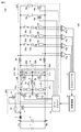
- FIG. 1 is a diagram showing capacitor test apparatus 150 and capacitors 12 a to 12 c to be tested according to the first embodiment.
- the power conversion device for driving the motor by the inverter may include the capacitor test device 150 of FIG. 1 in order to test the built-in capacitors 12a to 12c.
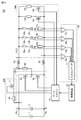
- FIG. 2 shows a configuration of power conversion device 151 of the first embodiment.
- the power converter 151 includes a capacitor test device 150 and capacitors 12a to 12c.
- the power conversion device 151 may include the capacitor test device 150 and the capacitors 12a to 12c.
- Capacitor testing apparatus 150 tests the quality of capacitors 12a to 12c as capacitors to be tested.
- Capacitor test apparatus 150 includes DC power supply 1, capacitor 2, current backflow preventing diode 3, switching element 4, ripple current generation circuit 100, charging circuit 200, coils 8a and 8b, and discharging circuit 300.
- the current detection resistors 13a to 13c, the measurement circuit 60, the gate driver 19, and the control device 18 are provided.
- test target capacitors 12a to 12c may be collectively referred to as the test target capacitor 12, and the current detection resistors 13a to 13c may be collectively referred to as the current detection resistor 13.
- the capacitors 12a to 12c to be tested are aluminum electrolytic capacitors, solid capacitors, hybrid capacitors, oil capacitors, film capacitors, ceramic capacitors, electric double layer capacitors, lithium ion capacitors, etc., but the type is not particularly limited. .
- Test target capacitor 12a and current detection resistor 13a are connected in series between node X on positive electrode line PL and node Y on negative electrode line NL.
- Test target capacitor 12 b and current detection resistor 13 b are connected in series between node X on positive electrode line PL and node Y on negative electrode line NL.
- Test target capacitor 12 c and current detection resistor 13 c are connected in series between node X on positive electrode line PL and node Y on negative electrode line NL.
- the charging circuit 200 charges the test target capacitors 12a to 12c in order to measure the electrical characteristics of the test target capacitors 12a to 12c.
- the charging circuit 200 is used to measure the capacitance and the like of the test target capacitors 12a to 12c.
- Charging circuit 200 includes switching element 11 and charging resistor 10 connected in series between node C on positive electrode line PL and node D on positive electrode line PL.
- Switching element 11 is formed of, for example, a MOSFET (Metal-Oxide-Semiconductor Field-Effect Transistor).
- MOSFET Metal-Oxide-Semiconductor Field-Effect Transistor
- the discharge circuit 300 discharges the test target capacitors 12a to 12c in order to measure the electrical characteristics of the test target capacitors 12a to 12c.
- the discharge circuit 300 is used to measure the capacitance and the like of the test target capacitors 12a to 12c.
- Discharge circuit 300 includes switching element 14a and discharge resistor 15a connected in series between node X on positive electrode line PL and node Y on negative electrode line NL, and on node X on positive electrode line PL and negative electrode line NL.
- the switching element 14 b and the discharge resistor 15 b are connected in series with the node Y.
- Switching elements 14a and 14b are formed of, for example, MOSFETs.
- the switching elements 14 a and 14 b are driven by the gate driver 19.
- the discharge resistor 15a is used to perform a large current discharge of the test object capacitor 12 when measuring the equivalent series resistance.
- the discharge resistor 15b is used to perform a small current discharge of the test target capacitor at the time of capacitance measurement.
- the switching elements 14 a and 14 b may be collectively referred to as the switching element 14.
- the discharge resistors 15a and 15b may be collectively referred to as a discharge resistor 15.
- DC power supply 1 is provided between node A on positive electrode line PL and node B on negative electrode line NL.
- the DC power supply 1 sets the charging voltage of the test target capacitor 12.
- Capacitor 2 is connected in parallel to DC power supply 1. Capacitor 2 suppresses the inrush current of DC power supply 1.
- the current backflow preventing diode 3 is provided between the node A on the positive electrode line PL and the node C on the positive electrode line PL.
- the current backflow preventing diode 3 is provided to prevent a regenerative current from flowing from the regenerative coil 6 to the DC power supply 1.
- Switching element 4 is provided between node C on positive electrode line PL and node D on positive electrode line PL.
- the switching element 4 connects and disconnects the ripple current generation circuit 100 and the DC power supply 1.
- Switching element 4 is formed of, for example, a MOSFET.
- the switching element 4 is driven by a gate driver 19.
- the ripple current generation circuit 100 applies a ripple current to the test target capacitors 12a to 12c.
- the ripple current generation circuit 100 includes a coil 6 for regeneration, switching elements 5a and 5b, diodes 7a and 7b, and a surge absorption capacitor 9.
- Switching element 5a is provided between node D on positive electrode line PL and node E.
- Diode 7 b is provided between node E and node B on negative line NL.
- the diode 7a is provided between the node D on the positive electrode line PL and the node F.
- Switching element 5b is provided between node F and node B on negative line NL.
- the diodes 7a and 7b During regeneration, the diodes 7a and 7b generate a regenerative current due to the electromotive force of the regenerative coil 6.
- the coil for regeneration 6 may be substituted by a load or a winding or coil of a motor connected as an electromotive force source.
- Diodes 7a and 7b are formed of, for example, high-speed recovery diodes. It is a diode that allows a regenerative current to flow by the electromotive force of the regenerative coil 6 during regeneration.
- Regeneration coil 6 is provided between node E and node F.
- the regenerative coil 6 is provided to exchange electrical energy with the capacitors 12a to 12c to be tested.
- the regenerative coil 6 can store the discharge current of the test target capacitor 12.
- the switching elements 5a and 5b adjust the timing and current amount of exchange of electrical energy between the capacitors 12a to 12c to be tested and the coil 6 for regeneration.
- Switching elements 5a and 5b are formed of, for example, a MOSFET.
- the switching elements 5 a and 5 b are driven by the gate driver 19.
- the switching elements 5a and 5b apply a regenerative current with an electromotive force by the regenerative coil 6 at the time of regeneration.
- the surge absorption capacitor 9 is provided between the node D on the positive electrode line PL and the node B on the negative electrode line NL.
- the surge absorption capacitor 9 eliminates switching surges.
- Coil 8a is provided between node D and node X on positive electrode line PL.
- Coil 8b is provided between node B and node Y on negative electrode line NL.
- the coils 8a and 8b suppress harmonics of the ripple current.
- the measurement circuit 60 measures the electrical characteristics of the test target capacitors 12a to 12c.
- the measurement circuit 60 includes input amplifiers 16 a to 16 d and an A / D converter 17.
- the input amplifier 16a measures the voltage of the node X on the positive electrode line PL and the node Y on the negative electrode line NL.
- the input amplifier 16b measures the voltage between the node G between the capacitor 12a to be tested and the current detection resistor 13a and the node Y on the negative electrode line NL, that is, the voltage across the current detection resistor 13a.
- the input amplifier 16c measures the voltage between the node H between the capacitor 12b to be tested and the current detection resistor 13b and the node Y on the negative electrode line NL, that is, the voltage across the current detection resistor 13b.
- the input amplifier 16c measures the voltage between the node I between the capacitor 12c to be tested and the current detection resistor 13c and the node Y on the negative electrode line NL, that is, the voltage across the current detection resistor 13c.
- the A / D converter 17 converts analog signals output from the input amplifiers 16a to 16d into digital values, and outputs the digital values to the control device 18.
- the controller 18 detects the voltage V between the node X and the node Y by the signal from the input amplifier 16a.
- the controller 18 detects the voltages Vg, Vh, and Vi at both ends of the current detection resistors 13a to 13c by the signals from the input amplifiers 16b to 16d.
- the gate driver 19 drives the switching elements 4, 5a, 5b, 11, 14a, 14b under the control of the control device 18.
- the controller 18 determines the degree of deterioration of the capacitors 12 a to 12 c under test according to the measured electrical characteristics, and adjusts the ripple current IR generated by the ripple current generation circuit 100 when the test is continued. For example, the controller 18 keeps the power applied to the capacitors under test 12a-12 constant by keeping the ripple current IR constant.
- the controller 18 determines the electrical characteristics of the capacitors 12 a to 12 c under test based on the voltages V, Vg, Vh and Vi. For example, the controller 18 sets at least one of the equivalent series resistance and capacitance, parasitic inductance, leakage current, dielectric loss tangent, dielectric loss, piezoelectric characteristics, and re-evoked voltage of the capacitors 12a to 12c to be tested as the electrical characteristics. Ask.
- the control device 18 adjusts the test conditions according to the judgment conditions and the sequence set in advance, and supplies the switching timing signal to the gate driver 19.
- the control device 18 intermittently interrupts the ripple current application test of the test target capacitors 12a to 12c while performing the ripple current application test of the test target capacitors 12a to 12c, and the combined capacitance C of the test target capacitors 12a to 12c. And the equivalent series resistance REa to REc.
- the controller 18 ends the test or adjusts the test conditions according to the measurement result, and restarts the ripple current application test.
- the controller 18 can also stop the test by detecting deterioration and abnormality of the capacitors 12a to 12c to be tested.
- the ripple current application test since the test of the test target capacitor 12 under test can be stopped, excessive deterioration and burnout of the test target capacitor 12 can be prevented, and a sample necessary for investigation of a deterioration process can be efficiently created.
- an excessive ripple current application test shortens the life of the device, so it is desirable to set a test termination condition according to the purpose.
- the number of capacitors under test 12 and current detection resistors 13 need not be three as shown in FIG. 1 and may be any number as long as it is one or more.
- the capacitor test device 150 When the capacitor test device 150 is incorporated in the power conversion device 151, the following may be used.
- the regenerative coil 6 can be substituted by a load of an impulseer, a motor used for an electromotive force source of a converter, a winding of a generator, or a coil of a generator.
- the current backflow preventing diode 3 may be omitted.
- the switching element 4 may be replaced by a current interrupting means other than a semiconductor element such as a relay machine, an electromagnetic switch, or a switch.
- the charging circuit 200 can be omitted.
- the discharge circuit 300 may be substituted by a load connected to the power conversion device 151 in some cases. When the power supply impedance of the DC power supply 1 is sufficiently low, the capacitor 2 and the surge absorption capacitor 9 may be able to be omitted.
- the current detection resistors 13a to 13c may be replaced by other current measurement means such as a current sensor or a current transformer.
- the ripple current generation circuit 100 is a half bridge circuit of a single phase inverter including two switching elements 5a and 5b.
- the ripple current generation circuit 100 is a full bridge circuit or an inverter of three or more phases or the like. It may be, and does not limit the type.
- the capacitor test device 150 is incorporated in the power conversion device 151, the power conversion device 151 itself may be able to be used as the ripple current generation circuit 100.
- the coils 8a and 8b may be parasitic inductances of wiring to the capacitor 12 under test.
- the current backflow preventing diode 3 is preferably a low loss diode such as a high speed recovery diode or a Schottky barrier diode, but the type is not limited as long as the rectifying characteristic is provided.
- the switching elements 4, 5a, 5b, 11, 14a, 14b preferably have low on-resistance and low loss, but MOSFETs or IGBTs (Insulated Gate Bipolar Transistors) or thyristors may be used. It is not limited.
- the DC power supply 1 may be selected from those that can be controlled by the control device 18.
- the A / D converter 17 may be built in the control device 18.
- the quality test of the capacitor to be tested will be described using the capacitor testing device of the first embodiment.
- the electrical characteristics of the test target capacitors 12a to 12 the equivalent series resistance and the combined capacitance of the test target capacitors 12a to 12c are used.
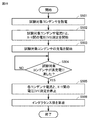
- FIG. 3 is a flowchart showing a control procedure of the ripple current application test of the first embodiment.
- step S101 a test start instruction is input to the control device 18.
- step S102 the control device 18 controls the discharge circuit 300 through the gate driver 19 to discharge the residual charge of the capacitors 12a to 12c under test.
- the residual charge may be generated by a re-electromotive voltage caused by the dielectric of the capacitors 12a to 12c to be tested.
- step S103 the control device 18 controls the charging circuit 200 through the gate driver 19 to charge the test target capacitors 12a to 12c for the connection confirmation and the initial characteristic evaluation of the test target capacitors 12a to 12c. Further, the control device 18 controls the discharge circuit 300 through the gate driver 19 to discharge the test target capacitors 12a to 12c. At the same time, the control device 18 causes the measuring circuit 60 to measure a voltage V between XY and a voltage Vg between YY and a voltage Vh between H and Y and a voltage Vi between I and Y.
- step S104 the control device 18 controls the discharge circuit 300 through the gate driver 19 to discharge the residual charge after measurement of the electrical characteristics of the capacitors 12a to 12c to be tested.
- step S105 the control device 18 obtains equivalent series resistances REa, REb, REc of the test target capacitors 12a to 12c based on the voltages V, Vg, Vh, and Vi measured in step S103. Details of this process will be described later.
- step S106 the control device 18 obtains the combined capacitance C of the test target capacitors 12a to 12c based on the voltages V, Vg, Vh, and Vi measured in step S103. Details of this process will be described later.
- step S107 the controller 18 obtains the degree of deterioration of the test target capacitors 12a to 12c based on at least one of the equivalent series resistance and capacitance of the test target capacitors 12a to 12c.
- the control device 18 can set the rate at which the combined capacitance of the test target capacitors 12a to 12 is reduced from the value of the predetermined product specification to the degree of deterioration of the test target capacitors 12a to 12c.
- the control device 18 can set the ratio of the average value or the maximum value of the equivalent series resistances of the test target capacitors 12a to 12 to a predetermined reference value to the degree of deterioration of the test target capacitors 12a to 12c.
- control device 18 determines whether the test object capacitors 12a to 12c are open or short-circuited based on whether voltage V between XY detected in step S105 satisfies a predetermined condition. Determine the abnormality.
- step S109 when the degree of deterioration of the test target capacitors 12a to 12c reaches the determination reference (S109: YES), the test is ended.
- the criterion of the degree of deterioration of the capacitors 12a to 12c to be tested can be set to 20%.
- step S110 when an abnormality such as the release or short circuit failure of the test target capacitors 12a to 12c is detected (S110: YES), the test is ended.
- step S110 If the deterioration degree of the test target capacitors 12a to 12c does not reach the determination reference and no abnormality is detected in the test target capacitors 12a to 12c (S109: NO, S110: NNO), the process proceeds to step S110.
- step S111 the control device 18 adjusts the ripple current IR generated by the ripple current generation circuit 100 according to at least one of the combined capacitance and the equivalent series resistance of the test target capacitors 12a to 12c.
- the duty ratio D of the control pulse applied to the switching elements 5a and 5b included in the ripple current generation circuit 100 is adjusted. If the duty ratio D is zero, the ripple current IR is zero. When the duty ratio D is set to the upper limit, the ripple current IR becomes maximum.
- Such adjustment makes it possible to improve the accuracy of the quality test by adjusting the ripple current IR applied in the test even if the capacitances of the capacitors 12a to 12c to be tested change.
- step S112 the control device 18 performs a ripple current application test for a fixed time.
- the ripple current application time be approximately several tens of seconds to several tens of minutes, but the ripple current application time should be set according to the type or characteristics of the capacitor 12 to be tested. Can. After interrupting the ripple current application test, the process returns to step S104.
- FIG. 4 is a flow chart showing a procedure for measuring the equivalent series resistance of the capacitor to be tested.
- step S201 the control device 18 turns on the switching element 11 in the charging circuit 200 through the gate driver 19 to fully charge the test target capacitors 12a to 12c.
- step S202 the control device 18 causes the measurement circuit 60 to measure the voltage V1 between XY.
- the voltage measurement point X is connected to the positive output of the ripple current generation circuit 100 and the positive terminals of the capacitors 12a to 12c to be tested.
- the negative terminals of the test target capacitors 12a to 12c are connected to the current detection resistors 13a to 13c, and the other terminals of the current detection resistors 13a to 13c are connected to the voltage measurement point Y and the negative output of the ripple current generation circuit 100. ing.
- step S203 the control device 18 turns on the switching element 14a in the discharge circuit 300 through the gate driver 19 to start discharging the test target capacitors 12a to 12c with a large current using the discharge resistor 15a.
- the control device 18 causes the measuring circuit 60 to measure the voltage V2 between XY. This voltage V2 is used in step S108 to determine an abnormality such as open or short circuit failure of the capacitors 12a to 12c to be tested.
- step S204 the control device 18 calculates equivalent series resistances REa, REb and REc of the test target capacitors 12a to 12c according to the equations (1) to (7).
- Ia Vg / Rsa (2)
- Ib Vh / Rsb (3)
- Ic Vi / Rsc (4)
- REa (Vd ⁇ Ia ⁇ Rsa) / Ia (5)
- REb (Vd ⁇ Ib ⁇ Rsb) / Ib (6)
- REc (Vd ⁇ Ic ⁇ Rsc) / Ic (7)
- Ia, Ib, Ic are currents flowing through the capacitors 12a, 12b, 12c to be tested.
- RSa, Rsb, and Rsc are resistance values of the current detection resistors 13a, 13b, and 13c.
- FIG. 5 is a diagram showing a voltage waveform between XY at the time of equivalent series resistance measurement. In FIG. 5, voltages V1, V2, Vd are shown.
- FIG. 6 is a flow chart showing a procedure of measuring the capacitance of the capacitor to be tested.
- step S301 the control device 18 turns on the switching element 11 in the charging circuit 200 through the gate driver 19 to fully charge the test target capacitors 12a to 12c.
- step S302 the control device 18 causes the measurement circuit 60 to measure the voltage V1 between XY.
- step S303 the control device 18 turns on the switching element 14b in the discharge circuit 300 through the gate driver 19 to start discharging the test target capacitors 12a to 12c with a small current using the discharge resistor 15b.
- step S304 the control device 18 weights the process by the sampling period ⁇ T.
- step S305 the control device 18 causes the measurement circuit 60 to measure the voltage V2 between XY.
- step S306 the control device 18 causes the measuring circuit 60 to measure the voltage Vg between G and Y, the voltage Vh between H and Y, and the voltage Vi between I and Y every sampling period ⁇ Ts.
- the controller 18 uses the voltages Vg, Vh and Vi to determine the currents Ia, Ib and Ic of the capacitors 12a, 12b and 12c to be tested according to the following equations.
- the currents obtained at the j-th sample are Ia (j), Ib (j) and Ic (j).
- the latest sampling is the n-th sampling.
- RSa, Rsb, and Rsc are resistance values of the current detection resistors 13a, 13b, and 13c.
- step S307 the control device 18 calculates the combined capacitance C of the test target capacitors 12a to 12c according to the following equation.
- Vs (Ia (n) .times.Rsa + Ib (n) .times.Rsb + Ic (n) .times.Rsc) / 3
- Vd (V1-Vs)-(V2-Vs) (13)
- C (. SIGMA. (-I (j) .times..DELTA.Ts) / Vd (14)
- ⁇ means taking the sum of 1 to n for j. Vs corresponds to an average value of voltage drops of the current detection resistors 13a to 13c.
- the disconnection failure of the test target capacitors 12a to 12c, the disconnection of the capacitor connection cable, or the connection failure of the test target capacitor can be detected by the remarkable decrease in the capacitance of the test target capacitors 12a to 12c.
- the capacitance may be reduced to less than a few tenths, or to less than a few 10 pF.
- step S307 the control device 18 compares the voltage V2 between XY with the determination voltage Ve. If the voltage V2 between X and Y is larger than the determination voltage Ve, the process returns to step S304. If the voltage V2 between X and Y is lower than the determination voltage Ve, the process ends.
- the determination voltage Ve is desirably about 0.1 to 0.4 times the full charge voltage V1.
- FIG. 7 is a diagram showing a voltage waveform between XY at the time of capacitance measurement and a waveform of a combined current I of a capacitor to be tested.
- control device 18 determines whether voltage V3 between XY after the lapse of time of charge / discharge time constant ⁇ represented by the following equation from the start of discharge satisfies the condition defined in advance. The short circuit fault and the overcurrent of the capacitor 12 to be tested may be detected.
- C is a combined capacitance of the test target capacitors 12a to 12c represented by the equation (14).
- R denotes a combined resistance [ ⁇ ] of the discharge resistor 15, the equivalent series resistances REa, REb, and REc of the capacitors 12a, 12b, and 12c to be tested, and the current detection resistors 13a to 13c.
- step S304 in FIG. 6 in order to ensure the measurement accuracy of the capacitance, it is desirable that the sampling period of the waveform be equal to or less than 1/100 of the charge / discharge time constant ⁇ of equation (15).
- the sampling period ⁇ Ts in FIG. 6 is 3 to 5 times or more of the charge / discharge time constant ⁇ of the capacitor.
- FIG. 8 is a timing chart of current and voltage generated by the ripple current generation circuit 100.
- gate voltage waveforms 71 of switching elements 5a and 5b, current waveform 72 of regenerative coil 6, and current waveform 73 of coil 8a connected to the output of ripple current generation circuit 100 are shown.
- the time when the gate of the switching element 5a is turned on is t0
- the time when the gate of the switching element 5a changes from on to off is t1
- the time when the gate of the switching element 5a is turned on again is t2.
- the gate on time TON [s], the gate off time TOFF [s], the switching frequency FS [Hz], and the duty ratio D [%] of the ripple current generation circuit 100 are expressed as follows.
- the test target capacitors 12a to 12c When a ripple current application test is performed on the test target capacitors 12a to 12c, the test target capacitors 12a to 12c generally deteriorate and the capacitance of the test target capacitors 12a to 12c decreases.
- the combined capacitance C of the capacitors 12a to 12c to be tested decreases, the ripple current IR decreases. The following relationship is established between the ripple current IR, the voltage V between XY and the combined capacitance C of the capacitors under test 12a to 12c.
- the control device 18 adjusts the ripple current IR and also the ripple voltage applied to the test target capacitor 12 and the ripple that is the frequency of the ripple voltage.
- the control device 18 adjusts the ripple current IR and also the ripple voltage applied to the test target capacitor 12 and the ripple that is the frequency of the ripple voltage.
- the arrival time of the initial deterioration is shortened, and after the initial deterioration, any deterioration is caused by applying a ripple current of a small current.
- the state may be reproduced with high accuracy.
- the voltage is applied to the capacitors 12 a to 12 c by changing the ripple current and adjusting at least one of the ripple voltage, the ripple frequency, and the ripple current waveform applied to the capacitor 12 under test. Power may be kept constant.
- the ripple current can be adjusted by adjusting the duty ratio D of the equation (19), or adjusting the gate on time TON of the equation (16) and the inductance value of the regenerative coil 6.
- the gate on time TON needs to be determined by subtracting the blocking time ⁇ Td of the switching elements 5a and 5b, and the upper limit of the duty ratio D is less than 50%. That is, 0 ⁇ gate on time TON ⁇ 0.5 ⁇ Td.
- ripple frequency can be adjusted by adjusting the switching frequency of equation (18).
- the ripple voltage can be adjusted by adjusting the output voltage of the DC power supply 1.
- the waveform of the ripple current IR can be adjusted by adjusting the inductance value of the coil 8 or the capacitance of the surge absorption capacitor 9. This is because the coil 8 and the surge absorption capacitor 9 constitute a first-order low-pass filter.
- the surge absorbing capacitor 9 can absorb a surge voltage generated at the time of switching of the switching elements 5a and 5b. There is a limit to the adjustment range because the lower the capacitance C, the higher the surge voltage. Furthermore, if the capacitance of the surge absorbing capacitor 9 is too large, the ratio of the current of the capacitor 9 to the current of the coil for regeneration 6 increases, and as a result, the current of the capacitors 12a to 12c to be tested decreases. Power efficiency may be reduced. Therefore, the capacitance of the capacitor 6 is desirably 1/10 or less of the combined capacitance C of the capacitors 12a to 12c. When the inductance value of the coil 8 is large, the attenuation range of the ripple current I is large, so the adjustment range is limited.
- the amount of attenuation of harmonics in the ripple current IR is proportional to the product of the inductance value of the coil 8 and the capacitance of the surge absorption capacitor 9, and when the amount of attenuation increases, the waveform of the ripple current IR approximates a sine wave.
- the present embodiment it is unnecessary to change the wiring connection of the test target capacitor when applying the ripple current and then measuring the deterioration state of the test target capacitor or applying the ripple current after measuring the deterioration state. Since it can be omitted, capacitor reliability tests can be realized in a short time.
- FIG. 9 is a flowchart showing a control procedure of the ripple current application test of the modification of the first embodiment.
- Steps S101, S102, and S104 are similar to steps S101, S102, and S104 in FIG. 3, and thus the description will not be repeated.
- step S9103 the control device 18 turns on the switching element 4a and causes the power supply 1 to fully charge the test target capacitors 12a to 12c for connection confirmation and initial characteristic evaluation of the test target capacitors 12a to 12c.
- This charging method can measure the inductance of the circuit with high accuracy.
- the control device 18 causes the measuring circuit 60 to measure the voltage V between XY and the voltage Vg between LY and the voltage Vh between HY and the voltage Vi between I and Y.
- step S9105 based on the voltages V, Vg, Vh, and Vi measured in step S9103, the control device 18 determines the circuit inductance L from the capacitor 2 to the test target capacitors 12a to 12c and the parasitic inductance LS of the wiring and the test target capacitor. Calculate the equivalent series inductance LC provided in The calculation method of the parasitic inductance LS and the equivalent series inductance LC of the wiring will be described later.
- step S9107 the control device 18 obtains the degree of deterioration of the capacitors 12a to 12c under test based on the equivalent series inductance LC.
- the controller 18 can set the rate at which the equivalent series inductance LC of the test target capacitor increases or decreases from the value of the predetermined product specification as the degree of deterioration of the test target capacitors 12a to 12c.
- Steps S108 to S112 are similar to steps S108 to S112 in FIG. 3, and thus the description will not be repeated.
- the control device 18 adjusts the test condition of the capacitor based on the parasitic inductance LS of the wiring and the deterioration degree of the test target capacitors 12a to 12c, so that the quality test is efficient and reliable. Becomes possible.
- the controller 18 can also determine that there is an abnormality in the wiring connection of the test circuit and stop the test or adjust the test conditions.
- the parasitic inductance LS of the wiring and the equivalent series inductance LC included in the capacitor to be tested can be determined by the following method.
- the control device 18 calculates the circuit inductance L from the capacitor 2 to the test target capacitors 12a to 12c such that only the test target capacitor whose equivalent series inductance value is known is connected.
- the controller 18 subtracts the equivalent series inductance LC of the known test target capacitor from the obtained circuit inductance L to calculate the parasitic inductance LS of the wiring.
- the parasitic inductance value of the obtained wiring may be recorded in the control device 18 and used in the capacitor test.
- the control device 18 calculates the circuit inductance L from the capacitor 2 to the test target capacitors 12a to 12c so that the test target capacitor whose unknown equivalent series inductance is unknown is connected.
- the control device 18 subtracts the parasitic inductance LS of the wiring from the circuit inductance L to calculate the equivalent series inductance LC of the capacitor to be tested.
- FIG. 10 is a diagram showing capacitor test apparatus 150 of the second embodiment.
- capacitor test apparatus 150 of the second embodiment The differences between capacitor test apparatus 150 of the second embodiment and capacitor test apparatus 150 of the first embodiment are as follows.
- Capacitor testing apparatus 150 of the second embodiment includes snubber circuits 25a and 25b and relays 30a to 30c.
- the relays 30a to 30c may be collectively referred to as the relay 30.
- the snubber circuit 25a includes a snubber capacitor 20a connected in series between the node D on the positive electrode line PL and the node E, and a snubber resistor 21a.
- the snubber circuit 25b includes a snubber capacitor 20b and a snubber resistor 21b connected in series between the node F and a node B on the negative electrode line NL.
- the snubber circuits 25a and 25b improve the absorption capability of the surge generated in the ripple current generation circuit 100.
- the surge absorption capacitor 9 may not be able to absorb the surge due to a parasitic inductance such as a wiring in the ripple current generation circuit 100.
- a parasitic inductance such as a wiring in the ripple current generation circuit 100.
- Relays 30a-30c are provided between node X on positive electrode line PL and capacitors under test 12a-12c.
- the relays 30a to 30c are provided to individually connect and disconnect the test target capacitors 12a to 12c to the capacitor test apparatus. When relays 30a-30c are closed, capacitors under test 12a-12c are respectively connected to the capacitor test apparatus. When relays 30a-30c are open, capacitors under test 12a-12c are disconnected from the capacitor test apparatus.
- the progress of deterioration may be uneven for each individual test target capacitor 12.
- the test target capacitor 12 whose deterioration has progressed can not be separated from the capacitor test apparatus, It was necessary to stop the test for all test target capacitors 12.
- the test target capacitor 12 whose deterioration has progressed at the time of the ripple current application test by the relay 30 and the test target capacitor 12 whose abnormal deterioration has occurred are separated from the capacitor test apparatus
- the capacitor 12 can be tested continuously. As a result, it is possible to efficiently create a degraded sample of a larger number of test target capacitors 12 than the first embodiment.
- the test target capacitors 12a to 12c By connecting the test target capacitors 12a to 12c to the circuit one by one using the relays 30a to 30c and performing measurement, it is possible to improve the measurement accuracy of the electrostatic capacitance and the equivalent series resistance.
- the first embodiment when the element under test is deteriorated and an element with an increased internal leak current is generated, it is difficult to identify the element in the first embodiment, and as a result, a measurement error such as capacitance is generated. There is a problem that causes
- the second embodiment since the characteristics can be measured by connecting the test target capacitors 12a to 12c one by one to the circuit, the internal leakage current can be measured for each test target capacitor. Further, since interference such as parallel resonance (antiresonance) between the capacitors 12a to 12c to be tested can be eliminated, measurement error such as capacitance can be reduced. As a result, reliable quality testing can be realized.
- the snubber circuit 25 may be omitted.
- the snubber capacitor 20 is preferably a film capacitor or a single-phase ceramic capacitor with low equivalent series resistance, small parasitic inductance and low dielectric loss to prevent burnout, but if it has the necessary characteristics, the type of capacitor should not be limited. Absent.
- the snubber resistor 21 As for the snubber resistor 21, it is necessary to select an optimum resistance value in accordance with the waveform of the surge and the characteristics of the snubber capacitor 20. Depending on the selection of the switching elements 5a and 5b and the selection of the ripple frequency, the optimum resistance value may be close to 0 ⁇ , so the snubber resistance 21 may be omitted depending on the situation.
- the snubber resistance 21 is preferably a non-inductive resistor and the parasitic inductance is preferably 100 nH or less, but if the purpose of absorbing the surge voltage can be achieved, the type of resistor should be limited. There is no.
- the relays 30a to 30c have a contact capacitance three or more times larger than the conduction current of each of the capacitors 12a to 12c to be tested, and have an insulation resistance 100 times or more the discharge resistance 15b. Is desirable.
- the insulation resistance of the test target capacitor 12 should be several tens to a hundred times or more than the insulation resistance of the test target capacitor 12 Is desirable.
- the relays 30a to 30c are assumed to be electromagnetic relays, they may be semiconductor relays having the same or higher performance, and the types thereof are not limited.
- FIG. 11 is a diagram showing a capacitor test apparatus 150 according to the third embodiment.
- capacitor test apparatus 150 of the third embodiment The difference between capacitor test apparatus 150 of the third embodiment and capacitor test apparatus 150 of the second embodiment is ripple current generation circuit 100.
- Ripple current generation circuit 100 is a single-phase full bridge circuit including four switching elements 5a to 5d.
- Single-phase full bridge circuits are circuits widely used in power conversion devices such as uninterruptible power supplies and inverters.
- the ripple current generation circuit 100 includes a coil 6 for regeneration, switching elements 5a, 5b, 5c and 5d, a surge absorption capacitor 9, and snubber circuits 25a, 25b, 25c and 25d.
- Switching element 5a is provided between node D on positive electrode line PL and node E.
- Switching element 5c is provided between node E and node B on negative line NL.
- Switching element 5d is provided between node D and node F on positive electrode line PL.
- Switching element 5b is provided between node F and node B on negative line NL.
- Regeneration coil 6 is provided between node E and node F.
- the regenerative coil 6 is provided to exchange electrical energy with the capacitors 12a to 12c to be tested.
- the switching elements 5a, 5b, 5c, 5d adjust the timing and amount of current exchange of electric energy between the capacitors 12a to 12c to be tested and the coil 6 for regeneration.
- Switching elements 5a, 5b, 5c and 5d are formed of, for example, MOSFETs.
- the switching elements 5a, 5b, 5c, 5d are driven by the gate driver 19.
- the switching elements 5a, 5b, 5c and 5d flow regenerative current with electromotive force by the regenerative coil 6 at the time of regeneration.
- the surge absorption capacitor 9 is provided between the node D on the positive electrode line PL and the node B on the negative electrode line NL.
- the surge absorption capacitor 9 eliminates switching surges.
- the snubber circuit 25a includes a snubber capacitor 20a connected in series between the node D on the positive electrode line PL and the node E, and a snubber resistor 21a.
- the snubber circuit 25c includes a snubber capacitor 20c and a snubber resistor 21c connected in series between the node E and the node B on the negative electrode line NL.
- the snubber circuit 25d includes a snubber capacitor 20d connected in series between the node D on the positive electrode line PL and the node F, and a snubber resistor 21d.
- the snubber circuit 25b includes a snubber capacitor 20b and a snubber resistor 21b connected in series between the node F and a node B on the negative electrode line NL.
- the quality test of the test target capacitor 12 used in the single phase full bridge circuit is performed, it is better to employ the single phase full bridge circuit also for the ripple current generation circuit 100. This is because a test that faithfully reproduces the ripple waveform in the actual use environment can be performed, and the accuracy and reliability of the quality test are improved.
- relay 30 may be omitted if it is not necessary to separately measure the electrical characteristics such as the capacitance and the equivalent series resistance of the test target capacitor 12.
- the snubber circuit 25 may be omitted.
- FIG. 12 is a diagram showing capacitor test apparatus 150 of the fourth embodiment.
- capacitor test apparatus 150 of the fourth embodiment is ripple current generation circuit 100.
- Ripple current generation circuit 100 is a three-phase full bridge circuit including six switching elements 5a to 5f.
- the three-phase full bridge circuit is a circuit widely used in power conversion devices such as uninterruptible power supplies and inverters.
- Ripple current generation circuit 100 includes a coil 6b for regeneration, switching elements 5e and 5f, and snubber circuits 25e and 25f, in addition to the components of ripple current generation circuit 100 of the third embodiment.
- Switching element 5e is provided between node D on positive electrode line PL and node J.
- Switching element 5 f is provided between node J and node B on negative line NL.
- Regeneration coil 6b is provided between node F and node J.
- the regenerative coil 6b is provided to exchange electrical energy with the capacitors 12a to 12c to be tested.
- the switching elements 5e and 5f adjust the timing and amount of current exchange of electric energy between the capacitors 12a to 12c to be tested and the coil 6b for regeneration.
- Switching elements 5e and 5f are formed of, for example, MOSFETs.
- the switching elements 5e and 5f are driven by the gate driver 19.
- the switching elements 5e and 5f flow regenerative current with electromotive force by the regenerative coil 6 at the time of regeneration.
- the snubber circuit 25e includes a snubber capacitor 20e connected in series between the node D on the positive electrode line PL and the node J, and a snubber resistor 21e.
- the snubber circuit 25f includes a snubber capacitor 20f and a snubber resistor 21f connected in series between the node J and a node B on the negative electrode line NL.
- the regenerative coils 6a to 6c are ⁇ -connected to the respective phase outputs of the inverter, they may be changed to Y-connections, and may be electrically connected to the test target capacitor 12 such as capacitance and equivalent series resistance. If it is not necessary to measure the characteristics individually, the relays 30 may be omitted.
- the snubber circuit 25 may be omitted.
- FIG. 13 is a diagram showing a capacitor test apparatus 150 according to the fifth embodiment.
- capacitor test apparatus 150 of the fifth embodiment and capacitor test apparatus 150 of the second embodiment are as follows.
- the capacitor test apparatus includes an arbitrary waveform generation circuit 40.
- the arbitrary waveform generation circuit 40 has a role of supplying an arbitrary variable voltage waveform to the ripple current generation circuit 100 and a role of supplying a charging / discharging voltage and a DC voltage for setting the charging / discharging current to the charging circuit 200.
- the arbitrary waveform generation circuit 40 may be realized by a D / A converter and an arithmetic circuit.
- the arbitrary variable voltage waveform means that any one or more items of the ripple voltage, the ripple current, the ripple frequency, and the ripple waveform can be set arbitrarily.
- the type of ripple waveform includes a sine wave, a rectangular wave, a triangular wave, a sawtooth wave, a trapezoidal wave, a pulse wave, a step wave, a PWM wave, and the like, and the waveform is not limited.
- Arbitrary charge and discharge voltage and charge and discharge current can be supplied to the test target capacitor 12 by adjusting the output voltage and output waveform of the arbitrary waveform generation circuit 40 regardless of the power supply voltage of the DC power supply 1.
- the upper limits of the charge and discharge voltage and the current are restricted by the output voltage and the current of the DC power supply 1.
- the ripple current generation circuit 100 is a complementary type push-pull amplifier circuit of analog voltage input.
- the ripple current generation circuit 100 includes switching elements 5 a and 5 b, resistors 42 and 43, and an operational amplification unit 41.
- Switching element 5a is provided between node D on positive electrode line PL and node E.
- Switching element 5b is provided between node E and node B on negative line NL.
- the switching element 5a is formed of an NPN bipolar transistor or an N channel MOS transistor.
- the switching element 5b is formed of a PNP bipolar transistor or a P channel MOS transistor.
- the switching element 5a and the switching element 5b constitute a current amplification unit. Although it is desirable to use class AB as the bias system of the current amplification unit for reduction of waveform distortion, surge reduction and power consumption, it may be class B or class C, and the bias system is not limited.
- the resistor 42 is provided between the inverting input terminal of the operational amplification unit 41 and the node E.
- the resistor 42 functions as a feedback resistor.
- the resistor 42 supplies the feedback voltage of the output voltage of the ripple current generation circuit 100 to the operational amplification unit 41.
- the resistor 43 is provided between the inverting input terminal of the operational amplification unit 41 and the node B on the negative electrode line NL.
- the resistor 43 is provided to set the amplification factor of the operational amplification unit 41.
- the operational amplification unit 41 includes an input terminal receiving a feedback voltage of the output voltage of the ripple current generation circuit 100, and an input terminal receiving an arbitrary variable voltage waveform output from the arbitrary waveform generation circuit 40.
- the operational amplification unit 41 amplifies the difference between the voltages input to the two input terminals, and supplies a complementary output voltage to the gate of the switching element 5a and the gate of the switching element 5b.
- the operational amplification unit 41 constitutes a voltage amplification unit.
- Charging circuit 200 includes a relay 45 and a charging resistor 10 connected in series between nodes D and E.
- the charging circuit 200 can also be used as a discharging circuit of the test target capacitor 12.
- the ripple current generation circuit 100 By adopting a complementary type push-pull amplifier circuit as the ripple current generation circuit 100, the surge generated at the time of switching is extremely reduced, so the ripple current generation circuit 100 does not have to include a surge capacitor and a snubber circuit. As a result, miniaturization of the capacitor testing apparatus is possible.
- the capacitor test apparatus does not include the switching element 4 for switching the power supply of the ripple current generation circuit 100, the current backflow preventing diode 3, and the coils 8a and 8b for harmonic suppression.
- the current backflow preventing diode 3 is unnecessary because the capacitor test apparatus does not include the energy regeneration circuit. Because the coils 8a and 8b are unnecessary, in the present embodiment, harmonics of the ripple current can be reduced. Since the switching element 4 is not included, the node A and the node D are directly coupled.
- the capacitor test apparatus includes a relay 44 instead of the switching element 4.
- Relay 44 is provided between node D and node E on positive electrode line PL.
- a relay 44 and a relay 45 are provided to open and close the output of the ripple current generation circuit 100 in order to flow current in both directions.
- the present embodiment it is possible to reproduce with high accuracy the load state of capacitors in various capacitor-mounted devices with one capacitor testing device, and it is possible to enhance the versatility of the testing device.
- the electromagnetic noise radiated from the capacitor test apparatus can also be reduced.
- FIG. 14 is a diagram showing a capacitor test apparatus 150 according to the sixth embodiment.
- capacitor test apparatus 150 of the sixth embodiment The difference between capacitor test apparatus 150 of the sixth embodiment and capacitor test apparatus 150 of the second embodiment is as follows.
- the ripple current generation circuit 100 of the sixth embodiment is a one-phase full bridge circuit that does not include an energy regeneration circuit.
- the capacitor testing apparatus of the sixth embodiment does not include the current backflow preventing diode 3 and the switching element 4 included in the capacitor testing apparatus of the first embodiment. This is because the capacitor test device does not have an energy regeneration circuit, and these elements are not necessary.
- the positive electrode line is separated into PL1 and PL2.
- the relays 30a to 30c and the resistors 15a and 15b are connected to the positive electrode line PL2.
- the coil 8a is provided on the positive electrode line PL2.
- Power supply 1, capacitor 2 and charge resistor 10 are connected to node C on positive electrode line PL1.
- the ripple current generation circuit 100 includes a switching element 5a and a switching element 5b.
- Switching element 5a is provided between node C and node E on positive electrode line PL1.
- Switching element 5b is provided between node E and node B on negative line NL.
- the ripple current generation circuit 100 does not include the snubber circuit 25 and the surge absorption capacitor 9 because the occurrence of surge is small because the energy regeneration circuit is not provided.
- the capacitor test apparatus according to the sixth embodiment includes the ripple current adjustment resistor 50 not included in the capacitor test apparatus according to the second embodiment.
- the ripple current adjustment resistor 50 is provided between the node E and the node D.
- the magnitude of the ripple current output from the ripple current generation circuit 100 is adjusted by the resistance value of the ripple current adjustment resistor 50.
- Charging circuit 200 includes a charging resistor 10 connected in series between node C on positive electrode line PL1 and a node D on positive electrode line PL2, and a switching element 11.
- the energy regeneration circuit is not provided as in the first to fourth embodiments, there is a disadvantage that the consumption energy efficiency of the capacitor test apparatus becomes low, but the power applied to the capacitor 12 under test is compared. When the size is small, the capacitor testing apparatus can be extremely miniaturized.
- Regeneration coil 6b is provided between node F and node J.
- the regenerative coil 6b is provided to exchange electric energy with the capacitors 12a to 12c to be tested.
- Embodiment 7 With the electrification of vehicles and the spread of power conversion devices, problems with equipment failure prediction and failure avoidance become issues.
- a failure and performance degradation of a device occur with degradation of a capacitor, there is room for improvement in capacitor degradation diagnosis. Therefore, it is required to mount a capacitor deterioration diagnosis function in a power converter.
- the present embodiment relates to a power conversion device having a capacitor deterioration diagnosis function.
- FIG. 15 is a diagram showing the power conversion device of the seventh embodiment.
- a minimum configuration example of a three-phase inverter having a function of diagnosing deterioration of a capacitor is shown.
- the power converter incorporates a capacitor.
- the ripple current generation circuit 100 applies a ripple current to the test target capacitors 12a, 12b and 12c.
- the discharge circuit 300 discharges the test target capacitors 12a to 12c in order to measure the electrical characteristics of the test target capacitors 12a to 12c.
- the measurement circuit 60 measures the electrical characteristics of the test target capacitors 12a to 12c.
- the controller 18 determines the degree of deterioration of the test target capacitors 12a to 12c in accordance with the measured electrical characteristics of the test target capacitors 12a to 12c, and ripples generated in the ripple current generation circuit 100 when continuing the test. Adjust the current.
- Motor generator 66 stores regenerative energy when conducting a ripple test of a capacitor.
- the control panel 70 includes operation means such as activation, acceleration, deceleration, and stop of the motor, and display means for displaying the operating state of the inverter or the motor.
- An automobile equipped with this power conversion device further includes an accelerator, a brake, an engine key, an operation switch, an operation panel, and the like.
- the communication device 80 is provided for communication with other devices, remote monitoring of the power conversion device, and remote control.
- the control panel 70 is at a remote location or the like, the control device 18 and the communication device 80 may be connected to the control panel 70 via the communication device 80.
- the communication device 80 may not be provided.
- the inverter circuit 2100 generating the ripple current is a three-phase full bridge circuit including six switching elements 5a to 5f.
- Three-phase full bridge circuits are widely used in power converters such as electric cars, trains, elevators, electric aircrafts, or uninterruptible power supplies.
- a test of a capacitor is performed by the power conversion device of the seventh embodiment, for example, when the power conversion device is mounted on an electric vehicle, the test of the capacitor is performed in a short time (within several hundred ms) be able to.
- the capacitance of the capacitor used in the power converter is approximately 100 mF or less, and the charge / discharge current of the capacitor is several [A] or more. Since the charge / discharge time constant of the capacitor is expressed by the product of the capacitance of the capacitor and the charge / discharge current, tests such as capacitance and equivalent series resistance of the capacitor can be performed within several hundreds of ms. If the charge / discharge time constant of the capacitor mounted on the power conversion device is several ms or less, the ripple current application test can also be performed within several hundred ms.
- the load of each winding is operated by sequentially switching and operating the current path at the time of energy regeneration, such as the U-phase and V-phase paths, the V-phase and W-phase paths, and the W-phase and U-phase paths.
- a method of leveling can be used.
- the electrical characteristics of the capacitor to be tested can be tested by the following method as in the first embodiment.
- the switching element 4 is energized to fully charge the test target capacitors 12a to 12c.
- test target capacitors 12a to 12c are discharged using the control device 18 and the A / D converter 17 while the test target capacitors 12a to 12c are discharged by interrupting the switching element 4 and energizing the discharge circuit 300. Measure the voltage between terminals and discharge current. By this, the capacitance and equivalent series resistance of the capacitors 12a to 12c to be tested can be obtained.
- the detailed procedure is the same as the procedure described with reference to FIGS. 4 and 5 in the first embodiment.
- the current detection resistors 13a to 13c may be replaced by other current measurement means such as a current sensor or a current transformer.
- the number of the capacitors 12 to be tested and the current detection resistors 13 need not be three as shown in FIG. 15, but may be any number if it is one or more.
- Motor generator 66 is configured of a motor, a generator, a reactor (coil), or a transformer.
- the switching element 4 and the switching elements 5a to 5f are desirably elements having small on-resistance and low loss, but may be MOSFETs, IGBTs, thyristors or the like, and the types are not limited as long as they have switching characteristics.
- the switching element 4 may be replaced by a current interrupting means other than a semiconductor such as a relay machine, an electromagnetic switch, or a switch.
- the control panel 70 only needs to have an input function for transmitting an operation to the control device 18 and a display function for displaying information, and the method is not limited.
- the communication device 80 has a function of communicating with one or more devices connected thereto.
- the communication connection method of the communication device 80 may be a wired method or a wireless method, and the type is not limited. Further, the connection method of communication and the number of devices connected to the communication apparatus 80 are not limited.
- the control panel 70 and the communication device 80 need not be one each, but may be a plurality.
- the discharge circuit 300 may be replaced by a brake circuit of an elevator, an emergency discharge circuit of an electric car, or a discharge means of a capacitor connected to a power conversion device.
- the ripple current generation circuit 100 only needs to supply the ripple current to the test target capacitor 12, and may be a boost converter, a step-down converter, an inverter, a self-excitation converter, a self-excitation reactive power compensation circuit, or the like.
- FIG. 16 is a diagram showing a power converter 1000 of the eighth embodiment.
- the power converter 1000 of the eighth embodiment differs from the power converter of the seventh embodiment in the following.
- Power converter 1000 of the eighth embodiment is connected to transmission system 980.
- Power converter 1000 includes grid relay 90 and transformer 76 that stores regenerative energy when performing a ripple test of a capacitor.
- Switching elements 5a to 5f are formed of IGBT elements. Since the self-inductance of the transformer 76 is increased by shutting off the system relay 90, the transformer 76 can play a role of storing regenerative energy when performing the ripple test of the capacitors 12a to 12c.
- system relay 90 is shut off and power converter 1000 is disconnected from transmission grid 980 before starting measurement.
- the first reason is that voltage fluctuation of the grid power does not disturb the test of the capacitor.
- Another reason is to prevent unnecessary voltage fluctuation in the grid power when the capacitor is tested because the stored energy of the capacitor to be charged and discharged is large.
- the current detection resistors 13a to 13c may be other current measurement means such as a current sensor or a current transformer.
- test target capacitors 12a to 12c and the current detection resistor 13 does not have to be three as shown in FIG. 16, but may be any number if it is one or more.
- the switching element 4 and the switching elements 5a to 5f are desirably elements having small on-resistance and low loss, but may be MOSFETs, IGBTs, thyristors or the like, and the types are not limited as long as they have switching characteristics.
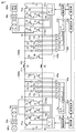
- FIG. 17 is a diagram showing a power conversion system according to a ninth embodiment.
- the power conversion device 1000a receives alternating current generated power from natural energy from a generator and performs high voltage direct current transmission.
- the power conversion device 1000b receives high voltage DC power from a submarine cable or the like and transmits the power to the power system.
- circuit configurations of power conversion device 1000a and power conversion device 1000b are the same as the circuit configuration of power conversion device 1000 of the eighth embodiment.
- the power converter 1000a is connected to the generator 980a via the grid relay 90a and the transformer 76a.
- Power converter 1000b is connected to transmission system 980b via system relay 90b and transformer 76b.
- Power conversion device 1000a and power conversion device 1000b are connected by DC circuit breakers 91a and 91b and DC power transmission cables 8a and 8b.
- the communication devices 80a and 80b can communicate not only with the power conversion device 1000a and the power conversion device 1000b, but also with external devices and communication infrastructure. This enables remote operation state monitoring, remote operation and the like.
- the power conversion device 1000a of the ninth embodiment carries out a test of a capacitor, the DC circuit breaker 91a and the system relay 90a are disconnected before the measurement is started.
- the measurement is started after the DC breaker 91b and the system relay 90b are disconnected.
- the first reason is to separate the potentials of PLa and PLb of the power conversion device 1000a and the power conversion device 1000b. Another reason is to prevent the parasitic inductance and parasitic capacitance of the DC power transmission cables 8a and 8b from becoming measurement errors during the capacitor test.
- the first reason is that the voltage fluctuation of the generator 980a inhibits the test of the capacitor. Another reason is that since the stored energy of the capacitor to be charged and discharged is large, unnecessary voltage fluctuation is not given to the generator 980a when the capacitor is tested.
- the first reason is that the voltage fluctuation of the transmission system 980b inhibits the capacitor test. Another reason is that since the stored energy of the capacitor to be charged and discharged is large, unnecessary voltage fluctuation is not given to the transmission system 980b when the capacitor is tested.
- the transformers 76a and 76b can take on the function of storing regenerative energy when the capacitor ripple test is performed.
- a submarine cable having a length of several tens of kilometers or more may be used as the DC power transmission cable 8a, 8b. It is common to check the submarine cable by pulling the submarine cable to the sea using a large vessel.
- the parasitic inductance of the DC power transmission cables 8a and 8b is several hundred ⁇ H or more. Therefore, it is possible to simplify the inspection of the cable by measuring in advance the capacitances of the test target capacitors 12a to 12c and performing the inductance measurement described later.
- FIG. 18 is a flowchart showing a procedure of measuring the parasitic inductance of the DC power transmission cable of the ninth embodiment.
- step S401 the power conversion devices 1000a and 1000b are shut down. All the switching elements 4a and 4b and the switching elements 5a to 5l are turned off.
- step S402 the system relay 90a and the system relay 90b are opened, the DC breaker 91b is closed, and the DC breaker 91a is kept open.
- step S403 the switching element 4a is turned on, and the power of the DC power supply 1a is used to fully charge the test target capacitors 12a to 12c. Next, the switching element 4a is turned off.
- step S404 the direct current circuit breaker 91a is closed, and temporal changes in voltage and current between the terminals of the capacitors 12a to 12c to be tested are measured using the A / D converter 17a and the control device 18.
- the DC circuit breaker 91a When the DC circuit breaker 91a is closed, charges accumulated in the test target capacitors 12a to 12c move to the test target capacitors 12d, 12e and 12f via the DC circuit breakers 91a and 91b and the DC power transmission cables 8a and 8b.
- the LC resonance starts between the parasitic inductances of the DC power transmission cables 8a and 8b and the test target capacitors 12d, 12e and 12f, and the current flowing through the test target capacitors 12d, 12e and 12f also oscillates at the oscillation frequency. This oscillation phenomenon is gradually attenuated by consuming energy by parasitic resistance in the circuit.
- step S405 the oscillation frequency of the current flowing to the capacitors under test 12a to 12c is obtained from the measurement result of step S404, and the inductance value is calculated from the result using the following equation (21) described later.
- the inductance value to be obtained is L (H)
- the combined capacitance of the capacitors 12a to 12c and 12d to 12f to be tested is C (F)
- the resonance frequency is f (Hz)
- the circling constant is .pi. It holds.
- the combined capacitance C of the test target capacitors increases. . That is, the combined capacitance is the sum of the capacitances of the test target capacitors 12d to 12e.
- a decrease in resonant frequency and an increase in current of the capacitors 12a to 12c to be tested occur. Therefore, a short circuit failure of the DC power transmission cables 8a and 8b is detected from the measurement results of the resonant frequency can do.
- the parasitic inductance L between the DC power transmission cables 8a and 8b changes according to the position where the DC power transmission cables 8a and 8b are short-circuited.
- a state in which the DC power transmission cables 8a and 8b are short-circuited at the power receiving end of the power conversion device 1000b is simulated to obtain an inductance value.
- the ratio La / Lb of the inductance La when the DC transmission cables 8a and 8b are actually short-circuited and the inductance Lb of the pseudo test is determined. If the distance between power conversion device 1000a and power conversion device 1000b is divided by the obtained inductance ratio (La / Lb), the cable length from power conversion device 1000a to the short circuit can be obtained.
- the failure recovery time of the power transmission cable can be shortened and the labor saving of the investigation can be realized.
- the switching element 4 and the switching elements 5a to 5l are desirably elements with small on-resistance and low loss, but MOSFETs or IGBTs or thyristors may be used, and the type is not limited as long as they have switching characteristics.
- the current detection resistors 13a to 13c may be replaced by other current measurement means such as a current sensor or a current transformer.
- the number of test target capacitors 12a to 12c and the current detection resistors 13a, 13b, and 13c of the power conversion device 1000a does not have to be three as shown in FIG. 17, and may be any number if it is one or more.
- the number of test target capacitors 12d, 12e, 12f and current detection resistors 13d, 13e, 13f of the power conversion device 1000b does not have to be three as shown in FIG. 17 and may be any number if it is one or more. .
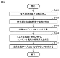
- FIG. 19 is a flow chart showing a control procedure of measurement of parasitic inductance of a wiring of the ninth embodiment.
- step S201 of FIG. 4 for fully charging the test target capacitor By changing step S201 of FIG. 4 for fully charging the test target capacitor to the control procedure of FIG. 18, it is possible to continuously test the parasitic inductance of the wiring and the capacitance measurement of the capacitor.
- step S501 the control device 18 turns off the switching element 4 of the switching element 4 and the charging circuit 200 through the gate driver 19 in order to discharge the residual charge of the test target capacitor 12.
- the control device 18 further turns on the switching element 14 of the discharge circuit 300 to discharge the residual charge of the test object capacitor 12 by the discharge resistor 15.
- control device 18 turns off the switching element 14 of the discharge circuit 300 through the gate driver 19.
- step S502 the control device 18 causes the measurement circuit 60 to start measurement of the combined current I1 of the test target capacitors 12a to 12c and the voltage V2 between XY.
- step S503 the control device 18 turns off the switching element 4 or the switching element 11 of the charging circuit 200 through the gate driver 19 to start charging the test object capacitor 12 in order to measure the parasitic inductance of the wiring.
- the charging resistor 10 needs charging It is desirable to have a resistance that allows current flow, an allowable loss, resistance accuracy, and a low parasitic inductance value.
- step S504 the control device 18 determines whether the test object capacitor 12 has reached full charge based on whether the measured combined current I1 and the voltage V2 between X and Y satisfy the predetermined condition. judge.
- control device 18 again measures the combined current I1 and the voltage V2 between XY, and then returns to step S504.
- step S504 when the test target capacitors 12a to 12c reach full charge, the control device 18 proceeds to the process of step S505.
- step S505 the control device 18 stops the measurement of the voltage V2 between the combined current I1 and XY of the test target capacitors 12a to 12c.
- step S506 the control device 18 calculates the parasitic inductance of the wiring by a method to be described later based on the temporal change of the voltage V2 between the test target capacitors 12a to 12c and the voltage V2 between XY.
- the stop of the power conversion device the adjustment of the ripple current at the capacitor test, the alarm display on the control panel 70, or the notification of abnormality to other devices by the communication device 80 Etc. may be performed.
- FIG. 20 is a diagram showing a voltage waveform between X and Y at the time of measuring a parasitic inductance of the wiring of the ninth embodiment and a waveform of a combined current I of a capacitor to be tested.
- the waveform 81 represents the voltage V0 between X and Y.
- the voltage V0 is a relative value that sets the full charge voltage of the test target capacitors 12a to 12c to one.
- the waveform 82 represents the combined current Ic of the capacitors under test 12a-12c.
- the combined current Ic is a relative value where the peak current on the + side is 1.
- the combined current Ic oscillates for a fixed time after the start of charging due to the influence of the parasitic inductance of the wiring. The convergence time and amplitude of the vibration change depending on the capacitances of the capacitors 12a to 12c to be tested, the equivalent series resistance, the parasitic inductance of the wiring, the wiring resistance, and the power supply impedance.
- a waveform 83 is an excess voltage VP of V0 with respect to the full charge voltage of the capacitors 12a to 12c to be tested.
- Overvoltage VP oscillates for a fixed time after the start of charging due to the influence of the parasitic inductance of the wiring.
- the convergence time and amplitude of the vibration change depending on the capacitances of the capacitors 12a to 12c to be tested, the equivalent series resistance, the parasitic inductance of the wiring, the wiring resistance, and the power supply impedance.
- the voltage V0 between XY is 0 V
- the combined current Ic of the test target capacitors 12a to 12c is also 0 [A].
- the rate of rise of the combined current Ic of the test target capacitors 12a to 12c with time is restricted by the influence of the parasitic inductance of the wiring.
- the parasitic inductance of the wiring can be determined by measuring the rate of rise of the combined current Ic with time.
- FIG. 21 is a diagram showing a voltage waveform between X and Y during measurement of parasitic inductance of wiring immediately after the start of charging of test target capacitors 12a to 12c of the ninth embodiment, and a waveform of combined current I of the test target capacitor. It is.
- the waveform of FIG. 21 expands the time region of a tenth to a few tenths of the charging time T with respect to the waveform of FIG.
- the waveform 91 represents the voltage V0 between X and Y.
- a waveform 92 is a combined current I of the capacitors 12a to 12c to be tested.
- the parasitic inductance L of the wiring The charging current increases substantially in proportion to the passage of time from the moment when charging of the capacitors 12a to 12c to be tested is started.
- the point Y is a point at which an arbitrary voltage ⁇ Vc is about 0 to 5% or less of the full charge voltage of the test target capacitors 12a to 12c in the voltage waveform between XY. If ⁇ Vc is set small, the linearity of the combined current I with time will increase and it will be easy to determine the inductance with high accuracy, but it will be difficult to obtain the measurement accuracy of the voltage. Therefore, it is desirable to select ⁇ Vc in consideration of the reciprocity of the linearity of the combined current I with time and the measurement accuracy of the voltage.
- ⁇ Tc is a charging time until the voltage between X and Y reaches an arbitrary voltage ⁇ Vc.
- the point Z is a point of the waveform 92 when ⁇ Tc has elapsed from the start of charging.
- ⁇ Ic is a combined current I of the capacitors under test 12a, 12b, 12 at Z.
- the parasitic inductance of the wiring is L
- the amount of increase in the charging current is ⁇ Ic
- the elapsed time from when the charging of the test object capacitors 12a to 12c starts charging to ⁇ Ic is ⁇ Tc
- the voltage of the DC power supply 1 is V
- the parasitic inductance L (unit: H) of the wiring can be obtained by the following equation.
- the control circuit determines the degree of deterioration of the test target capacitor based on the measured electrical characteristics, detects a failure and a sign of failure of the capacitor, and Realize failure avoidance by adjusting the output of converter
- the electric vehicle can move to a safe place while reducing the output of the mounted power conversion device to avoid failure.
- the detection of a failure sign can arrange replacement parts before the failure, the repair period can be shortened. Furthermore, since the failure of the power conversion device connected to the power system can be avoided, the power supply of the power infrastructure can be stabilized.
- tests of capacitors in these power conversion devices and the like can be performed in a short time (within several tens of microseconds to several hundreds of ms) using the standby state of the device (for example, when the electric vehicle is stopped). Alternatively, since the test can be performed while the device is in operation, the capacitor test does not have the disadvantage of impairing the convenience of the device.
- the capacitance and the equivalent series resistance are used as the electrical characteristics for determining the degree of deterioration, but other electrical characteristics may be used.
- it may be a parasitic inductance of a wire, a leak current, a dielectric loss tangent, a dielectric loss, a piezoelectric characteristic, or a resurrection voltage.
Landscapes
- Physics & Mathematics (AREA)
- General Physics & Mathematics (AREA)
- Engineering & Computer Science (AREA)
- Power Engineering (AREA)
- Manufacturing & Machinery (AREA)
- Microelectronics & Electronic Packaging (AREA)
- Testing Electric Properties And Detecting Electric Faults (AREA)
Abstract
La présente invention concerne un circuit de génération de courant d'ondulation (100) qui applique un courant d'ondulation à un condensateur (12) à tester. Un dispositif de commande (18) ajuste le courant d'ondulation sur la base d'un changement des caractéristiques électriques du condensateur à tester, et ajuste le courant d'ondulation qui est généré par le circuit de génération de courant d'ondulation (100) lorsqu'un test est poursuivi.
Applications Claiming Priority (2)
| Application Number | Priority Date | Filing Date | Title |
|---|---|---|---|
| JP2018010488 | 2018-01-25 | ||
| JP2018-010488 | 2018-01-25 |
Publications (1)
| Publication Number | Publication Date |
|---|---|
| WO2019146399A1 true WO2019146399A1 (fr) | 2019-08-01 |
Family
ID=67395955
Family Applications (1)
| Application Number | Title | Priority Date | Filing Date |
|---|---|---|---|
| PCT/JP2019/000292 Ceased WO2019146399A1 (fr) | 2018-01-25 | 2019-01-09 | Dispositif de test de condensateur, dispositif de conversion d'énergie électrique et procédé de test de condensateur |
Country Status (1)
| Country | Link |
|---|---|
| WO (1) | WO2019146399A1 (fr) |
Cited By (4)
| Publication number | Priority date | Publication date | Assignee | Title |
|---|---|---|---|---|
| JP2021148759A (ja) * | 2020-03-17 | 2021-09-27 | 株式会社 電子制御国際 | 耐電圧試験装置 |
| CN113991985A (zh) * | 2021-10-28 | 2022-01-28 | 湖南航天磁电有限责任公司 | Pwm全桥电机驱动中的突波吸收电路、实验平台及实验方法 |
| CN118818201A (zh) * | 2024-09-20 | 2024-10-22 | 四川省科学城久信科技有限公司 | 一种脉冲电容器测试装置及其测试方法 |
| CN119471066A (zh) * | 2025-01-08 | 2025-02-18 | 贵州送变电有限责任公司 | 一种高压频域介电谱测试系统及方法 |
Citations (11)
| Publication number | Priority date | Publication date | Assignee | Title |
|---|---|---|---|---|
| JPH02152216A (ja) * | 1988-12-05 | 1990-06-12 | Fujitsu Denso Ltd | コンデンサのエージング装置 |
| JPH0384477A (ja) * | 1989-08-28 | 1991-04-10 | Fujitsu Ltd | コンデンサ試験回路 |
| JP2002098725A (ja) * | 2000-09-27 | 2002-04-05 | Fuji Electric Co Ltd | コンデンサの良否判定装置 |
| JP2007155599A (ja) * | 2005-12-07 | 2007-06-21 | Nf Corp | 素子の試験装置 |
| KR20120031839A (ko) * | 2010-09-27 | 2012-04-04 | 손진근 | 직류/직류 컨버터를 이용한 직류 버스 커패시터의 간단한 등가직렬저항 측정 시스템 |
| KR20130042083A (ko) * | 2011-10-18 | 2013-04-26 | 손진근 | 전력변환기에 대한 직류링크 커패시터 장착형 커패시터 고장진단 통신 시스템 |
| KR101452724B1 (ko) * | 2014-07-28 | 2014-10-23 | 주식회사 뉴인텍 | 자동차 인버터용 커패시터의 리플 전류 시험 장치 및 방법 |
| CN105866554A (zh) * | 2015-01-19 | 2016-08-17 | 艾默生网络能源有限公司 | 一种直流母线电容的容值检测设备、方法及装置 |
| JP2017011263A (ja) * | 2015-06-25 | 2017-01-12 | ミツビシ・エレクトリック・アールアンドディー・センター・ヨーロッパ・ビーヴィMitsubishi Electric R&D Centre Europe B.V. | 電解コンデンサ状態をオンラインで監視する方法及びシステム |
| JP2018120987A (ja) * | 2017-01-26 | 2018-08-02 | 三菱電機株式会社 | コンデンサ試験装置 |
| JP6456578B1 (ja) * | 2017-11-10 | 2019-01-23 | 三菱電機株式会社 | 電力変換装置の試験システム及び試験方法 |
-
2019
- 2019-01-09 WO PCT/JP2019/000292 patent/WO2019146399A1/fr not_active Ceased
Patent Citations (11)
| Publication number | Priority date | Publication date | Assignee | Title |
|---|---|---|---|---|
| JPH02152216A (ja) * | 1988-12-05 | 1990-06-12 | Fujitsu Denso Ltd | コンデンサのエージング装置 |
| JPH0384477A (ja) * | 1989-08-28 | 1991-04-10 | Fujitsu Ltd | コンデンサ試験回路 |
| JP2002098725A (ja) * | 2000-09-27 | 2002-04-05 | Fuji Electric Co Ltd | コンデンサの良否判定装置 |
| JP2007155599A (ja) * | 2005-12-07 | 2007-06-21 | Nf Corp | 素子の試験装置 |
| KR20120031839A (ko) * | 2010-09-27 | 2012-04-04 | 손진근 | 직류/직류 컨버터를 이용한 직류 버스 커패시터의 간단한 등가직렬저항 측정 시스템 |
| KR20130042083A (ko) * | 2011-10-18 | 2013-04-26 | 손진근 | 전력변환기에 대한 직류링크 커패시터 장착형 커패시터 고장진단 통신 시스템 |
| KR101452724B1 (ko) * | 2014-07-28 | 2014-10-23 | 주식회사 뉴인텍 | 자동차 인버터용 커패시터의 리플 전류 시험 장치 및 방법 |
| CN105866554A (zh) * | 2015-01-19 | 2016-08-17 | 艾默生网络能源有限公司 | 一种直流母线电容的容值检测设备、方法及装置 |
| JP2017011263A (ja) * | 2015-06-25 | 2017-01-12 | ミツビシ・エレクトリック・アールアンドディー・センター・ヨーロッパ・ビーヴィMitsubishi Electric R&D Centre Europe B.V. | 電解コンデンサ状態をオンラインで監視する方法及びシステム |
| JP2018120987A (ja) * | 2017-01-26 | 2018-08-02 | 三菱電機株式会社 | コンデンサ試験装置 |
| JP6456578B1 (ja) * | 2017-11-10 | 2019-01-23 | 三菱電機株式会社 | 電力変換装置の試験システム及び試験方法 |
Cited By (4)
| Publication number | Priority date | Publication date | Assignee | Title |
|---|---|---|---|---|
| JP2021148759A (ja) * | 2020-03-17 | 2021-09-27 | 株式会社 電子制御国際 | 耐電圧試験装置 |
| CN113991985A (zh) * | 2021-10-28 | 2022-01-28 | 湖南航天磁电有限责任公司 | Pwm全桥电机驱动中的突波吸收电路、实验平台及实验方法 |
| CN118818201A (zh) * | 2024-09-20 | 2024-10-22 | 四川省科学城久信科技有限公司 | 一种脉冲电容器测试装置及其测试方法 |
| CN119471066A (zh) * | 2025-01-08 | 2025-02-18 | 贵州送变电有限责任公司 | 一种高压频域介电谱测试系统及方法 |
Similar Documents
| Publication | Publication Date | Title |
|---|---|---|
| CN112513651B (zh) | 用于检测绝缘故障的方法 | |
| JP5250220B2 (ja) | It給電系内の絶縁抵抗を測定する方法 | |
| EP3000646B2 (fr) | Système d'entraînement hybride | |
| US10640003B2 (en) | Double-pulse test systems and methods | |
| WO2019146399A1 (fr) | Dispositif de test de condensateur, dispositif de conversion d'énergie électrique et procédé de test de condensateur | |
| WO2014132321A1 (fr) | Dispositif source d'énergie | |
| KR102797069B1 (ko) | 차량 및 차량의 제어방법 | |
| JP5377636B2 (ja) | 電気的な負荷をシミュレーションするための回路 | |
| CN103444065B (zh) | 车辆的电源系统 | |
| EP2492700B1 (fr) | Système de test et procédé de test de bloc-batterie | |
| US9612998B2 (en) | Method and apparatus for motor drive diagnostics | |
| CN103308769A (zh) | 车载高电压设备的漏电电阻检测装置及漏电电阻检测方法 | |
| JPWO2018216208A1 (ja) | 電力変換装置 | |
| CN103119825A (zh) | 用于电动车辆的电池的dc充电站 | |
| CN112240988B (zh) | 电池监视系统和方法以及具有该电池监控系统的运输系统 | |
| JP2014519804A (ja) | 多電圧車載電源網を接続する装置および方法 | |
| JP2010252443A (ja) | 電気車用電力供給装置 | |
| JP2015006077A (ja) | 蓄電装置を搭載した電力変換装置 | |
| US12132384B2 (en) | Current measuring circuit for a converter, converter circuit and converter | |
| CN112335163A (zh) | 无源的滤波器电路的电容器功能的确定 | |
| JP5748610B2 (ja) | 充電装置 | |
| US20260084555A1 (en) | Charging device and method for operating the charging device | |
| EP1671143B1 (fr) | Procede et dispositif pour tester en direct une liaison intermediaire | |
| US10938302B2 (en) | Elimination of power inductor thermistor with variable air gap | |
| JP4391339B2 (ja) | 車両用補助電源装置 |
Legal Events
| Date | Code | Title | Description |
|---|---|---|---|
| 121 | Ep: the epo has been informed by wipo that ep was designated in this application |
Ref document number: 19744128 Country of ref document: EP Kind code of ref document: A1 |
|
| NENP | Non-entry into the national phase |
Ref country code: DE |
|
| 122 | Ep: pct application non-entry in european phase |
Ref document number: 19744128 Country of ref document: EP Kind code of ref document: A1 |
|
| NENP | Non-entry into the national phase |
Ref country code: JP |