WO2019193641A1 - Dispositif de communication sans fil - Google Patents
Dispositif de communication sans fil Download PDFInfo
- Publication number
- WO2019193641A1 WO2019193641A1 PCT/JP2018/014170 JP2018014170W WO2019193641A1 WO 2019193641 A1 WO2019193641 A1 WO 2019193641A1 JP 2018014170 W JP2018014170 W JP 2018014170W WO 2019193641 A1 WO2019193641 A1 WO 2019193641A1
- Authority
- WO
- WIPO (PCT)
- Prior art keywords
- signal
- unit
- frequency
- inverse system
- digital
- Prior art date
- Legal status (The legal status is an assumption and is not a legal conclusion. Google has not performed a legal analysis and makes no representation as to the accuracy of the status listed.)
- Ceased
Links
Images





Classifications
-
- H—ELECTRICITY
- H04—ELECTRIC COMMUNICATION TECHNIQUE
- H04B—TRANSMISSION
- H04B1/00—Details of transmission systems, not covered by a single one of groups H04B3/00 - H04B13/00; Details of transmission systems not characterised by the medium used for transmission
- H04B1/02—Transmitters
- H04B1/04—Circuits
-
- H—ELECTRICITY
- H04—ELECTRIC COMMUNICATION TECHNIQUE
- H04L—TRANSMISSION OF DIGITAL INFORMATION, e.g. TELEGRAPHIC COMMUNICATION
- H04L27/00—Modulated-carrier systems
- H04L27/32—Carrier systems characterised by combinations of two or more of the types covered by groups H04L27/02, H04L27/10, H04L27/18 or H04L27/26
- H04L27/34—Amplitude- and phase-modulated carrier systems, e.g. quadrature-amplitude modulated carrier systems
- H04L27/36—Modulator circuits; Transmitter circuits
Definitions
- the present invention relates to a wireless communication apparatus including a quadrature modulator.
- a baseband IQ (In-phase Quadrature) signal is defined, and the baseband IQ signal is up-converted by quadrature modulation.
- quadrature modulation schemes such as 64QAM (Quadrature Amplitude Modulation).
- Patent Document 1 a transmission signal in operation is input to a quadrature modulator of an analog circuit, a signal output from the quadrature modulator of the analog circuit is input to a digital quadrature detector, and a signal output from the digital quadrature detector A method of correcting the above with a digital circuit is disclosed.
- the method described in Patent Document 1 uses the inverse system of the identified system to identify the characteristics of the quadrature modulator when the digital circuit corrects an error that occurs when the quadrature modulator of the analog circuit is used.
- the IQ baseband signal is corrected.
- the present invention has been made in view of the above, and an object of the present invention is to obtain a wireless communication apparatus that suppresses distortion due to the characteristics of a quadrature modulator.
- a wireless communication device includes a calibration signal generation unit that generates a first signal in which a power spectrum on a frequency axis has a comb shape, A quadrature modulation unit that modulates one signal, an inverse system identification unit that identifies an inverse system of the quadrature modulation unit using the first signal, and correction of distortion generated in the quadrature modulation unit using the identified inverse system
- a first signal is orthogonal to a signal obtained by inverting the frequency of the first signal.
- the wireless communication apparatus has an effect that distortion due to the characteristics of the quadrature modulator can be suppressed.
- wireless communication apparatus concerning embodiment The figure which shows the functional block of the calibration signal generation part concerning embodiment
- the figure which shows the functional block of the orthogonal modulation part concerning embodiment The figure which shows the functional block of the digital quadrature demodulation part concerning embodiment
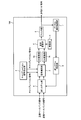
- FIG. 1 is a diagram illustrating a wireless communication apparatus according to an embodiment.
- the wireless communication apparatus 100 includes a calibration signal generation unit 1, a signal selection unit 2, a DA conversion unit 3a, a DA conversion unit 3b, an orthogonal modulation unit 4, an oscillation unit 5, a filter unit 6, and a digital orthogonal A demodulation unit 7, an inverse system identification unit 8, and an inverse system unit 9 are provided.
- the wireless communication device 100 operates at the time of calibration, that is, when detecting the characteristic of the quadrature modulation unit 4 and correcting an error caused by the characteristic, and at the time of normal transmission, that is, when transmitting the transmission baseband signals I and Q. Is different.
- the calibration signal generation unit 1 transmits calibration signals I and Q to the signal selection unit 2.
- the calibration signals I and Q are also called first signals.
- the signal selection unit 2 transmits the calibration signals I and Q to the DA conversion unit 3a and the DA conversion unit 3b, respectively.
- the DA conversion unit 3a and the DA conversion unit 3b convert a digital calibration signal into an analog calibration signal.
- the reason for having two DA converters is to express a spectrum which is positive and negative asymmetric between the I signal and the Q signal as a complex number.
- the quadrature modulation unit 4 mixes the calibration signal I with the RF carrier sine wave oscillated by the oscillation unit 5.
- the quadrature modulation unit 4 mixes the calibration signal Q and the RF carrier sine wave including the 90-degree phase offset oscillated by the oscillation unit 5.
- the calibration signals I and Q are up-converted by the mixing of the quadrature modulation unit 4.
- a signal generated by the oscillator 5 is also called a local signal.
- the filter unit 6 performs frequency filtering on the up-converted calibration signals I and Q, removes unnecessary high frequency components higher than the threshold included in the calibration signals I and Q, and outputs an IF signal or an RF signal. Output.
- the filter unit 6 is a BPF (Band Pass Filter). In the present embodiment, the threshold value is not particularly limited.
- the digital quadrature demodulator 7 converts the IF signal or RF signal into digital baseband signals I and Q.
- the inverse system identification unit 8 identifies the inverse system using the digital baseband signals I and Q.
- the inverse system unit 9 corrects the distortion generated in the orthogonal modulation unit 4 by multiplying the baseband signals I and Q by the matrix indicating the inverse system calculated by the inverse system identification unit 8.
- the inverse system unit 9 is also called a correction unit.
- the inverse system unit 9 receives the transmission baseband signals I and Q.
- the inverse system unit 9 adds an inverse characteristic that is an inverse characteristic of the characteristic of the orthogonal modulation unit 4 to the transmission baseband signals I and Q.
- the signal selection unit 2 transmits the transmission baseband signals I and Q output from the inverse system unit 9 to the DA conversion units 3a and 3b, respectively.
- the quadrature modulation unit 4 mixes and up-converts the outputs of the DA conversion units 3a and 3b and the output of the oscillation unit 5.
- the filter unit 6 performs frequency filtering and outputs an IF signal or an RF signal.
- the wireless communication apparatus 100 can perform transmission in which the distortion of the orthogonal modulation unit 4 is corrected during normal transmission.
- FIG. 2 is a diagram illustrating functional blocks of the calibration signal generation unit 1 according to the embodiment.
- the calibration signal generator 1 includes a base signal memory 11, a counter 12, a numerical controller 13, and a complex multiplier 14.
- FIG. 3 is a diagram illustrating the power spectrum of the base signal stored in the base signal memory 11 according to the embodiment.
- the base signal memory 11 stores a time domain signal of the frequency domain power spectrum shown in FIG. 3 as a base signal.
- a signal for each subcarrier is represented by a complex number C m (m is an integer).
- the base signal has power in all subcarriers.
- the base signal memory 11 repeatedly outputs the base signal shown in FIG. 3 a times by sweeping the memory address from the counter 12. By repeatedly outputting the base signal a times, a spectrum of a intervals in terms of the number of subcarriers is obtained.
- the numerical control unit 13 is also called an NCO (Numerical Controlled Oscillator).
- the complex multiplier 14 offsets (shifts) the frequency, performs convolution in the frequency domain, and obtains the power spectrum of the calibration signal.
- the base signal is preferably a signal having a small envelope variation such as a ZC (Zadoff Chu) series, but is not particularly limited as long as the frequency characteristic is a signal whose amplitude is not 0 for each subcarrier.
- j represents an imaginary unit
- F represents a signal sample rate F [Hz].
- K is an integer of 1 or more and less than a / 2.
- k is calculated by the following equation (3).
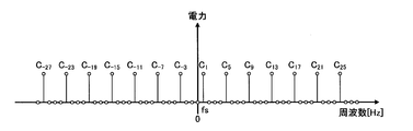
- FIG. 4 is a diagram illustrating an example of a power spectrum output from the calibration signal generation unit 1 according to the embodiment.
- the output of the calibration signal generation unit 1, sub-carrier interval is impulse-like spectrum of f s [Hz] interval.
- the frequency f i [Hz] of each subcarrier is calculated as shown in Equation (2).
- f i f s ⁇ i (2)
- the sub-carrier interval between C 1 and C 5 is a 4f s.
- i is an integer of ⁇ n to n, and the total number of subcarriers is 2n + 1.
- subcarriers that satisfy Equation (3) have power.
- a subcarrier that does not satisfy Equation (3) has no power and a value of zero.
- i mod a k (3)
- a is a constant.
- a is an integer of 3 or more.
- a signal for each subcarrier is represented by a complex number C m (m is an integer).
- C m is an integer.
- i a ⁇ m + k (4)
- the calibration signal defined by Equation (2), Equation (3), and Equation (4) becomes a comb-shaped power spectrum on the frequency axis.
- the calibration signal when the positive / negative frequency is inverted to offset the subcarrier frequency, the calibration signal always overlaps the 0 portion of the signal before the inversion. That is, the calibration signal has a power spectrum with a regular interval of a satisfying Expression (3) such that the power spectrum in which the positive and negative frequencies are inverted overlaps the portion where the power spectrum of the signal before the inversion is zero. For this reason, the radio communication apparatus 100 can easily separate the error generated due to the characteristic of the orthogonal modulation unit 4 and the calibration signal.
- the calibration signal has a power spectrum with an equal interval of a satisfying the equation (3) so that the power spectrum obtained by reversing the positive and negative frequencies overlaps the portion where the power spectrum of the signal before the reversal is zero.
- the generation method is not particularly limited.
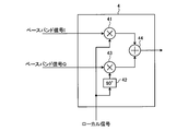
- FIG. 5 is a diagram illustrating functional blocks of the orthogonal modulation unit 4 according to the embodiment.
- the quadrature modulation unit 4 includes a multiplier 41, a phase shifter 42, a multiplier 43, and an adder 44.
- the multiplier 41 multiplies the local signal output from the oscillation unit 5 and the baseband signal I.
- the phase shifter 42 includes a 90 ° phase offset in the local signal.
- the multiplier 43 multiplies the local signal output from the phase shifter 42 and the baseband signal Q.
- the adder 44 adds the signal output from the multiplier 41 and the signal output from the multiplier 43.
- a series of operations performed by the multiplier 41, the phase shifter 42, the multiplier 43, and the adder 44 is called quadrature modulation.
- the signal handled by the quadrature modulation unit 4 is an analog signal.
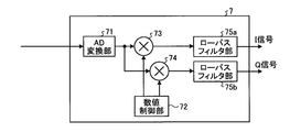
- FIG. 6 is a diagram illustrating functional blocks of the digital quadrature demodulation unit 7 according to the embodiment.
- the digital orthogonal demodulation unit 7 includes an AD conversion unit 71, a numerical control unit 72, a multiplier 73, a multiplier 74, a low-pass filter unit 75a, and a low-pass filter unit 75b.
- the AD converter 71 converts the IF signal or the RF signal into a digital signal. When converting, the AD converter 71 needs to convert at a sufficiently high sample rate so that waveform distortion due to aliasing does not occur.
- the numerical controller 72 generates a complex signal having a carrier frequency fc and outputs the complex signal to the multiplier 73.
- the numerical controller 72 outputs a complex signal including a 90 ° phase offset to the multiplier 74.
- the multiplier 73 multiplies the digital signal and the complex signal and outputs the result to the low-pass filter unit 75a.
- the multiplier 74 multiplies the digital signal by the complex signal including the 90 ° phase offset and outputs the result to the low-pass filter unit 75b.
- Low-pass filter sections 75a and 75b remove unnecessary frequency components and output baseband signals I and Q, respectively. Since the digital quadrature demodulator 7 performs all frequency conversion by digital processing, no quadrature error occurs.
- Calibration signal generation unit 1, signal selection unit 2, DA conversion unit 3a, DA conversion unit 3b, quadrature modulation unit 4, oscillation unit 5, filter unit 6, digital quadrature demodulation unit 7, inverse system identification unit according to the embodiment 8 and the inverse system unit 9 are realized by a processing circuit which is an electronic circuit for performing each processing.
- the processing circuit may be dedicated hardware or a control circuit including a memory and a CPU (Central Processing Unit) that executes a program stored in the memory.
- the memory corresponds to, for example, a nonvolatile or volatile semiconductor memory such as a RAM (Random Access Memory), a ROM (Read Only Memory), or a flash memory, a magnetic disk, or an optical disk.
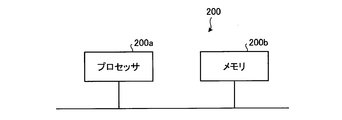
- the control circuit is, for example, a control circuit 200 having a configuration shown in FIG.
- the control circuit 200 includes a processor 200a that is a CPU and a memory 200b.
- a processor 200a that is a CPU
- a memory 200b When realized by the control circuit 200 shown in FIG. 7, it is realized by the processor 200a reading and executing a program corresponding to each process stored in the memory 200b.
- the memory 200b is also used as a temporary memory in each process performed by the processor 200a.
- FIG. 8 is a diagram illustrating a method for modeling an error generated in the orthogonal modulation unit 4 according to the embodiment.
- Inputs, filters, and outputs are all represented in complex numbers.
- the distortion generated in the quadrature modulation unit 4 can be modeled by the fact that the quadrature error and the error generated due to imbalance between the amplitude levels of the I axis and the Q axis have frequency characteristics. In this case, these errors appear as spectral inversion components on the frequency axis. These errors can be expressed using complex conjugates on the time axis.
- radio communication apparatus 100 can model an error generated in quadrature modulation unit 4 by performing system identification using x (t) and y (t).
- t shown in x (t) and y (t) represents time.
- Equation (5) is obtained.
- Y (f) H 1 (f) X (f) + H 2 (f) X ( ⁇ f) * (5)
- f is the frequency
- * represents a complex conjugate.
- the complex conjugate of y (t) is converted to the frequency axis to obtain Equation (6).
- Y ( ⁇ f) * H2 ( ⁇ f) * X (f) + H1 ( ⁇ f) * X ( ⁇ f) * ... (6)
- Equation (7) is obtained.
- X (f) is calculated by equation (8) using an inverse matrix.
- E (f) H 1 (f) H 1 ( ⁇ f) * ⁇ H 2 (f) H 2 ( ⁇ f) * (9)
- the inverse system on the frequency axis can be calculated by Expression (10). Since the output of the calibration signal generator 1 and the frequency determination component are easily separated, H 1 and H 2 can be obtained with high accuracy.
- FIG. 9 is a functional block diagram of the inverse system identification unit 8 according to the embodiment.
- the inverse system identification unit 8 includes a Fourier transform unit 81, a main signal identification unit 82, a frequency identification unit 83, and an inverse system calculation unit 84.
- the Fourier transform unit 81 transforms the output of the digital quadrature demodulation unit 7 into a frequency axis by FFT (Fast Fourier Transform).
- the main signal identification unit 82 extracts a subcarrier signal.
- the frequency identification unit 83 extracts a subcarrier signal whose frequency is inverted.
- the main signal identifying unit 82 and the frequency identifying unit 83 perform system identification for each subcarrier by dividing the base signal corresponding to each extracted signal by a complex number.
- a plurality of measurements may be performed, and the measurement results may be averaged and averaged as a system identification result.
- interpolation processing in the frequency direction may be performed during system identification.
- the inverse system calculation unit 84 uses the H 1 (f) and H 2 (f) calculated by the main signal identification unit 82 and the frequency identification unit 83, respectively, to calculate the inverse system on the frequency axis represented by Expression (10). Calculate and output frequency characteristics.
- FIG. 10 is a diagram illustrating functional blocks of the inverse system unit 9 according to the embodiment.
- FIG. 11 is a simplified representation of the inverse system unit 9 according to the embodiment.
- the inverse system unit 9 includes transversal filter units 91-1 to 91-p, an adder 92, and an adder 93.
- the inverse system unit 9 includes a p-stage transversal filter.
- the transversal filter can be represented by the four real filters shown in FIG.
- the tap coefficients of filter_a in FIG. 11 are a 0 to a p ⁇ 1 shown in FIG.
- the tap coefficients of filter_b are b 0 to b p ⁇ 1 shown in FIG.
- the tap coefficients of filter_c are c 0 to c p ⁇ 1 shown in FIG.
- the tap coefficients of filter_d are d 0 to d p ⁇ 1 shown in FIG. Those representing these four filters in the frequency axis A (f), B (f ), C (f), and when the D (f) These, H 1, and H of the inverse system identification unit 8 has determined 2 is used to calculate from Equations (11) to (14).
- a (f) (H 1I (f) ⁇ H 2I (f))) / E (f) (11)
- B (f) (H 1Q (f) ⁇ H 2Q (f)) / E (f) (12)
- C (f) ( ⁇ H 1Q (f) ⁇ H 2Q (f)) / E (f) (13)
- D (f) (H 1I (f) + H 2I (f)) / E (f) (14)
- Expressions (11) to (14) are all represented by real numbers.
- tap coefficients a 0 to a p ⁇ 1 , b 0 to b p ⁇ 1 , and c 0 to c p ⁇ 1 shown in FIG. And d 0 to d p ⁇ 1 can be obtained.
- Fourier transform may be performed.
- F + represents a general inverse matrix of F, and calculated a, b, c, and d are solutions of the least square method. Note that Equation (15) to Equation (18) may be further expanded to use a weighted least square method.
- the calibration signal generator 1 generates a calibration signal.
- the quadrature modulation unit 4 modulates using the calibration signal.
- the DA conversion unit 3a and the DA conversion unit 3b convert a digital calibration signal into an analog calibration signal.
- the filter unit 6 performs frequency filtering on the up-converted calibration signals I and Q, removes unnecessary high frequency components included in the calibration signals I and Q, and outputs an IF signal or an RF signal.
- the digital quadrature demodulation unit 7 demodulates the IF signal or the RF signal by digital processing, and the inverse system identification unit 8 uses the demodulated signal to identify the inverse system, thereby generating the characteristics of the quadrature modulation unit 4. Calculate the error.
- the inverse system unit 9 multiplies the transmission baseband signal by the inverse characteristic of the orthogonal modulation unit 4 using the calculated inverse system. By applying an inverse characteristic to the transmission baseband signal by the inverse system unit 9 and correcting an error caused by the characteristic of the quadrature modulation unit 4, distortion due to the characteristic of the quadrature modulator 4 can be suppressed.
- the configuration described in the above embodiment shows an example of the contents of the present invention, and can be combined with another known technique, and can be combined with other configurations without departing from the gist of the present invention. It is also possible to omit or change the part.
- 1 calibration signal generation unit 1 calibration signal generation unit, 2 signal selection unit, 3a, 3b DA conversion unit, 4 orthogonal modulation unit, 5 oscillation unit, 6 filter unit, 7 digital quadrature demodulation unit, 8 inverse system identification unit, 9 inverse system unit, 11 Base signal memory, 12 counter, 13, 72 numerical control unit, 14 complex multiplier, 41, 43, 73, 74 multiplier, 42 phase shifter, 44, 92, 93 adder, 71 AD conversion unit, 75a, 75b low pass Filter unit, 81 Fourier transform unit, 82 Main signal identification unit, 83 Frequency identification unit, 84 Inverse system calculation unit, 91-1 to 91-p transversal filter unit, 100 Wireless communication device, 200 Control circuit, 200a processor, 200b memory.
Landscapes
- Engineering & Computer Science (AREA)
- Computer Networks & Wireless Communication (AREA)
- Signal Processing (AREA)
- Digital Transmission Methods That Use Modulated Carrier Waves (AREA)
- Transmitters (AREA)
Abstract
Un dispositif de communication sans fil (100) selon la présente invention est caractérisé en ce qu'il est pourvu d'une unité de génération de signal d'étalonnage (1) destinée à générer un premier signal pour lequel le spectre de puissance sur un axe de fréquence est en forme de peigne, une unité de modulation en quadrature (4) destinée à moduler le premier signal, une unité d'identification de système inverse (8) destinée à identifier un système inverse de l'unité de modulation en quadrature à l'aide du premier signal, et une unité de système inverse (9) destinée à corriger une distorsion se produisant dans l'unité de modulation en quadrature à l'aide du système inverse identifié, et est en outre caractérisé en ce que le premier signal est orthogonal à un signal dans lequel la fréquence du premier signal est inversée.
Priority Applications (1)
| Application Number | Priority Date | Filing Date | Title |
|---|---|---|---|
| PCT/JP2018/014170 WO2019193641A1 (fr) | 2018-04-02 | 2018-04-02 | Dispositif de communication sans fil |
Applications Claiming Priority (1)
| Application Number | Priority Date | Filing Date | Title |
|---|---|---|---|
| PCT/JP2018/014170 WO2019193641A1 (fr) | 2018-04-02 | 2018-04-02 | Dispositif de communication sans fil |
Publications (1)
| Publication Number | Publication Date |
|---|---|
| WO2019193641A1 true WO2019193641A1 (fr) | 2019-10-10 |
Family
ID=68100184
Family Applications (1)
| Application Number | Title | Priority Date | Filing Date |
|---|---|---|---|
| PCT/JP2018/014170 Ceased WO2019193641A1 (fr) | 2018-04-02 | 2018-04-02 | Dispositif de communication sans fil |
Country Status (1)
| Country | Link |
|---|---|
| WO (1) | WO2019193641A1 (fr) |
Cited By (1)
| Publication number | Priority date | Publication date | Assignee | Title |
|---|---|---|---|---|
| WO2022201764A1 (fr) * | 2021-03-22 | 2022-09-29 | 日本電気株式会社 | Dispositif de traitement de signal, dispositif de communication sans fil, procédé de traitement de signal et support lisible par ordinateur non transitoire sur lequel est stocké un programme |
Citations (4)
| Publication number | Priority date | Publication date | Assignee | Title |
|---|---|---|---|---|
| JP2008283288A (ja) * | 2007-05-08 | 2008-11-20 | Toshiba Corp | 無線送信装置及び方法 |
| JP2009117897A (ja) * | 2007-11-01 | 2009-05-28 | Toshiba Corp | 無線送信装置および無線送信方法 |
| JP2011512770A (ja) * | 2008-02-19 | 2011-04-21 | サムスン エレクトロニクス カンパニー リミテッド | 直交周波数分割多重の受信機におけるi/q不均衡パラメーターを推定する装置及びその方法 |
| JP2012044236A (ja) * | 2010-08-12 | 2012-03-01 | Nippon Telegr & Teleph Corp <Ntt> | 送信機および送信方法 |
-
2018
- 2018-04-02 WO PCT/JP2018/014170 patent/WO2019193641A1/fr not_active Ceased
Patent Citations (4)
| Publication number | Priority date | Publication date | Assignee | Title |
|---|---|---|---|---|
| JP2008283288A (ja) * | 2007-05-08 | 2008-11-20 | Toshiba Corp | 無線送信装置及び方法 |
| JP2009117897A (ja) * | 2007-11-01 | 2009-05-28 | Toshiba Corp | 無線送信装置および無線送信方法 |
| JP2011512770A (ja) * | 2008-02-19 | 2011-04-21 | サムスン エレクトロニクス カンパニー リミテッド | 直交周波数分割多重の受信機におけるi/q不均衡パラメーターを推定する装置及びその方法 |
| JP2012044236A (ja) * | 2010-08-12 | 2012-03-01 | Nippon Telegr & Teleph Corp <Ntt> | 送信機および送信方法 |
Cited By (4)
| Publication number | Priority date | Publication date | Assignee | Title |
|---|---|---|---|---|
| WO2022201764A1 (fr) * | 2021-03-22 | 2022-09-29 | 日本電気株式会社 | Dispositif de traitement de signal, dispositif de communication sans fil, procédé de traitement de signal et support lisible par ordinateur non transitoire sur lequel est stocké un programme |
| JPWO2022201764A1 (fr) * | 2021-03-22 | 2022-09-29 | ||
| JP7619437B2 (ja) | 2021-03-22 | 2025-01-22 | 日本電気株式会社 | 信号処理装置、無線通信装置、信号処理方法及びプログラム |
| US12526059B2 (en) | 2021-03-22 | 2026-01-13 | Nec Corporation | Signal processing apparatus, radio communication apparatus, signal processing method, and non-transitory computer readable medium on which program is stored |
Similar Documents
| Publication | Publication Date | Title |
|---|---|---|
| US11296739B2 (en) | Noise suppression device, noise suppression method, and reception device and reception method using same | |
| US11258521B2 (en) | Front-end circuit | |
| CN115882970A (zh) | 一种接收iq不平衡校正方法及系统 | |
| Rampa | I/Q compensation of broadband direct-conversion transmitters | |
| CN103119871A (zh) | 确定信号路径属性的技术和测试信号 | |
| US20180083661A1 (en) | Wideband Residual Sideband Calibration | |
| CN114465677A (zh) | 校正宽带系统i/q不平衡的方法、宽带系统和介质 | |
| JP7111973B2 (ja) | 波長分散量推定装置 | |
| JP2012095120A (ja) | 測定装置、測定方法およびプログラム | |
| CN107819720A (zh) | Iq不平衡补偿方法和装置、时域补偿器及通信设备 | |
| JP5113677B2 (ja) | 位相差対応値測定装置、ゲインインバランス測定装置、方法、プログラムおよび記録媒体 | |
| JP2003188747A (ja) | 歪補償送信装置 | |
| JP5684771B2 (ja) | 変調信号解析装置および変調信号解析方法 | |
| KR20130056395A (ko) | 다이렉트 업컨버전 시스템에서 i/q 불균형 측정 장치 및 방법 | |
| CN117081684A (zh) | 非线性系统噪声的测量装置及方法 | |
| JP6381494B2 (ja) | 受信機および誤差補正方法 | |
| JP6902259B2 (ja) | 測定装置及び測定方法 | |
| JP3642471B2 (ja) | 伝送信号の生成方法、及び伝送信号の生成装置 | |
| JP5013613B2 (ja) | 直交変調・復調装置、直交変調器および直交復調器 | |
| JP4284770B2 (ja) | 直交周波数分割多重復調方法及び直交周波数分割多重復調装置 | |
| JP2504755B2 (ja) | 周波数オフセツトおよびジツタ印加回路 | |
| JP2025530199A (ja) | 単側波帯位相敏感検出方法及びシステム | |
| JP2000261401A (ja) | 直交変調方法、直交変調装置及び記録媒体 | |
| JP2003169034A (ja) | 行列・逆行列を利用した変調・復調装置 | |
| JP3331462B2 (ja) | Psk受信機 |
Legal Events
| Date | Code | Title | Description |
|---|---|---|---|
| 121 | Ep: the epo has been informed by wipo that ep was designated in this application |
Ref document number: 18913559 Country of ref document: EP Kind code of ref document: A1 |
|
| NENP | Non-entry into the national phase |
Ref country code: DE |
|
| 122 | Ep: pct application non-entry in european phase |
Ref document number: 18913559 Country of ref document: EP Kind code of ref document: A1 |
|
| NENP | Non-entry into the national phase |
Ref country code: JP |