WO2020003518A1 - 表示装置 - Google Patents
表示装置 Download PDFInfo
- Publication number
- WO2020003518A1 WO2020003518A1 PCT/JP2018/024903 JP2018024903W WO2020003518A1 WO 2020003518 A1 WO2020003518 A1 WO 2020003518A1 JP 2018024903 W JP2018024903 W JP 2018024903W WO 2020003518 A1 WO2020003518 A1 WO 2020003518A1
- Authority
- WO
- WIPO (PCT)
- Prior art keywords
- voltage
- display device
- gate
- inductor
- power supply
- Prior art date
- Legal status (The legal status is an assumption and is not a legal conclusion. Google has not performed a legal analysis and makes no representation as to the accuracy of the status listed.)
- Ceased
Links
Images


Classifications
-
- G—PHYSICS
- G09—EDUCATION; CRYPTOGRAPHY; DISPLAY; ADVERTISING; SEALS
- G09G—ARRANGEMENTS OR CIRCUITS FOR CONTROL OF INDICATING DEVICES USING STATIC MEANS TO PRESENT VARIABLE INFORMATION
- G09G3/00—Control arrangements or circuits, of interest only in connection with visual indicators other than cathode-ray tubes
- G09G3/20—Control arrangements or circuits, of interest only in connection with visual indicators other than cathode-ray tubes for presentation of an assembly of a number of characters, e.g. a page, by composing the assembly by combination of individual elements arranged in a matrix no fixed position being assigned to or needed to be assigned to the individual characters or partial characters
- G09G3/34—Control arrangements or circuits, of interest only in connection with visual indicators other than cathode-ray tubes for presentation of an assembly of a number of characters, e.g. a page, by composing the assembly by combination of individual elements arranged in a matrix no fixed position being assigned to or needed to be assigned to the individual characters or partial characters by control of light from an independent source
- G09G3/36—Control arrangements or circuits, of interest only in connection with visual indicators other than cathode-ray tubes for presentation of an assembly of a number of characters, e.g. a page, by composing the assembly by combination of individual elements arranged in a matrix no fixed position being assigned to or needed to be assigned to the individual characters or partial characters by control of light from an independent source using liquid crystals
- G09G3/3611—Control of matrices with row and column drivers
- G09G3/3674—Details of drivers for scan electrodes
-
- G—PHYSICS
- G09—EDUCATION; CRYPTOGRAPHY; DISPLAY; ADVERTISING; SEALS
- G09G—ARRANGEMENTS OR CIRCUITS FOR CONTROL OF INDICATING DEVICES USING STATIC MEANS TO PRESENT VARIABLE INFORMATION
- G09G3/00—Control arrangements or circuits, of interest only in connection with visual indicators other than cathode-ray tubes
- G09G3/20—Control arrangements or circuits, of interest only in connection with visual indicators other than cathode-ray tubes for presentation of an assembly of a number of characters, e.g. a page, by composing the assembly by combination of individual elements arranged in a matrix no fixed position being assigned to or needed to be assigned to the individual characters or partial characters
- G09G3/34—Control arrangements or circuits, of interest only in connection with visual indicators other than cathode-ray tubes for presentation of an assembly of a number of characters, e.g. a page, by composing the assembly by combination of individual elements arranged in a matrix no fixed position being assigned to or needed to be assigned to the individual characters or partial characters by control of light from an independent source
- G09G3/36—Control arrangements or circuits, of interest only in connection with visual indicators other than cathode-ray tubes for presentation of an assembly of a number of characters, e.g. a page, by composing the assembly by combination of individual elements arranged in a matrix no fixed position being assigned to or needed to be assigned to the individual characters or partial characters by control of light from an independent source using liquid crystals
- G09G3/3611—Control of matrices with row and column drivers
- G09G3/3674—Details of drivers for scan electrodes
- G09G3/3677—Details of drivers for scan electrodes suitable for active matrices only
-
- G—PHYSICS
- G02—OPTICS
- G02F—OPTICAL DEVICES OR ARRANGEMENTS FOR THE CONTROL OF LIGHT BY MODIFICATION OF THE OPTICAL PROPERTIES OF THE MEDIA OF THE ELEMENTS INVOLVED THEREIN; NON-LINEAR OPTICS; FREQUENCY-CHANGING OF LIGHT; OPTICAL LOGIC ELEMENTS; OPTICAL ANALOGUE/DIGITAL CONVERTERS
- G02F1/00—Devices or arrangements for the control of the intensity, colour, phase, polarisation or direction of light arriving from an independent light source, e.g. switching, gating or modulating; Non-linear optics
- G02F1/01—Devices or arrangements for the control of the intensity, colour, phase, polarisation or direction of light arriving from an independent light source, e.g. switching, gating or modulating; Non-linear optics for the control of the intensity, phase, polarisation or colour
- G02F1/13—Devices or arrangements for the control of the intensity, colour, phase, polarisation or direction of light arriving from an independent light source, e.g. switching, gating or modulating; Non-linear optics for the control of the intensity, phase, polarisation or colour based on liquid crystals, e.g. single liquid crystal display cells
- G02F1/133—Constructional arrangements; Operation of liquid crystal cells; Circuit arrangements
- G02F1/136—Liquid crystal cells structurally associated with a semi-conducting layer or substrate, e.g. cells forming part of an integrated circuit
- G02F1/1362—Active matrix addressed cells
- G02F1/136286—Wiring, e.g. gate line, drain line
-
- G—PHYSICS
- G02—OPTICS
- G02F—OPTICAL DEVICES OR ARRANGEMENTS FOR THE CONTROL OF LIGHT BY MODIFICATION OF THE OPTICAL PROPERTIES OF THE MEDIA OF THE ELEMENTS INVOLVED THEREIN; NON-LINEAR OPTICS; FREQUENCY-CHANGING OF LIGHT; OPTICAL LOGIC ELEMENTS; OPTICAL ANALOGUE/DIGITAL CONVERTERS
- G02F1/00—Devices or arrangements for the control of the intensity, colour, phase, polarisation or direction of light arriving from an independent light source, e.g. switching, gating or modulating; Non-linear optics
- G02F1/01—Devices or arrangements for the control of the intensity, colour, phase, polarisation or direction of light arriving from an independent light source, e.g. switching, gating or modulating; Non-linear optics for the control of the intensity, phase, polarisation or colour
- G02F1/13—Devices or arrangements for the control of the intensity, colour, phase, polarisation or direction of light arriving from an independent light source, e.g. switching, gating or modulating; Non-linear optics for the control of the intensity, phase, polarisation or colour based on liquid crystals, e.g. single liquid crystal display cells
- G02F1/133—Constructional arrangements; Operation of liquid crystal cells; Circuit arrangements
- G02F1/136—Liquid crystal cells structurally associated with a semi-conducting layer or substrate, e.g. cells forming part of an integrated circuit
- G02F1/1362—Active matrix addressed cells
- G02F1/1368—Active matrix addressed cells in which the switching element is a three-electrode device
-
- G—PHYSICS
- G09—EDUCATION; CRYPTOGRAPHY; DISPLAY; ADVERTISING; SEALS
- G09G—ARRANGEMENTS OR CIRCUITS FOR CONTROL OF INDICATING DEVICES USING STATIC MEANS TO PRESENT VARIABLE INFORMATION
- G09G2320/00—Control of display operating conditions
- G09G2320/02—Improving the quality of display appearance
- G09G2320/0223—Compensation for problems related to R-C delay and attenuation in electrodes of matrix panels, e.g. in gate electrodes or on-substrate video signal electrodes
-
- G—PHYSICS
- G09—EDUCATION; CRYPTOGRAPHY; DISPLAY; ADVERTISING; SEALS
- G09G—ARRANGEMENTS OR CIRCUITS FOR CONTROL OF INDICATING DEVICES USING STATIC MEANS TO PRESENT VARIABLE INFORMATION
- G09G2320/00—Control of display operating conditions
- G09G2320/02—Improving the quality of display appearance
- G09G2320/0252—Improving the response speed
-
- G—PHYSICS
- G09—EDUCATION; CRYPTOGRAPHY; DISPLAY; ADVERTISING; SEALS
- G09G—ARRANGEMENTS OR CIRCUITS FOR CONTROL OF INDICATING DEVICES USING STATIC MEANS TO PRESENT VARIABLE INFORMATION
- G09G2330/00—Aspects of power supply; Aspects of display protection and defect management
- G09G2330/02—Details of power systems and of start or stop of display operation
- G09G2330/021—Power management, e.g. power saving
- G09G2330/023—Power management, e.g. power saving using energy recovery or conservation
- G09G2330/024—Power management, e.g. power saving using energy recovery or conservation with inductors, other than in the electrode driving circuitry of plasma displays
-
- G—PHYSICS
- G09—EDUCATION; CRYPTOGRAPHY; DISPLAY; ADVERTISING; SEALS
- G09G—ARRANGEMENTS OR CIRCUITS FOR CONTROL OF INDICATING DEVICES USING STATIC MEANS TO PRESENT VARIABLE INFORMATION
- G09G2330/00—Aspects of power supply; Aspects of display protection and defect management
- G09G2330/02—Details of power systems and of start or stop of display operation
- G09G2330/025—Reduction of instantaneous peaks of current
Definitions
- the present invention relates to a display device having a plurality of pixels arranged along a plurality of rows and a plurality of columns.
- the resolution is further improved, such as FHD (Full High Definition), 4K, and 8K.
- FHD Full High Definition
- 4K 4K
- 8K 8K
- Patent Literature 1 discloses a liquid crystal display device that drives a liquid crystal element with an alternating current at a higher speed than in the related art, visually reduces interference noise of an adjacent wiring, and displays a high-quality image.
- the switching element of each pixel has a predetermined gate capacitance.
- a gate signal line connected to the gate of the switching element of each pixel has a predetermined resistance. Therefore, a CR circuit is formed from the gate capacitance of the switching element and the resistance of the signal line. When the switching element of each pixel is turned on or off, the CR circuit is charged or discharged.
- the CR circuit for example, when charging the CR circuit, a large current flows only at the moment when the power is turned on and the circuit is rapidly charged, but the charging speed gradually decreases, and the circuit reaches the potential of the power supply. It takes a long time to do. Also when discharging from a CR circuit, it takes a long time for the circuit to reach ground potential.
- the display device A plurality of pixels arranged along a plurality of rows and a plurality of columns, A plurality of signal lines respectively connected to the plurality of pixels for each row, A drive circuit that generates a plurality of control signals for selectively turning on and off the plurality of pixels for each row and applies the control signals to the signal lines; A power supply circuit that supplies a voltage for generating each of the control signals to the drive circuit; The power supply circuit and at least one inductor connected between the plurality of signal lines.
- the display device since the display device includes the inductor, the display device can operate at higher speed than the display device according to the related art, and can further reduce loss.
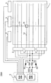
- FIG. 2 is a block diagram illustrating a configuration of a display device according to the first embodiment.
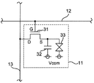
- FIG. 2 is a circuit diagram illustrating a detailed configuration of each pixel in FIG. 1.
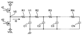
- FIG. 2 is an equivalent circuit diagram illustrating one of the gate signal lines in FIG. 1 and a plurality of pixels connected to the gate signal line.
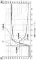
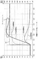
- 2 is a graph showing a change in voltage and current of a gate signal line when a gate control signal changes from a low level to a high level in one of the gate signal lines in FIG. 1.
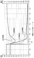
- 2 is a graph illustrating a change in voltage and current of a gate signal line when a gate control signal changes from a high level to a low level in one of the gate signal lines in FIG. 1.
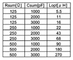
- FIG. 2 is a table showing optimum values of the inductance of the inductor of FIG. 1. It is a block diagram showing the composition of the display concerning a 2nd embodiment.
- 9 is a graph showing changes in voltage and current of a gate signal line when a gate control signal is changed from a low level to a high level in one of the gate signal lines of the display device according to the comparative example.
- 8 is a graph showing changes in voltage and current of a gate signal line when a gate control signal changes from a low level to a high level in one of the gate signal lines in FIG. 7.
- FIG. 1 is a block diagram illustrating a configuration of the display device 100 according to the first embodiment.
- the display device 100 includes a display panel 1, one or more gate drive circuits 2, one or more source drive circuits 3, a timing controller 4, and inductors L1 and L2.
- the display panel 1 includes a plurality of pixels 11 arranged in a row direction (horizontal direction in FIG. 1) and a column direction (vertical direction in FIG. 1), a plurality of gate signal lines 12 along a plurality of rows, and a plurality of gate signal lines 12. And a plurality of source signal lines 13 along the column.
- Each pixel 11 is connected to a gate signal line 12 and a source signal line 13, respectively.
- each pixel 11 is arranged along a plurality of rows and a plurality of columns, each gate signal line 12 is connected to a plurality of pixels 11 for each row, and each source signal line 13 is connected to a plurality of pixels for each column. 11 respectively.
- the display panel 1 is, for example, a liquid crystal panel.
- the gate drive circuit 2 generates a plurality of gate control signals for selectively turning on and off the plurality of pixels 11 for each row, and applies the generated signals to each gate signal line 12.
- a switching element (described later) inside the pixel 11 is turned on, and a capacitor and a display element inside the pixel 11 are connected to the source signal line 13.
- the source drive circuit 3 supplies a plurality of source control signals indicating the gradation of each pixel of the image along one of the plurality of rows to each pixel 11 via the plurality of source signal lines 13.
- the timing controller 4 includes a control circuit 21 and a power supply circuit 22.
- the control circuit 21 controls the gate drive circuit 2 and the source drive circuit 3.
- the power supply circuit 22 supplies voltages VGH and VGL for generating each gate control signal to the gate drive circuit 2.
- the voltage VGH is higher than the threshold voltage for turning on each pixel 11, and the voltage VGL is lower than the threshold voltage.
- the voltage VGH is also referred to as a “first voltage”
- the voltage VGL is also referred to as a “second voltage”.
- the inductances L1 and L2 are connected between the power supply circuit 22 and the plurality of gate signal lines 12, particularly, between the power supply circuit 22 and the gate drive circuit 22.
- the power supply circuit 22 supplies the voltage VGH to the gate drive circuit 22 via the inductor L1, and supplies the voltage VGL to the gate drive circuit 22 via the inductor L2.
- the inductor L1 is also referred to as a “first inductor”
- the inductor L2 is also referred to as a “second inductor”.
- FIG. 2 is a circuit diagram showing a detailed configuration of each pixel 11 in FIG.
- the pixel 11 includes a switching element 31, a capacitor 32, and a display element 33.
- the switching element 31 turns on and off according to the gate control signal.
- the switching element 31 is, for example, a thin film transistor.
- the capacitor 32 and the display element 33 are connected in parallel with each other, one end of which is connected to the source signal line 13 via the switching element 31, and the other end of which is connected to a terminal of a predetermined common voltage Vcom.
- the capacitor 32 is a capacitance element charged according to the voltage of the source control signal.
- the display element 33 has optical characteristics that change according to the voltage across the capacitor 32.
- the display element 33 is, for example, a liquid crystal.
- the gate control signal input from the gate drive circuit 2 to the display panel 1 propagates through the gate signal line 12 and is applied to the gate terminal of the switching element 31 of each pixel 11. Further, a source control signal input to the display panel 1 from the source driving circuit 3 propagates through the source signal line 13 and is applied to the drain terminal of the switching element 31 of each pixel 11.
- the switching element 31 is turned on, and conduction between the drain and source is made.
- the voltage of the source control signal applied to the drain terminal of the switching element 31 is supplied to the pixel 11 through the source terminal of the switching element 31, and the capacitor 32 is charged (or discharged) according to the voltage of the source control signal. ) Is done.
- FIG. 3 is an equivalent circuit diagram showing one of the gate signal lines 12 of FIG. 1 and a plurality of pixels 11 connected to the gate signal line 12.
- the gate drive circuit 2 includes switching elements 41 and 42 for selectively applying one of the voltages VGH and VGL to the gate signal line 12 for each gate signal line 12.
- Each of the switching elements 41 and 42 operates according to a control signal from the control circuit 21.
- R1 to RN indicate resistances of one gate signal line 12 itself.
- C1 to CN indicate the gate capacitance of the switching element 31 of each pixel 11 connected to one gate signal line 12.
- a CR circuit is formed from the gate capacitance of the switching element 31 of each pixel 11 and the resistance of the gate signal line 12. Due to this CR circuit, the time when the gate control signal transitions from a low level to a high level, or vice versa, becomes longer. Further, due to the CR circuit, when a voltage is applied to the gate capacitance to perform charging, energy consumed by the resistor is lost.
- the display device 100 according to the embodiment includes the inductors L1 and L2, and thus operates at a higher speed than the display device according to the related art, and further reduces loss, as described below.
- FIG. 4 is a graph showing changes in the voltage and current of the gate signal line 12 when the gate control signal is changed from a low level to a high level in one of the gate signal lines 12 of FIG.
- the voltage V1 approaches the potential of the voltage V0. It's been a long time. For example, assuming that the threshold voltage at which the switching element 31 of each pixel 11 is turned on is 32 V, the voltage V0 transitions to a high level and then 1.8 V from when the voltage V1 reaches 32 V (point B). It takes microseconds.
- the provision of the inductor L1 allows the voltage V1 to approach the potential of the voltage V0 in a shorter time than in the comparative example, after the voltage V0 transitions to the high level. For example, the time from when the voltage V0 transitions to the high level until the voltage V1 reaches 32 V (point A) is reduced to 0.6 microseconds.
- FIG. 5 is a graph showing changes in the voltage and current of the gate signal line 12 when the gate control signal changes from a high level to a low level in one of the gate signal lines 12 of FIG.
- the comparative example it takes a long time for voltage V1 to approach the potential of voltage V0 after voltage V0 transitions to low level due to the CR circuit.
- the provision of the inductor L2 allows the voltage V1 to approach the potential of the voltage V0 in a shorter time than in the comparative example after the voltage V0 transitions to the low level.
- the display device 100 according to the example can operate at a higher speed than the display device according to the comparative example by including the inductors L1 and L2.
- the display device 100 according to the embodiment includes the inductors L ⁇ b> 1 and L ⁇ b> 2, thereby significantly reducing the peak current and further reducing the loss caused by the resistance of the gate signal line 12. We can see that we can do it.
- an LCR circuit is formed from the gate capacitance of the switching element 31 of each pixel 11, the resistance of the gate signal line 12, and the inductors L1 and L2.
- the inductors L1 and L2 have the following inductances in order to shorten the time for charging and discharging the gate capacitance of the switching element 31 of each pixel 11. all right. It is assumed that the gate drive circuit 2 always applies a high-level gate control signal to only one gate signal line 12, and applies a low-level gate control signal to the other gate signal lines 12.
- the inductance of the inductors L1 and L2 is determined by the product of the square of the resistance Rsum of one gate signal line 12 and the sum Csum of the gate capacitance of the switching element 31 of each pixel 11 connected to one gate signal line 12. Thus, for example, the order is set to an order of 10 ⁇ 7 to 10 ⁇ 6 times.
- the inventor of the present application changed the inductances of the inductors L1 and L2 from 0 ⁇ H to three times the optimum value Lopt in FIG. Was confirmed to be the shortest. Therefore, it was found that the above equation including the proportionality constant “1/22830000” is well established under the conditions of various resistances Rsum and various capacitances Csum.
- the gate drive circuit 2 When the gate drive circuit 2 simultaneously applies a high-level gate control signal to the plurality of gate signal lines 12, the load applied to the gate drive circuit 2 (that is, the gate capacitance and the gate signal of the switching element 31 of each pixel 11) The resistance of line 12) increases. Even in this case, the optimum value Lopt of the inductance of the inductors L1 and L2 can be appropriately determined according to the size of the load applied to the gate drive circuit 2.
- FIG. 7 is a block diagram illustrating a configuration of a display device 100A according to the second embodiment.
- the display device 100A in FIG. 7 includes diodes D1 and D2 in addition to the components of the display device 100 in FIG.
- FIG. 8 is a graph showing changes in the voltage and current of the gate signal line 12 when the gate control signal is changed from a low level to a high level in one of the gate signal lines 12 of the display device according to the comparative example.
- Comparative Example A shows a display device provided with inductors L1 and L2 as shown in FIG. 1 and having no diode.
- Comparative Example B shows a display device having neither an inductor nor a diode as in the comparative example referred to in FIGS. 4 and 5.
- the provision of the inductors L1 and L2 as shown in FIG. 1 may cause an overshoot of the gate control signal.
- the provision of the inductor L1 causes the voltage V1 to temporarily exceed the voltage V0 (that is, the voltage VGH of the power supply circuit).
- the provision of the inductor L2 also temporarily reduces the voltage V1 from the voltage V0 (that is, the voltage VGL of the power supply circuit).
- the display device 100A includes diodes D1 and D2 in order to make such overshoot less likely to occur.
- the diode D1 is connected to the inductor L1 in a direction to eliminate the overshoot of the voltage of each gate control signal with reference to the voltage VGH of the power supply circuit 22, that is, so that a current flows from each gate signal line 12 toward the power supply circuit 22.
- the diode D2 is connected to the inductor L2 in such a direction as to eliminate the overshoot of the voltage of each gate control signal with reference to the voltage VGL of the power supply circuit 22, that is, so that a current flows from the power supply circuit 22 toward each gate signal line 12. Connected in parallel.
- FIG. 9 is a graph showing changes in the voltage and current of the gate signal line 12 when the gate control signal is changed from a low level to a high level in one of the gate signal lines 12 of FIG.
- the embodiment shows the display device 100A including both the inductors L1 and L2 and the diodes D1 and D2.
- Comparative Example C shows a display device having neither an inductor nor a diode as in the comparative example referred to in FIGS. 4 and 5.
- FIG. 9 shows that the provision of the diode D1 makes the voltage V1 equal to the voltage VGH of the power supply circuit, and eliminates the overshoot of the gate control signal.
- the inductor is not limited to the position between the power supply circuit 22 and each gate signal line 12, but may be any other position as long as the LCR circuit is formed together with the gate capacitance of the switching element 31 of each pixel 11 and the resistance of the gate signal line 12. May be provided.
- an inductor may be provided individually for each gate signal line 12.
- each inductor may be provided inside the gate drive circuit 2, may be provided on the display panel 1, or may be provided between the gate drive circuit 2 and the display panel 1.
- the display device may include a gate drive circuit not only on one side of each gate signal line 12 but also on both sides. Also in this case, similarly to the embodiments described in this specification, an inductor can be provided between the power supply circuit and each gate drive circuit (or at another position).
- the present invention it is possible to provide a display device that operates at a higher speed than the display device according to the related art and has reduced loss.
- Display panel 2 ... gate drive circuit, 3.
- Source drive circuit 4 ... Timing controller, 11 ... pixels, 12 ... gate signal line, 13 ... Source signal line, 21 ... Control circuit, 22 ... power supply circuit, 31 switching element, 32 ... Capacitor, 33 ... display element, 41, 42 ... switching elements, 100, 100A ... display device, C1 to CN: gate capacitance, D1, D2 ... diode, L1, L2 ... inductor, R1 to RN: resistance.
Landscapes
- Engineering & Computer Science (AREA)
- Physics & Mathematics (AREA)
- Chemical & Material Sciences (AREA)
- Crystallography & Structural Chemistry (AREA)
- General Physics & Mathematics (AREA)
- Computer Hardware Design (AREA)
- Theoretical Computer Science (AREA)
- Nonlinear Science (AREA)
- Control Of Indicators Other Than Cathode Ray Tubes (AREA)
- Microelectronics & Electronic Packaging (AREA)
- Mathematical Physics (AREA)
- Optics & Photonics (AREA)
Abstract
表示装置(100)は、複数の行及び複数の列に沿って配列された複数の画素(11)と、行ごとに複数の画素(11)にそれぞれ接続された複数の信号線(12)と、複数の画素(11)を行ごとに選択的にオン及びオフする複数の制御信号を生成して各信号線(12)に印加する駆動回路(2)と、各制御信号を生成するための電圧を駆動回路(2)に供給する電源回路(22)と、電源回路(22)及び複数の信号線(12)の間に接続された少なくとも1つのインダクタ(L1,L2)とを備える。
Description
本発明は、複数の行及び複数の列に沿って配列された複数の画素を有する表示装置に関する。
液晶表示装置などのフラットパネルディスプレイでは、FHD(Full High Definition)、4K、8Kなどのように、解像度のさらなる向上が取り組まれている。解像度を向上すること、すなわち走査線の本数を増大させることにより、各画素のスイッチング素子をより高速に駆動する必要が生じる。
例えば特許文献1は、液晶素子を従来よりも高速に交流駆動すると共に、隣接配線の干渉ノイズを視覚上低減し、高品質な画像を表示する液晶表示装置を開示している。
各画素のスイッチング素子は、所定のゲート容量を有する。また、各画素のスイッチング素子のゲートに接続されたゲート信号線は、所定の抵抗を有する。従って、スイッチング素子のゲート容量及び信号線の抵抗からCR回路が形成される。各画素のスイッチング素子をオン又はオフするとき、このCR回路が充電又は放電される。
CR回路の特性によれば、例えばCR回路に充電する場合、電源をオンする瞬間だけ大電流が流れて急速に回路が充電されるが、次第に充電速度が遅くなり、回路が電源の電位に到達するには長い時間がかかる。CR回路から放電する場合もまた、回路が接地電位に到達するには長い時間がかかる。
また、容量C及び抵抗Rを有するCR回路では、電圧Vの電源から回路に充電するとき、容量Cに充電されるエネルギーCV2/2と、抵抗Rによって消費される損失エネルギーR・I(rms)2=CV2/2とが発生する。ここで、I(rms)は電流の実効値を示す。
本発明の目的は、従来技術に係る表示装置よりも高速に動作し、損失をより低減した表示装置を提供することにある。
本発明の一態様に係る表示装置は、
複数の行及び複数の列に沿って配列された複数の画素と、
前記行ごとに前記複数の画素にそれぞれ接続された複数の信号線と、
前記複数の画素を前記行ごとに選択的にオン及びオフする複数の制御信号を生成して前記各信号線に印加する駆動回路と、
前記各制御信号を生成するための電圧を前記駆動回路に供給する電源回路と、
前記電源回路及び前記複数の信号線の間に接続された少なくとも1つのインダクタとを備える。
複数の行及び複数の列に沿って配列された複数の画素と、
前記行ごとに前記複数の画素にそれぞれ接続された複数の信号線と、
前記複数の画素を前記行ごとに選択的にオン及びオフする複数の制御信号を生成して前記各信号線に印加する駆動回路と、
前記各制御信号を生成するための電圧を前記駆動回路に供給する電源回路と、
前記電源回路及び前記複数の信号線の間に接続された少なくとも1つのインダクタとを備える。
本発明の一態様に係る表示装置によれば、インダクタを備えたことにより、従来技術に係る表示装置よりも高速に動作し、損失をより低減することができる。
以下、図面を参照して、本発明の各実施形態に係る表示装置について説明する。各図において、同じ符号は同様の構成要素を示す。
[第1の実施形態]
図1は、第1の実施形態に係る表示装置100の構成を示すブロック図である。表示装置100は、表示パネル1、1つ又は複数のゲート駆動回路2、1つ又は複数のソース駆動回路3、タイミングコントローラ4、及びインダクタL1,L2を備える。
図1は、第1の実施形態に係る表示装置100の構成を示すブロック図である。表示装置100は、表示パネル1、1つ又は複数のゲート駆動回路2、1つ又は複数のソース駆動回路3、タイミングコントローラ4、及びインダクタL1,L2を備える。
表示パネル1は、行方向(図1の水平方向)及び列方向(図1の垂直方向)に沿って配列された複数の画素11、複数の行に沿った複数のゲート信号線12と、複数の列に沿った複数のソース信号線13とを含む。各画素11は、ゲート信号線12及びソース信号線13にそれぞれ接続される。言い換えると、各画素11は複数の行及び複数の列に沿って配列され、各ゲート信号線12は行ごとに複数の画素11にそれぞれ接続され、各ソース信号線13は列ごとに複数の画素11にそれぞれ接続される。表示パネル1は、例えば液晶パネルである。
ゲート駆動回路2は、複数の画素11を行ごとに選択的にオン及びオフする複数のゲート制御信号を生成して各ゲート信号線12に印加する。各画素11をオンすることにより、画素11の内部のスイッチング素子(後述)がオンされ、画素11の内部のキャパシタ及び表示素子がソース信号線13に接続される。
ソース駆動回路3は、複数の行のうちの1つに沿った画像の各画素の階調を示す複数のソース制御信号を、複数のソース信号線13を介して各画素11に供給する。
タイミングコントローラ4は、制御回路21及び電源回路22を備える。制御回路21は、ゲート駆動回路2及びソース駆動回路3を制御する。電源回路22は、各ゲート制御信号を生成するための電圧VGH,VGLをゲート駆動回路2に供給する。電圧VGHは各画素11をオンするしきい値電圧よりも高く、電圧VGLはしきい値電圧よりも低い。本明細書では、電圧VGHを「第1の電圧」ともいい、電圧VGLを「第2の電圧」ともいう。
インダクタンスL1,L2は、電源回路22及び複数のゲート信号線12の間、特に、電源回路22及びゲート駆動回路22の間に接続される。電源回路22は、電圧VGHをインダクタL1を介してゲート駆動回路22に供給し、電圧VGLをインダクタL2を介してゲート駆動回路22に供給する。本明細書では、インダクタL1を「第1のインダクタ」ともいい、インダクタL2を「第2のインダクタ」ともいう。
図2は、図1の各画素11の詳細構成を示す回路図である。画素11は、スイッチング素子31、キャパシタ32、及び表示素子33を備える。スイッチング素子31は、ゲート制御信号に応じてオン及びオフする。スイッチング素子31は、例えば薄膜トランジスタである。キャパシタ32及び表示素子33は、互いに並列接続され、それらの一端はスイッチング素子31を介してソース信号線13に接続され、それらの他端は所定の共通電圧Vcomの端子に接続される。キャパシタ32は、ソース制御信号の電圧に応じて充電される容量素子である。表示素子33は、キャパシタ32の両端電圧に応じて変化する光学的特性を有する。表示素子33は、例えば液晶である。
ゲート駆動回路2から表示パネル1に入力されたゲート制御信号は、ゲート信号線12を伝搬し、各画素11のスイッチング素子31のゲート端子に印加される。また、ソース駆動回路3から表示パネル1に入力されたソース制御信号は、ソース信号線13を伝搬し、各画素11のスイッチング素子31のドレイン端子に印加される。スイッチング素子31のゲート端子に印加されているゲート制御信号の電圧が上昇してスイッチング素子31のしきい値電圧Vthを超えると、スイッチング素子31がオンしてドレイン・ソース間が導通する。このとき、スイッチング素子31のドレイン端子に印加されているソース制御信号の電圧がスイッチング素子31のソース端子を通って画素11に供給され、ソース制御信号の電圧に応じてキャパシタ32が充電(又は放電)される。
図3は、図1のゲート信号線12のうちの1つと、当該ゲート信号線12に接続された複数の画素11とを示す等価回路図である。ゲート駆動回路2は、ゲート信号線12ごとに、電圧VGH,VGLのうちの一方を選択的にゲート信号線12に印加するスイッチング素子41,42を備える。各スイッチング素子41,42は、制御回路21からの制御信号に応じて動作する。図3を参照すると、R1~RNは、1つのゲート信号線12自体が有する抵抗を示す。また、C1~CNは、1つのゲート信号線12に接続された各画素11のスイッチング素子31のゲート容量を示す。
前述のように、各画素11のスイッチング素子31のゲート容量及びゲート信号線12の抵抗からCR回路が形成される。このCR回路に起因して、ゲート制御信号をローレベルからハイレベルに遷移するとき、又はその逆に遷移するときの時間が長くなる。また、このCR回路に起因して、ゲート容量へ電圧を印加して充電するとき、抵抗によって消費されるエネルギーが損失になる。これに対して、実施形態に係る表示装置100では、インダクタL1、L2を備えたことにより、以下に説明するように、従来技術に係る表示装置よりも高速に動作し、損失をより低減する。
次に、図4及び図5を参照して、インダクタL1、L2を備えたことによる効果を示すシミュレーション結果について説明する。
図4及び図5のシミュレーションでは、図3の等価回路において、1つのゲート信号線12に7個の画素11が接続された場合を想定した(すなわち、C1~C7、R1~R7)。ゲート容量C1~C7をそれぞれ200pFに設定した。抵抗R1~R7をそれぞれ300Ωに設定した。また、インダクタL1,L2のインダクタンスをそれぞれ120μHに設定した。また、電圧VGHを35Vに設定し、電圧VGLを-6Vに設定した。シミュレーションでは、インダクタL1,L2を備えた実施例に係る表示装置100と、インダクタを持たない比較例に係る表示装置とについて、図3の等価回路における電圧V1及び電流I0の変化を調べた。
図4は、図1のゲート信号線12のうちの1つにおいてゲート制御信号をローレベルからハイレベルに遷移させるときのゲート信号線12の電圧及び電流の変化を示すグラフである。
図4を参照すると、比較例によれば、CR回路に起因して、スイッチング素子41,42の間のノードの電圧V0がハイレベルに遷移した後、電圧V1が電圧V0の電位に近づくまでに長い時間がかかっている。例えば、各画素11のスイッチング素子31をオンするしきい値電圧を32Vであると仮定すると、電圧V0がハイレベルに遷移してから電圧V1が32Vに到達する(点B)までに1.8マイクロ秒かかっている。一方、実施例によれば、インダクタL1を備えたことにより、電圧V0がハイレベルに遷移した後、比較例の場合よりも短い時間で、電圧V1が電圧V0の電位に近づいている。例えば、電圧V0がハイレベルに遷移してから電圧V1が32Vに到達する(点A)までの時間は0.6マイクロ秒に短縮されている。
また、図4を参照すると、比較例によれば、電圧V0がハイレベルに遷移した瞬間、急激に、非常に大きな電流I0が流れている。一方、実施例によれば、インダクタL1を備えたことにより、電圧V0がハイレベルに遷移した後、比較例の場合よりも電流I0の増大は小さくなっている。
図5は、図1のゲート信号線12のうちの1つにおいてゲート制御信号をハイレベルからローレベルに遷移させるときのゲート信号線12の電圧及び電流の変化を示すグラフである。
図5を参照すると、比較例によれば、CR回路に起因して、電圧V0がローレベルに遷移した後、電圧V1が電圧V0の電位に近づくまでに長い時間がかかっている。一方、実施例によれば、インダクタL2を備えたことにより、電圧V0がローレベルに遷移した後、比較例の場合よりも短い時間で、電圧V1が電圧V0の電位に近づいている。
また、図5を参照すると、比較例によれば、電圧V0がローレベルに遷移した瞬間、急激に、非常に大きな電流I0が流れている。一方、実施例によれば、インダクタL2を備えたことにより、電圧V0がローレベルに遷移した後、比較例の場合よりも電流I0の増大は小さくなっている。
図4及び図5によれば、実施例に係る表示装置100は、インダクタL1,L2を備えたことにより、比較例に係る表示装置よりも高速に動作できることがわかる。また、図4及び図5によれば、実施例に係る表示装置100は、インダクタL1,L2を備えたことにより、ピーク電流を大幅に低減し、ゲート信号線12の抵抗によって生じる損失をより低減できることがわかる。
実施例に係る表示装置100では、各画素11のスイッチング素子31のゲート容量、ゲート信号線12の抵抗、及びインダクタL1,L2から、LCR回路を形成される。
本願の発明者の研究によれば、各画素11のスイッチング素子31のゲート容量に対する充電及び放電の時間を短縮するためには、インダクタL1,L2が以下のようなインダクタンスを有することが好ましいことがわかった。ゲート駆動回路2が、常に、1つのみのゲート信号線12にハイレベルのゲート制御信号を印加し、他のゲート信号線12にはローレベルのゲート制御信号を印加することを想定する。インダクタL1,L2のインダクタンスは、1つのゲート信号線12の抵抗Rsumの2乗と、1つのゲート信号線12に接続された各画素11のスイッチング素子31のゲート容量の総和Csumとの積に対して、例えば10-7~10-6倍のオーダーになるように設定される。
図6は、図1のインダクタL1,L2のインダクタンスの最適値を示す表である。本願の発明者の研究によれば、インダクタL1,L2のインダクタンスが、抵抗Rsumの2乗と容量Csumとの積に対して1/2830000になるように設定されたとき、各画素11のスイッチング素子31のゲート容量に対する充電及び放電の時間を最短化できることがわかった。このとき、インダクタL1,L2のインダクタンスは最適値Lopt=Rsum2×Csum/2830000になる。本願の発明者は、シミュレーションにより、インダクタL1,L2のインダクタンスを0μHから図6の最適値Loptの3倍まで変化させ、インダクタL1,L2が最適値Loptのインダクタンスを有するときに充電及び放電の時間を最短化することを確認した。従って、さまざまな抵抗Rsum及びさまざまな容量Csumの条件下で、比例定数「1/2830000」を含む上述の式がよく成り立つことがわかった。
ゲート駆動回路2が、複数のゲート信号線12にハイレベルのゲート制御信号を同時に印加する場合には、ゲート駆動回路2にかかる負荷(すなわち、各画素11のスイッチング素子31のゲート容量及びゲート信号線12の抵抗)は増大する。この場合であっても、インダクタL1,L2のインダクタンスの最適値Loptは、ゲート駆動回路2にかかる負荷の大きさに従って適宜に決定可能である。
[第2の実施形態]
図7は、第2の実施形態に係る表示装置100Aの構成を示すブロック図である。図7の表示装置100Aは、図1の表示装置100の各構成要素に加えて、ダイオードD1,D2を備える。
図7は、第2の実施形態に係る表示装置100Aの構成を示すブロック図である。図7の表示装置100Aは、図1の表示装置100の各構成要素に加えて、ダイオードD1,D2を備える。
図8は、比較例に係る表示装置のゲート信号線12のうちの1つにおいてゲート制御信号をローレベルからハイレベルに遷移させるときのゲート信号線12の電圧及び電流の変化を示すグラフである。ここで、比較例Aは、図1のようにインダクタL1,L2を備え、ダイオードを持たない表示装置を示す。また、比較例Bは、図4及び図5で参照した比較例のように、インダクタ及びダイオードの両方を持たない表示装置を示す。図1のようにインダクタL1,L2を備えたことにより、ゲート制御信号のオーバーシュートが生じることがある。比較例Aによれば、インダクタL1を備えたことにより、電圧V1が一時的に電圧V0(すなわち電源回路の電圧VGH)を超えて増大している。
同様に、ゲート制御信号をハイレベルからローレベルに遷移させるときもまた、インダクタL2を備えたことにより、電圧V1が一時的に電圧V0(すなわち電源回路の電圧VGL)よりも減少する。
表示装置100Aは、このようなオーバーシュートを生じにくくするために、ダイオードD1,D2を備える。ダイオードD1は、電源回路22の電圧VGHを基準として各ゲート制御信号の電圧のオーバーシュートを解消する向きに、すなわち各ゲート信号線12から電源回路22に向かって電流が流れるように、インダクタL1に並列に接続される。ダイオードD2は、電源回路22の電圧VGLを基準として各ゲート制御信号の電圧のオーバーシュートを解消する向きに、すなわち電源回路22から各ゲート信号線12に向かって電流が流れるように、インダクタL2に並列に接続される。
図9は、図7のゲート信号線12のうちの1つにおいてゲート制御信号をローレベルからハイレベルに遷移させるときのゲート信号線12の電圧及び電流の変化を示すグラフである。ここで、実施例は、インダクタL1,L2及びダイオードD1,D2の両方を備えた表示装置100Aを示す。また、比較例Cは、図4及び図5で参照した比較例のように、インダクタ及びダイオードの両方を持たない表示装置を示す。図9によれば、ダイオードD1を備えたことにより、電圧V1は電源回路の電圧VGHに等しくなり、ゲート制御信号のオーバーシュートが解消されていることがわかる。
ゲート制御信号をハイレベルからローレベルに遷移させるときもまた、ダイオードD2を備えたことにより、電圧V1は電源回路の電圧VGLに等しくなり、ゲート制御信号のオーバーシュートを解消することができる。
[変形例]
インダクタは、電源回路22及び各ゲート信号線12の間に限らず、各画素11のスイッチング素子31のゲート容量及びゲート信号線12の抵抗とともにLCR回路を形成するのであれば、他の任意の位置に設けられてもよい。例えば、インダクタはゲート信号線12ごとに個別に設けられてもよい。この場合、各インダクタは、ゲート駆動回路2の内部に設けられてもよく、表示パネル1に設けられてもよく、又は、ゲート駆動回路2及び表示パネル1の間に設けられてもよい。
インダクタは、電源回路22及び各ゲート信号線12の間に限らず、各画素11のスイッチング素子31のゲート容量及びゲート信号線12の抵抗とともにLCR回路を形成するのであれば、他の任意の位置に設けられてもよい。例えば、インダクタはゲート信号線12ごとに個別に設けられてもよい。この場合、各インダクタは、ゲート駆動回路2の内部に設けられてもよく、表示パネル1に設けられてもよく、又は、ゲート駆動回路2及び表示パネル1の間に設けられてもよい。
表示装置は、各ゲート信号線12の一方の側だけではなく、両側にゲート駆動回路を備えてもよい。この場合もまた、本明細書で説明した各実施形態と同様に、電源回路と各ゲート駆動回路との間に(又は他の位置に)インダクタを設けることができる。
本発明によれば、従来技術に係る表示装置よりも高速に動作し、損失をより低減した表示装置を提供することができる。
1…表示パネル、
2…ゲート駆動回路、
3…ソース駆動回路、
4…タイミングコントローラ、
11…画素、
12…ゲート信号線、
13…ソース信号線、
21…制御回路、
22…電源回路、
31…スイッチング素子、
32…キャパシタ、
33…表示素子、
41,42…スイッチング素子、
100,100A…表示装置、
C1~CN…ゲート容量、
D1,D2…ダイオード、
L1,L2…インダクタ、
R1~RN…抵抗。
2…ゲート駆動回路、
3…ソース駆動回路、
4…タイミングコントローラ、
11…画素、
12…ゲート信号線、
13…ソース信号線、
21…制御回路、
22…電源回路、
31…スイッチング素子、
32…キャパシタ、
33…表示素子、
41,42…スイッチング素子、
100,100A…表示装置、
C1~CN…ゲート容量、
D1,D2…ダイオード、
L1,L2…インダクタ、
R1~RN…抵抗。
Claims (6)
- 複数の行及び複数の列に沿って配列された複数の画素と、
前記行ごとに前記複数の画素にそれぞれ接続された複数の信号線と、
前記複数の画素を前記行ごとに選択的にオン及びオフする複数の制御信号を生成して前記各信号線に印加する駆動回路と、
前記各制御信号を生成するための電圧を前記駆動回路に供給する電源回路と、
前記電源回路及び前記複数の信号線の間に接続された少なくとも1つのインダクタとを備えた、
表示装置。 - 前記各画素は所定のゲート容量を有し、
前記インダクタは、前記複数の信号線のうちの各1つの信号線の抵抗の2乗と、当該1つの信号線に接続された前記各画素のゲート容量の総和との積に対して、10-7~10-6倍のオーダーのインダクタンスを有する、
請求項1記載の表示装置。 - 前記インダクタは、前記複数の信号線のうちの各1つの信号線の抵抗の2乗と、当該1つの信号線に接続された前記各画素のゲート容量の総和との積に対して、1/2830000倍のインダクタンスを有する、
請求項2記載の表示装置。 - 前記電源回路の電圧を基準として前記各制御信号の電圧のオーバーシュートを解消する向きに電流が流れるように、前記インダクタに並列に接続されたダイオードをさらに備えた、
請求項1~3のうちの1つに記載の表示装置。 - 前記インダクタは、前記電源回路及び前記駆動回路の間に接続された、
請求項1~4のうちの1つに記載の表示装置。 - 前記表示装置は第1及び第2のインダクタを備え、
前記電源回路は、
前記各画素をオンするしきい値電圧よりも高い第1の電圧を前記第1のインダクタを介して前記駆動回路に供給し、
前記しきい値電圧よりも低い第2の電圧を前記第2のインダクタを介して前記駆動回路に供給する、
請求項5記載の表示装置。
Priority Applications (3)
| Application Number | Priority Date | Filing Date | Title |
|---|---|---|---|
| CN201880095057.0A CN112368762A (zh) | 2018-06-29 | 2018-06-29 | 显示装置 |
| PCT/JP2018/024903 WO2020003518A1 (ja) | 2018-06-29 | 2018-06-29 | 表示装置 |
| US17/255,858 US20210263384A1 (en) | 2018-06-29 | 2018-06-29 | Display device |
Applications Claiming Priority (1)
| Application Number | Priority Date | Filing Date | Title |
|---|---|---|---|
| PCT/JP2018/024903 WO2020003518A1 (ja) | 2018-06-29 | 2018-06-29 | 表示装置 |
Publications (1)
| Publication Number | Publication Date |
|---|---|
| WO2020003518A1 true WO2020003518A1 (ja) | 2020-01-02 |
Family
ID=68986349
Family Applications (1)
| Application Number | Title | Priority Date | Filing Date |
|---|---|---|---|
| PCT/JP2018/024903 Ceased WO2020003518A1 (ja) | 2018-06-29 | 2018-06-29 | 表示装置 |
Country Status (3)
| Country | Link |
|---|---|
| US (1) | US20210263384A1 (ja) |
| CN (1) | CN112368762A (ja) |
| WO (1) | WO2020003518A1 (ja) |
Families Citing this family (3)
| Publication number | Priority date | Publication date | Assignee | Title |
|---|---|---|---|---|
| JP7540014B2 (ja) * | 2021-02-04 | 2024-08-26 | 株式会社ジャパンディスプレイ | 電子機器 |
| CN115148141B (zh) * | 2022-06-27 | 2023-03-03 | 绵阳惠科光电科技有限公司 | 栅极驱动电路、栅极驱动方法和显示装置 |
| US12094383B2 (en) * | 2023-02-21 | 2024-09-17 | Novatek Microelectronics Corp. | Display driver and charge recycling method using the same |
Citations (3)
| Publication number | Priority date | Publication date | Assignee | Title |
|---|---|---|---|---|
| JP2000298455A (ja) * | 1999-04-13 | 2000-10-24 | Denso Corp | 容量性負荷の駆動装置 |
| JP2002244612A (ja) * | 2001-02-13 | 2002-08-30 | Tohoku Pioneer Corp | 容量性発光素子の駆動装置 |
| US20050052368A1 (en) * | 2003-09-08 | 2005-03-10 | Keum-Nam Kim | Electroluminescent display device |
Family Cites Families (5)
| Publication number | Priority date | Publication date | Assignee | Title |
|---|---|---|---|---|
| JPH0728431A (ja) * | 1993-07-13 | 1995-01-31 | Sharp Corp | 液晶ディスプレイ用表示信号の伝送回路および伝送方式 |
| KR100843148B1 (ko) * | 2006-12-22 | 2008-07-02 | 삼성전자주식회사 | 액정 표시 장치, 액정 표시 장치의 테스트용 커넥터 및이의 테스트 방법 |
| JP2012123058A (ja) * | 2010-12-06 | 2012-06-28 | Hitachi Displays Ltd | 画像表示装置 |
| KR101925993B1 (ko) * | 2011-12-13 | 2018-12-07 | 엘지디스플레이 주식회사 | 방전회로를 포함하는 액정표시장치 및 액정표시장치 구동방법 |
| CN108039154A (zh) * | 2017-12-07 | 2018-05-15 | 深圳市华星光电技术有限公司 | 时序控制器及其内核电源电路、液晶显示装置 |
-
2018
- 2018-06-29 WO PCT/JP2018/024903 patent/WO2020003518A1/ja not_active Ceased
- 2018-06-29 US US17/255,858 patent/US20210263384A1/en not_active Abandoned
- 2018-06-29 CN CN201880095057.0A patent/CN112368762A/zh active Pending
Patent Citations (3)
| Publication number | Priority date | Publication date | Assignee | Title |
|---|---|---|---|---|
| JP2000298455A (ja) * | 1999-04-13 | 2000-10-24 | Denso Corp | 容量性負荷の駆動装置 |
| JP2002244612A (ja) * | 2001-02-13 | 2002-08-30 | Tohoku Pioneer Corp | 容量性発光素子の駆動装置 |
| US20050052368A1 (en) * | 2003-09-08 | 2005-03-10 | Keum-Nam Kim | Electroluminescent display device |
Also Published As
| Publication number | Publication date |
|---|---|
| US20210263384A1 (en) | 2021-08-26 |
| CN112368762A (zh) | 2021-02-12 |
Similar Documents
| Publication | Publication Date | Title |
|---|---|---|
| KR101441958B1 (ko) | 박막트랜지스터 보상회로를 포함하는 액정표시장치 | |
| KR102171259B1 (ko) | 크로스토크 특성을 개선하는 액정 표시 장치 | |
| TW201944385A (zh) | 顯示面板和畫素電路 | |
| US8717300B2 (en) | Display device | |
| CN110085161B (zh) | 显示面板和像素电路 | |
| CN103810969B (zh) | 有机发光显示装置 | |
| WO2011129126A1 (ja) | 走査信号線駆動回路およびそれを備えた表示装置 | |
| CN105654913B (zh) | 电压供给单元及具有电压供给单元的显示装置 | |
| CN103971654A (zh) | 像素电路及其驱动方法 | |
| JP2007034305A (ja) | 表示装置 | |
| WO2020003518A1 (ja) | 表示装置 | |
| CN113056702A (zh) | 相位调制装置以及相位调制方法 | |
| KR20170015752A (ko) | 감마기준전압 생성부 및 이를 포함하는 표시장치 | |
| CN107578740B (zh) | 显示装置、源极驱动电路和显示系统 | |
| KR101061855B1 (ko) | 구동 전압 생성 회로 및 이를 포함하는 표시 장치 | |
| US10854160B2 (en) | Display device | |
| KR102240284B1 (ko) | Dc-dc 컨버터 및 이를 포함하는 표시 장치 | |
| KR101485583B1 (ko) | 표시 장치 및 그 구동 방법 | |
| US7764265B2 (en) | Driving apparatus for display device and display device including the same and method of driving the same | |
| JP4795881B2 (ja) | ゲートラインの駆動方法及びゲートドライバ回路、並びに液晶ディスプレイパネル | |
| CN103021317B (zh) | 驱动电路及显示屏 | |
| KR20160083577A (ko) | 표시장치 | |
| JP2006065298A (ja) | 容量性負荷充放電装置およびそれを備えた液晶表示装置 | |
| KR102016561B1 (ko) | 고전압 구동용 액정표시장치 | |
| CN110634451B (zh) | 驱动方法及其驱动电路 |
Legal Events
| Date | Code | Title | Description |
|---|---|---|---|
| 121 | Ep: the epo has been informed by wipo that ep was designated in this application |
Ref document number: 18924090 Country of ref document: EP Kind code of ref document: A1 |
|
| NENP | Non-entry into the national phase |
Ref country code: DE |
|
| 122 | Ep: pct application non-entry in european phase |
Ref document number: 18924090 Country of ref document: EP Kind code of ref document: A1 |
|
| NENP | Non-entry into the national phase |
Ref country code: JP |