WO2020003796A1 - 固体撮像装置、電子機器、および固体撮像装置の製造方法 - Google Patents
固体撮像装置、電子機器、および固体撮像装置の製造方法 Download PDFInfo
- Publication number
- WO2020003796A1 WO2020003796A1 PCT/JP2019/019538 JP2019019538W WO2020003796A1 WO 2020003796 A1 WO2020003796 A1 WO 2020003796A1 JP 2019019538 W JP2019019538 W JP 2019019538W WO 2020003796 A1 WO2020003796 A1 WO 2020003796A1
- Authority
- WO
- WIPO (PCT)
- Prior art keywords
- solid
- state imaging
- imaging device
- semiconductor substrate
- resin
- Prior art date
- Legal status (The legal status is an assumption and is not a legal conclusion. Google has not performed a legal analysis and makes no representation as to the accuracy of the status listed.)
- Ceased
Links
Images










Classifications
-
- H—ELECTRICITY
- H04—ELECTRIC COMMUNICATION TECHNIQUE
- H04N—PICTORIAL COMMUNICATION, e.g. TELEVISION
- H04N25/00—Circuitry of solid-state image sensors [SSIS]; Control thereof
- H04N25/70—SSIS architectures; Circuits associated therewith
-
- H—ELECTRICITY
- H10—SEMICONDUCTOR DEVICES; ELECTRIC SOLID-STATE DEVICES NOT OTHERWISE PROVIDED FOR
- H10F—INORGANIC SEMICONDUCTOR DEVICES SENSITIVE TO INFRARED RADIATION, LIGHT, ELECTROMAGNETIC RADIATION OF SHORTER WAVELENGTH OR CORPUSCULAR RADIATION
- H10F39/00—Integrated devices, or assemblies of multiple devices, comprising at least one element covered by group H10F30/00, e.g. radiation detectors comprising photodiode arrays
- H10F39/011—Manufacture or treatment of image sensors covered by group H10F39/12
- H10F39/026—Wafer-level processing
-
- H—ELECTRICITY
- H10—SEMICONDUCTOR DEVICES; ELECTRIC SOLID-STATE DEVICES NOT OTHERWISE PROVIDED FOR
- H10F—INORGANIC SEMICONDUCTOR DEVICES SENSITIVE TO INFRARED RADIATION, LIGHT, ELECTROMAGNETIC RADIATION OF SHORTER WAVELENGTH OR CORPUSCULAR RADIATION
- H10F39/00—Integrated devices, or assemblies of multiple devices, comprising at least one element covered by group H10F30/00, e.g. radiation detectors comprising photodiode arrays
- H10F39/80—Constructional details of image sensors
- H10F39/804—Containers or encapsulations
-
- H—ELECTRICITY
- H10—SEMICONDUCTOR DEVICES; ELECTRIC SOLID-STATE DEVICES NOT OTHERWISE PROVIDED FOR
- H10F—INORGANIC SEMICONDUCTOR DEVICES SENSITIVE TO INFRARED RADIATION, LIGHT, ELECTROMAGNETIC RADIATION OF SHORTER WAVELENGTH OR CORPUSCULAR RADIATION
- H10F39/00—Integrated devices, or assemblies of multiple devices, comprising at least one element covered by group H10F30/00, e.g. radiation detectors comprising photodiode arrays
- H10F39/80—Constructional details of image sensors
- H10F39/811—Interconnections
Definitions
- the present technology relates to a solid-state imaging device, an electronic device, and a method for manufacturing a solid-state imaging device.
- the present technology provides a light-transmitting lid member such as glass via a support portion made of resin or the like on a solid-state imaging device in which a plurality of light receiving elements are formed on one plate surface side of a semiconductor substrate.
- the present invention relates to a solid-state imaging device having a package structure having a cavity between a solid-state imaging device and a lid member, and a method of manufacturing the same.
- an image sensor that converts subject light into a photoelectric signal and records an image is incorporated as a solid-state imaging device.
- the image sensor include a CMOS (Complementary Metal Oxide Semiconductor) type and a CCD (Charge Coupled Device) type.
- the image sensor is a chip in which a plurality of light receiving elements are formed on one plate surface side of a semiconductor substrate.
- a light-transmitting lid member such as glass is mounted on the image sensor via a support portion made of resin or the like, and a cavity is formed between the image sensor and the lid member.
- a configuration provided with a package structure In such a configuration, the cover member is supported by the supporting portion provided on the light receiving surface side of the image sensor so as to face the light receiving surface with respect to the image sensor, and the image sensor and the lid member are formed by the supporting portion. Is sealed, and a cavity is formed between the image sensor and the lid member (for example, see Patent Document 1).
- the light transmitted through the lid member passes through the cavity and is received and detected by the light receiving elements constituting the pixels arranged on the light receiving surface of the image sensor.
- WCSP wafer level chip scale
- the solid-state imaging device having the above-described package structure undergoes reflow for melting solder for joining when mounted on a substrate, for example.
- the solid-state imaging device is exposed to a temperature atmosphere of, for example, about 250 ° C. Therefore, the gas containing water (water vapor) in the cavity is heated, and the internal pressure (water vapor pressure) of the cavity rises.
- the supporting portion for supporting the lid member on the image sensor is made of resin, the moisture permeating through the supporting portion exists in the cavity.
- An increase in the internal pressure of the cavity may cause damage such as cracks in components of the solid-state imaging device such as a semiconductor substrate, a cover member, and a support portion that supports the image sensor, and separation between the members.
- damage such as cracks in components of the solid-state imaging device such as a semiconductor substrate, a cover member, and a support portion that supports the image sensor, and separation between the members.
- moisture, dust, and the like enter the cavity from the damaged portion, and the performance of the device is reduced.
- the following technology may be used.
- Patent Document 2 discloses a configuration in which a cap that forms a cavity together with an insulating base body or the like is provided as a member that is deformed according to the internal pressure of the cavity.
- the cap is a plate-shaped member made of a metal such as copper, and has a curved portion having a relatively thin plate thickness as a portion to be deformed according to the internal pressure of the cavity.
- Patent Document 3 there is a technique for preventing a rise in the internal pressure of the cavity by providing a ventilation part which communicates from inside the cavity to the outside of the member forming the cavity.
- Patent Document 3 in a configuration in which an optical element is placed in a concave portion of a package and the concave portion is covered with a transparent member to form a hollow structure, an air passage for communicating the inside of the concave portion with the outside is formed in the package. An arrangement is disclosed.
- Patent Document 4 discloses a configuration in which a hygroscopic agent obtained by mixing a granular hygroscopic substance and a paste-like resin that is an adhesive substance is applied to the inside of a member forming a cavity or the like.
- the technology of separately providing a member that deforms according to the internal pressure of the cavity or the technology of providing a moisture absorbing member inside or outside the cavity has a problem that the outer size of the package structure becomes large. Such a problem is particularly remarkable in the WCSP for miniaturization as described above.
- another member such as a moisture absorbing member is provided inside the cavity, there is a concern that the device may malfunction or have poor characteristics due to the separate member falling off.
- the technology of providing a ventilation portion communicating from the inside of the cavity to the outside there is a concern that dust and the like may enter the cavity from the ventilation portion and affect the image.
- the manufacturing method is complicated and the manufacturing cost is increased. Therefore, there is a concern that the price of a final product including the solid-state imaging device having the above-described package structure is increased. . As described above, a new solution is needed for the problem caused by the increase in the internal pressure of the cavity at the time of reflow or the like.
- An object of the present technology is to provide a package structure having a cavity between a solid-state imaging device and a lid member, such as a crack of a component member or separation between members due to an increase in internal pressure of the cavity during reflow or the like.
- An object of the present invention is to provide a solid-state imaging device, an electronic device, and a method for manufacturing a solid-state imaging device that can prevent damage.
- the solid-state imaging device includes a semiconductor substrate, a solid-state imaging device having one plate surface side of the semiconductor substrate as a light-receiving side, and the light-receiving side of the solid-state imaging device, with respect to the solid-state imaging device
- a light-transmitting lid member provided at a predetermined interval, provided on the light receiving side of the solid-state imaging device, supports the lid member with respect to the solid-state imaging device, and the solid-state imaging device and the A support portion forming a cavity between the cover member and the cover member, wherein the semiconductor substrate has a recess formed on the other plate surface side to partially reduce the thickness of the semiconductor substrate.
- solid-state imaging device further including a filling resin portion provided to fill the concave portion, formed of a thermoplastic resin, and deformed together with the semiconductor substrate. is there.
- the solid-state imaging device further includes a solder portion provided on a surface side of the filling resin portion and mounting the solid-state imaging element.
- the thermoplastic resin is a paste composition containing, as a main component, one of a polyetherimide resin, a polyetheramide resin, and a polyetheramideimide resin. Things that are things.
- the thermoplastic resin modifies a segment having plasticity in one of a polyimide resin, a polyamide resin, and a polyamideimide resin. It is a paste composition obtained.
- the thermoplastic resin includes, as a main component, any one of a polyimide resin, a polyamide resin, and a polyamide-imide resin;
- This is a paste composition containing resin particles having the following.
- the concave portion in the solid-state imaging device, the concave portion, a bottom portion substantially parallel to a plate surface of the semiconductor substrate, a side portion forming an inner surface of the concave portion, Having a first inclined surface inclined in a predetermined direction with respect to the plate surface of the semiconductor substrate, and a second inclined surface formed in a sectional view of the semiconductor substrate together with the first inclined surface. 2 inclined surfaces.
- the concave portion in the solid-state imaging device, the concave portion, a bottom portion substantially parallel to a plate surface of the semiconductor substrate, a side portion forming an inner surface of the concave portion, And the side surface portion includes a (111) plane of a crystal of the semiconductor substrate or a plane equivalent thereto.
- the solid-state imaging device further comprising: a solder portion provided on the other plate surface side of the semiconductor substrate, for mounting the solid-state imaging element;
- the internal pressure of the cavity at a predetermined peak temperature of the reflow for melting the portion is lower than the internal pressure that causes cracking of the members forming the cavity or separation between the members forming the cavity.
- An electronic device includes a solid-state imaging device including a semiconductor substrate, and having one plate surface side of the semiconductor substrate as a light receiving side; A light-transmitting lid member provided at an interval of, and provided on the light receiving side of the solid-state imaging device, supporting the lid member with respect to the solid-state imaging device, the solid-state imaging device and the lid A support portion forming a cavity between the semiconductor substrate and the member, wherein the semiconductor substrate includes a solid-state imaging device having a recess formed on the other plate surface side to partially reduce the thickness of the semiconductor substrate. It is something.
- the method of manufacturing a solid-state imaging device on the one plate surface side of a semiconductor wafer in which a plurality of portions to be a solid-state imaging device in which a pixel group is formed on one plate surface side are formed in a predetermined arrangement, Providing a translucent plate member at a predetermined interval to the semiconductor wafer through a wall formed along the predetermined arrangement so as to surround the pixel group; and On the other plate surface side, corresponding to each of the solid-state imaging devices, a step of forming a concave portion for partially reducing the thickness of the semiconductor wafer, the semiconductor wafer, the wall portion, and the plate material, Cutting into individual parts along the predetermined arrangement so as to be divided into portions corresponding to the solid-state imaging devices.
- the step of forming the concave portion includes removing a portion corresponding to the concave portion of the semiconductor wafer by dry etching. And a second etching step of forming the recess by digging the half recess by anisotropic etching after the first etching step. Things.
- the concave portion is filled with a thermoplastic resin as a step performed before the singulation step.
- the method includes a step of forming a filling resin portion that deforms together with the semiconductor substrate forming the solid-state imaging device in the concave portion.
- the method for manufacturing a solid-state imaging device in the method for manufacturing a solid-state imaging device, as a step performed before the step of singulating, on the surface side of the filling resin portion, includes a step of mounting a solder portion for mounting the solid-state imaging device.
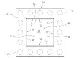
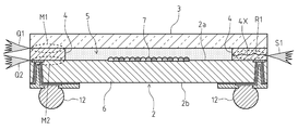
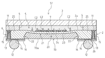
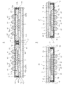
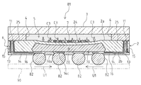
- FIG. 1 is a cross-sectional view illustrating a configuration of a solid-state imaging device according to a first embodiment of the present technology. It is a figure showing the back side of the semiconductor substrate concerning a 1st embodiment of this art.
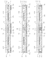
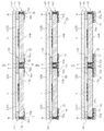
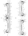
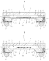
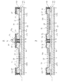
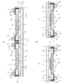
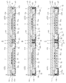
- FIG. 4 is an explanatory diagram illustrating a method for manufacturing the solid-state imaging device according to the first embodiment of the present technology.
- FIG. 4 is an explanatory diagram illustrating a method for manufacturing the solid-state imaging device according to the first embodiment of the present technology.
- FIG. 4 is an explanatory diagram illustrating a method for manufacturing the solid-state imaging device according to the first embodiment of the present technology.
- FIG. 4 is an explanatory diagram illustrating a method for manufacturing the solid-state imaging device according to the first embodiment of the present technology.
- FIG. 4 is an explanatory diagram illustrating a method for manufacturing the solid-state imaging device according to the first embodiment of the present technology.
- FIG. 4 is an explanatory diagram illustrating a method for manufacturing the solid-state imaging device according to the first embodiment of the present technology.
- FIG. 3 is an explanatory diagram illustrating a concave portion of the solid-state imaging device according to the first embodiment of the present technology.
- FIG. 14 is a diagram illustrating a configuration of a solid-state imaging device of a comparative example for the present technology.
- FIG. 5 is an explanatory diagram illustrating an operation of the solid-state imaging device according to the first embodiment of the present technology. It is a sectional view showing the composition of the modification of the solid-state imaging device concerning a 1st embodiment of this art. It is a sectional view showing the composition of the solid-state imaging device concerning a 2nd embodiment of this art.
- FIG. 11 is an explanatory diagram illustrating a method for manufacturing the solid-state imaging device according to the second embodiment of the present technology.
- FIG. 11 is an explanatory diagram illustrating a method for manufacturing the solid-state imaging device according to the second embodiment of the present technology. It is an explanatory view about an operation of a solid-state imaging device according to a second embodiment of the present technology.
- FIG. 13 is an explanatory diagram illustrating a modification of the method of manufacturing the solid-state imaging device according to the second embodiment of the present technology.
- FIG. 13 is an explanatory diagram illustrating a modification of the method of manufacturing the solid-state imaging device according to the second embodiment of the present technology.
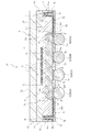
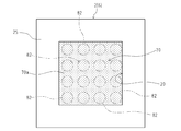
- FIG. 13 is an explanatory diagram illustrating a modification of the method of manufacturing the solid-state imaging device according to the second embodiment of the present technology. It is a sectional view showing the composition of the solid-state imaging device concerning a 3rd embodiment of this art. It is a figure showing the back side of the semiconductor substrate concerning a 3rd embodiment of this art.
- FIG. 14 is an explanatory diagram illustrating a method for manufacturing the solid-state imaging device according to the third embodiment of the present technology.
- FIG. 14 is an explanatory diagram illustrating a method for manufacturing the solid-state imaging device according to the third embodiment of the present technology. It is an explanatory view about an operation of a solid-state imaging device according to a third embodiment of the present technology.
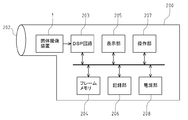
- 1 is a block diagram illustrating a configuration example of an electronic device including a solid-state imaging device according to an embodiment of the present technology.
- the shape of a semiconductor substrate forming the solid-state imaging device is devised.
- the purpose of the present invention is to prevent damage due to an increase in pressure in the cavity.
- a solid-state imaging device 1 includes an image sensor 2 as a solid-state imaging device, a glass 3 as a translucent lid member, and a support as a support for supporting the glass 3 on the image sensor 2. And a partition 4.
- the solid-state imaging device 1 has a package structure in which the glass 3 is mounted on the image sensor 2 via the partition 4 and the cavity 5 is provided between the image sensor 2 and the glass 3.
- the glass 3 is supported by the partition 4 provided on the surface 2 a, which is the light receiving side of the image sensor 2, so as to face the surface 2 a with respect to the image sensor 2.
- the partition 4 seals the periphery between the image sensor 2 and the glass 3, and forms a cavity 5 between the image sensor 2 and the glass 3.
- the solid-state imaging device 1 according to the present embodiment employs a so-called WCSP structure as a package structure.
- the image sensor 2 includes a silicon semiconductor substrate 6 made of silicon (Si), which is an example of a semiconductor.
- the surface 2a side (upper side in FIG. 1), which is one plate surface of the semiconductor substrate 6, is defined as a light receiving side. I do.
- the image sensor 2 is a rectangular plate-shaped chip having a plurality of light receiving elements formed on the front surface 2 a side, and the glass 3 is disposed via a partition 4 provided on the light receiving side of the semiconductor substrate 6.
- the image sensor 2 according to the present embodiment is a CMOS image sensor. However, the image sensor 2 may be a CCD type image sensor.
- the image sensor 2 is constituted by the semiconductor substrate 6.
- an image sensor element is formed on the front side of the semiconductor substrate 6. That is, the image sensor 2 has, on the front surface 2a side, a pixel area 8 as a light receiving section, which is a light receiving area including a plurality of pixels 7 formed in a predetermined arrangement such as a Bayer arrangement.
- the area around 8 is a peripheral area.
- the pixel region 8 includes an effective pixel region for generating, amplifying, and reading out signal charges by photoelectric conversion in each pixel 7.
- the pixel 7 includes a photodiode serving as a photoelectric conversion unit having a photoelectric conversion function, and a plurality of pixel transistors.
- the photodiode has a light receiving surface that receives light incident from the surface 2a side of the image sensor 2, and generates an amount of signal charge according to the amount (intensity) of light incident on the light receiving surface.
- the plurality of pixel transistors include, for example, MOS transistors that respectively perform amplification, transfer, selection, and reset of signal charges generated by the photodiode. Note that the plurality of pixels 7 may have a shared pixel structure in which the photodiodes and transfer transistors forming the plurality of unit pixels share another pixel transistor.
- a color filter and an on-chip lens are formed on each pixel via an anti-reflection film made of an oxide film or the like or a flattening film made of an organic material with respect to the semiconductor substrate 6. 7 are formed. Light incident on the on-chip lens is received by a photodiode via a color filter, a flattening film, and the like.
- the image sensor 2 according to the present technology is not limited to those having these structures.
- the glass 3 is provided on the light receiving side of the image sensor 2 at a predetermined distance from the image sensor 2.
- the glass 3 is an example of a lid member, and is a rectangular plate-shaped member having substantially the same size as the image sensor 2.
- the glass 3 is provided so as to substantially match the outer shape of the image sensor 2 in a plan view and in parallel with the image sensor 2.
- the glass 3 has a lower surface 3b, which is a plate surface facing the image sensor 2, and an upper surface 3a, which is the opposite surface. Light transmitted through the glass 3 is incident on the light receiving surface of the image sensor 2.
- the glass 3 generally transmits various light incident from an optical system such as a lens located above the glass 3 and transmits the light to the light receiving surface of the image sensor 2 facing the glass 3 via the cavity 5.
- the glass 3 has a function of protecting the light receiving surface side of the image sensor 2 and a function of blocking the intrusion of moisture (water vapor) and dust from the outside into the cavity 5 together with the partition wall 4.
- the lid member according to the present technology besides a glass plate, for example, a plastic plate or a silicon plate that transmits only infrared light can be used.
- the glass 3 has a surface on which a filter film for various wavelengths is formed, and at the same time, an antireflection for preventing reflection from inside and outside of the cavity 5.
- the membrane may be coated.
- the partition 4 is provided on the light receiving side of the image sensor 2, supports the glass 3 with respect to the image sensor 2, and forms a cavity 5 between the image sensor 2 and the glass 3.
- the partition 4 is provided in a peripheral region excluding the pixel region 8 so as to surround the pixel region 8 on the surface 2 a of the image sensor 2.
- the partition wall 4 is interposed between the front surface 2a of the image sensor 2 and the lower surface 3b of the glass 3, and functions as a sealing portion that closes between the image sensor 2 and the glass 3. That is, the partition wall 4 blocks the intrusion of moisture and dust from the outside into the cavity 5 together with the glass 3.
- the partition wall 4 is formed over the entire circumference along the outer shape of the glass 3, and is provided so as to form a rectangular frame shape in plan view.
- the partition wall 4 is provided at a position within the outer shape of the glass 3 so as to be along the outer edge of the glass 3 in plan view.
- the partition 4 is provided so that its outer surface 4c is substantially flush with the outer surface 3c of the glass 3.
- the material of the partition 4 is, for example, a photosensitive adhesive such as a UV (ultraviolet) curable resin which is an acrylic resin, a thermosetting resin such as an epoxy resin, or a mixture thereof.
- the partition wall 4 is formed on the surface 2a of the image sensor 2 by application using a dispenser, patterning using a photolithography technique, or the like.
- a photosensitive resin that can freely form a pattern by photolithography is generally suitably used.
- the partition wall 4 When the partition wall 4 is made of a resin material, the partition wall 4 functions as an adhesive for bonding the image sensor 2 and the glass 3 while being separated from each other.
- the partition walls 4 are not limited to those made of resin, and are provided by attaching a structure made of an inorganic material such as ceramics such as glass or metal or silicon to the image sensor 2 and the glass 3 with an adhesive or the like. It may be a configuration. By forming the partition walls 4 from a structure made of glass or the like, an effect of preventing moisture permeation can be expected.
- the cavity 5 is a flat rectangular space between the image sensor 2 and the glass 3. Specifically, the cavity 5 is formed by the surface 2 a of the image sensor 2, the lower surface 3 b of the glass 3, and the inner side surface 4 a of the partition 4. The inside of the cavity 5 is a space portion on the image sensor 2 that is completely isolated and protected from the outside.
- the light incident on the glass 3 from the outside changes its incident angle once due to the influence of the refractive index of the material of the glass 3, but since the inside of the cavity 5 is an air layer having a refractive index of 1, the on-chip formed in the pixel 7 As for the incident light to the lens, the original incident angle of the incident light to the glass 3 is reproduced.
- a plurality of electrode pads 11 are formed on the surface 2a side of the image sensor 2 as terminals for transmitting and receiving signals to and from the outside.
- a material of the electrode pad 11 for example, an aluminum material or the like is used.
- a group of solder balls 12 as a solder portion for mounting the image sensor 2 is provided on the other surface (the surface opposite to the surface 2 a) of the semiconductor substrate 6 on the back surface 2 b side.
- the electrode pads 11 are electrically connected to the solder balls 12.
- the image sensor 2 is mounted on a substrate such as an interposer substrate in a product, for example.
- the electrode pad 11 is formed on the surface 2 a of the image sensor 2 at a position directly below the partition 4.
- the electrode pad 11 is connected to the solder ball 12 via a wiring layer 14 extended to be embedded in a through via (TSV: Through Silicon Silicon Via) 13 formed from the back surface 2 b side of the image sensor 2. I have.
- TSV Through Silicon Silicon Via
- the through via 13 is formed by burying an in-hole wiring portion 14 a forming a wiring layer 14 via an insulating film 15 on the inner surface of a hole formed to penetrate the semiconductor substrate 6.
- the in-hole wiring portion 14a forms a wiring layer 14 together with the planar wiring portion 14b formed on the back surface 2b side of the semiconductor substrate 6, and the planar wiring portion 14b is connected to the solder ball 12.
- DRIE Deep Reactive Ion Etching
- connection configuration of the electrode pad 11 may be, for example, a configuration in which the electrode pad 11 is connected to the solder ball 12 from the front surface 2a side of the image sensor 2 via a bonding wire.
- the electrode pad 11 is formed outside the partition wall 4 on the surface 2a side of the image sensor 2, for example.
- the wiring layer 14 is formed of, for example, a low-resistance metal material such as copper (Cu) having a low resistance and advantageous for transmitting a high-speed signal.
- the wiring layer 14 can be formed of tungsten (W), titanium (Ti), tantalum (Ta), titanium-tungsten alloy (TiW), polysilicon, or the like, in addition to copper (Cu).
- the formation portion of the wiring layer 14 in the image sensor 2 is formed by an insulating film 15 made of an oxide film, a nitride film, or the like formed under the wiring layer 14 so that the wiring layer 14 does not directly contact the semiconductor substrate 6. Covered. That is, the insulating film 15 is interposed between the wiring layer 14 and the semiconductor substrate 6.
- a solder resist made of an insulating resin is provided on the back surface 2b side of the image sensor 2 so as to cover the entire back surface 2b while having an opening 16a for opening only a connection portion of the solder ball 12 to the wiring layer 14.
- (Solder mask) 16 is formed.
- the solder resist 16 is also buried in the through via 13 and is formed so as to cover the in-hole wiring portion 14a and the planar wiring portion 14b of the wiring layer 14.
- the solder resist 16 has a function of defining a contact area between the wiring layer 14 and the solder ball 12 and preventing a short circuit between the adjacent solder balls 12.
- a wiring layer 14 is laid inside the solder resist 16. Thereby, the space between the wirings is reliably covered, and short-circuiting between the wirings due to, for example, conductive foreign matter is prevented.
- the plurality of solder balls 12 function as external terminals, and are arranged in an appropriate arrangement according to the number of signals of the image sensor 2 and the product substrate.
- the solder balls 12 are arranged on the back surface 2b side of the image sensor 2 along the outer shape of the rectangular chip of the image sensor 2 (see FIG. 2).
- the process for providing the solder balls 12 includes a process of placing the solder balls 12 of uniform size in a state where the flux is applied to the openings 16a of the solder resist 16 with high positional accuracy, or a process of printing the solder resist 16 using a printing technique. A process of printing solder paste in the opening 16a of the above and then reflowing the solder paste to form solder into a ball shape is employed.
- the solid-state imaging device 1 adopting the WCSP structure has a configuration in which electrodes are formed by the through vias 13 penetrating the front surface 2a and the back surface 2b of the image sensor 2, thereby eliminating wiring by wire bonding. That is, in the solid-state imaging device 1, the wiring layer 14 extending from the electrode pad 11, which is the signal connection end of the image sensor 2, through the through via 13 penetrating the front surface 2 a and the back surface 2 b of the image sensor 2, It is connected to a ball 12.
- a connection area for wire bonding is not required. Therefore, miniaturization and cost reduction can be achieved. Further, according to the WCSP structure, since it is possible to assemble using a so-called wafer process in a cream room, dust reduction can be expected, and it is possible to contribute to an improvement in the performance of the image sensor 2.
- the thickness of the image sensor 2 is 300 to 600 ⁇ m.
- the thickness of the glass 3 is 100 to 500 ⁇ m.
- the thickness (height) dimension of the partition wall 4 is 10 to 50 ⁇ m.
- the thickness of the solder resist 16 is 10 to 30 ⁇ m. Note that these dimensions are merely examples, and appropriate dimensions are adopted as the dimensions of each unit according to the device structure, pixel size, and the like of the solid-state imaging device 1.
- the solid-state imaging device 1 undergoes reflow for melting the solder balls 12 for bonding, for example, when mounted on a product substrate.
- the solid-state imaging device 1 is exposed to a temperature atmosphere of, for example, about 250 ° C.
- the gas containing moisture (steam) in the cavity 5 is heated, and the internal pressure (steam pressure) of the cavity 5 increases.
- the partition wall 4 that supports the glass 3 on the image sensor 2 is made of resin, moisture transmitted through the partition wall 4 exists in the cavity.
- the increase in the internal pressure of the cavity 5 causes damage such as cracks in the components of the solid-state imaging device 1 such as the semiconductor substrate 6, the glass 3, and the partition walls 4 that support the image sensor 2, and separation between the members. It can be a cause.
- damage occurs, moisture, dust, and the like enter the cavity 5 from the damaged portion, and the performance of the device is reduced. Therefore, the solid-state imaging device 1 according to the present embodiment has the following configuration.
- the semiconductor substrate 6 has a concave portion 20 formed on the back surface 2 b side to partially reduce the thickness of the semiconductor substrate 6.
- the concave portion 20 is a depressed portion formed in the image sensor 2 which is a rectangular plate-shaped chip so as to open toward the back surface 2b.
- the concave portion 20 has a bottom surface portion 21 substantially parallel to the plate surface of the semiconductor substrate 6 and a side surface portion 22 forming an inner surface of the concave portion 20.
- the bottom surface portion 21 is a portion that forms a bottom surface 23 which is a surface opposite to the front surface 2a in the image sensor 2 and is a horizontal surface.
- the side surface portion 22 is a surface portion formed between the bottom surface portion 21 and the back surface 2b.
- the concave portion 20 has a shape along the outer shape of the image sensor 2 as a bottom view shape. Therefore, the concave portion 20 is a rectangular concave portion formed to have a rectangular shape or a square shape when viewed from the bottom of the image sensor 2 (see FIG. 2). For this reason, in the concave portion 20, the bottom surface portion 21 is formed in a rectangular shape along the outer shape of the image sensor 2, and the side surface portion 22 is formed along four sides of the bottom surface portion 21.
- the semiconductor substrate 6 having such a recess 20 has a frame-like shape with the back surface 2b side being an opening side.
- the range of the region where the concave portion 20 is formed is, for example, a range including the pixel region 8.
- the recess 20 is formed, for example, so as to be included in the formation range of the cavity 5, in other words, the range inside the partition 4.
- the portion of the image sensor 2 where the concave portion 20 is formed except for the peripheral edge portion is thinned to be a diaphragm-shaped portion.
- the image sensor 2 is formed in the semiconductor substrate 6 in a frame shape so as to surround a thin plate portion 24 formed in a rectangular shape corresponding to a formation range of the concave portion 20 and an outer periphery of the thin plate portion 24. It has a thick plate portion 25 whose thickness is increased on the back surface 2b side with respect to the thin plate portion 24.
- the thick plate portion 25 has linear portions along each of the four sides of the rectangular shape corresponding to the formation range of the concave portion 20, and these linear portions form a rectangular frame shape in a bottom view.
- the thickness of the thin plate portion 24 formed by the concave portion 20 is, for example, about 1 / to ⁇ of the plate thickness of the thick plate portion 25 which is the thickness portion of the normal semiconductor substrate 6.
- the lower surface of the thick plate portion 25, which is a portion around the concave portion 20, is the rear surface 2 b of the image sensor 2.
- the recess 20 is basically formed by etching.
- the method for forming the concave portion 20 is not limited to etching, but may be any method that can partially remove the semiconductor substrate 6. The method for forming the recess 20 will be described later.
- the side surface portion 22 forming the concave portion 20 will be described.
- the side surface portion 22 has a first inclined surface 31 inclined in a predetermined direction with respect to the plate surface of the semiconductor substrate 6, and a bent shape in a sectional view of the semiconductor substrate 6 together with the first inclined surface 31. And a second inclined surface 32.
- the first inclined surface 31 is a surface that forms a portion on the back surface 2 b side (hereinafter, also referred to as a “lower side”) of the side surface portion 22, and the second inclined surface 32 is
- the side surface portion 22 is a surface forming the surface 2a side (hereinafter, also referred to as “upper side”).
- the side surface portion 22 has the first inclined surface 31 and the second inclined surface 32, and a substantially horizontal “V” in which the outside (the left and right outside in FIG. 1) of the recess 20 is a convex side in a cross-sectional view of the solid-state imaging device 1. Form a curved surface to form a letter.
- the first inclined surface 31 is inclined from the inside to the outside in the left-right direction from the lower side to the upper side with respect to the direction perpendicular to the plate surface of the semiconductor substrate 6 (vertical direction in FIG. 1)
- the second inclined surface 32 is inclined from the lower side to the upper side toward the inside from the outside in the left-right direction with respect to the vertical direction.
- the upper end of the second inclined surface 32 is connected to the bottom surface 23 so as to form an obtuse angle with the bottom surface 23 of the bottom surface portion 21.
- the first inclined surface 31 and the second inclined surface 32 correspond to the plate surface of the semiconductor substrate 6, respectively.
- the area size A1 of the first inclined surface 31 is smaller than the area size A2 of the second inclined surface 32.
- the size relationship (the size relationship between the size A1 and the size A2) of the size of the formation region of the first slope 31 and the second slope 32 in the depth direction of the recess 20 is not particularly limited.
- the side surface portion 22 of the concave portion 20 includes a (111) plane of the crystal of the semiconductor substrate 6 or a plane equivalent thereto (hereinafter collectively referred to as a “ ⁇ 111 ⁇ plane”).
- the semiconductor substrate 6 is a silicon substrate, and the ⁇ 111 ⁇ plane is based on the crystal structure of silicon, and is a crystal plane formed by anisotropic etching on the silicon substrate.
- the first inclined surface 31 and the second inclined surface 32 forming the side surface portion 22 of the recess 20 are both ⁇ 111 ⁇ surfaces. That is, the first inclined surface 31 and the second inclined surface 32 are both silicon crystal surfaces formed by anisotropic etching.
- the angle ⁇ 1 and the angle ⁇ 2 with respect to the horizontal direction O1 are both about 55 ° (54 °). .7 °), which are substantially the same angle.
- Anisotropic etching is a type of wet etching, and is a technique generally used in the manufacturing process of MEMS (Micro Electro Mechanical Systems).
- MEMS Micro Electro Mechanical Systems
- a desired opening pattern is formed on a processed surface of a semiconductor substrate such as a silicon substrate with an oxide film, a nitride film, an alkali-resistant resist, or the like, and the pattern is used as a mask to form a strong alkali such as KOH (potassium hydroxide).
- KOH potassium hydroxide
- the etching is performed by dipping in an aqueous solution. According to the anisotropic etching, the opening shape is uniquely determined in such a manner that the ⁇ 111 ⁇ plane is exposed depending on the crystal orientation of the semiconductor substrate.
- a single crystal silicon substrate having a surface orientation of (100) is often used as a semiconductor constituting an image sensor.
- the solid-state imaging device 1 is configured as a WCSP structure having the following configuration. That is, the solid-state imaging device 1 is formed on the semiconductor substrate 6 in which the concave portion 20 is formed on the back surface side and the image sensor element is formed on the front surface side, and is formed on the flat portion outside the concave portion 20 of the semiconductor substrate 6.
- a wiring layer 14 connected and extended, a solder ball 12 formed on the wiring layer 14 via a land (not shown), and an image sensor element formed to surround the image sensor element of the semiconductor substrate 6 are formed. It has a partition wall 4 for isolating a space on the site as a cavity 5 from the outside, and a glass 3 bonded on the partition wall 4.
- a silicon wafer 40 on which the pixels 7 are formed is prepared.
- the silicon wafer 40 has been subjected to various processes for forming the image sensor 2. That is, the silicon wafer 40 is a semiconductor wafer in which a plurality of portions to be the image sensor 2 in which the group of pixels 7 is formed on one plate surface side are formed in a predetermined arrangement. In recent years, an 8 inch or 12 inch wafer is mainly used as the silicon wafer 40.
- the formation of the wall portion 44 serving as the partition wall 4 and the attachment of the glass plate 43 serving as the glass 3 are performed on the silicon wafer 40.
- the glass plate 43 may be attached.
- the wall portion 44 may be formed on the glass plate 43 side in advance. You may paste on 40a.
- the glass plate 43 is an example of a plate material having a light transmitting property.
- the wall portion 44 is formed along a predetermined arrangement of the plurality of image sensors 2 so as to surround the group of pixels 7. That is, the wall portion 44 is formed in a lattice shape in a plan view corresponding to the rectangular region that will eventually become the solid-state imaging device 1.
- the wall portion 44 As a method of forming the wall portion 44, for example, patterning using photolithography technology, screen printing, etching, coating with a dispenser, and the like are used. By bonding the silicon wafer 40 and the glass plate 43 via the wall portion 44, a cavity 45 to be the cavity 5 in each solid-state imaging device 1 is formed.
- the partition walls 4 are formed of a structure such as glass or metal
- the structures formed in a lattice shape are attached to the silicon wafer 40 and the glass plate 43 with a predetermined adhesive.
- the structure attaching step is preferably performed in a clean room with high cleanliness so that dust does not enter the cavity 45.
- a step of providing a glass plate 43 at a predetermined distance from the silicon wafer 40 via 44 is performed.
- a protective sheet is formed on the surface 43a of the glass plate 43. 50 is pasted.
- the protection sheet 50 is for protecting the front surface 43a of the glass plate 43 from handling in the step of shaving the silicon wafer 40 from the back surface 40b side.
- a BG (Back-Grinding) step of cutting the silicon wafer 40 from the back surface 40b side in order to make the silicon wafer 40 a desired thickness that does not affect the device characteristics is performed. Be done.
- the protection sheet 50 protects the surface 43a of the glass plate 43 from handling.
- a back grinding wheel 58 such as a diamond wheel is used, and the silicon wafer 40 is polished. According to the BG process, the thickness of the silicon wafer 40 becomes the desired thickness T2 smaller than the original thickness T1.
- the protective sheet 50 is attached to the entire surface 43a of the glass plate 43 by using equipment such as a laminator device.
- equipment such as a laminator device.
- the protective sheet 50 for example, a type in which the adhesive force is reduced by irradiating UV light or a type in which the adhesive force is reduced by heating is used.
- a mirror finishing process such as chemical polishing or dry polishing may be performed after the BG process.
- a step of forming a first insulating film 52 such as a nitride film such as Si 3 N 4 or an oxide film such as SiO 2 on the back surface 40b of the silicon wafer 40 is performed.
- a first insulating film 52 such as a nitride film such as Si 3 N 4 or an oxide film such as SiO 2
- PECVD Plasma-Enhanced Chemical Vapor Deposition
- High-frequency sputtering or other film-forming methods may be used.
- the protective sheet 50 used in the previous process is formed in a state where the protective sheet 50 is attached as it is to protect it from scratches during handling and various reaction gas atmospheres during the PECVD process. Or may be reattached to another protective sheet. Further, if there is no fear of damage to the glass plate 43 during handling or contamination of the glass plate 43 during PECVD, the film can be formed without the protective sheet 50.
- the first insulating film 52 is patterned into a desired pattern, and a photolithography process (photolithography process) for exposing the underlying silicon wafer 40 is performed.
- a fine pattern opening for opening a through hole 40c (see FIG. 4B) for the through via 13 formed through the electrode pad 11 from the back surface 40b side of the silicon wafer 40.
- the first insulating film 52 is partially formed by a technique such as reactive ion etching (RIE) so that an opening 52b for forming the recess 20 by thinning the silicon wafer 40 is formed. Is removed.
- RIE reactive ion etching
- patterning is performed using a photoresist 53 made of a predetermined photosensitive material. After the first insulating film 52 is partially removed by RIE or the like, the photoresist 53 is removed. You. Specifically, the following steps are sequentially performed as a patterning step. That is, application and drying of a photoresist 53 as a mask ⁇ exposure of the mask and patterning ⁇ removal of the mask corresponding to the openings 52a and 52b with a developer ⁇ removal of the residue remaining in the removed portion with argon or oxygen if necessary. , Etching of the mask opening by RIE ⁇ removal of the unnecessary photoresist 53 ⁇ plasma cleaning of the residue remaining in the removed portion with argon or oxygen if necessary.
- a step of forming a through hole 40c for the through via 13 is performed.
- a photoresist 54 is formed by patterning using a photolithography technique so that a portion corresponding to the opening 52a is opened in the first insulating film 52 formed in the previous step. That is, the photoresist 54 has an opening 54a continuous with the opening 52a of the first insulating film 52.
- through holes 40c are formed in the silicon wafer 40 through the openings 52a of the first insulating film 52 and the openings 54a of the photoresist 54 by etching.
- the step of forming the through hole 40c is a step of forming a through hole having a so-called high aspect ratio
- the formation of the through hole 40c is performed, for example, by an etching process having higher directivity than normal RIE. Is used. In DRIE, high-density plasma is used for normal RIE, and therefore, photoresist 54 having relatively high plasma resistance is used as photoresist 54.
- the photoresist 54 is removed.
- a second insulating film 55 is formed so as to cover the entire surface including the inner surface of the through hole 40c (FIG. 4C).
- the second insulating film 55 By forming the second insulating film 55 over the entire surface, the inner surface of the through hole 40c and the portion of the opening 52b of the first insulating film 52 become a single-layer insulating film portion of the second insulating film 55.
- the portion where the first insulating film 52 exists has a two-layer structure of an insulating film including the first insulating film 52 and the second insulating film 55, so that high insulating properties can be obtained.
- the insulating film structure including the one-layer portion formed by the second insulating film 55 and the two-layer portion formed by the first insulating film 52 and the second insulating film 55 becomes the insulating film 15 in the solid-state imaging device 1.
- FIG. 4C the illustration of the first insulating film 52 is omitted.
- the second insulating film 55 is formed so as to cover the contact portion on the back surface of the electrode pad 11 facing the upper side of the through hole 40c and the portion where the recess 20 is formed in the silicon wafer 40. Therefore, as shown in FIG. 4C, the portion of the contact portion on the back surface of the electrode pad 11 and the portion where the concave portion 20 is formed in the second insulating film 55 are removed by patterning using a photolithography technique. As a result, in the second insulating film 55, a contact hole 55a for exposing the back surface of the electrode pad 11 and an opening 55b for forming the concave portion 20 are formed.
- a resist is coated on the second insulating film 55 including the inside of the through hole 40c by coating or the like.
- the viscosity of the resist and the coating method it is necessary to adjust the viscosity of the resist and the coating method so that the resist does not enter only into the deep through hole 40c.
- an exposure apparatus that can provide a wide depth of focus or a unit that performs exposure of the bottom of the through hole 40c and exposure of the other portion in two steps is appropriately used.
- a copper wiring layer 56 to be the wiring layer 14 in the solid-state imaging device 1 is formed on the back surface 40 b side of the silicon wafer 40.
- the copper wiring layer 56 is for forming the solder balls 12 on the back surface 40b side of the silicon wafer 40 in the WCSP structure.
- the copper wiring layer 56 extends from the back surface of the electrode pad 11 through the inside of the through hole 40c, and the solder ball 12 is connected to the extending portion.
- the copper wiring layer 56 includes a wiring portion 56a in the hole that becomes the wiring portion 14a in the hole (see FIG. 1), and a planar wiring portion 56b that is formed along the back surface 40b and becomes the wiring portion 14b (see FIG. 1). Having.
- a seed layer which is a thin film of, for example, titanium (Ti) or copper (Cu) is formed in advance by a film forming method such as sputtering.
- the seed layer becomes an electrode when the copper wiring layer 56 is embedded in the through hole 40c by the electroplating method.
- a barrier metal film for preventing diffusion of the wiring portion 56a in the hole may be formed by sputtering or the like, for example, with tantalum (Ta) or titanium (Ti). .
- a resist pattern corresponding to the wiring pattern is patterned by a photolithography process, and then, by an electroplating method using the seed layer as an electrode, a copper wiring is formed in a portion where the seed layer is exposed by patterning.
- Layer 56 is formed. As a result, an in-hole wiring portion 56a and a planar wiring portion 56b that form the through via 13 are formed.
- the copper wiring layer 56 is generally formed with a thickness of about 10 ⁇ m, but the thickness of the copper wiring layer 56 is appropriately increased or decreased according to the type and number of signals of the solid-state imaging device 1.
- the unnecessary resist pattern is removed by using a dedicated stripping solution or a rinsing solution, and the seed layer is removed by wet etching or the like.
- a step of forming a solder resist 57 is performed.
- the solder resist 57 is formed to prevent a short circuit between wirings of the copper wiring layer 56 and to define a position where the solder ball 12 is mounted.
- a land opening 57a for exposing the copper wiring layer 56 is formed in a portion where the solder ball 12 is to be mounted, according to the size of the solder ball 12.
- solder resist 57 for example, a photosensitive resin using an epoxy resin or the like as a base resin is used.
- the land openings 57a can be freely designed by using a photomask used in the photolithography process.
- the following processes are sequentially performed. That is, application and drying of the solder resist 57 ⁇ patterning by exposing the mask corresponding to the land opening 57 a ⁇ removal of the solder resist 57 in the portion of the land opening 57 a with a developing solution ⁇ removal of the residue remaining in the removed portion with argon or This is a process such as plasma cleaning with oxygen.
- the formation pattern of the solder resist 57 is such that the solder resist 57 does not interfere with the mounting portion of the solder ball 12 and the formation portion of the concave portion 20.
- the solder resist 57 is embedded in the through hole 40c in which the in-hole wiring portion 56a is formed.
- a step of forming a recess 20 for partially reducing the thickness of the silicon wafer 40 corresponding to each image sensor 2 is performed on the back surface 40b side, which is the other plate surface of the silicon wafer 40. That is, by partially removing the silicon wafer 40 from the back surface 40b side at the portion corresponding to each image sensor 2, the concave portion 20 corresponding to each solid-state imaging device 1 is formed.
- the step of forming the recess 20 includes a first etching step and a second etching step, and the recess 20 is formed by a two-stage etching step.
- the step of forming the concave portion 20 will be described in detail.
- the photoresist 61 is formed by the photolithography process as described above. That is, after the photoresist 61 is applied and dried, patterning is performed by exposure, and a rectangular or square opening 61a corresponding to the portion where the concave portion 20 is formed is removed with a developing solution. The remaining residue is cleaned.
- the photoresist 61 covers the solder resist 57 and also covers the planar wiring portion 56b of the copper wiring layer 56 exposed from the land opening 57a.
- the photoresist 61 may be the same as the photoresists 53 and 54 described above, or may be a different type of resist having different viscosity and physical properties from those of the photoresists. However, since a strong alkaline solution is used in forming the concave portion 20 as described later, it is preferable that the photoresist 61 has strong alkali resistance.
- a first etching step of forming a half recess 20X by removing a portion corresponding to the recess 20 of the silicon wafer 40 by dry etching is performed.
- the silicon portion exposed from the opening 61a of the photoresist 61 on the back surface 40b side of the silicon wafer 40 is etched to a required depth by RIE which is a kind of dry etching. You. Thereby, the semi-recess 20X is formed.
- the semi-recess 20X has a rectangular or square shape when viewed from the bottom.
- the semi-recess 20X has, as an etching surface, a bottom surface 20Xa substantially parallel to the surface 40a and a side surface 20Xb substantially perpendicular to the bottom surface 20Xa. That is, the semi-recess 20X has a flat concave shape that is substantially rectangular in a side cross-sectional view by the bottom surface 20Xa and the surrounding side surface 20Xb, and that is rectangular in plan.
- the first etching process is a hole processing in a depth direction (longitudinal direction) perpendicular to the plate surface of the silicon wafer 40.
- the depth of the semi-recess 20 ⁇ / b> X affects the bent shape having a substantially horizontal “V” cross section of the side surface 22 of the final recess 20. For this reason, the depth of the semi-recess 20 ⁇ / b> X is determined according to a desired shape of the side surface 22 of the recess 20.
- a second etching step of forming the recess 20 by digging the half recess 20X by anisotropic etching is performed.
- the half-recess 20X formed by RIE is put into a strong alkaline aqueous solution such as KOH (potassium hydroxide) to perform anisotropic etching of silicon.
- a protective sheet 62 is attached by a dedicated facility to protect the surface 43a of the glass plate 43.
- anisotropic etching for example, a so-called batch-type wet etching apparatus for processing a plurality of silicon wafers 40 at once is used.
- the wafer is put into a KOH solution heated to about 60 to 80 ° C., and the wafer is rotated and rocked so that the etching is uniform within the plane of the wafer. Done.
- TMAH tetramethylammonium hydroxide
- EDP ethylenediamine / pyrocatechol
- the unnecessary photoresist 61 is removed as shown in FIG. 6C.
- the residue remaining on the removed portion of the photoresist 61 is cleaned by plasma cleaning or the like.
- the alkali solution may be washed by a method such as QDR (Quick Dump Rinse), and then moisture may be dried.
- the concave portion 20 is formed, the silicon wafer 40 is partially thinned from the back surface 40b side, and the diaphragm corresponding to each image sensor 2 is formed by the diaphragm by the concave portion 20. A shape is formed.
- a silicon substrate having a (100) plane orientation widely used in image sensors and LSI manufacture exposes a (111) plane having an angle of about 55 degrees with respect to a plane end face when anisotropic etching is performed. Etching of the (100) plane proceeds so as to cause the etching. For this reason, as the etching depth for forming the semi-recess 20X becomes deeper, the "-" shape (horizontal "V" shape) in cross-section formed in the (111) plane orientation becomes larger.
- the area size A1 of the first slope 31 and the area size A2 of the second slope 32 in the depth direction of the recess 20 in the side surface portion 22 of the recess 20 become larger. (See FIG. 1).
- FIGS. 8A and 8B when the depth of the concave portion 20 is constant at the depth D1, the etching depth (D2, D3) of the half concave portion 20X increases, and the side surface of the concave portion 20 increases.
- the area ratio of the first inclined surface 31 increases (the area ratio of the second inclined surface 32 decreases). That is, as the depth of the semi-recess 20X increases, the area dimension A1 of the first inclined surface 31 in the depth direction increases.
- a rectangular hatched portion B1 surrounded by a two-dot chain line indicates a region to be removed in order to form the semi-recess 20X in the silicon wafer 40.
- the depth of the semi-recess 20X is a relatively shallow depth D2, as shown in FIG. 8B, whereas the depth of the semi-recess 20X is a relatively shallow depth D3.
- the width of the recess 20 in the lateral direction is increased.
- the lateral width when the depth of the semi-recess 20X is a deep depth D3 is smaller than the lateral expansion dimension W2 when the depth of the semi-recess 20X is a shallow depth D2.
- the dimension W3 in the direction becomes larger.
- the lateral spread dimension (W2, W3) is determined by the position P1 of the left and right ends of the semi-recess 20X in the direction along the plate surface (the left-right direction in FIGS. 8A and 8B) in a cross-sectional view of the silicon wafer 40. And the position P2 of the vertex of the corner formed by the first inclined surface 31 and the second inclined surface 32 in the side surface portion 22 of the concave portion 20.
- the side surface 22 of the final recess 20 is determined by the etching depth of the half recess 20 X formed in advance in the first etching step.
- the bent shape of the first inclined surface 31 and the second inclined surface 32 can be controlled. Accordingly, for example, as shown in FIG. 8B, when it is desired to make the bent shape of the side surface portion 22 relatively large in the concave portion 20, the half concave portion 20X may be formed deeper in advance in the first etching step.
- the depth of the semi-recess 20X for example, there is a size of the thin plate portion 24 having a diaphragm structure required in the image sensor 2.
- the etching depth of the semi-recess 20X becomes deeper, the lateral spread in the anisotropic etching increases, and the area of the thin plate portion 24 becomes closer to the opening area of the lower end of the recess 20.
- the thin plate portion 24 there is a possibility that a stress difference may occur due to the deformation of the thin plate portion 24 in the pixel 7. Is preferably formed.
- solder balls 12 are formed below the solder resist 57 (upper side in FIG. 7A).
- the solder ball 12 is formed so as to be electrically connected to the planar wiring portion 56b of the copper wiring layer 56 via the land opening 57a of the solder resist 57.
- the flux is selectively transferred to the land openings 57a of the solder resist 57 by printing or the like, and the solder balls 12 formed in a desired size are mounted with high precision using dedicated mounting equipment.
- This is a method in which reflow is performed at about 250 to 260 ° C. to connect the solder balls 12 to the copper wiring layer 56 through the land openings 57a.
- the other is to selectively transfer the solder paste containing the flux to the land opening 57a by printing or the like, and then to perform reflow at about 250 to 260 ° C. to form the solder into a ball shape.
- the solder balls 12 are connected to the copper wiring layer 56 through the land openings 57a.
- the flux is appropriately cleaned after the solder balls 12 are formed.
- dicing is performed along a predetermined dicing line L1. That is, a step is performed in which the silicon wafer 40, the wall portion 44, and the glass plate 43 are cut and divided into individual portions corresponding to the image sensor 2 along a predetermined arrangement.
- the silicon wafer 40 forming the image sensor 2, the glass plate 43 forming the glass 3, the wall portion 44 forming the partition 4, and the like are separated.
- a plurality of chips (solid-state imaging device 1) generated by dicing are picked up from the protection sheet 62 by dedicated equipment or the like.
- FIG. 7B a package structure having image sensor 2, glass 3, and partition wall 4 having concave portion 20 formed on back surface 2b side, and having cavity 5 between image sensor 2 and glass 3 Are obtained.
- the concave portion 20 may be formed at a stage before the attachment. In this case, when performing anisotropic etching for forming the concave portion 20, it is necessary to protect the pixel surface with an alkali-resistant resist or film or the like so as not to affect the pixel surface of the silicon wafer 40. .
- the solid-state imaging device 1 and the method of manufacturing the same in the configuration including the package structure having the cavity 5 between the image sensor 2 and the glass 3, It is possible to prevent damages such as cracks of components and separation between members due to an increase in internal pressure.
- the operation and effect of the solid-state imaging device 1 and the method of manufacturing the same according to the present embodiment are specifically as follows.
- the back surface 2b of the image sensor 2 forms a plane parallel to the front surface 2a as a whole, and the image sensor 2 has a uniform plate thickness as a whole.
- the internal pressure of the cavity 5 increases due to the reflow for melting the solder ball 12, and as a result, stress is concentrated on a relatively weak portion in the package structure, which may cause damage.
- Relatively weak portions include a junction of the partition 4 with the image sensor 2 and the glass 3 and the partition 4 itself. There are the following modes for damage to the package structure.
- FIG. 9 there is a mode in which the partition wall 4 is peeled off at a joint portion of the partition wall 4 with the image sensor 2 or the glass 3 at a portion indicated by reference numerals M1 and M2. Since a resin material is often used as a material for the partition 4, the interface between the image sensor 2 and the partition 4 whose surface 2 a is an inorganic film such as SiN or SiO 2, or the glass 3 and the partition 4 Peels off at the interface of. When the partition wall 4 is peeled, the internal pressure of the cavity 5 is released from the peeled portion (see reference numerals Q1 and Q2).
- a crack 4X occurs in the partition wall 4, for example, in a portion indicated by a symbol R1 in FIG.
- the partition wall 4 is made of a resin material
- the material itself becomes brittle due to moisture absorption and high temperature, and the partition wall 4 itself is agglomerated and destroyed by a stress accompanying an increase in the internal pressure of the cavity 5.
- the damage mode may be a composite mode of the above-described peeling mode and a mode in which a crack occurs.
- Dry air is basically filled in the cavity 5 during the manufacturing process, but water vapor in the atmosphere before the glass plate 43 is covered or the wall 44 itself after the cavity 5 is formed (after sealing). Water vapor that passes through an adhesive for bonding the wall portion 44 to the silicon wafer 40 and the glass plate 43 is also mixed into the cavity 5 at the same time.
- the respective partial pressures increase with the temperature at the temperature during reflow (peak temperature T P : 240 to 260 ° C.) for mounting on a mother board or the like.
- the cavity pressure P P peak temperature T P may exceed the breakdown limit pressure P D package structure has.
- stress is concentrated on relatively weak portions in the package structure, and damage occurs.
- the dry air pressure PA0 is inversely proportional to the volume of the cavity 5 at each temperature (hereinafter, referred to as "cavity volume”)
- the cavity internal pressure PP becomes It will exceed the breaking limit pressure P D.
- the water vapor partial pressure P B0 also tends to sharply increase in accordance with the Tetens law, and accelerates the rise of the cavity internal pressure which is the sum of P A0 and P B0 .
- the solid-state imaging device 1 of the present embodiment since the image sensor 2 has the concave package 20 and the diaphragm-shaped package structure, when the internal pressure of the cavity rises, the semiconductor substrate 6 bends and the cavity volume increases. Can be increased. Thus, an excessive increase in the internal pressure of the cavity can be suppressed, and damages such as cracks in peripheral members of the cavity 5 and peeling between members during reflow can be prevented.
- the thin plate portion 24 formed by the concave portion 20 becomes a main deformed portion, and the thin plate portion 24 is elastically deformed in a curved shape so as to bulge outward (to the rear surface 2b side). That is, in the image sensor 2, the thin plate portion 24 mainly functions as a diaphragm (diaphragm) portion having a restoring force, and the portion bends outward with an increase in the cavity internal pressure.
- the cavity volume can be increased while following the rise in the internal pressure of the cavity generated during reflow. Thereby, an excessive increase in the cavity internal pressure can be suppressed, and damages such as cracks of constituent members of the solid-state imaging device 1 and separation between members can be prevented. As a result, performance degradation of the solid-state imaging device 1 can be prevented.
- the concave portion 20 is formed to have a rectangular shape when viewed from the bottom, and the image sensor 2 is configured to have a frame structure by the concave portion 20. According to such a configuration, it is possible to define a portion that bends and deforms with an increase in the cavity internal pressure as compared with a case where the entire silicon substrate is simply thinned, and to maintain strength as a structural body. In addition, it is possible to follow the original outer size of the image sensor 2, and it is possible to prevent an increase in the outer size of the package structure.
- the external terminals of the image sensor 2 are easily moved, and there is a concern that the external terminals may be structurally unstable.
- the external terminals may be structurally unstable.
- there is a problem that it is difficult to replace an existing structure. is there. Therefore, according to the structure in which the silicon substrate is partially thinned by the concave portions 20 as in the solid-state imaging device 1 according to the present embodiment, structural stability can be ensured, and the silicon substrate is originally formed. Since the thickness portion exists, it is possible to easily replace the existing structure.
- the thin plate portion 24 which is a main deformed portion in the image sensor 2 is a portion inside the peripheral portion where the solder balls 12 are provided. For this reason, it is possible to reduce the influence of the deformation of the image sensor 2 due to the increase of the cavity internal pressure on the connection portion of the solder ball 12 and the like. In this regard, for example, when the internal pressure of the cavity increases more than usual due to, for example, a large amount of moisture absorption into the cavity 5, it is advantageous because the bending deformation of the thin plate portion 24 can be largely allowed.
- the solid-state imaging device 1 According to the solid-state imaging device 1 according to the present embodiment, it is not necessary to provide a portion that communicates with the cavity 5 to prevent the internal pressure of the cavity from rising. For this reason, dust and the like can be prevented from entering the cavity 5 as much as possible, and characteristic deterioration due to dust and the like affecting the image quality can be eliminated.
- the solid-state imaging device 1 According to the solid-state imaging device 1 according to the present embodiment, it is not necessary to change the structure in the cavity 5 when preventing an increase in the cavity internal pressure. For this reason, for example, it is possible to avoid a malfunction or characteristic failure of the apparatus due to the detachment of another member in the cavity, which is a concern in a configuration in which another member such as a moisture absorbing member is provided in the cavity.
- the solid-state imaging device 1 is configured to satisfy the following conditions with respect to the cavity internal pressure. That is, the solid-state imaging device 1, the cavity pressure P P at predetermined peak temperature T P of reflow for melting the solder balls 12, the peeling between members forming a crack or a cavity 5 of the member forming the cavity 5 and it is configured to be lower than the resulting pressure, i.e. breaking limit pressure P D.
- the solid-state imaging device 1 In other words, in the solid-state imaging device 1, the following conditions are satisfied.
- that cavity internal pressure is cavity pressure P P peak temperature T P, bends and deforms the thin plate portion 24 formed by the recess 20, by its deformation, cavity volume increases.
- the cavity pressure P 2 when the cavity volume becomes V 2 is cavity pressure during the temperature T D to provide some damage to the cavity structure, that is smaller than the breakdown limit pressure P D (P 2 ⁇ P D Holds)
- the solid-state imaging device 1 is configured.
- the solid-state imaging device 1 is configured such that the action of reducing the internal cavity pressure is obtained by the bending of the semiconductor substrate 6 due to the recess 20.
- the concave portion 20 has the bottom surface portion 21 and the side surface portion 22, and the side surface portion 22 is formed by the first inclined surface 31 and the second inclined surface 32 in a sectional view.
- the concave portion 20 has the bottom surface portion 21 and the side surface portion 22, and the side surface portion 22 is formed by the first inclined surface 31 and the second inclined surface 32 in a sectional view.
- the side surface portion 22 of the concave portion 20 is formed by the ⁇ 111 ⁇ surface of the silicon substrate. That is, the first inclined surface 31 and the second inclined surface 32 forming the side surface portion 22 are both ⁇ 111 ⁇ surfaces. According to such a configuration, according to such a configuration, it is possible to stably deform the image sensor 2 when the internal pressure of the cavity increases while maintaining the strength of the image sensor 2.
- the concave portion 20 can be easily formed by anisotropic etching or the like utilizing the crystal structure of the semiconductor substrate 6.
- the concave portion 20 is formed by a first etching process using dry etching and a second etching process using anisotropic etching.
- a method of performing two-stage etching is employed. According to such a method, the etching time in each etching step, the temperature of the etching solution in anisotropic etching, and the method of holding and swinging the substrate in the etching apparatus are finely controlled, so that the etching depth can be improved. In other words, the thickness of the remaining portion of the semiconductor substrate 6 can be accurately formed. Further, as described above, by adjusting the depth of the semi-recess 20X formed by the first etching step, the bent shape by the first inclined surface 31 and the second inclined surface 32 on the side surface 22 of the concave 20 is formed. Can be controlled.
- Modified example of solid-state imaging device according to first embodiment> A modified example of the solid-state imaging device 1 will be described.
- the modified example described below is a modified example of the shape of the concave portion 20 in a sectional view.
- the recess 20 ⁇ / b> A has an opening shape along a rectangular shape in a side sectional view. That is, the concave portion 20 ⁇ / b> A of Modification 1 has an inner side surface 31 ⁇ / b> A that is a surface perpendicular to the bottom surface 23 of the bottom surface portion 21 as a surface forming the side surface portion 22. The upper end of the inner side surface 31A is connected to the bottom surface 23 so as to form a right-angled corner together with the bottom surface 23 of the bottom surface portion 21. As described above, the concave portion 20A of Modification 1 is formed by the rectangular bottom surface 23 and the inner side surfaces 31A formed on the four sides of the bottom surface 23.
- the concave portion 20A of the first modification is formed by, for example, dry etching such as RIE as in the above-described first etching step.
- the concave portion 20 ⁇ / b> B has an opening shape that follows a trapezoidal shape in a side sectional view. That is, the concave portion 20B of Modification Example 2 has, as a surface forming the side surface portion 22, an inclined surface 31B that is inclined from the lower side to the upper side and from the outside in the left-right direction to the inside in the vertical direction. The upper end of the inclined surface 31B is connected to the bottom surface 23 so as to form an obtuse angle with the bottom surface 23 of the bottom surface portion 21. As described above, the concave portion 20B of Modification 2 is formed by the rectangular bottom surface 23 and the inclined surfaces 31B formed on the four sides of the bottom surface 23. The concave portion 20B of Modification 2 is formed by anisotropic etching using the crystal structure of silicon, for example, as in the above-described second etching step.
- the configuration of the above modification can also prevent damages such as cracks of components and separation between members due to an increase in internal cavity pressure. That is, the shape of the concave portion 20 is not particularly limited. In order to prevent an excessive increase in the internal pressure of the cavity at the time of reflow or the like, the diaphragm structure of the image sensor 2 is formed by a portion that bends and deforms as the internal pressure of the cavity increases. What is necessary is just to be able to obtain. In addition, according to the configuration of the above-described modified example, it is possible to relatively easily form the concave portions 20A and 20B by a single etching process.
- the solid-state imaging device 51 includes a filling resin portion 70 that is a sealing resin portion provided in a state held in the recess 20.
- the filling resin portion 70 is provided so as to fill the concave portion 20, is formed of a thermoplastic resin, and is a portion that deforms together with the semiconductor substrate 6 when the internal pressure of the cavity is increased at the time of reflow as described above.
- the filled resin portion 70 is formed so as to be filled in the concave portion 20, and has a bottom surface 70 a flush with the back surface 2 b which is a flat portion outside the concave portion 20 of the image sensor 2. That is, the filling resin portion 70 has the bottom surface 70a facing the opening of the concave portion 20 on the back surface 2b side of the image sensor 2 (see FIG. 13).
- the filled resin portion 70 has an outer shape conforming to the surface shapes of the bottom surface portion 21 and the side surface portion 22 forming the concave portion 20 and has a flat outer shape as a whole.
- the filling resin portion 70 has a shape corresponding to a portion removed by etching from the flat image sensor 2 having a substantially constant plate thickness when forming the concave portion 20.
- the filled resin portion 70 includes, in addition to the bottom surface 70a, an upper surface 71 serving as a contact surface with the bottom surface 23 of the concave portion 20, an upper slope 72 serving as a contact surface with the second inclined surface 32, and a first inclined surface 72. It has a lower inclined surface 73 which is a contact surface with the surface 31. Since the image sensor 2 has the filling resin portion 70 embedded in the recess 20, the image sensor 2 and the filling resin portion 70 form an integrated plate-like body having a substantially constant plate thickness.
- the filled resin portion 70 has a property of being highly elastic at normal temperature, and reinforces the strength of the image sensor 2 having the concave portion 20. Further, the filling resin portion 70 has thermoplasticity, has low elasticity at a high temperature such as at the time of reflow or the like, and prevents deformation of the image sensor 2 such as bending deformation of the thin plate portion 24 or the like.
- a material of the filling resin portion 70 having such properties for example, a thermoplastic resin exhibiting a Young's modulus of about 500 MPa to 1 GPa at normal temperature and about 10 MPa to 100 MPa at high temperature such as reflow is preferable.
- the material of the filling resin portion 70 will be described. As described above, as the material of the filling resin portion 70, a material having a property of maintaining high elasticity at room temperature and a property of low elasticity at high temperatures so as not to hinder the deformation of the silicon substrate is used. As the material of the filling resin portion 70, a paste-like material is used so that a printing process can be applied. Specifically, the following materials are used.
- thermoplastic resin as the material of the filling resin portion 70, a paste composition containing any one of polyetherimide resin, polyetheramide resin, and polyetheramideimide resin as a main component is preferably used.
- Polyether imide resin, polyether amide resin, and polyether amide imide resin are based on thermoplastic resins such as imide resin, amide resin, and amide imide resin, respectively, and add the properties of flexible polyether. It is widely used for parts to which thermal stress is applied and for joining parts having different linear expansions.
- thermoplastic resin forming the filling resin portion 70 for example, “HIMAL (trade name)” manufactured by Hitachi Chemical Co., Ltd., which is a polyetheramide resin, or a HIMAL-based paste resin is preferably used.
- thermoplastic resin forming the filling resin portion 70 may be a paste composition obtained by modifying a plastic segment in any one of a polyimide resin, a polyamide resin, and a polyamideimide resin.
- the material of the filling resin portion 70 for example, a material obtained by adding siloxane imide as a soft segment to an imide resin (aromatic polyimide) as a hard segment is used.
- the hard segment has a structure that features high elasticity and high heat resistance
- the soft segment has a structure that imparts low elasticity and flexibility. Therefore, as described above, by using a material obtained by adding siloxane imide to imide resin as the material of the filling resin portion 70, the characteristics of the filling resin portion 70 have both high elasticity and high heat resistance and low elasticity and flexibility. It can be.
- the thermoplastic resin forming the filling resin portion 70 is a paste composition containing, as a main component, any one of a polyimide resin, a polyamide resin, and a polyamide-imide resin and containing thermoplastic resin particles. You may.
- a resin filler that does not dissolve in a solvent at room temperature but dissolves when heated is used for forming a paste.
- the material of the filling resin portion 70 a material in which a polyetheramide resin is used as a base resin and a resin filler whose elastic modulus is adjusted is kneaded with the base resin can be used.
- a material becomes a base paste, to which low elastic rubber particles, for example, are added as resin particles.
- the elastic modulus of the paste composition can be controlled by adjusting the amount of the low elastic rubber added.
- the base resin for example, “HIMAL (trade name)” manufactured by Hitachi Chemical Co., Ltd., which is a polyetheramide resin, is suitably used.
- the material of the filling resin portion 70 a material obtained by denaturing a thermoplastic material such as a polyamide silicone copolymer or a polyimide amide silicone copolymer, or a material obtained by combining this material with other materials may be used. Good.
- Manufacturing method of solid-state imaging device An example of a method for manufacturing the solid-state imaging device 51 according to the second embodiment of the present technology will be described with reference to FIGS.
- the method for manufacturing the solid-state imaging device 51 according to the present embodiment is different from the method for manufacturing the solid-state imaging device 1 according to the first embodiment in that the method includes a step of forming a filled resin portion 70.
- the recess 20 is made of a thermoplastic resin as a step performed before the step of dicing by dicing.
- a step of filling the sealing resin 75 to form a filling resin portion 70 that deforms together with the semiconductor substrate 6 forming the image sensor 2 in the concave portion 20 is included.
- the step of forming the concave portion 20 is performed (see FIG. 6C), as shown in FIGS.
- the step of forming 70 is performed.
- the sealing resin 75 which is the material of the filling resin portion 70, is initially printable in paste form, and is printed by a printing machine having a squeegee 76.
- a printing machine for example, a stencil 77 made of a nickel alloy is used as a printing mask.
- the stencil 77 is formed with a pattern opening 77 a corresponding to the opening of the recess 20.
- the stencil 77 is set on the solder resist 57 in a state where each pattern opening 77a is positioned so as to correspond to the recess 20.
- the sealing resin 75 is filled into the recess 20 through the pattern opening 77a, and the surface 75a of the sealing resin 75 is leveled. Thereafter, by removing the stencil 77, printing of the sealing resin 75 is completed.
- the method of printing the sealing resin 75 is not particularly limited, and another method can be used as appropriate.
- the sealing resin 75 is printed, baking is performed under a predetermined temperature condition in order to solidify the sealing resin 75 by vaporizing a solvent contained in the paste-like sealing resin 75.
- the baking temperature is appropriately set according to the sealing resin 75 and the solvent contained therein.
- As the baking equipment a hot plate, an oven, or the like is appropriately selected and used as needed.
- the method of forming the filling resin portion 70 may be a method other than printing.
- FIG. 15A After that, as shown in FIG. 15A, after the solder balls 12 are formed below the solder resist 57 (upper side in FIG. 15A), as in the case of the first embodiment, along the predetermined dicing line L2. Dicing is performed. Thereby, as shown in FIG. 15B, a package structure having image sensor 2, glass 3, and partition wall 4 with concave portion 20 formed on back surface 2 b side, and having cavity 5 between image sensor 2 and glass 3. , And a plurality of solid-state imaging devices 51 in which the filling resin portion 70 is provided in the concave portion 20 are obtained.
- the solid-state imaging device 51 since the filling resin portion 70 made of a thermoplastic resin is provided in the concave portion 20, the solid-state imaging device 51 includes the image sensor 2 thinned by the concave portion 20 at normal temperature.
- the rigidity of the package structure can be reinforced, and at the time of high temperature such as during reflow, an excessive increase in the cavity internal pressure can be suppressed without hindering the bending deformation of the image sensor 2 due to the concave portion 20. Damage can be prevented.
- the filled resin portion 70 has thermoplasticity, the elastic modulus is reduced by increasing the temperature, and is deformed following the deformation of the image sensor 2. That is, the filling resin portion 70 does not prevent the deformation of the image sensor 2. Therefore, the volume of the cavity can be increased by the bulging deformation of the image sensor 2, and an excessive increase in the internal pressure of the cavity, which may cause damage to the package structure, can be suppressed.
- the filled resin portion 70 serves as a cushion, and receives the bent deformation of the image sensor 2.
- the stress acting on the thin plate portion 24 due to the cavity internal pressure is alleviated, so that damage such as cracks in the thin plate portion 24 or the like, separation of the partition wall 4, and the like can be suppressed.
- the filling resin part 70 since the filling resin part 70 becomes a part which supports the thin plate part 24 from the back surface side with respect to the thin plate part 24 which is a thinned part, it is possible to suppress the vibration of the thin plate part 24. it can. Thereby, the imaging characteristics can be effectively maintained. Further, according to the filled resin portion 70, external force or external impact on the thin plate portion 24 can be prevented, so that the thin plate portion 24 can be protected. That is, the filled resin portion 70 can improve the impact resistance of the thin plate portion 24.
- the solid-state imaging device 51 similarly to the solid-state imaging device 1 according to the first embodiment, the cavity pressure P P at predetermined peak temperature T P of reflow for melting the solder balls 12 , Is configured to be lower than a breaking limit pressure P D that causes cracks in the members forming the cavities 5 or separation between the members forming the cavities 5.
- the side surface portion 22 becomes a stopper.
- peeling and falling off of the filled resin portion 70 can be prevented. That is, according to the concave portion 20 having the side surface portion 22 having the bent shape, the opening edge formed by the portion of the side surface portion 22 having a horizontal “V” shape in cross section, particularly the first inclined surface 31 and the back surface 2b.
- the protruding portion toward the inside of the portion serves as a locking portion for the filling resin portion 70 and holds the filling resin portion 70 in a holding manner, so that the filling resin portion 70 floats or separates from the concave portion 20. It can be effectively prevented.
- an element for determining the etching depth of the half concave portion 20X formed by the first etching step when controlling the bent shape of the side surface portion 22 of the concave portion 20 formed by anisotropic etching, an element for determining the etching depth of the half concave portion 20X formed by the first etching step.
- the etching depth of the semi-recess 20X becomes deeper, the width in the lateral direction becomes larger in the anisotropic etching (the horizontal “V” shape in cross-section appears larger), and peeling or falling off of the filled resin portion 70 occurs. Less likely to occur.
- laser marking can be performed on the filling resin portion 70.
- the manufacturing method of this modified example similarly to the above-described manufacturing method, first, the formation of the wall portion 44 that becomes the partition wall 4 and the formation of the glass plate that becomes the glass 3 are performed on the silicon wafer 40 on which the pixels 7 are formed. 43 is performed (see FIG. 3A). Next, after the protective sheet 50 is attached to the front surface 43a of the glass plate 43, a BG process of shaving the silicon wafer 40 from the back surface 40b side using the back grinding wheel 58 is performed (see FIG. 3B). Then, a step of forming a first insulating film 52 such as a nitride film or an oxide film on the back surface 40b of the silicon wafer 40 is performed (see FIG. 3C). Subsequent steps are different from the manufacturing method described above.
- a first insulating film 52 such as a nitride film or an oxide film
- the first insulating film 52 is patterned by a photolithography step.
- patterning using the photoresist 153 is performed, and a technique such as RIE is performed so that the opening 52b for thinning the silicon wafer 40 and forming the recess 20 is formed in the first insulating film 52.
- the first insulating film 52 is partially removed.
- application and drying of the photoresist 153, partial removal, plasma cleaning, and the like are performed in a predetermined order.
- the photoresist 153 a portion of the opening 153a corresponding to the portion where the concave portion 20 is formed is removed.
- the photoresist 153 preferably has strong alkali resistance because a strong alkaline solution is used in forming the recess 20.
- a step of forming the concave portion 20 on the back surface 40b side of the silicon wafer 40 is performed by a two-stage etching process including a first etching process and a second etching process.
- the semi-recess 20X is formed by dry etching such as RIE, and then, as shown in FIG. 17C, the protective sheet 62 is attached, and a different solution using a strong alkaline aqueous solution such as KOH is used.
- the recess 20 is formed by the isotropic etching. After the anisotropic etching is performed, the unnecessary photoresist 153 is removed.
- a step of forming the filling resin portion 70 is performed as in the case of the above-described manufacturing method. That is, first, as shown in FIG. 18A, a stencil 77 having a pattern opening 77a is used, and a paste-like sealing resin 75 is printed by a printing machine having a squeegee 76.
- the stencil 77 is set, for example, at a position with a slight gap from the first insulating film 52 to protect the first insulating film 52.
- baking is performed to form the filling resin portion 70 in the recess 20 as shown in FIG. 18B.
- the first insulating film 52 is patterned by a photolithography process.
- patterning using the photoresist 154 is performed, and in the first insulating film 52, a through hole 40c for the through via 13 formed to penetrate from the back surface 40b side of the silicon wafer 40 to the electrode pad 11 (see FIG. 18C).
- the first insulating film 52 is partially removed by a technique such as RIE so that an opening 52a of a fine pattern for opening the opening is formed. That is, in this step, the photoresist 154 is formed in the first insulating film 52 by patterning using the photolithography technique so that the opening 154a continuous with the opening 52a is formed.
- a through hole 40c is formed in the silicon wafer 40 through the opening 52a of the first insulating film 52 and the opening 154a of the photoresist 154 by etching as shown in FIG. 18C.
- DRIE is used for etching as described above, and therefore, a photoresist 154 having relatively high plasma resistance is used.
- the photoresist 154 is removed.
- the second insulating film 55 serving as the insulating film 15 in the solid-state imaging device 51, the copper wiring layer 56 serving as the wiring layer 14 in the solid-state imaging device 51, and the solder ball 12 are sequentially formed with the solder resist 57.
- a second insulating film 55 that covers the inner surface of the through hole 40c and has the contact hole 55a and the opening 55b corresponding to the opening of the recess 20 is formed.
- a copper wiring layer 56 having an in-hole wiring portion 56a and a planar wiring portion 56b along the back surface 40b is formed by electroplating.
- a solder resist 57 having a land opening 57a is formed.
- the solid-state imaging device 81 includes a plurality of solder balls 82 provided on the bottom surface 70 a, which is the surface of the filling resin portion 70.
- the solder balls 82 serve as solder portions for mounting the image sensor 2.
- the plurality of solder balls 82 are two-dimensionally arranged in an array on the bottom surface 70a side of the filling resin portion 70. That is, the solid-state imaging device 81 according to the present embodiment is different from the solid-state imaging device 51 according to the second embodiment in that the solid-state imaging device 81 replaces the plurality of solder balls 12 provided on the peripheral portion on the back surface 2b side of the image sensor 2. And a plurality of solder balls 82 arranged in an array on the surface side of the filling resin portion 70. However, the plurality of solder balls 82 may be provided together with the plurality of solder balls 12.
- FIG. 21 schematically shows the arrangement of the solder balls 82. In the example shown in FIG. 21, the solder balls 82 are arranged in a matrix in an array of 4 rows ⁇ 4 columns.
- the wiring layer 14 drawn from the electrode pad 11, the land portion for placing the solder balls 82, and the solder ball 82 It is necessary to form a solder resist 16 for defining the position on which the semiconductor substrate 6 is to be mounted, in the same manner as the substrate portion of the semiconductor substrate 6.
- the solder balls 12 are provided on the surface of the semiconductor substrate 6, it is necessary to form an insulating film 15 such as an oxide film or a nitride film so that the wiring layer 14 does not directly contact the silicon substrate. Since the thermoplastic resin to be formed originally has high insulating properties, the wiring layer 14 can be directly formed on the filling resin portion 70.
- the on-resin wiring portion 14c is provided on the bottom surface 70a of the filling resin portion 70 as a part of the wiring layer 14.
- the on-resin wiring portion 14c is formed directly on the filling resin portion 70 without interposing an insulating film such as an oxide film or a nitride film.
- the on-resin wiring portion 14c is formed in a lattice shape corresponding to, for example, an array layout of the solder balls 82.
- the solid-state imaging device 81 includes, as viewed in a cross-sectional view illustrated in FIG.
- solder ball 82 ⁇ / b> A provided as a solder ball 82 with respect to the extending portion 14 d of the planar wiring portion 14 b on the filling resin portion 70.
- solder ball 82B provided for the on-resin wiring portion 14c existing as an independent portion on the filling resin portion 70 in a sectional view.
- the solid-state imaging device 81 has the resin coating portion 16c formed so as to cover the bottom surface 70a of the filling resin portion 70 in the solder resist 16.
- the solid-state imaging device 81 is configured as a WCSP structure having the following configuration. That is, the solid-state imaging device 81 is formed so that the concave portion 20 is formed on the rear surface side and the semiconductor substrate 6 on which the image sensor element is formed on the front surface side and the concave portion 20 is filled to be flush with the rear surface 2b.
- a solder ball 82 formed via a land portion (not shown) and an image sensor element of the semiconductor substrate 6 are formed so as to surround the image sensor element. It has a partition wall 4 and a glass 3 bonded on the partition wall 4.
- the method for manufacturing the solid-state imaging device 81 according to the present embodiment includes the step of providing the solder balls 82 on the filling resin portion 70 in relation to the above-described modification of the method for manufacturing the solid-state imaging device 51 according to the second embodiment. It differs in including.
- the image sensor 2 is mounted on the surface side (the bottom surface 70a side) of the filling resin portion 70 as a step performed before the step of dicing by dicing. Mounting a solder ball 82 to perform the soldering.
- the method for manufacturing the solid-state imaging device 81 according to the present embodiment relates to the steps up to the step of forming the second insulating film 55 that covers the inner surface of the through hole 40c and has the contact hole 55a and the opening 55b corresponding to the opening of the recess 20. Is the same as the above-described modification of the method of manufacturing the solid-state imaging device 51 according to the second embodiment.
- a copper wiring layer 56 to be the wiring layer 14 in the solid-state imaging device 81 is formed on the back surface 40b side of the silicon wafer 40.
- the copper wiring layer 56 is for forming the solder balls 82 on the back surface 40b side of the silicon wafer 40 in the WCSP structure.
- the copper wiring layer 56 passes through the inside of the through hole 40c from the back surface of the electrode pad 11 to fill the filling resin.
- An extension is formed on the bottom surface 70a of the portion 70, and a solder ball 82 is connected to the extension.
- the copper wiring layer 56 includes a wiring portion 56a in the hole that becomes the wiring portion 14a in the hole (see FIG. 20), and a planar wiring portion 14b (see FIG. 20) formed along the back surface 40b and including the extended portion 14d. It has a planar wiring portion 56b and an on-resin wiring portion 56c to be the on-resin wiring portion 14c (see FIG. 20).
- the copper wiring layer 56 is formed by, for example, the electrolytic plating method as described above.
- a step of forming a solder resist 57 having a land opening 57a is performed.
- the solder resist 57 is formed to prevent a short circuit between wirings of the copper wiring layer 56 and to define a position where the solder ball 82 is mounted.
- a land opening 57a for exposing the copper wiring layer 56 is formed in a portion where the solder ball 82 is to be placed, in accordance with the size of the solder ball 82.
- solder resist 57 is also formed on the bottom surface 70a of the filling resin portion 70 so as to form a portion to be the resin coating portion 16c in the solder resist 16 of the solid-state imaging device 81, A land opening 57a is formed at a position corresponding to 56c.
- solder ball 82 is formed.
- the solder ball 82 is formed by the same method as the solder ball 12 in the above-described manufacturing method.
- dicing is performed along a predetermined dicing line L3.
- a package structure having image sensor 2, glass 3, and partition wall 4 with concave portion 20 formed on back surface 2b side, and having cavity 5 between image sensor 2 and glass 3
- a plurality of solid-state imaging devices 81 in which the filling resin portion 70 is provided in the concave portion 20 and the solder balls 82 are mounted on the filling resin portion 70 are obtained.
- the solid-state imaging device 81 and the method of manufacturing the same according to the present embodiment as described above in addition to the effects obtained by the solid-state imaging device 1 and the method of manufacturing the solid-state imaging device 1 according to the first embodiment, the following effects are obtained. Obtainable.
- the solid-state imaging device 81 similarly to the solid-state imaging device 51 according to the second embodiment, since the filling resin portion 70 made of a thermoplastic resin is provided in the concave portion 20, The package structure can be reinforced, and an excessive increase in the internal pressure of the cavity at a high temperature can be suppressed.
- the image sensor 2 when the cavity internal pressure increases during reflow, pressure acts on the image sensor 2 from the front surface 2a side (see arrow C3), and the image sensor 2 mainly includes a thin plate portion.
- the portion 24 bends outward as the cavity internal pressure increases.
- the thermoplasticity of the filling resin portion 70 due to the thermoplasticity of the filling resin portion 70, the cavity volume can be increased without hindering the deformation of the image sensor 2, and an excessive increase in the internal cavity pressure which may cause damage to the package structure can be suppressed. it can.
- the solid-state imaging device 81 similarly to the solid-state imaging device 1 according to the first embodiment, the cavity pressure P P at predetermined peak temperature T P of reflow for melting the solder balls 82 , Is configured to be lower than a breaking limit pressure P D that causes cracks in the members forming the cavities 5 or separation between the members forming the cavities 5.
- the number of signals tends to increase as the speed and the number of functions of the signals increase, but according to the solid-state imaging device 81 according to the present embodiment, the solder balls 82 Can be arranged in an array, for example, so that the number of solder balls 82 can be easily secured.
- the solid-state imaging device 81 since the solder balls 82 are arranged on the filling resin portion 70 formed of a thermoplastic resin, The generated stress can be reduced. Accordingly, fatigue destruction of the solder ball 82 can be prevented, and connection failure around the solder ball 82 can be suppressed. That is, since the filling resin portion 70 functions as a stress buffer layer during a temperature cycle, an effect of extending the bonding life of the solder ball 82 can be expected, and the mounting reliability of the solid-state imaging device 81 can be improved.
- the stress buffer layer is usually formed on the chip of the image sensor 2 so as to have a thickness of, for example, about 50 to 80 ⁇ m, the thickness of the package structure is correspondingly increased and the reduction in thickness is hindered.
- the filled resin portion 70 can function as a stress buffer layer (buffer layer) for the solder balls 82 without increasing the thickness of the image sensor 2. .
- the mounting substrate 90 is made of, for example, an organic material such as plastic, ceramics, or the like, and has a specific structure in which, for example, copper wiring is applied to glass epoxy.
- the linear expansion coefficient of the package itself of the solid-state imaging device 81 is considered to be constant.
- the mounting substrate 90 is made of an organic material, the linear expansion coefficient of the mounting substrate 90 is generally high. Is larger than silicon, and the elongation at high temperatures is also larger.
- the mounting substrate 90 attempts to return to the original state, so that residual stress is generated in the direction in which the mounting substrate 90 contracts (see arrow U1).
- the stress around the solder ball 82 is partially absorbed by the filling resin portion 70 functioning as a stress buffer layer and becomes lower.
- the mounting substrate 90 In a low-temperature environment in the mounted state, the mounting substrate 90 further attempts to shrink, and the residual stress increases. Also in this case, the stress is absorbed by the filled resin portion 70 functioning as a stress buffer layer. On the other hand, in a high-temperature environment in the mounted state, the mounting substrate 90 tends to elongate, so that the residual stress decreases.
- the stress applied to the periphery of the solder ball 82 in each state is mainly the residual stress between the package alone of the solid-state imaging device 81 and the mounting board 90.
- the stress in the temperature cycle propagates from the mounting board 90 to the filling resin portion 70 via the solder balls 82 and the land portions, and is eventually absorbed by the filling resin portion 70. Thereby, the fatigue destruction of the solder ball 82 can be prevented, and the mounting reliability of the solid-state imaging device 81 can be improved.
- the solid-state imaging device 1 is used in an image capturing unit (photoelectric conversion unit) such as an imaging device such as a digital still camera and a video camera, a portable terminal device having an imaging function, and a copying machine using a solid-state imaging device in an image reading unit.
- the present invention is applicable to all electronic devices using solid-state imaging devices.
- the solid-state imaging device may be in a form formed as a single chip, or may be in a modular form having an imaging function in which an imaging unit and a signal processing unit or an optical system are packaged together. You may.
- an imaging device 200 as an electronic apparatus includes an optical unit 202, a solid-state imaging device 1, a DSP (Digital Signal Processor) circuit 203 serving as a camera signal processing circuit, a frame memory 204, and a display unit. 205, a recording unit 206, an operation unit 207, and a power supply unit 208.
- the DSP circuit 203, the frame memory 204, the display unit 205, the recording unit 206, the operation unit 207, and the power supply unit 208 are mutually connected via a bus line 209.
- the optical unit 202 includes a plurality of lenses, captures incident light (image light) from a subject, and forms an image on the imaging surface of the solid-state imaging device 1.
- the solid-state imaging device 1 converts the amount of incident light formed on the imaging surface by the optical unit 202 into an electric signal in pixel units and outputs the electric signal as a pixel signal.
- the display unit 205 includes, for example, a panel display device such as a liquid crystal panel or an organic EL (Electro Luminescence) panel, and displays a moving image or a still image captured by the solid-state imaging device 1.
- the recording unit 206 records a moving image or a still image captured by the solid-state imaging device 1 on a recording medium such as a hard disk or a semiconductor memory.
- the operation unit 207 issues an operation command for various functions of the imaging device 200 under an operation by the user.
- the power supply unit 208 appropriately supplies various power supplies, which are operation power supplies for the DSP circuit 203, the frame memory 204, the display unit 205, the recording unit 206, and the operation unit 207, to these supply targets.
- the imaging device 200 in the solid-state imaging device 1, it is possible to prevent damage such as cracking of components or separation between members due to an increase in cavity internal pressure during reflow or the like, and high image quality. A captured image can be obtained.
- the package structure including the image sensor 2 is described as an example.
- the present technology is applicable as long as it has a hollow package structure. That is, by applying the present technology to an apparatus configuration having a hollow package structure, a low-cost and highly reliable package structure can be realized without changing the original package size.
- the present technology may have the following configurations. (1) Including a semiconductor substrate, a solid-state imaging device with one plate surface side of the semiconductor substrate as a light receiving side, On the light receiving side of the solid-state imaging device, a lid member having a light-transmitting property provided at a predetermined interval with respect to the solid-state imaging device, Provided on the light receiving side of the solid-state imaging device, supporting the lid member with respect to the solid-state imaging device, comprising a support portion that forms a cavity between the solid-state imaging device and the lid member, The solid-state imaging device, wherein the semiconductor substrate has a recess formed on the other plate surface side to partially reduce the thickness of the semiconductor substrate.
- the solid-state imaging device according to (1) further including a filling resin portion provided to fill the concave portion, formed of a thermoplastic resin, and deformed together with the semiconductor substrate.
- the solid-state imaging device according to (2) further including a solder portion provided on a front surface side of the filling resin portion and mounting the solid-state imaging device.
- the thermoplastic resin according to (2) or (3) wherein the thermoplastic resin is a paste composition containing any one of a polyetherimide resin, a polyetheramide resin, and a polyetheramideimide resin as a main component.
- thermoplastic resin is a paste composition in which a segment having plasticity is modified in any one of a polyimide resin, a polyamide resin, and a polyamideimide resin. .
- the thermoplastic resin is a paste composition containing, as a main component, one of a polyimide resin, a polyamide resin, and a polyamideimide resin, and containing resin particles having thermoplasticity.
- the concave portion has a bottom surface portion substantially parallel to a plate surface of the semiconductor substrate, and a side surface portion forming an inner surface of the concave portion,
- the side surface portion includes a first inclined surface inclined in a predetermined direction with respect to a plate surface of the semiconductor substrate, and a second inclined surface that forms a bent shape in a sectional view of the semiconductor substrate together with the first inclined surface.
- the concave portion has a bottom surface portion substantially parallel to a plate surface of the semiconductor substrate, and a side surface portion forming an inner surface of the concave portion,
- the solid-state imaging device according to any one of (1) to (6), wherein the side surface portion includes a (111) plane of the crystal of the semiconductor substrate or a plane equivalent thereto.
- a solder portion for mounting the solid-state imaging device is provided on the other plate surface side of the semiconductor substrate, The internal pressure of the cavity at a predetermined peak temperature of the reflow for melting the solder portion is lower than the internal pressure that causes cracks in the members forming the cavity or separation between the members forming the cavity.
- the solid-state imaging device according to any one of (1) to (8).
- a solid-state imaging device with one plate surface side of the semiconductor substrate as a light receiving side
- a lid member having a light-transmitting property provided at a predetermined interval with respect to the solid-state imaging device, Provided on the light receiving side of the solid-state imaging device, supporting the lid member with respect to the solid-state imaging device, comprising a support portion that forms a cavity between the solid-state imaging device and the lid member,
- An electronic apparatus including a solid-state imaging device, wherein the semiconductor substrate has a recess formed on the other plate surface side to partially reduce the thickness of the semiconductor substrate.
- a portion serving as a solid-state imaging device in which a pixel group is formed on one plate surface side is formed on the one plate surface side of the semiconductor wafer in which a plurality of pixels are formed in a predetermined array, in the predetermined array so as to surround the pixel group.
- a step of providing a plate material having a light transmitting property at a predetermined interval with respect to the semiconductor wafer Forming a recess on the other plate surface side of the semiconductor wafer, corresponding to each of the solid-state imaging devices, to partially reduce the plate thickness of the semiconductor wafer; Cutting the semiconductor wafer, the wall portion, and the plate member into individual pieces along the predetermined arrangement so as to be divided into portions corresponding to the solid-state imaging elements.
- solid-state imaging device image sensor (solid-state imaging device) 2a front surface 2b back surface 3 glass (lid member) 4 partition (support) Reference Signs List 5 cavity 6 semiconductor substrate 7 pixel 8 pixel region 14 wiring layer 20 concave portion 20X half concave portion 21 bottom portion 22 side portion 31 first inclined surface 32 second inclined surface 40 silicon wafer (semiconductor wafer) 43 glass plate (plate material) 44 Wall 51 Solid-state imaging device 70 Filled resin portion 70a Bottom surface 75 Sealing resin 81 Solid-state imaging device 82 Solder ball (solder portion) 200 Imaging device (electronic equipment)
Landscapes
- Engineering & Computer Science (AREA)
- Multimedia (AREA)
- Signal Processing (AREA)
- Solid State Image Pick-Up Elements (AREA)
- Transforming Light Signals Into Electric Signals (AREA)
Abstract
Description
1.第1実施形態に係る固体撮像装置の構成例
2.第1実施形態に係る固体撮像装置の製造方法
3.第1実施形態に係る固体撮像装置の変形例
4.第2実施形態に係る固体撮像装置の構成例
5.第2実施形態に係る固体撮像装置の製造方法
6.第2実施形態に係る固体撮像装置の製造方法の変形例
7.第3実施形態に係る固体撮像装置の構成例
8.第3実施形態に係る固体撮像装置の製造方法
9.電子機器の構成例
本技術の第1実施形態に係る固体撮像装置1の構成について、図1および図2を参照して説明する。図1に示すように、固体撮像装置1は、固体撮像素子としてのイメージセンサ2と、透光性を有する蓋部材としてのガラス3と、イメージセンサ2上にガラス3を支持する支持部としての隔壁4とを備える。
本技術の第1実施形態に係る固体撮像装置1の製造方法の一例について、図3から図7を参照して説明する。
固体撮像装置1の変形例について説明する。以下に説明する変形例は、断面視における凹部20の形状についての変形例である。
図11Aに示すように、変形例1において、凹部20Aは、側面断面視で矩形状に沿う開口形状を有する。すなわち、変形例1の凹部20Aは、側面部22をなす面として、底面部21の底面23に対して垂直状の面である内側面31Aを有する。内側面31Aの上端は、底面部21の底面23とともに直角の角部をなすように底面23に繋がっている。このように、変形例1の凹部20Aは、矩形状の底面23と、底面23の四方に形成された内側面31Aとにより形成されている。変形例1の凹部20Aは、例えば、上述した第1のエッチング工程のように、RIE等のドライエッチングにより形成される。
図11Bに示すように、変形例2において、凹部20Bは、側面断面視で台形状に沿う開口形状を有する。すなわち、変形例2の凹部20Bは、側面部22をなす面として、上下方向に対して、下側から上側にかけて左右方向の外側から内側に向かうように傾斜した面である傾斜面31Bを有する。傾斜面31Bの上端は、底面部21の底面23とともに鈍角の角部をなすように底面23に繋がっている。このように、変形例2の凹部20Bは、矩形状の底面23と、底面23の四方に形成された傾斜面31Bとにより形成されている。変形例2の凹部20Bは、例えば、上述した第2のエッチング工程のように、シリコンの結晶構造を利用した異方性エッチングにより形成される。
本技術の第2実施形態について説明する。なお、第1実施形態と共通する構成については同一の符号を付して適宜説明を省略する。
本技術の第2実施形態に係る固体撮像装置51の製造方法の一例について、図14および図15を参照して説明する。本実施形態に係る固体撮像装置51の製造方法は、第1実施形態に係る固体撮像装置1の製造方法との関係において、充填樹脂部70を形成する工程を含む点で異なる。
固体撮像装置51の製造方法の変形例について、図17から図19を参照して説明する。以下に説明する変形例の製造方法においては、先に凹部20および充填樹脂部70の形成が行われ、その後、貫通ビア13を構成する銅配線層56等の形成が行われる点で、上述した製造方法と異なる。
本技術の第3実施形態について説明する。なお、第1実施形態、第2実施形態と共通する構成については同一の符号を付して適宜説明を省略する。
本技術の第3実施形態に係る固体撮像装置81の製造方法の一例について、図22および図23を参照して説明する。本実施形態に係る固体撮像装置81の製造方法は、上述した第2実施形態に係る固体撮像装置51の製造方法の変形例との関係において、充填樹脂部70上に半田ボール82を設ける工程を含む点で異なる。
上述した実施形態に係る固体撮像装置の電子機器への適用例について、図25を用いて説明する。なお、ここでは第1実施形態に係る固体撮像装置1の適用例について説明する。
(1)
半導体基板を含み、前記半導体基板の一方の板面側を受光側とする固体撮像素子と、
前記固体撮像素子の前記受光側に、前記固体撮像素子に対して所定の間隔を隔てて設けられた透光性を有する蓋部材と、
前記固体撮像素子の前記受光側に設けられ、前記固体撮像素子に対して前記蓋部材を支持し、前記固体撮像素子と前記蓋部材との間にキャビティを形成する支持部と、を備え、
前記半導体基板は、その他方の板面側に形成され前記半導体基板の板厚を部分的に薄くする凹部を有する
固体撮像装置。
(2)
前記凹部を埋めるように設けられ、熱可塑性樹脂により形成され、前記半導体基板とともに変形する充填樹脂部を備える
前記(1)に記載の固体撮像装置。
(3)
前記充填樹脂部の表面側に設けられ、前記固体撮像素子を実装するための半田部を備える
前記(2)に記載の固体撮像装置。
(4)
前記熱可塑性樹脂は、ポリエーテルイミド樹脂、ポリエーテルアミド樹脂、およびポリエーテルアミドイミド樹脂のうちいずれか1つを主成分とするペースト組成物である
前記(2)または前記(3)に記載の固体撮像装置。
(5)
前記熱可塑性樹脂は、ポリイミド樹脂、ポリアミド樹脂、およびポリアミドイミド樹脂のうちいずれか1つに可塑性をもつセグメントを変成したペースト組成物である
前記(2)または前記(3)に記載の固体撮像装置。
(6)
前記熱可塑性樹脂は、ポリイミド樹脂、ポリアミド樹脂、およびポリアミドイミド樹脂のうちいずれか1つを主成分とし、熱可塑性をもつ樹脂粒子を含有するペースト組成物である
前記(2)または前記(3)に記載の固体撮像装置。
(7)
前記凹部は、前記半導体基板の板面と略平行な底面部と、前記凹部の内側面をなす側面部と、を有し、
前記側面部は、前記半導体基板の板面に対して所定の向きに傾斜した第1の傾斜面と、該第1の傾斜面とともに前記半導体基板の断面視で屈曲状をなす第2の傾斜面と、を含む
前記(1)~(6)のいずれか1つに記載の固体撮像装置。
(8)
前記凹部は、前記半導体基板の板面と略平行な底面部と、前記凹部の内側面をなす側面部と、を有し、
前記側面部は、前記半導体基板の結晶の(111)面またはこれと等価な面を含む
前記(1)~(6)のいずれか1つに記載の固体撮像装置。
(9)
前記半導体基板の他方の板面側に設けられ、前記固体撮像素子を実装するための半田部を備え、
前記半田部を溶融させるためのリフローの所定のピーク温度時の前記キャビティの内圧が、前記キャビティを形成する部材のクラックまたは前記キャビティを形成する部材間の剥離を生じさせる内圧よりも低い
前記(1)~(8)のいずれか1つに記載の固体撮像装置。
(10)
半導体基板を含み、前記半導体基板の一方の板面側を受光側とする固体撮像素子と、
前記固体撮像素子の前記受光側に、前記固体撮像素子に対して所定の間隔を隔てて設けられた透光性を有する蓋部材と、
前記固体撮像素子の前記受光側に設けられ、前記固体撮像素子に対して前記蓋部材を支持し、前記固体撮像素子と前記蓋部材との間にキャビティを形成する支持部と、を備え、
前記半導体基板は、その他方の板面側に形成され前記半導体基板の板厚を部分的に薄くする凹部を有する
固体撮像装置を備えた
電子機器。
(11)
一方の板面側に画素群が形成された固体撮像素子となる部分が所定の配列で複数形成された半導体ウェーハの前記一方の板面側に、前記画素群を囲むように前記所定の配列に沿って形成された壁部を介して、前記半導体ウェーハに対して所定の間隔を隔てて透光性を有する板材を設ける工程と、
前記半導体ウェーハの他方の板面側に、各前記固体撮像素子に対応して、前記半導体ウェーハの板厚を部分的に薄くする凹部を形成する工程と、
前記半導体ウェーハ、前記壁部、および前記板材を、前記所定の配列に沿って前記固体撮像素子に対応する部位ごとに分割するように切断して個片化する工程と、を含む
固体撮像装置の製造方法。
(12)
前記凹部を形成する工程は、
ドライエッチングにより前記半導体ウェーハの前記凹部に対応する部分を除去することで半凹部を形成する第1のエッチング工程と、
前記第1のエッチング工程の後、異方性エッチングにより前記半凹部を掘ることで前記凹部を形成する第2のエッチング工程と、を有する
前記(11)に記載の固体撮像装置の製造方法。
(13)
前記個片化する工程の前に行われる工程として、 前記凹部に熱可塑性樹脂を充填することで、前記凹部内に、前記固体撮像素子を構成する半導体基板とともに変形する充填樹脂部を形成する工程を含む
前記(11)または前記(12)に記載の固体撮像装置の製造方法。
(14)
前記個片化する工程の前に行われる工程として、
前記充填樹脂部の表面側に、前記固体撮像素子を実装するための半田部を搭載する工程を含む
前記(13)に記載の固体撮像装置の製造方法。
2 イメージセンサ(固体撮像素子)
2a 表面
2b 裏面
3 ガラス(蓋部材)
4 隔壁(支持部)
5 キャビティ
6 半導体基板
7 画素
8 画素領域
14 配線層
20 凹部
20X 半凹部
21 底面部
22 側面部
31 第1の傾斜面
32 第2の傾斜面
40 シリコンウェーハ(半導体ウェーハ)
43 ガラス板(板材)
44 壁部
51 固体撮像装置
70 充填樹脂部
70a 底面
75 封止樹脂
81 固体撮像装置
82 半田ボール(半田部)
200 撮像装置(電子機器)
Claims (14)
- 半導体基板を含み、前記半導体基板の一方の板面側を受光側とする固体撮像素子と、
前記固体撮像素子の前記受光側に、前記固体撮像素子に対して所定の間隔を隔てて設けられた透光性を有する蓋部材と、
前記固体撮像素子の前記受光側に設けられ、前記固体撮像素子に対して前記蓋部材を支持し、前記固体撮像素子と前記蓋部材との間にキャビティを形成する支持部と、を備え、
前記半導体基板は、その他方の板面側に形成され前記半導体基板の板厚を部分的に薄くする凹部を有する
固体撮像装置。 - 前記凹部を埋めるように設けられ、熱可塑性樹脂により形成され、前記半導体基板とともに変形する充填樹脂部を備える
請求項1に記載の固体撮像装置。 - 前記充填樹脂部の表面側に設けられ、前記固体撮像素子を実装するための半田部を備える
請求項2に記載の固体撮像装置。 - 前記熱可塑性樹脂は、ポリエーテルイミド樹脂、ポリエーテルアミド樹脂、およびポリエーテルアミドイミド樹脂のうちいずれか1つを主成分とするペースト組成物である
請求項2に記載の固体撮像装置。 - 前記熱可塑性樹脂は、ポリイミド樹脂、ポリアミド樹脂、およびポリアミドイミド樹脂のうちいずれか1つに可塑性をもつセグメントを変成したペースト組成物である
請求項2に記載の固体撮像装置。 - 前記熱可塑性樹脂は、ポリイミド樹脂、ポリアミド樹脂、およびポリアミドイミド樹脂のうちいずれか1つを主成分とし、熱可塑性をもつ樹脂粒子を含有するペースト組成物である
請求項2に記載の固体撮像装置。 - 前記凹部は、前記半導体基板の板面と略平行な底面部と、前記凹部の内側面をなす側面部と、を有し、
前記側面部は、前記半導体基板の板面に対して所定の向きに傾斜した第1の傾斜面と、該第1の傾斜面とともに前記半導体基板の断面視で屈曲状をなす第2の傾斜面と、を含む
請求項2に記載の固体撮像装置。 - 前記凹部は、前記半導体基板の板面と略平行な底面部と、前記凹部の内側面をなす側面部と、を有し、
前記側面部は、前記半導体基板の結晶の(111)面またはこれと等価な面を含む
請求項2に記載の固体撮像装置。 - 前記半導体基板の他方の板面側に設けられ、前記固体撮像素子を実装するための半田部を備え、
前記半田部を溶融させるためのリフローの所定のピーク温度時の前記キャビティの内圧が、前記キャビティを形成する部材のクラックまたは前記キャビティを形成する部材間の剥離を生じさせる内圧よりも低い
請求項1に記載の固体撮像装置。 - 半導体基板を含み、前記半導体基板の一方の板面側を受光側とする固体撮像素子と、
前記固体撮像素子の前記受光側に、前記固体撮像素子に対して所定の間隔を隔てて設けられた透光性を有する蓋部材と、
前記固体撮像素子の前記受光側に設けられ、前記固体撮像素子に対して前記蓋部材を支持し、前記固体撮像素子と前記蓋部材との間にキャビティを形成する支持部と、を備え、
前記半導体基板は、その他方の板面側に形成され前記半導体基板の板厚を部分的に薄くする凹部を有する
固体撮像装置を備えた
電子機器。 - 一方の板面側に画素群が形成された固体撮像素子となる部分が所定の配列で複数形成された半導体ウェーハの前記一方の板面側に、前記画素群を囲むように前記所定の配列に沿って形成された壁部を介して、前記半導体ウェーハに対して所定の間隔を隔てて透光性を有する板材を設ける工程と、
前記半導体ウェーハの他方の板面側に、各前記固体撮像素子に対応して、前記半導体ウェーハの板厚を部分的に薄くする凹部を形成する工程と、
前記半導体ウェーハ、前記壁部、および前記板材を、前記所定の配列に沿って前記固体撮像素子に対応する部位ごとに分割するように切断して個片化する工程と、を含む
固体撮像装置の製造方法。 - 前記凹部を形成する工程は、
ドライエッチングにより前記半導体ウェーハの前記凹部に対応する部分を除去することで半凹部を形成する第1のエッチング工程と、
前記第1のエッチング工程の後、異方性エッチングにより前記半凹部を掘ることで前記凹部を形成する第2のエッチング工程と、を有する
請求項11に記載の固体撮像装置の製造方法。 - 前記個片化する工程の前に行われる工程として、
前記凹部に熱可塑性樹脂を充填することで、前記凹部内に、前記固体撮像素子を構成する半導体基板とともに変形する充填樹脂部を形成する工程を含む
請求項11に記載の固体撮像装置の製造方法。 - 前記個片化する工程の前に行われる工程として、
前記充填樹脂部の表面側に、前記固体撮像素子を実装するための半田部を搭載する工程を含む
請求項13に記載の固体撮像装置の製造方法。
Priority Applications (3)
| Application Number | Priority Date | Filing Date | Title |
|---|---|---|---|
| JP2020527274A JP7389029B2 (ja) | 2018-06-29 | 2019-05-16 | 固体撮像装置、電子機器、および固体撮像装置の製造方法 |
| US17/250,239 US12062680B2 (en) | 2018-06-29 | 2019-05-16 | Solid-state imaging device, electronic apparatus, and method for producing solid-state imaging device |
| CN201980041851.1A CN112313799B (zh) | 2018-06-29 | 2019-05-16 | 固态成像装置、电子设备和制造固态成像装置的方法 |
Applications Claiming Priority (2)
| Application Number | Priority Date | Filing Date | Title |
|---|---|---|---|
| JP2018124631 | 2018-06-29 | ||
| JP2018-124631 | 2018-06-29 |
Publications (1)
| Publication Number | Publication Date |
|---|---|
| WO2020003796A1 true WO2020003796A1 (ja) | 2020-01-02 |
Family
ID=68986340
Family Applications (1)
| Application Number | Title | Priority Date | Filing Date |
|---|---|---|---|
| PCT/JP2019/019538 Ceased WO2020003796A1 (ja) | 2018-06-29 | 2019-05-16 | 固体撮像装置、電子機器、および固体撮像装置の製造方法 |
Country Status (4)
| Country | Link |
|---|---|
| US (1) | US12062680B2 (ja) |
| JP (1) | JP7389029B2 (ja) |
| CN (1) | CN112313799B (ja) |
| WO (1) | WO2020003796A1 (ja) |
Cited By (2)
| Publication number | Priority date | Publication date | Assignee | Title |
|---|---|---|---|---|
| WO2023189459A1 (ja) * | 2022-03-28 | 2023-10-05 | ソニーセミコンダクタソリューションズ株式会社 | 光検出装置およびその製造方法、並びに電子機器 |
| WO2024090074A1 (ja) * | 2022-10-25 | 2024-05-02 | 浜松ホトニクス株式会社 | 固体撮像装置、及び固体撮像装置の製造方法 |
Families Citing this family (1)
| Publication number | Priority date | Publication date | Assignee | Title |
|---|---|---|---|---|
| CN116072015B (zh) * | 2023-03-03 | 2023-06-13 | 惠科股份有限公司 | 支撑件及显示装置 |
Citations (6)
| Publication number | Priority date | Publication date | Assignee | Title |
|---|---|---|---|---|
| JPH06283702A (ja) * | 1993-03-25 | 1994-10-07 | Hamamatsu Photonics Kk | 固体撮像装置 |
| JP2008047665A (ja) * | 2006-08-14 | 2008-02-28 | Fujifilm Corp | 固体撮像装置の製造方法、及び固体撮像装置 |
| JP2010021451A (ja) * | 2008-07-14 | 2010-01-28 | Panasonic Corp | 固体撮像装置およびその製造方法 |
| JP2011187482A (ja) * | 2010-03-04 | 2011-09-22 | Sharp Corp | 固体撮像装置、光学装置用モジュール、及び固体撮像装置の製造方法 |
| US20130065348A1 (en) * | 2010-07-07 | 2013-03-14 | Victory Gain Group Corporation | Package process of backside illumination image sensor |
| JP2015192074A (ja) * | 2014-03-28 | 2015-11-02 | ソニー株式会社 | 固体撮像装置、電子機器、および固体撮像装置の製造方法 |
Family Cites Families (36)
| Publication number | Priority date | Publication date | Assignee | Title |
|---|---|---|---|---|
| JPH06283701A (ja) | 1993-03-25 | 1994-10-07 | Hamamatsu Photonics Kk | 固体撮像装置 |
| JP3456257B2 (ja) | 1994-05-27 | 2003-10-14 | 株式会社デンソー | 電子素子用パッケージ |
| JPH09129767A (ja) | 1995-10-27 | 1997-05-16 | Hitachi Ltd | 半導体装置 |
| JP4092914B2 (ja) * | 2001-01-26 | 2008-05-28 | セイコーエプソン株式会社 | マスクの製造方法、有機エレクトロルミネッセンス装置の製造方法 |
| JP2004296453A (ja) | 2003-02-06 | 2004-10-21 | Sharp Corp | 固体撮像装置、半導体ウエハ、光学装置用モジュール、固体撮像装置の製造方法及び光学装置用モジュールの製造方法 |
| JP2005045073A (ja) | 2003-07-23 | 2005-02-17 | Hamamatsu Photonics Kk | 裏面入射型光検出素子 |
| JP4499385B2 (ja) | 2003-07-29 | 2010-07-07 | 浜松ホトニクス株式会社 | 裏面入射型光検出素子及び裏面入射型光検出素子の製造方法 |
| JP2005101338A (ja) | 2003-09-25 | 2005-04-14 | Kyocera Corp | 光半導体装置 |
| TWI231606B (en) * | 2003-11-10 | 2005-04-21 | Shih-Hsien Tseng | Image pickup device and a manufacturing method thereof |
| JP2005203708A (ja) | 2004-01-19 | 2005-07-28 | Hamamatsu Photonics Kk | X線撮像素子 |
| US7061106B2 (en) * | 2004-04-28 | 2006-06-13 | Advanced Chip Engineering Technology Inc. | Structure of image sensor module and a method for manufacturing of wafer level package |
| JP2006228837A (ja) * | 2005-02-15 | 2006-08-31 | Sharp Corp | 半導体装置及びその製造方法 |
| US8013927B2 (en) * | 2005-07-08 | 2011-09-06 | Nikon Corporation | Solid-state image sensors |
| US7569409B2 (en) * | 2007-01-04 | 2009-08-04 | Visera Technologies Company Limited | Isolation structures for CMOS image sensor chip scale packages |
| US7919348B2 (en) * | 2008-06-13 | 2011-04-05 | Aptina Imaging Corporation | Methods for protecting imaging elements of photoimagers during back side processing |
| US8367477B2 (en) * | 2009-03-13 | 2013-02-05 | Wen-Cheng Chien | Electronic device package and method for forming the same |
| JP2011077170A (ja) | 2009-09-29 | 2011-04-14 | Panasonic Corp | 光学デバイス |
| JP5532867B2 (ja) | 2009-11-30 | 2014-06-25 | ソニー株式会社 | 固体撮像装置及びその製造方法、並びに固体撮像素子の製造方法及び半導体装置 |
| TWI511243B (zh) * | 2009-12-31 | 2015-12-01 | 精材科技股份有限公司 | 晶片封裝體及其製造方法 |
| JP5721370B2 (ja) * | 2010-08-27 | 2015-05-20 | キヤノン株式会社 | 光センサの製造方法、光センサ及びカメラ |
| JP5724322B2 (ja) * | 2010-11-24 | 2015-05-27 | ソニー株式会社 | 固体撮像装置の製造方法 |
| JP2012151200A (ja) * | 2011-01-18 | 2012-08-09 | Nikon Corp | 裏面照射型固体撮像素子及びその製造方法、並びに固体撮像装置 |
| JP5720305B2 (ja) | 2011-02-28 | 2015-05-20 | ソニー株式会社 | 固体撮像素子の製造方法、固体撮像素子、および電子機器 |
| JP2012249003A (ja) * | 2011-05-26 | 2012-12-13 | Toshiba Corp | 固体撮像装置、固体撮像装置の製造方法およびカメラモジュール |
| US9275949B2 (en) * | 2011-06-01 | 2016-03-01 | Canon Kabushiki Kaisha | Semiconductor device |
| US8552518B2 (en) * | 2011-06-09 | 2013-10-08 | Optiz, Inc. | 3D integrated microelectronic assembly with stress reducing interconnects |
| US8604576B2 (en) * | 2011-07-19 | 2013-12-10 | Opitz, Inc. | Low stress cavity package for back side illuminated image sensor, and method of making same |
| US9784027B2 (en) * | 2013-12-31 | 2017-10-10 | Guardian Glass, LLC | Vacuum insulating glass (VIG) unit with metallic peripheral edge seal and/or methods of making the same |
| JP6300029B2 (ja) * | 2014-01-27 | 2018-03-28 | ソニー株式会社 | 撮像素子、製造装置、製造方法 |
| JP2015141107A (ja) | 2014-01-29 | 2015-08-03 | セイコーエプソン株式会社 | 物理量センサー、物理量センサーの製造方法、圧力センサー、高度計、電子機器および移動体 |
| JP2016001633A (ja) * | 2014-06-11 | 2016-01-07 | ソニー株式会社 | 固体撮像素子、および電子装置 |
| TWI569427B (zh) * | 2014-10-22 | 2017-02-01 | 精材科技股份有限公司 | 半導體封裝件及其製法 |
| JP6727948B2 (ja) | 2015-07-24 | 2020-07-22 | ソニーセミコンダクタソリューションズ株式会社 | 撮像素子、製造方法 |
| JP2017183388A (ja) * | 2016-03-29 | 2017-10-05 | ソニー株式会社 | 固体撮像装置 |
| KR102351843B1 (ko) * | 2017-06-07 | 2022-01-18 | 쇼와덴코머티리얼즈가부시끼가이샤 | 반도체용 필름형 접착제, 반도체 장치의 제조 방법 및 반도체 장치 |
| CN107946336A (zh) * | 2017-12-25 | 2018-04-20 | 德淮半导体有限公司 | 图像传感器及其形成方法 |
-
2019
- 2019-05-16 JP JP2020527274A patent/JP7389029B2/ja active Active
- 2019-05-16 WO PCT/JP2019/019538 patent/WO2020003796A1/ja not_active Ceased
- 2019-05-16 CN CN201980041851.1A patent/CN112313799B/zh active Active
- 2019-05-16 US US17/250,239 patent/US12062680B2/en active Active
Patent Citations (6)
| Publication number | Priority date | Publication date | Assignee | Title |
|---|---|---|---|---|
| JPH06283702A (ja) * | 1993-03-25 | 1994-10-07 | Hamamatsu Photonics Kk | 固体撮像装置 |
| JP2008047665A (ja) * | 2006-08-14 | 2008-02-28 | Fujifilm Corp | 固体撮像装置の製造方法、及び固体撮像装置 |
| JP2010021451A (ja) * | 2008-07-14 | 2010-01-28 | Panasonic Corp | 固体撮像装置およびその製造方法 |
| JP2011187482A (ja) * | 2010-03-04 | 2011-09-22 | Sharp Corp | 固体撮像装置、光学装置用モジュール、及び固体撮像装置の製造方法 |
| US20130065348A1 (en) * | 2010-07-07 | 2013-03-14 | Victory Gain Group Corporation | Package process of backside illumination image sensor |
| JP2015192074A (ja) * | 2014-03-28 | 2015-11-02 | ソニー株式会社 | 固体撮像装置、電子機器、および固体撮像装置の製造方法 |
Cited By (2)
| Publication number | Priority date | Publication date | Assignee | Title |
|---|---|---|---|---|
| WO2023189459A1 (ja) * | 2022-03-28 | 2023-10-05 | ソニーセミコンダクタソリューションズ株式会社 | 光検出装置およびその製造方法、並びに電子機器 |
| WO2024090074A1 (ja) * | 2022-10-25 | 2024-05-02 | 浜松ホトニクス株式会社 | 固体撮像装置、及び固体撮像装置の製造方法 |
Also Published As
| Publication number | Publication date |
|---|---|
| US12062680B2 (en) | 2024-08-13 |
| CN112313799A (zh) | 2021-02-02 |
| JP7389029B2 (ja) | 2023-11-29 |
| US20210273000A1 (en) | 2021-09-02 |
| CN112313799B (zh) | 2025-06-13 |
| JPWO2020003796A1 (ja) | 2021-08-02 |
Similar Documents
| Publication | Publication Date | Title |
|---|---|---|
| JP5754239B2 (ja) | 半導体装置 | |
| CN100433303C (zh) | 半导体器件、光学器件模块以及半导体器件的制造方法 | |
| US7569409B2 (en) | Isolation structures for CMOS image sensor chip scale packages | |
| CN102983111B (zh) | 图像传感器的阶梯式封装及其制造方法 | |
| US7893514B2 (en) | Image sensor package, method of manufacturing the same, and image sensor module including the image sensor package | |
| US7279782B2 (en) | FBGA and COB package structure for image sensor | |
| US7919348B2 (en) | Methods for protecting imaging elements of photoimagers during back side processing | |
| JP5078725B2 (ja) | 半導体装置 | |
| TWI686937B (zh) | 形成影像感測器積體電路封裝之方法 | |
| JP6727948B2 (ja) | 撮像素子、製造方法 | |
| US8790950B2 (en) | Method of manufacturing optical sensor, optical sensor, and camera including optical sensor | |
| US10804312B2 (en) | Semiconductor device and electronic device having a chip size package (CSP) | |
| US10084003B2 (en) | Semiconductor device, manufacturing method, and electronic apparatus | |
| JP7389029B2 (ja) | 固体撮像装置、電子機器、および固体撮像装置の製造方法 | |
| JP2010165939A (ja) | 固体撮像装置及びその製造方法 | |
| CN111009542A (zh) | 一种封装方法及封装结构 | |
| JP5045952B2 (ja) | 光デバイス、光モジュール及び電子機器 | |
| KR101116834B1 (ko) | 웨이퍼 레벨 패키지 및 그 제조방법 | |
| WO2023053503A1 (ja) | 撮像装置、電子機器および撮像装置の製造方法 | |
| JP2008153938A (ja) | カメラモジュール及びその製造方法 |
Legal Events
| Date | Code | Title | Description |
|---|---|---|---|
| 121 | Ep: the epo has been informed by wipo that ep was designated in this application |
Ref document number: 19826802 Country of ref document: EP Kind code of ref document: A1 |
|
| ENP | Entry into the national phase |
Ref document number: 2020527274 Country of ref document: JP Kind code of ref document: A |
|
| NENP | Non-entry into the national phase |
Ref country code: DE |
|
| 122 | Ep: pct application non-entry in european phase |
Ref document number: 19826802 Country of ref document: EP Kind code of ref document: A1 |
|
| WWG | Wipo information: grant in national office |
Ref document number: 201980041851.1 Country of ref document: CN |