WO2020008531A1 - X線検出器 - Google Patents
X線検出器 Download PDFInfo
- Publication number
- WO2020008531A1 WO2020008531A1 PCT/JP2018/025235 JP2018025235W WO2020008531A1 WO 2020008531 A1 WO2020008531 A1 WO 2020008531A1 JP 2018025235 W JP2018025235 W JP 2018025235W WO 2020008531 A1 WO2020008531 A1 WO 2020008531A1
- Authority
- WO
- WIPO (PCT)
- Prior art keywords
- electrode
- ray detector
- semiconductor substrate
- region
- distance
- Prior art date
- Legal status (The legal status is an assumption and is not a legal conclusion. Google has not performed a legal analysis and makes no representation as to the accuracy of the status listed.)
- Ceased
Links
Images


Classifications
-
- G—PHYSICS
- G01—MEASURING; TESTING
- G01T—MEASUREMENT OF NUCLEAR OR X-RADIATION
- G01T1/00—Measuring X-radiation, gamma radiation, corpuscular radiation, or cosmic radiation
- G01T1/16—Measuring radiation intensity
- G01T1/24—Measuring radiation intensity with semiconductor detectors
-
- H—ELECTRICITY
- H10—SEMICONDUCTOR DEVICES; ELECTRIC SOLID-STATE DEVICES NOT OTHERWISE PROVIDED FOR
- H10F—INORGANIC SEMICONDUCTOR DEVICES SENSITIVE TO INFRARED RADIATION, LIGHT, ELECTROMAGNETIC RADIATION OF SHORTER WAVELENGTH OR CORPUSCULAR RADIATION
- H10F30/00—Individual radiation-sensitive semiconductor devices in which radiation controls the flow of current through the devices, e.g. photodetectors
- H10F30/20—Individual radiation-sensitive semiconductor devices in which radiation controls the flow of current through the devices, e.g. photodetectors the devices having potential barriers, e.g. phototransistors
Definitions
- the present invention relates to an X-ray detector.
- This phenomenon can be applied to the estimation of the type and amount of a substance such as metal contained in an object.
- an object is irradiated with X-rays, and fluorescent X-rays emitted from the object are observed.
- the above estimation is performed based on the energy intensity of each wavelength of light included in the fluorescent X-ray, that is, based on the spectrum of the fluorescent X-ray.
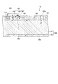
- FIG. 9 shows a configuration of an X-ray detector 1010 configured similarly to the SDD disclosed in Patent Document 1 or Patent Document 2.
- FIG. 9 shows a cross section of the X-ray detector 1010. As shown in FIG. 9, the X-ray detector 1010 has a semiconductor substrate 1100.
- the semiconductor substrate 1100 has a semiconductor layer 1101, an anode electrode 1110, a cathode electrode 1120, and a plurality of regions 1130.
- the reference numeral of one region 1130 is shown as a representative of the plurality of regions 1130.
- the semiconductor substrate 1100 has a surface 1100a and a surface 1100b.
- the surface 1100a and the surface 1100b face in opposite directions.
- the semiconductor layer 1101 includes an N-type semiconductor.
- the anode electrode 1110 and the plurality of regions 1130 are provided in the semiconductor layer 1101.
- Anode electrode 1110 includes an N-type semiconductor.
- the impurity concentration of the anode electrode 1110 is higher than the impurity concentration of the semiconductor layer 1101.
- the region 1130 includes a P-type semiconductor.
- the anode electrode 1110 and the plurality of regions 1130 include a surface 1100a.
- Each of the anode electrode 1110 and the plurality of regions 1130 is a semiconductor region from the surface 1100a to a predetermined depth.
- the cathode electrode 1120 is disposed on the semiconductor layer 1101.
- Cathode electrode 1120 includes a P-type semiconductor.
- Cathode electrode 1120 includes a surface 1100b.
- Cathode electrode 1120 is a semiconductor region from surface 1100b to a predetermined depth.
- a terminal for outputting a signal from the anode electrode 1110 may be provided on the anode electrode 1110.
- a terminal for applying a voltage to the cathode electrode 1120 may be provided on the cathode electrode 1120.
- a plurality of gate electrodes are arranged on surface 1100a. The gate electrode and the region 1130 form a MOSFET (Metal Oxide Semiconductor Semiconductor Field Effect Transistor).
- FIG. 10 is a plan view of the X-ray detector 1010.
- FIG. 10 shows each element when the X-ray detector 1010 is viewed in a direction perpendicular to the surface 1100a of the semiconductor substrate 1100. That is, FIG. 10 shows each element when the X-ray detector 1010 is viewed from the front of the semiconductor substrate 1100.
- the reference numeral of one area 1130 is shown as a representative of the plurality of areas 1130.
- Anode electrode 1110 is arranged at the center of surface 1100a of semiconductor substrate 1100.
- the anode electrode 1110 is circular.
- the plurality of regions 1130 are ring-shaped.
- the plurality of regions 1130 are arranged concentrically.
- the plurality of regions 1130 are arranged so as to surround the anode electrode 1110.
- a cross section taken along line L10 shown in FIG. 10 is shown in FIG.
- a negative voltage is applied to the cathode electrode 1120.
- the absolute value of the voltage applied to cathode electrode 1120 is larger than the absolute value of the voltage of anode electrode 1110.
- the potential inside semiconductor substrate 1100 increases from surface 1100b toward surface 1100a.
- a negative voltage is applied to the gate electrode on surface 1100a.
- the potential of the anode electrode 1110 is higher than any potential of the plurality of gate electrodes.
- the absolute value of the voltage applied to the outer gate electrode is larger than the absolute value of the voltage applied to the inner gate electrode. Therefore, the absolute value of the voltage applied to the outer region 1130 is larger than the absolute value of the voltage applied to the inner region 1130.
- the potential inside semiconductor substrate 1100 increases from the outer periphery of semiconductor substrate 1100 toward the center.
- the voltage as described above is applied to the X-ray detector 1010.
- the potential in the semiconductor substrate 1100 increases from the surface 1100b toward the surface 1100a, and increases from the outer periphery of the semiconductor substrate 1100 toward the center. That is, a potential gradient is generated in the semiconductor substrate 1100.
- X-rays enter the X-ray detector 1010, electrons are generated in the semiconductor substrate 1100. The electrons gather on the anode electrode 1110 according to the potential gradient. A signal based on the electrons is output from X-ray detector 1010.
- a chip having a first-stage amplifier is used to convert the electric charge into a voltage signal.
- the chip having the first-stage amplifier is different from the chip having the X-ray detector.
- the first-stage amplifier is composed of a JFET (Junction Field Effect Transistor) or the like.
- this method requires a wire containing aluminum or gold between the X-ray detector and the first-stage amplifier.
- the wires increase the components of capacitance, resistance, and inductor, and increase noise.
- a technique for forming a JFET at the center of an X-ray detector is known.
- a JFET is arranged at the center of the X-ray detector, and an anode electrode is arranged around the JFET.
- the anode electrode has a ring shape.
- the peripheral length of the anode electrode is larger than in the technique in which the anode electrode is arranged at the center of the X-ray detector. Therefore, the parasitic capacitance on the anode electrode increases, and noise increases.
- An object of the present invention is to provide an X-ray detector capable of suppressing an increase in noise.
- an X-ray detector has a semiconductor substrate, a first electrode, and a second electrode.
- the semiconductor substrate has a first main surface and a second main surface facing in opposite directions.
- the first electrode is arranged on the first main surface, and collects electric charges generated in the semiconductor substrate when X-rays are incident on the semiconductor substrate.
- the second electrode is disposed on the second main surface.
- a voltage for moving the charge in the direction of the first electrode is applied to the second electrode.
- the semiconductor substrate has a third electrode and a transistor.
- the third electrode is arranged in the semiconductor substrate and forms a part of the first main surface.
- a voltage for moving the charge in the direction of the first electrode is applied to the third electrode.
- the transistor has a source, a drain, and a gate. The source and the drain are disposed in the third electrode.
- the gate is disposed on the first main surface and is connected to the first electrode.
- the absolute value of the voltage may be 10 V or less.
- the X-ray detector may include a plurality of the first electrodes and a plurality of the third electrodes.
- the source and the drain may be arranged in the third electrode closest to the first electrode.
- the first voltage may be applied as the voltage to the third electrode on which the transistor is arranged.
- a second voltage may be applied as the voltage to the third electrode where the transistor is not provided.
- the absolute value of the first voltage may be smaller than the absolute value of the second voltage.
- the third electrode may extend from the first main surface to a first position.
- the first position may be separated from the first main surface by a first distance toward the inside of the semiconductor substrate.
- the first electrode may extend from the first main surface to a second position.
- the second position may be separated from the first main surface by a second distance toward the inside of the semiconductor substrate. The first distance may be greater than the second distance.
- the plurality of third electrodes are arranged as a first part and the third electrode arranged as a second part. And the third electrode.
- the first portion may extend from the first main surface to a third position.
- the third position may be separated from the first main surface by a third distance toward the inside of the semiconductor substrate.
- the second portion may extend from the first main surface to a fourth position.
- the fourth position may be separated from the first main surface by a fourth distance toward the inside of the semiconductor substrate.
- the third distance may be greater than the fourth distance.
- the second portion may be arranged between the first electrode and the first portion.
- the source and the drain may be arranged in the second portion.
- the X-ray detector may further include a fourth electrode.
- the fourth electrode may extend from a fifth position to a sixth position.
- the fifth position may be separated from the second main surface by a fifth distance toward the inside of the semiconductor substrate.
- the sixth position may be separated from the second main surface by a sixth distance toward the inside of the semiconductor substrate. The sixth distance may be greater than the fifth distance.
- the second electrode may extend from the second main surface to the fifth position.
- the X-ray detector can suppress an increase in noise.
- FIG. 2 is a sectional view of the X-ray detector according to the first embodiment of the present invention. It is a top view of the X-ray detector of a 1st embodiment of the present invention. It is a sectional view of an X-ray detector of a 2nd embodiment of the present invention. It is sectional drawing of the X-ray detector of 3rd Embodiment of this invention. It is sectional drawing of the X-ray detector of the 1st modification of 3rd Embodiment of this invention. It is sectional drawing of the X-ray detector of the 2nd modification of 3rd Embodiment of this invention. It is a top view of the X-ray detector of a 4th embodiment of the present invention. It is a top view of the X-ray detector of a modification of a 4th embodiment of the present invention. It is sectional drawing of the X-ray detector of a prior art. It is a top view of a conventional X-ray detector.
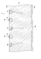
- FIG. 1 shows a configuration of an X-ray detector 10 according to a first embodiment of the present invention.
- FIG. 1 shows a cross section of the X-ray detector 10.
- the X-ray detector 10 is configured as a silicon drift detector (SDD) that detects radiation, that is, fluorescent X-rays.
- SDD silicon drift detector
- the dimensions of the parts constituting the X-ray detector 10 do not always follow the dimensions shown in FIG.
- the dimensions of the parts constituting the X-ray detector 10 may be arbitrary. The same applies to dimensions in other sectional views.
- the X-ray detector 10 has a semiconductor substrate 100, an anode electrode 110 (first electrode), and a cathode electrode 120 (second electrode).
- Semiconductor substrate 100 has a surface 100a (first main surface) and a surface 100b (second main surface) that face in opposite directions.
- the anode electrode 110 is disposed on the surface 100a, and collects charges generated in the semiconductor substrate 100 when X-rays enter the semiconductor substrate 100.
- Cathode electrode 120 is arranged on surface 100b. A voltage for moving the charges in the direction of the anode electrode 110 is applied to the cathode electrode 120.
- the semiconductor substrate 100 includes a region 130 (third electrode) and a transistor 140.
- the region 130 is arranged in the semiconductor substrate 100 and forms a part of the surface 100a.
- a voltage for moving charges in the direction of the anode electrode 110 is applied to the region 130.
- the transistor 140 has a source 141, a drain 142, and a gate 143. Source 141 and drain 142 are arranged in region 130.
- Gate 143 is arranged on surface 100a. Gate 143 is connected to anode electrode 110.
- the semiconductor substrate 100 has a semiconductor layer 101, an anode electrode 110, a cathode electrode 120, and a plurality of regions 130.
- the semiconductor material forming the semiconductor substrate 100 is silicon (Si).
- Surface 100a and surface 100b constitute a main surface of semiconductor substrate 100.
- the main surface is a relatively wide surface among a plurality of surfaces constituting the surface of the semiconductor substrate 100.
- the semiconductor layer 101 includes an N-type semiconductor.
- the anode electrode 110 and the plurality of regions 130 are arranged on the semiconductor layer 101.
- Anode electrode 110 includes an N-type semiconductor.
- the impurity concentration of the anode electrode 110 is higher than the impurity concentration of the semiconductor layer 101.
- the region 130 includes a P-type semiconductor.
- Anode electrode 110 and region 130 include surface 100a. Each of anode electrode 110 and region 130 is a semiconductor region from surface 100a to a predetermined depth. The area 130 extends from the surface 100a to a predetermined position. The predetermined position is separated from the surface 100a toward the inside of the semiconductor substrate 100 by a distance d1. The distance d1 is the depth of the region 130.
- the transistor 140 is a MOSFET.
- the source 141 and the drain 142 are arranged in the region 130 closest to the anode electrode 110.
- Source 141 and drain 142 are arranged in region 130 adjacent to anode electrode 110.
- the region 130 where the source 141 is disposed is the same as the region 130 where the drain 142 is disposed.
- a drain 142 is arranged on a side closer to the anode electrode 110, and a source 141 is arranged on a side farther from the anode electrode 110.
- the drain 142 is disposed between the anode electrode 110 and the source 141.
- the source 141 and the drain 142 include an N-type semiconductor.
- Source 141 and drain 142 include surface 100a. Each of source 141 and drain 142 is a semiconductor region from surface 100a to a predetermined depth.
- the source 141 extends from the surface 100a to a predetermined position. The predetermined position of the source 141 is away from the surface 100a by a distance d2 toward the inside of the semiconductor substrate 100.
- the drain 142 extends from the surface 100a to a predetermined position.
- the predetermined position of the drain 142 is away from the surface 100a by a distance d3 toward the inside of the semiconductor substrate 100.
- the distance d2 is the same as the distance d3.
- the distance d2 may be different from the distance d3.
- the distance d2 and the distance d3 are smaller than the distance d1.
- the distance d2 is the depth of the source 141.
- the distance d3 is the depth of the drain 142.
- An insulating layer 150 is arranged on a region between the source 141 and the drain 142.
- the insulating layer 150 is made of an insulating material.
- the insulating material forming the insulating layer 150 is silicon dioxide (SiO2).
- the insulating layer 150 is stacked on the semiconductor layer 101.
- the insulating layer 150 is in contact with the surface 100a.
- the gate 143 is stacked on the insulating layer 150. Gate 143 is connected to anode electrode 110 by wiring 160.
- the region 130 where the gate 143 is arranged is the same as the region 130 where the source 141 and the drain 142 are arranged.
- the source 141 and the drain 142 are connected to a wiring not shown in FIG.
- the source 141 and the drain 142 are electrically connected to a circuit outside the X-ray detector 10.
- the transistor 140 is a circuit element for extracting a signal from the anode electrode 110 and amplifying the signal. By disposing the transistor 140 in the X-ray detector 10, a first-stage amplifier including the transistor 140 can be disposed in the X-ray detector 10.
- the cathode electrode 120 is disposed on the semiconductor layer 101.
- Cathode electrode 120 includes a P-type semiconductor.
- Cathode electrode 120 includes surface 100b.
- Cathode electrode 120 is a semiconductor region from surface 100b to a predetermined depth.
- a terminal for outputting a signal from the anode electrode 110 may be provided on the anode electrode 110.
- a terminal for applying a voltage to the cathode electrode 120 may be disposed on the cathode electrode 120.
- a plurality of gate electrodes are arranged on surface 100a.
- the gate electrode and the region 130 constitute a MOSFET. This MOSFET is a PMOS, and the transistor 140 is an NMOS.
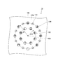
- FIG. 2 is a plan view of the X-ray detector 10.
- FIG. 2 shows each element when the X-ray detector 10 is viewed in a direction perpendicular to the surface 100a of the semiconductor substrate 100. That is, in FIG. 2, each element when the X-ray detector 10 is viewed from the front of the semiconductor substrate 100 is shown.
- the reference numeral of one area 130 is shown as a representative of the plurality of areas 130.
- the outer shape of the X-ray detector 10 is rectangular. In the example shown in FIG. 2, the outer shape of the X-ray detector 10 is a square. The outer shape of the X-ray detector 10 is not limited to a rectangle.
- the anode electrode 110 is arranged at the center of the surface 100 a of the semiconductor substrate 100.
- the anode electrode 110 is circular.
- the outer shape of the anode electrode 110 may be rectangular or the like.
- the plurality of regions 130 are ring-shaped.
- the plurality of regions 130 are arranged concentrically.
- the plurality of regions 130 are arranged so as to surround the anode electrode 110.
- a cross section through the line L1 shown in FIG. 2 is shown in FIG.
- a negative voltage is applied to the cathode electrode 120.
- the absolute value of the voltage applied to the cathode electrode 120 is larger than the absolute value of the voltage of the anode electrode 110.
- the voltage applied to the cathode electrode 120 is from ⁇ 80V to ⁇ 100V.
- the potential inside semiconductor substrate 100 increases from surface 100b toward surface 100a.
- a negative voltage is applied to the gate electrode on the surface 100a.
- the potential of the anode electrode 110 is higher than any potential of the plurality of gate electrodes.
- the absolute value of the voltage applied to the outer gate electrode is larger than the absolute value of the voltage applied to the inner gate electrode. Therefore, the absolute value of the voltage applied to the outer region 130 is larger than the absolute value of the voltage applied to the inner region 130.
- the voltage applied to the outermost region 130 is between -80V and -100V.
- the potential inside the semiconductor substrate 100 increases from the outer periphery to the center of the semiconductor substrate 100.
- the first voltage is applied to the region 130 where the transistor 140 is provided.
- a second voltage is applied to region 130 where transistor 140 is not located.
- the absolute value of the first voltage is smaller than the absolute value of the second voltage.
- a voltage having an absolute value of 10 V or less is applied to the region 130 where the transistor 140 is provided. For example, a voltage in the range of ⁇ 5 V to ⁇ 10 V is applied to the region 130. A voltage in the range of -1V to -10V may be applied to the region 130.
- the voltage as described above is applied to the X-ray detector 10.
- the potential in the semiconductor substrate 100 increases from the surface 100b toward the surface 100a, and increases from the outer periphery to the center of the semiconductor substrate 100. That is, a potential gradient is generated in the semiconductor substrate 100.
- X-rays enter the X-ray detector 10 electrons are generated in the semiconductor substrate 100.
- the electrons gather on the anode electrode 110 according to the potential gradient.
- a signal based on the electrons is extracted by the transistor 140.
- the semiconductor substrate 100 may include a P-type semiconductor.
- the anode electrode 110, the source 141, and the drain 142 include a P-type semiconductor.
- the cathode electrode 120 and the region 130 include an N-type semiconductor.
- a positive voltage is applied to the cathode electrode 120 and the region 130.
- holes are output from the anode electrode 110 as charges.
- the X-ray detector 10 according to the first embodiment has the transistor 140 arranged in the region 130 in the semiconductor substrate 100. Therefore, the peripheral length of the anode electrode 110 does not increase.
- the X-ray detector 10 can suppress an increase in noise caused by the parasitic capacitance of the anode electrode 110.
- the transistor 140 is disposed in the region 130 closest to the anode electrode 110.
- a relatively low voltage (a voltage having a small absolute value) is applied to the region 130 where the transistor 140 is provided. Since the withstand voltage of the transistor 140 is easily ensured, the thickness of the insulating layer 150 can be reduced, and the transistor 140 can be easily formed.
- a plurality of electrons generated by X-rays are not always accelerated uniformly by a potential gradient.
- the speed of the plurality of electrons varies. Therefore, the difference in the time when a plurality of electrons reach the anode electrode in the X-ray detector increases. If the difference is large, the signal output from the anode electrode is processed as noise by the subsequent signal processing circuit. The signal is not suitable for analysis.
- FIG. 3 shows a configuration of the X-ray detector 11 according to the second embodiment of the present invention.
- FIG. 3 shows a cross section of the X-ray detector 11. The description of the same parts as those shown in FIG. 1 is omitted.
- the X-ray detector 11 has a plurality of anode electrodes 110.
- three anode electrodes 110 are shown.
- a region 130 is arranged between two adjacent anode electrodes 110.
- two regions 130 are shown.
- a transistor 140 is provided in each region 130.
- the number of anode electrodes 110 and the number of regions 130 are the same.
- the voltages applied to the plurality of anode electrodes 110 are the same.
- one anode electrode 110 can be made smaller. Therefore, the parasitic capacitance on the anode electrode 110 decreases.
- a plurality of anode electrodes 110 are separated from each other by each region 130.
- a potential gradient is generated in a direction from each region 130 toward the anode electrode 110.
- the electrons move to the anode electrode 110 according to the potential gradient.
- a plurality of electrons included in one electron group are difficult to separate and easily reach one anode electrode 110.
- FIG. 4 shows a configuration of the X-ray detector 12 according to the third embodiment of the present invention.
- FIG. 4 shows a cross section of the X-ray detector 12. The description of the same portions as those shown in FIG. 1 or 3 will be omitted.
- the region 131 extends from the surface 100a to a predetermined position (first position).
- the predetermined position is separated from the surface 100a toward the inside of the semiconductor substrate 100 by a distance d4 (first distance).
- the distance d4 is larger than the distance d1 shown in FIG.
- the anode electrode 110 extends from the surface 100a to a predetermined position (second position).
- the predetermined position is separated from the surface 100a toward the inside of the semiconductor substrate 100 by a distance d5 (second distance).
- the distance d4 is larger than the distance d5.
- the distance d4 is the depth of the region 131.
- the distance d5 is the depth of the anode electrode 110.
- the region 130 shown in FIG. 3 is formed by ion implantation.
- the region 131 shown in FIG. 4 is formed by, for example, the following method. A hole is dug deep into the semiconductor layer 101, and the surface of the hole is covered with an insulating layer. Then, a conductor layer is formed in the hole covered with the insulating layer. When an appropriate voltage is applied to the region 131, an inversion layer is formed at the interface between the insulating layer and the semiconductor layer 101, as in the ON state of the MOSFET. The inversion layer has a polarity opposite to the polarity of the anode electrode 110.
- FIG. 5 shows a configuration of an X-ray detector 13 according to a first modification of the third embodiment of the present invention.
- FIG. 5 shows a cross section of the X-ray detector 13. The description of the same parts as those shown in FIG. 4 will be omitted.
- the area 131 shown in FIG. The transistor 140 is not provided in the region 132.
- An area 130 is arranged in addition to the area 132.
- the transistor 140 is provided in the region 130.
- the region 132 (first portion) extends from the surface 100a to a predetermined position (third position). The predetermined position is away from the surface 100a toward the inside of the semiconductor substrate 100 by a distance d6 (third distance).
- the region 130 (second portion) extends from the surface 100a to a predetermined position (fourth position).
- the predetermined position is separated from the surface 100a by a distance d1 (fourth distance) toward the inside of the semiconductor substrate 100.
- the distance d6 is larger than the distance d1.
- the distance d6 is the depth of the region 132.
- Region 130 is arranged between anode electrode 110 and region 132.
- the region 132 is arranged between two adjacent anode electrodes 110.
- the voltage applied to the region 132 and the voltage applied to the region 130 are different from each other.
- the absolute value of the voltage applied to the region 132 is larger than the absolute value of the voltage applied to the region 130.
- the absolute value of the voltage applied to the cathode electrode 120 can be reduced as in the X-ray detector 12 shown in FIG.
- FIG. 6 shows a configuration of an X-ray detector 14 according to a second modification of the third embodiment of the present invention.
- FIG. 6 shows a cross section of the X-ray detector 14. The description of the same parts as those shown in FIG. 4 will be omitted.
- the X-ray detector 14 further has a plurality of regions 170 (fourth electrodes). In FIG. 6, two regions 170 are shown.
- the region 170 is provided in the semiconductor layer 101.
- Region 170 includes a P-type semiconductor.
- the region 170 is a semiconductor region from the interface between the cathode electrode 120 and the semiconductor layer 101 to a predetermined depth.
- Cathode electrode 120 extends from surface 100b to position P1 (fifth position).
- the position P1 is separated from the surface 100b toward the inside of the semiconductor substrate 100 by a distance d7 (fifth distance).
- the region 170 extends from the position P1 to a position P2 (sixth position).
- the position P2 is separated from the surface 100b toward the inside of the semiconductor substrate 100 by a distance d8 (sixth distance).
- the distance d8 is larger than the distance d7.
- the distance d7 is the depth of the cathode electrode 120.
- the distance d8 is the depth of the region 170.
- the position of the region 170 in the direction Dr1 parallel to the surface 100a and the position of the region 131 in the direction Dr1 are the same.
- the virtual straight line VL1 passes through the region 170 and the region 131.
- the virtual straight line VL1 extends in a direction Dr2 perpendicular to the surface 100a.
- the direction Dr2 is a thickness direction of the semiconductor substrate 100.
- the position of the region 170 in the direction Dr1 and the position of the region 131 in the direction Dr1 may be different.
- Region 170 is connected to cathode electrode 120.
- the voltage applied to cathode electrode 120 is applied to region 170.
- the region 131 and the region 170 may be connected. That is, the region 131 and the region 170 may be formed as layers penetrating the semiconductor substrate 100. At least one of the X-ray detector 10 shown in FIG. 1, the X-ray detector 11 shown in FIG. 3, and the X-ray detector 13 shown in FIG.
- Forming the region 170 deep reduces the area that must be depleted between the region 170 and the region 131. Therefore, the voltage applied to cathode electrode 120 can be reduced. In other words, the absolute value of the voltage applied to the cathode electrode 120 can be reduced.
- FIG. 7 is a plan view of an X-ray detector 15 according to the fourth embodiment of the present invention.
- FIG. 7 shows each element when the X-ray detector 15 is viewed in a direction perpendicular to the surface 100a of the semiconductor substrate 100. That is, in FIG. 7, each element when the X-ray detector 15 is viewed from the front of the semiconductor substrate 100 is shown.
- the X-ray detector 15 has a plurality of anode electrodes 110 and a plurality of regions 130.
- the reference numeral of one anode electrode 110 is shown as a representative of the plurality of anode electrodes 110.
- the reference numeral of one area 130 is shown as a representative of the plurality of areas 130.
- the plurality of anode electrodes 110 are arranged around the area 100c on the surface 100a.
- the plurality of anode electrodes 110 are arranged at equal intervals.
- the distance from the center of the region 100c to the plurality of anode electrodes 110 is the same.
- the plurality of regions 130 extend radially from the center of the region 100c.
- Each region 130 is arranged between two adjacent anode electrodes 110.
- the plurality of anode electrodes 110 and the plurality of regions 130 are arranged symmetrically.
- the transistor 140 is arranged in the portion 130 a of the region 130.
- the portion 130a is disposed between two adjacent anode electrodes 110.
- the plurality of anode electrodes 110 and the plurality of regions 130 are arranged without bias. Therefore, the performance of each of the anode electrodes 110 to detect electrons becomes uniform.
- FIG. 8 is a plan view of an X-ray detector 16 according to a modification of the fourth embodiment of the present invention.
- FIG. 8 shows each element when the X-ray detector 16 is viewed in a direction perpendicular to the surface 100a of the semiconductor substrate 100. That is, FIG. 8 shows each element when the X-ray detector 16 is viewed from the front of the semiconductor substrate 100.
- the X-ray detector 16 has a plurality of anode electrodes 110 and a plurality of regions 130.
- reference numeral of one anode electrode 110 is shown as a representative of the plurality of anode electrodes 110.
- reference numerals of two regions 130 are shown as representatives of the plurality of regions 130.
- the positions of the plurality of anode electrodes 110 are the same as the positions of the plurality of anode electrodes 110 shown in FIG.
- the plurality of regions 130 include a first group of eight regions 130 and a second group of eight regions 130.
- the eight regions 130 of the first group are arranged at positions separated by a distance d9 from the center of the region 100c.
- Each region 130 of the first group is arranged between two adjacent anode electrodes 110.
- the eight regions 130 of the second group are arranged at positions separated by a distance d10 from the center of the region 100c.
- the distance d10 is smaller than the distance d9.
- the eight regions 130 of the first group are arranged at equal intervals.
- the eight regions 130 of the second group are arranged at equal intervals.
- the plurality of anode electrodes 110 and the plurality of regions 130 are arranged symmetrically.
- the transistor 140 is arranged in each region 130 of the first group.
- the plurality of anode electrodes 110 and the plurality of regions 130 are arranged without bias. Therefore, the performance of each of the anode electrodes 110 to detect electrons becomes uniform.
- the X-ray detector can suppress an increase in noise.
Landscapes
- Physics & Mathematics (AREA)
- Health & Medical Sciences (AREA)
- Life Sciences & Earth Sciences (AREA)
- General Physics & Mathematics (AREA)
- High Energy & Nuclear Physics (AREA)
- Molecular Biology (AREA)
- Spectroscopy & Molecular Physics (AREA)
- Measurement Of Radiation (AREA)
Abstract
X線検出器は、半導体基板、第1の電極、および第2の電極を有する。前記第1の電極は、前記半導体基板の第1の主面に配置されている。前記第2の電極は、前記半導体基板の第2の主面に配置されている。前記半導体基板は、第3の電極およびトランジスタを有する。前記第3の電極は、前記半導体基板内に配置され、かつ前記第1の主面の一部を形成し、前記電荷を前記第1の電極の方向へ移動させるための電圧が印加される。前記トランジスタは、ソース、ドレイン、およびゲートを有する。前記ソースおよび前記ドレインは前記第3の電極内に配置されている。前記ゲートは前記第1の主面に配置され、かつ前記第1の電極に接続されている。
Description
本発明は、X線検出器に関する。
X線が金属等の物質に照射されたとき、その物質がその物質の原子に固有のエネルギー(波長)の蛍光を発することが知られている。蛍光の波長帯域はX線の波長帯域とほぼ等しい。蛍光の強度は非常に微弱である。
この現象は、対象物に含まれる金属等の物質の種類および量の推定に応用できる。この推定のために対象物にX線が照射され、かつ対象物から発せられた蛍光X線が観察される。蛍光X線に含まれる光の波長毎のエネルギー強度に基づいて、すなわち蛍光X線のスペクトルに基づいて上記の推定が実行される。
微弱な蛍光X線を効率的に検出するシリコンドリフト検出器(SDD)が開示されている。図9は、特許文献1または特許文献2に開示されたSDDと同様に構成されたX線検出器1010の構成を示す。図9において、X線検出器1010の断面が示されている。図9に示すようにX線検出器1010は、半導体基板1100を有する。
半導体基板1100は、半導体層1101、アノード電極1110、カソード電極1120、および複数の領域1130を有する。図9において、複数の領域1130のうち代表として1つの領域1130の符号が示されている。
半導体基板1100は、面1100aおよび面1100bを有する。面1100aおよび面1100bは、互いに反対方向を向く。
半導体層1101は、N型半導体を含む。アノード電極1110および複数の領域1130は、半導体層1101に配置されている。アノード電極1110は、N型半導体を含む。例えば、アノード電極1110の不純物濃度は、半導体層1101の不純物濃度よりも高い。領域1130は、P型半導体を含む。アノード電極1110および複数の領域1130は、面1100aを含む。アノード電極1110および複数の領域1130の各々は、面1100aから所定の深さまでの半導体領域である。
カソード電極1120は、半導体層1101に配置されている。カソード電極1120は、P型半導体を含む。カソード電極1120は、面1100bを含む。カソード電極1120は、面1100bから所定の深さまでの半導体領域である。
アノード電極1110から信号を出力するための端子がアノード電極1110上に配置されてもよい。カソード電極1120に電圧を印加するための端子がカソード電極1120上に配置されてもよい。複数のゲート電極が面1100a上に配置される。ゲート電極および領域1130は、MOSFET(Metal Oxide Semiconductor Field Effect Transistor)を構成する。
図10は、X線検出器1010の平面図である。図10において、半導体基板1100の面1100aに垂直な方向にX線検出器1010を見たときの各要素が示されている。つまり、図10において、半導体基板1100の正面からX線検出器1010を見たときの各要素が示されている。図10において、複数の領域1130のうち代表として1つの領域1130の符号が示されている。
アノード電極1110は、半導体基板1100の面1100aの中心に配置されている。アノード電極1110は、円形である。複数の領域1130は、リング状である。複数の領域1130は、同心円状に配置されている。複数の領域1130は、アノード電極1110を囲むように配置されている。図10に示す線L10を通る断面が図9に示されている。
負電圧がカソード電極1120に印加される。カソード電極1120に印加される電圧の絶対値は、アノード電極1110の電圧の絶対値よりも大きい。半導体基板1100の内部の電位は、面1100bから面1100aに向かって高くなる。
負電圧が面1100a上のゲート電極に印加される。アノード電極1110の電位は、複数のゲート電極のどの電位よりも高い。より外側のゲート電極に印加される電圧の絶対値は、より内側のゲート電極に印加される電圧の絶対値よりも大きい。そのため、より外側の領域1130に印加される電圧の絶対値は、より内側の領域1130に印加される電圧の絶対値よりも大きい。半導体基板1100の内部の電位は、半導体基板1100の外周から中心に向かって高くなる。
上記のような電圧がX線検出器1010に印加される。半導体基板1100内の電位は、面1100bから面1100aに向かって高くなり、かつ半導体基板1100の外周から中心に向かって高くなる。つまり、電位勾配が半導体基板1100に発生する。X線がX線検出器1010に入射した場合、半導体基板1100において電子が発生する。その電子は、電位勾配に従ってアノード電極1110に集まる。その電子に基づく信号がX線検出器1010から出力される。
X線検出器において、X線検出器に入射したX線のエネルギーに比例した数の電荷が発生する。その電荷を電圧信号に変換するために、初段アンプを有するチップが使用されている。初段アンプを有するチップは、X線検出器を有するチップとは異なる。初段アンプは、JFET(Junction Field Effect Transistor)などで構成されている。
しかし、この方法では、X線検出器と初段アンプとの間に、アルミまたは金などを含むワイヤが必要である。ワイヤにより容量、抵抗、およびインダクタの各々の成分が増加し、かつ雑音が増加する。この問題を解決するために、X線検出器の中心にJFETを形成する技術が知られている。
この技術では、X線検出器の中心にJFETが配置され、かつJFETの周囲にアノード電極が配置される。アノード電極はリング状である。この技術では、アノード電極をX線検出器の中心に配置する技術と比較して、アノード電極の周囲長が大きくなる。そのため、アノード電極に寄生する容量が大きくなり、かつ雑音が増加する。
本発明は、雑音の増加を抑えることができるX線検出器を提供することを目的とする。
本発明の第1の態様によれば、X線検出器は、半導体基板、第1の電極、および第2の電極を有する。前記半導体基板は、互いに反対方向を向く第1の主面および第2の主面を有する。前記第1の電極は、前記第1の主面に配置され、かつX線が前記半導体基板に入射したときに前記半導体基板内で発生した電荷を収集する。前記第2の電極は、前記第2の主面に配置されている。前記電荷を前記第1の電極の方向へ移動させるための電圧が前記第2の電極に印加される。前記半導体基板は、第3の電極およびトランジスタを有する。前記第3の電極は、前記半導体基板内に配置され、かつ前記第1の主面の一部を形成する。前記電荷を前記第1の電極の方向へ移動させるための電圧が前記第3の電極に印加される。前記トランジスタは、ソース、ドレイン、およびゲートを有する。前記ソースおよび前記ドレインが前記第3の電極内に配置されている。前記ゲートが前記第1の主面に配置され、かつ前記第1の電極に接続されている。
本発明の第2の態様によれば、第1の態様において、前記電圧の絶対値は10V以下であってもよい。
本発明の第3の態様によれば、第1の態様において、前記X線検出器は、複数の前記第1の電極および複数の前記第3の電極を有してもよい。
本発明の第4の態様によれば、第3の態様において、前記ソースおよび前記ドレインは、前記第1の電極に最も近い前記第3の電極内に配置されてもよい。
本発明の第5の態様によれば、第3の態様において、第1の電圧が前記電圧として、前記トランジスタが配置された前記第3の電極に印加されてもよい。第2の電圧が前記電圧として、前記トランジスタが配置されていない前記第3の電極に印加されてもよい。前記第1の電圧の絶対値は、前記第2の電圧の絶対値よりも小さくてもよい。
本発明の第6の態様によれば、第1の態様において、前記第3の電極は、前記第1の主面から第1の位置まで広がってもよい。前記第1の位置は、前記第1の主面から第1の距離だけ前記半導体基板の内部に向かって離れてもよい。前記第1の電極は、前記第1の主面から第2の位置まで広がってもよい。前記第2の位置は、前記第1の主面から第2の距離だけ前記半導体基板の内部に向かって離れてもよい。前記第1の距離は、前記第2の距離よりも大きくてもよい。
本発明の第7の態様によれば、第3の態様において、前記複数の前記第3の電極は、第1の部分として配置された前記第3の電極と、第2の部分として配置された前記第3の電極とを含んでもよい。前記第1の部分は、前記第1の主面から第3の位置まで広がってもよい。前記第3の位置は、前記第1の主面から第3の距離だけ前記半導体基板の内部に向かって離れてもよい。前記第2の部分は、前記第1の主面から第4の位置まで広がってもよい。前記第4の位置は、前記第1の主面から第4の距離だけ前記半導体基板の内部に向かって離れてもよい。前記第3の距離は、前記第4の距離よりも大きくてもよい。
本発明の第8の態様によれば、第7の態様において、前記第2の部分は、前記第1の電極と前記第1の部分との間に配置されてもよい。
本発明の第9の態様によれば、第7の態様において、前記ソースおよび前記ドレインは、前記第2の部分内に配置されてもよい。
本発明の第10の態様によれば、第1の態様において、前記X線検出器は、第4の電極をさらに有してもよい。前記第4の電極は、第5の位置から第6の位置まで広がってもよい。前記第5の位置は、前記第2の主面から第5の距離だけ前記半導体基板の内部に向かって離れてもよい。前記第6の位置は、前記第2の主面から第6の距離だけ前記半導体基板の内部に向かって離れてもよい。前記第6の距離は、前記第5の距離よりも大きくてもよい。前記第2の電極は、前記第2の主面から前記第5の位置まで広がってもよい。
上記の各態様によれば、X線検出器は雑音の増加を抑えることができる。
図面を参照し、本発明の実施形態を説明する。
(第1の実施形態)
図1は、本発明の第1の実施形態のX線検出器10の構成を示す。図1において、X線検出器10の断面が示されている。X線検出器10は、放射線すなわち蛍光X線を検出するシリコンドリフト検出器(SDD)として構成されている。
図1は、本発明の第1の実施形態のX線検出器10の構成を示す。図1において、X線検出器10の断面が示されている。X線検出器10は、放射線すなわち蛍光X線を検出するシリコンドリフト検出器(SDD)として構成されている。
X線検出器10を構成する部分の寸法は、図1に示される寸法に従うとは限らない。X線検出器10を構成する部分の寸法は任意であってよい。他の断面図における寸法についても同様である。
X線検出器10の概略構成について説明する。X線検出器10は、半導体基板100、アノード電極110(第1の電極)、およびカソード電極120(第2の電極)を有する。半導体基板100は、互いに反対方向を向く面100a(第1の主面)および面100b(第2の主面)を有する。アノード電極110は、面100aに配置され、かつX線が半導体基板100に入射したときに半導体基板100内で発生した電荷を収集する。カソード電極120は、面100bに配置されている。電荷をアノード電極110の方向へ移動させるための電圧がカソード電極120に印加される。半導体基板100は、領域130(第3の電極)およびトランジスタ140を有する。領域130は、半導体基板100内に配置され、かつ面100aの一部を形成する。電荷をアノード電極110の方向へ移動させるための電圧が領域130に印加される。トランジスタ140は、ソース141、ドレイン142、およびゲート143を有する。ソース141およびドレイン142は領域130内に配置されている。ゲート143は面100aに配置されている。ゲート143はアノード電極110に接続されている。
X線検出器10の詳細な構成について説明する。半導体基板100は、半導体層101、アノード電極110、カソード電極120、および複数の領域130を有する。例えば、半導体基板100を構成する半導体材料は、シリコン(Si)である。
面100aおよび面100bは、半導体基板100の主面を構成する。主面は、半導体基板100の表面を構成する複数の面のうち相対的に広い面である。
半導体層101は、N型半導体を含む。アノード電極110および複数の領域130は、半導体層101に配置されている。アノード電極110は、N型半導体を含む。例えば、アノード電極110の不純物濃度は、半導体層101の不純物濃度よりも高い。領域130は、P型半導体を含む。
アノード電極110および領域130は、面100aを含む。アノード電極110および領域130の各々は、面100aから所定の深さまでの半導体領域である。領域130は、面100aから所定の位置まで広がっている。所定の位置は、面100aから距離d1だけ半導体基板100の内部に向かって離れている。距離d1は、領域130の深さである。
トランジスタ140は、MOSFETである。ソース141およびドレイン142は、アノード電極110に最も近い領域130内に配置されている。ソース141およびドレイン142は、アノード電極110に隣接する領域130内に配置されている。ソース141が配置された領域130と、ドレイン142が配置された領域130とは、同じである。アノード電極110に近い側にドレイン142が配置され、かつアノード電極110から遠い側にソース141が配置されている。ドレイン142は、アノード電極110とソース141との間に配置されている。
ソース141およびドレイン142は、N型半導体を含む。ソース141およびドレイン142は、面100aを含む。ソース141およびドレイン142の各々は、面100aから所定の深さまでの半導体領域である。ソース141は、面100aから所定の位置まで広がっている。ソース141のその所定の位置は、面100aから距離d2だけ半導体基板100の内部に向かって離れている。ドレイン142は、面100aから所定の位置まで広がっている。ドレイン142のその所定の位置は、面100aから距離d3だけ半導体基板100の内部に向かって離れている。距離d2は、距離d3と同じである。距離d2は、距離d3と異なってもよい。距離d2および距離d3は、距離d1よりも小さい。距離d2は、ソース141の深さである。距離d3は、ドレイン142の深さである。
ソース141およびドレイン142の間の領域上に絶縁層150が配置されている。絶縁層150は、絶縁材料で構成されている。例えば、絶縁層150を構成する絶縁材料は、二酸化珪素(SiO2)である。絶縁層150は、半導体層101に積層されている。絶縁層150は、面100aと接触している。ゲート143は、絶縁層150に積層されている。ゲート143は、配線160によってアノード電極110に接続されている。ゲート143が配置された領域130と、ソース141およびドレイン142が配置された領域130とは、同じである。
ソース141およびドレイン142は、図1に示されていない配線に接続されている。ソース141およびドレイン142は、X線検出器10の外部の回路に電気的に接続されている。トランジスタ140は、アノード電極110から信号を取り出し、かつ増幅するための回路素子である。トランジスタ140をX線検出器10に配置することにより、トランジスタ140を含む初段アンプをX線検出器10に配置することができる。
カソード電極120は、半導体層101に配置されている。カソード電極120は、P型半導体を含む。カソード電極120は、面100bを含む。カソード電極120は、面100bから所定の深さまでの半導体領域である。
アノード電極110から信号を出力するための端子がアノード電極110上に配置されてもよい。カソード電極120に電圧を印加するための端子がカソード電極120上に配置されてもよい。複数のゲート電極が面100a上に配置される。ゲート電極および領域130は、MOSFETを構成する。このMOSFETはPMOSであり、トランジスタ140はNMOSである。
図2は、X線検出器10の平面図である。図2において、半導体基板100の面100aに垂直な方向にX線検出器10を見たときの各要素が示されている。つまり、図2において、半導体基板100の正面からX線検出器10を見たときの各要素が示されている。図2において、複数の領域130のうち代表として1つの領域130の符号が示されている。
X線検出器10の外形は矩形である。図2に示す例では、X線検出器10の外形は正方形である。X線検出器10の外形は、矩形に限らない。
アノード電極110は、半導体基板100の面100aの中心に配置されている。アノード電極110は、円形である。アノード電極110の外形は、矩形等であってもよい。複数の領域130は、リング状である。複数の領域130は、同心円状に配置されている。複数の領域130は、アノード電極110を囲むように配置されている。図2に示す線L1を通る断面が図1に示されている。
負電圧がカソード電極120に印加される。カソード電極120に印加される電圧の絶対値は、アノード電極110の電圧の絶対値よりも大きい。例えば、カソード電極120に印加される電圧は、-80Vから-100Vである。半導体基板100の内部の電位は、面100bから面100aに向かって高くなる。
負電圧が面100a上のゲート電極に印加される。アノード電極110の電位は、複数のゲート電極のどの電位よりも高い。より外側のゲート電極に印加される電圧の絶対値は、より内側のゲート電極に印加される電圧の絶対値よりも大きい。そのため、より外側の領域130に印加される電圧の絶対値は、より内側の領域130に印加される電圧の絶対値よりも大きい。例えば、最も外側の領域130に印加される電圧は、-80Vから-100Vである。半導体基板100の内部の電位は、半導体基板100の外周から中心に向かって高くなる。
第1の電圧が、トランジスタ140が配置された領域130に印加される。第2の電圧が、トランジスタ140が配置されていない領域130に印加される。第1の電圧の絶対値は、第2の電圧の絶対値よりも小さい。
絶対値が10V以下である電圧が、トランジスタ140が配置された領域130に印加される。例えば、-5Vから-10Vの範囲に含まれる電圧がその領域130に印加される。-1Vから-10Vの範囲に含まれる電圧がその領域130に印加されてもよい。
上記のような電圧がX線検出器10に印加される。半導体基板100内の電位は、面100bから面100aに向かって高くなり、かつ半導体基板100の外周から中心に向かって高くなる。つまり、電位勾配が半導体基板100に発生する。X線がX線検出器10に入射した場合、半導体基板100において電子が発生する。その電子は、電位勾配に従ってアノード電極110に集まる。その電子に基づく信号がトランジスタ140によって取り出される。
半導体基板100がP型半導体を含んでもよい。その場合、アノード電極110、ソース141、およびドレイン142は、P型半導体を含む。その場合、カソード電極120および領域130は、N型半導体を含む。その場合、正電圧がカソード電極120および領域130に印加される。その場合、正孔が電荷としてアノード電極110から出力される。
第1の実施形態のX線検出器10は、半導体基板100内の領域130に配置されたトランジスタ140を有する。そのため、アノード電極110の周囲長は大きくならない。X線検出器10は、アノード電極110に寄生する容量を原因とする雑音の増加を抑えることができる。
トランジスタ140は、アノード電極110に最も近い領域130に配置されている。トランジスタ140が配置された領域130には、比較的低い電圧(絶対値が小さな電圧)が印加される。トランジスタ140の耐圧が確保されやすいため、絶縁層150を薄くすることができ、かつトランジスタ140の形成が容易である。
(第2の実施形態)
X線によって発生する複数の電子は、電位勾配によって均等に加速されるとは限らない。複数の電子の速度にはばらつきが発生する。そのため、X線検出器において複数の電子がアノード電極に到達する時間の違いが大きくなる。その違いが大きい場合、アノード電極から出力された信号は、後段の信号処理回路によって雑音として処理される。その信号は分析に適していない。
X線によって発生する複数の電子は、電位勾配によって均等に加速されるとは限らない。複数の電子の速度にはばらつきが発生する。そのため、X線検出器において複数の電子がアノード電極に到達する時間の違いが大きくなる。その違いが大きい場合、アノード電極から出力された信号は、後段の信号処理回路によって雑音として処理される。その信号は分析に適していない。
速度のばらつきが大きな複数の電子を分析に使用するためには、後段の信号処理回路における信号検出の待ち時間(シェーピング時間)を長く設定する必要がある。長いシェーピング時間が設定された場合、検出レートが低下する。そのため、分析装置の性能が低下する。より大きなX線検出器において、この問題は顕著である。
図3は、本発明の第2の実施形態のX線検出器11の構成を示す。図3において、X線検出器11の断面が示されている。図1に示す部分と同じ部分の説明を省略する。
X線検出器11は、複数のアノード電極110を有する。図3において、3つのアノード電極110が示されている。隣接する2つのアノード電極110の間に領域130が配置されている。図3において、2つの領域130が示されている。トランジスタ140が各領域130に配置されている。例えば、アノード電極110の数と領域130の数とは同じである。例えば、複数のアノード電極110に印加される電圧は同じである。
X線が半導体基板100に入射したとき、複数の電子が発生する。各電子は、各電子に近いアノード電極110に向かって移動する。半導体基板100の中心部で発生した電子の移動距離と、半導体基板100の周辺部で発生した電子の移動距離との差が小さくなる。各電子がアノード電極110に到達する時間は、電子の速度のばらつきに依存する。この時間のばらつきは低減される。そのため、シェーピング時間を長く設定することなく、X線により発生した電子の量に応じた信号を検出することができる。
複数のアノード電極110を配置することにより、1つのアノード電極110を小さくすることができる。そのため、アノード電極110に寄生する容量が小さくなる。
各領域130によって、複数のアノード電極110は互いに分離される。各領域130からアノード電極110に向かう方向に電位勾配が発生する。電子は、その電位勾配に従ってアノード電極110に移動する。1つの電子群に含まれる複数の電子は分離しにくく、1つのアノード電極110に到達しやすい。
複数のX線の波がほぼ同時にX線検出器に入射したとき、2つ以上の電子群がほぼ同時に発生する。2つ以上の電子群が1つのアノード電極110にほぼ同時に到達した場合、信号が、1つのX線の波に対応する信号として誤って検出される。この現象は、パイルアップと呼ばれる。複数のアノード電極110を配置し、かつ領域130を各アノード電極110間に配置することにより、2つ以上の電子群がそれぞれ異なるアノード電極110に到達する可能性が高まる。各アノード電極110に対応するトランジスタ140を配置することにより、各電子群に基づく信号を各トランジスタ140によって取り出すことができる。そのため、パイルアップの発生頻度が低下する。
(第3の実施形態)
図4は、本発明の第3の実施形態のX線検出器12の構成を示す。図4において、X線検出器12の断面が示されている。図1または図3に示す部分と同じ部分の説明を省略する。
図4は、本発明の第3の実施形態のX線検出器12の構成を示す。図4において、X線検出器12の断面が示されている。図1または図3に示す部分と同じ部分の説明を省略する。
図3に示す領域130は領域131に変更される。領域131は、面100aから所定の位置(第1の位置)まで広がっている。所定の位置は、面100aから距離d4(第1の距離)だけ半導体基板100の内部に向かって離れている。距離d4は、図1に示す距離d1よりも大きい。アノード電極110は、面100aから所定の位置(第2の位置)まで広がっている。所定の位置は、面100aから距離d5(第2の距離)だけ半導体基板100の内部に向かって離れている。距離d4は、距離d5よりも大きい。距離d4は、領域131の深さである。距離d5はアノード電極110の深さである。
例えば、図3に示す領域130は、イオン注入により形成される。一方、図4に示す領域131は、例えば以下の方法により形成される。半導体層101の深い位置まで穴を掘り、穴の表面が絶縁層で覆われる。その後、絶縁層で覆われた穴に導体層が形成される。適切な電圧が領域131に印加されたとき、MOSFETのオン状態と同様に、反転層が絶縁層と半導体層101との界面に形成される。反転層は、アノード電極110の極性とは逆の極性を持つ。
所定の電圧が領域131に印加されたとき、アノード電極110と領域131との間の領域は完全に空乏化される。空乏化された領域のキャリア濃度は非常に小さい。領域131を深く形成することにより、カソード電極120と領域131との間で空乏化しなければならない範囲が減少する。そのため、カソード電極120に印加する電圧を低くすることができる。言い換えると、カソード電極120に印加する電圧の絶対値を小さくすることができる。
(第3の実施形態の第1の変形例)
図5は、本発明の第3の実施形態の第1の変形例のX線検出器13の構成を示す。図5において、X線検出器13の断面が示されている。図4に示す部分と同じ部分の説明を省略する。
図5は、本発明の第3の実施形態の第1の変形例のX線検出器13の構成を示す。図5において、X線検出器13の断面が示されている。図4に示す部分と同じ部分の説明を省略する。
図4に示す領域131は領域132に変更される。トランジスタ140は領域132に配置されていない。領域132に加えて領域130が配置されている。トランジスタ140は、領域130に配置されている。領域132(第1の部分)は、面100aから所定の位置(第3の位置)まで広がっている。所定の位置は、面100aから距離d6(第3の距離)だけ半導体基板100の内部に向かって離れている。領域130(第2の部分)は、面100aから所定の位置(第4の位置)まで広がっている。所定の位置は、面100aから距離d1(第4の距離)だけ半導体基板100の内部に向かって離れている。距離d6は、距離d1よりも大きい。距離d6は、領域132の深さである。
領域130は、アノード電極110と領域132との間に配置されている。領域132は、隣接する2つのアノード電極110の間に配置されている。
領域132に印加される電圧と、領域130に印加される電圧とは、互いに異なる。領域132に印加される電圧の絶対値は、領域130に印加される電圧の絶対値よりも大きい。
X線検出器13において、図4に示すX線検出器12と同様に、カソード電極120に印加する電圧の絶対値を小さくすることができる。
(第3の実施形態の第2の変形例)
図6は、本発明の第3の実施形態の第2の変形例のX線検出器14の構成を示す。図6において、X線検出器14の断面が示されている。図4に示す部分と同じ部分の説明を省略する。
図6は、本発明の第3の実施形態の第2の変形例のX線検出器14の構成を示す。図6において、X線検出器14の断面が示されている。図4に示す部分と同じ部分の説明を省略する。
X線検出器14は、複数の領域170(第4の電極)をさらに有する。図6において、2つの領域170が示されている。領域170は、半導体層101に配置されている。領域170は、P型半導体を含む。
領域170は、カソード電極120と半導体層101との界面から所定の深さまでの半導体領域である。カソード電極120は、面100bから位置P1(第5の位置)まで広がっている。位置P1は、面100bから距離d7(第5の距離)だけ半導体基板100の内部に向かって離れている。領域170は、位置P1から位置P2(第6の位置)まで広がっている。位置P2は、面100bから距離d8(第6の距離)だけ半導体基板100の内部に向かって離れている。距離d8は、距離d7よりも大きい。距離d7は、カソード電極120の深さである。距離d8は、領域170の深さである。
面100aに平行な方向Dr1における領域170の位置と、方向Dr1における領域131との位置は、同じである。仮想直線VL1は、領域170および領域131を通る。仮想直線VL1は、面100aに垂直な方向Dr2に伸びる。方向Dr2は、半導体基板100の厚さ方向である。方向Dr1における領域170の位置と、方向Dr1における領域131との位置は、異なってもよい。
領域170は、カソード電極120に接続されている。カソード電極120に印加された電圧は、領域170に印加される。
領域131と領域170とが接続されてもよい。つまり、領域131および領域170は、半導体基板100を貫通する層として形成されてもよい。図1に示すX線検出器10、図3に示すX線検出器11、および図5に示すX線検出器13の少なくとも1つが領域170を有してもよい。
領域170を深く形成することにより、領域170と領域131との間で空乏化しなければならない範囲が減少する。そのため、カソード電極120に印加する電圧を低くすることができる。言い換えると、カソード電極120に印加する電圧の絶対値を小さくすることができる。
(第4の実施形態)
図7は、本発明の第4の実施形態のX線検出器15の平面図である。図7において、半導体基板100の面100aに垂直な方向にX線検出器15を見たときの各要素が示されている。つまり、図7において、半導体基板100の正面からX線検出器15を見たときの各要素が示されている。
図7は、本発明の第4の実施形態のX線検出器15の平面図である。図7において、半導体基板100の面100aに垂直な方向にX線検出器15を見たときの各要素が示されている。つまり、図7において、半導体基板100の正面からX線検出器15を見たときの各要素が示されている。
X線検出器15は、複数のアノード電極110および複数の領域130を有する。図7において、複数のアノード電極110のうち代表として1つのアノード電極110の符号が示されている。図7において、複数の領域130のうち代表として1つの領域130の符号が示されている。
複数のアノード電極110は、面100aの領域100cの周囲に配置されている。複数のアノード電極110は、等間隔に配置されている。領域100cの中心から複数のアノード電極110までの距離は、同じである。複数の領域130は、領域100cの中心から放射状に伸びる。各領域130は、隣接する2つのアノード電極110の間に配置されている。複数のアノード電極110および複数の領域130は、点対象に配置されている。
トランジスタ140は、領域130の部分130aに配置されている。部分130aは、隣接する2つのアノード電極110の間に配置されている。
X線検出器15において、複数のアノード電極110および複数の領域130は、偏らずに配置されている。そのため、各アノード電極110が電子を検出する性能が均等になる。
(第4の実施形態の変形例)
図8は、本発明の第4の実施形態の変形例のX線検出器16の平面図である。図8において、半導体基板100の面100aに垂直な方向にX線検出器16を見たときの各要素が示されている。つまり、図8において、半導体基板100の正面からX線検出器16を見たときの各要素が示されている。
図8は、本発明の第4の実施形態の変形例のX線検出器16の平面図である。図8において、半導体基板100の面100aに垂直な方向にX線検出器16を見たときの各要素が示されている。つまり、図8において、半導体基板100の正面からX線検出器16を見たときの各要素が示されている。
X線検出器16は、複数のアノード電極110および複数の領域130を有する。図8において、複数のアノード電極110のうち代表として1つのアノード電極110の符号が示されている。図8において、複数の領域130のうち代表として2つの領域130の符号が示されている。
複数のアノード電極110の位置は、図7に示す複数のアノード電極110の位置と同じである。複数の領域130は、第1のグループの8個の領域130と、第2のグループの8個の領域130とを含む。第1のグループの8個の領域130は、領域100cの中心から距離d9だけ離れた位置に配置されている。第1のグループの各領域130は、隣接する2つのアノード電極110の間に配置されている。第2のグループの8個の領域130は、領域100cの中心から距離d10だけ離れた位置に配置されている。距離d10は、距離d9よりも小さい。
第1のグループの8個の領域130は、等間隔に配置されている。第2のグループの8個の領域130は、等間隔に配置されている。複数のアノード電極110および複数の領域130は、点対象に配置されている。トランジスタ140は、第1のグループの各領域130に配置されている。
X線検出器16において、複数のアノード電極110および複数の領域130は、偏らずに配置されている。そのため、各アノード電極110が電子を検出する性能が均等になる。
以上、本発明の好ましい実施形態を説明したが、本発明はこれら実施形態およびその変形例に限定されることはない。本発明の趣旨を逸脱しない範囲で、構成の付加、省略、置換、およびその他の変更が可能である。また、本発明は前述した説明によって限定されることはなく、添付のクレームの範囲によってのみ限定される。
本発明の各実施形態によれば、X線検出器は雑音の増加を抑えることができる。
10,11,12,13,14,15,16,1010 X線検出器
100,1100 半導体基板
101,1101 半導体層
110,1110 アノード電極
120,1120 カソード電極
130,131,132,170,1130 領域
140 トランジスタ
141 ソース
142 ドレイン
143 ゲート
150 絶縁層
100,1100 半導体基板
101,1101 半導体層
110,1110 アノード電極
120,1120 カソード電極
130,131,132,170,1130 領域
140 トランジスタ
141 ソース
142 ドレイン
143 ゲート
150 絶縁層
Claims (10)
- 互いに反対方向を向く第1の主面および第2の主面を有する半導体基板と、
前記第1の主面に配置され、かつX線が前記半導体基板に入射したときに前記半導体基板内で発生した電荷を収集する第1の電極と、
前記第2の主面に配置され、かつ前記電荷を前記第1の電極の方向へ移動させるための電圧が印加される第2の電極と、
を有し、
前記半導体基板は、
前記半導体基板内に配置され、かつ前記第1の主面の一部を形成し、前記電荷を前記第1の電極の方向へ移動させるための電圧が印加される第3の電極と、
ソース、ドレイン、およびゲートを有し、前記ソースおよび前記ドレインが前記第3の電極内に配置され、前記ゲートが前記第1の主面に配置され、前記ゲートが前記第1の電極に接続されたトランジスタと、
を有するX線検出器。 - 前記電圧の絶対値は10V以下である
請求項1に記載のX線検出器。 - 複数の前記第1の電極および複数の前記第3の電極を有する
請求項1に記載のX線検出器。 - 前記ソースおよび前記ドレインは、前記第1の電極に最も近い前記第3の電極内に配置されている
請求項3に記載のX線検出器。 - 第1の電圧が前記電圧として、前記トランジスタが配置された前記第3の電極に印加され、
第2の電圧が前記電圧として、前記トランジスタが配置されていない前記第3の電極に印加され、
前記第1の電圧の絶対値は、前記第2の電圧の絶対値よりも小さい
請求項3に記載のX線検出器。 - 前記第3の電極は、前記第1の主面から第1の位置まで広がり、前記第1の位置は、前記第1の主面から第1の距離だけ前記半導体基板の内部に向かって離れており、
前記第1の電極は、前記第1の主面から第2の位置まで広がり、前記第2の位置は、前記第1の主面から第2の距離だけ前記半導体基板の内部に向かって離れており、
前記第1の距離は、前記第2の距離よりも大きい
請求項1に記載のX線検出器。 - 前記複数の前記第3の電極は、
第1の部分として配置された前記第3の電極と、
第2の部分として配置された前記第3の電極と、
を含み、
前記第1の部分は、前記第1の主面から第3の位置まで広がり、前記第3の位置は、前記第1の主面から第3の距離だけ前記半導体基板の内部に向かって離れており、
前記第2の部分は、前記第1の主面から第4の位置まで広がり、前記第4の位置は、前記第1の主面から第4の距離だけ前記半導体基板の内部に向かって離れており、
前記第3の距離は、前記第4の距離よりも大きい
請求項3に記載のX線検出器。 - 前記第2の部分は、前記第1の電極と前記第1の部分との間に配置されている
請求項7に記載のX線検出器。 - 前記ソースおよび前記ドレインは、前記第2の部分内に配置されている
請求項7に記載のX線検出器。 - 第5の位置から第6の位置まで広がり、前記第5の位置は、前記第2の主面から第5の距離だけ前記半導体基板の内部に向かって離れ、前記第6の位置は、前記第2の主面から第6の距離だけ前記半導体基板の内部に向かって離れ、前記第6の距離は、前記第5の距離よりも大きい第4の電極をさらに有し、
前記第2の電極は、前記第2の主面から前記第5の位置まで広がっている
請求項1に記載のX線検出器。
Priority Applications (1)
| Application Number | Priority Date | Filing Date | Title |
|---|---|---|---|
| PCT/JP2018/025235 WO2020008531A1 (ja) | 2018-07-03 | 2018-07-03 | X線検出器 |
Applications Claiming Priority (1)
| Application Number | Priority Date | Filing Date | Title |
|---|---|---|---|
| PCT/JP2018/025235 WO2020008531A1 (ja) | 2018-07-03 | 2018-07-03 | X線検出器 |
Publications (1)
| Publication Number | Publication Date |
|---|---|
| WO2020008531A1 true WO2020008531A1 (ja) | 2020-01-09 |
Family
ID=69059542
Family Applications (1)
| Application Number | Title | Priority Date | Filing Date |
|---|---|---|---|
| PCT/JP2018/025235 Ceased WO2020008531A1 (ja) | 2018-07-03 | 2018-07-03 | X線検出器 |
Country Status (1)
| Country | Link |
|---|---|
| WO (1) | WO2020008531A1 (ja) |
Citations (4)
| Publication number | Priority date | Publication date | Assignee | Title |
|---|---|---|---|---|
| JPH11186285A (ja) * | 1997-12-22 | 1999-07-09 | Rigaku Industrial Co | 半導体装置 |
| JP2008258348A (ja) * | 2007-04-04 | 2008-10-23 | Institute X-Ray Technologies Co Ltd | 放射線検出器 |
| US20090026569A1 (en) * | 2007-07-27 | 2009-01-29 | Shenzhen Skyray Instrument Co., Ltd. | Ultra high-resolution radiation detector (UHRD) and method for fabrication thereof |
| JP2014002155A (ja) * | 2012-06-20 | 2014-01-09 | Oxford Instruments Analytical Oy | 漏れ電流収集構造およびそれを用いた放射線検出器 |
-
2018
- 2018-07-03 WO PCT/JP2018/025235 patent/WO2020008531A1/ja not_active Ceased
Patent Citations (4)
| Publication number | Priority date | Publication date | Assignee | Title |
|---|---|---|---|---|
| JPH11186285A (ja) * | 1997-12-22 | 1999-07-09 | Rigaku Industrial Co | 半導体装置 |
| JP2008258348A (ja) * | 2007-04-04 | 2008-10-23 | Institute X-Ray Technologies Co Ltd | 放射線検出器 |
| US20090026569A1 (en) * | 2007-07-27 | 2009-01-29 | Shenzhen Skyray Instrument Co., Ltd. | Ultra high-resolution radiation detector (UHRD) and method for fabrication thereof |
| JP2014002155A (ja) * | 2012-06-20 | 2014-01-09 | Oxford Instruments Analytical Oy | 漏れ電流収集構造およびそれを用いた放射線検出器 |
Non-Patent Citations (2)
| Title |
|---|
| MATSUURA, HIDEHARU ET AL.: "A new n-channel junction field-effect transistor embedded in the i layer of a pin diode", JAPANESE JOURNAL OF APPLIED PHYSICS, vol. 38, 1999, pages L1015 - L1017, XP000948575, DOI: 10.1143/JJAP.38.L1015 * |
| MATSUURA, HIDEHARU ET AL.: "A new structure of an n-channel junction field-effect transistor embedded in a pin diode for an x-ray detector", JAPANESE JOURNAL OF APPLIED PHYSICS, vol. 37, 1998, pages L115 - L118, XP000824541, DOI: 10.1143/JJAP.37.L115 * |
Similar Documents
| Publication | Publication Date | Title |
|---|---|---|
| US6455858B1 (en) | Semiconductor radiation detector | |
| WO2018061334A1 (ja) | アバランシェフォトダイオード | |
| JP6393347B2 (ja) | 電荷検出増幅器 | |
| US7105827B2 (en) | Semiconductor detector with optimised radiation entry window | |
| US10951174B2 (en) | High-frequency amplifier | |
| IL192209A (en) | Semiconductor radiation detector optimized for detecting visible light | |
| CN105575984B (zh) | 特别用途的背照式光传感器集成电路接地系统 | |
| WO2016143156A1 (ja) | 放射線検出器およびそれを用いた放射線検出装置 | |
| CN101300685A (zh) | 半导体装置及其制造方法 | |
| EP3032281B1 (en) | Semiconductor drift detector for detecting radiation | |
| WO2020008531A1 (ja) | X線検出器 | |
| JP6909057B2 (ja) | 炭化ケイ素半導体装置およびその製造方法 | |
| US11604292B2 (en) | Charge preamplifier device and radiation detecting apparatus comprising the device | |
| JP4267397B2 (ja) | 信号電子検出器 | |
| WO2019123591A1 (ja) | 半導体装置 | |
| CN106328661B (zh) | 一种x射线传感器及其制造方法 | |
| US20250306221A1 (en) | Semiconductor detector | |
| RU2141703C1 (ru) | Способ осуществления внутреннего пропорционального усиления в полупроводниковом детекторе частиц и излучений и устройство для его реализации | |
| WO2020183567A1 (ja) | X線検出装置および蛍光x線分析装置 | |
| RU2583955C1 (ru) | Емкостная моп диодная ячейка фотоприемника-детектора излучений | |
| JP2005043263A (ja) | 信号検出器 | |
| JP2024515298A (ja) | ダイオード放射線センサ | |
| JP6493158B2 (ja) | X線検出器 | |
| US20200220079A1 (en) | Compound semiconductor device | |
| CN119486291A (zh) | 一种双埋氧绝缘体上硅总剂量辐照探测器 |
Legal Events
| Date | Code | Title | Description |
|---|---|---|---|
| 121 | Ep: the epo has been informed by wipo that ep was designated in this application |
Ref document number: 18925210 Country of ref document: EP Kind code of ref document: A1 |
|
| NENP | Non-entry into the national phase |
Ref country code: DE |
|
| 122 | Ep: pct application non-entry in european phase |
Ref document number: 18925210 Country of ref document: EP Kind code of ref document: A1 |
|
| NENP | Non-entry into the national phase |
Ref country code: JP |