WO2020115813A1 - Dispositif à semiconducteur, endoscope, et procédé de fabrication de dispositif à semiconducteur - Google Patents
Dispositif à semiconducteur, endoscope, et procédé de fabrication de dispositif à semiconducteur Download PDFInfo
- Publication number
- WO2020115813A1 WO2020115813A1 PCT/JP2018/044530 JP2018044530W WO2020115813A1 WO 2020115813 A1 WO2020115813 A1 WO 2020115813A1 JP 2018044530 W JP2018044530 W JP 2018044530W WO 2020115813 A1 WO2020115813 A1 WO 2020115813A1
- Authority
- WO
- WIPO (PCT)
- Prior art keywords
- core wire
- terminal
- semiconductor
- wiring
- electrode
- Prior art date
- Legal status (The legal status is an assumption and is not a legal conclusion. Google has not performed a legal analysis and makes no representation as to the accuracy of the status listed.)
- Ceased
Links
Images




Classifications
-
- A—HUMAN NECESSITIES
- A61—MEDICAL OR VETERINARY SCIENCE; HYGIENE
- A61B—DIAGNOSIS; SURGERY; IDENTIFICATION
- A61B1/00—Instruments for performing medical examinations of the interior of cavities or tubes of the body by visual or photographical inspection, e.g. endoscopes; Illuminating arrangements therefor
- A61B1/00064—Constructional details of the endoscope body
- A61B1/0011—Manufacturing of endoscope parts
-
- H—ELECTRICITY
- H04—ELECTRIC COMMUNICATION TECHNIQUE
- H04N—PICTORIAL COMMUNICATION, e.g. TELEVISION
- H04N23/00—Cameras or camera modules comprising electronic image sensors; Control thereof
- H04N23/50—Constructional details
- H04N23/54—Mounting of pick-up tubes, electronic image sensors, deviation or focusing coils
-
- A—HUMAN NECESSITIES
- A61—MEDICAL OR VETERINARY SCIENCE; HYGIENE
- A61B—DIAGNOSIS; SURGERY; IDENTIFICATION
- A61B1/00—Instruments for performing medical examinations of the interior of cavities or tubes of the body by visual or photographical inspection, e.g. endoscopes; Illuminating arrangements therefor
- A61B1/00064—Constructional details of the endoscope body
- A61B1/00071—Insertion part of the endoscope body
- A61B1/0008—Insertion part of the endoscope body characterised by distal tip features
- A61B1/00096—Optical elements
-
- A—HUMAN NECESSITIES
- A61—MEDICAL OR VETERINARY SCIENCE; HYGIENE
- A61B—DIAGNOSIS; SURGERY; IDENTIFICATION
- A61B1/00—Instruments for performing medical examinations of the interior of cavities or tubes of the body by visual or photographical inspection, e.g. endoscopes; Illuminating arrangements therefor
- A61B1/04—Instruments for performing medical examinations of the interior of cavities or tubes of the body by visual or photographical inspection, e.g. endoscopes; Illuminating arrangements therefor combined with photographic or television appliances
- A61B1/05—Instruments for performing medical examinations of the interior of cavities or tubes of the body by visual or photographical inspection, e.g. endoscopes; Illuminating arrangements therefor combined with photographic or television appliances characterised by the image sensor, e.g. camera, being in the distal end portion
- A61B1/051—Details of CCD assembly
-
- H—ELECTRICITY
- H04—ELECTRIC COMMUNICATION TECHNIQUE
- H04N—PICTORIAL COMMUNICATION, e.g. TELEVISION
- H04N23/00—Cameras or camera modules comprising electronic image sensors; Control thereof
- H04N23/50—Constructional details
- H04N23/555—Constructional details for picking-up images in sites, inaccessible due to their dimensions or hazardous conditions, e.g. endoscopes or borescopes
-
- H—ELECTRICITY
- H04—ELECTRIC COMMUNICATION TECHNIQUE
- H04N—PICTORIAL COMMUNICATION, e.g. TELEVISION
- H04N23/00—Cameras or camera modules comprising electronic image sensors; Control thereof
- H04N23/57—Mechanical or electrical details of cameras or camera modules specially adapted for being embedded in other devices
-
- H—ELECTRICITY
- H04—ELECTRIC COMMUNICATION TECHNIQUE
- H04N—PICTORIAL COMMUNICATION, e.g. TELEVISION
- H04N25/00—Circuitry of solid-state image sensors [SSIS]; Control thereof
- H04N25/70—SSIS architectures; Circuits associated therewith
-
- H—ELECTRICITY
- H10—SEMICONDUCTOR DEVICES; ELECTRIC SOLID-STATE DEVICES NOT OTHERWISE PROVIDED FOR
- H10F—INORGANIC SEMICONDUCTOR DEVICES SENSITIVE TO INFRARED RADIATION, LIGHT, ELECTROMAGNETIC RADIATION OF SHORTER WAVELENGTH OR CORPUSCULAR RADIATION
- H10F39/00—Integrated devices, or assemblies of multiple devices, comprising at least one element covered by group H10F30/00, e.g. radiation detectors comprising photodiode arrays
- H10F39/80—Constructional details of image sensors
- H10F39/811—Interconnections
-
- H—ELECTRICITY
- H10—SEMICONDUCTOR DEVICES; ELECTRIC SOLID-STATE DEVICES NOT OTHERWISE PROVIDED FOR
- H10W—GENERIC PACKAGES, INTERCONNECTIONS, CONNECTORS OR OTHER CONSTRUCTIONAL DETAILS OF DEVICES COVERED BY CLASS H10
- H10W90/00—Package configurations
- H10W90/701—Package configurations characterised by the relative positions of pads or connectors relative to package parts
-
- H—ELECTRICITY
- H04—ELECTRIC COMMUNICATION TECHNIQUE
- H04N—PICTORIAL COMMUNICATION, e.g. TELEVISION
- H04N23/00—Cameras or camera modules comprising electronic image sensors; Control thereof
- H04N23/50—Constructional details
- H04N23/55—Optical parts specially adapted for electronic image sensors; Mounting thereof
-
- H—ELECTRICITY
- H04—ELECTRIC COMMUNICATION TECHNIQUE
- H04N—PICTORIAL COMMUNICATION, e.g. TELEVISION
- H04N23/00—Cameras or camera modules comprising electronic image sensors; Control thereof
- H04N23/56—Cameras or camera modules comprising electronic image sensors; Control thereof provided with illuminating means
-
- H—ELECTRICITY
- H10—SEMICONDUCTOR DEVICES; ELECTRIC SOLID-STATE DEVICES NOT OTHERWISE PROVIDED FOR
- H10W—GENERIC PACKAGES, INTERCONNECTIONS, CONNECTORS OR OTHER CONSTRUCTIONAL DETAILS OF DEVICES COVERED BY CLASS H10
- H10W70/00—Package substrates; Interposers; Redistribution layers [RDL]
- H10W70/01—Manufacture or treatment
- H10W70/05—Manufacture or treatment of insulating or insulated package substrates, or of interposers, or of redistribution layers
- H10W70/08—Manufacture or treatment of insulating or insulated package substrates, or of interposers, or of redistribution layers by depositing layers on the chip or wafer, e.g. "chip-first" RDLs
- H10W70/09—Manufacture or treatment of insulating or insulated package substrates, or of interposers, or of redistribution layers by depositing layers on the chip or wafer, e.g. "chip-first" RDLs extending onto an encapsulation that laterally surrounds the chip or wafer, e.g. fan-out wafer level package [FOWLP] RDLs
-
- H—ELECTRICITY
- H10—SEMICONDUCTOR DEVICES; ELECTRIC SOLID-STATE DEVICES NOT OTHERWISE PROVIDED FOR
- H10W—GENERIC PACKAGES, INTERCONNECTIONS, CONNECTORS OR OTHER CONSTRUCTIONAL DETAILS OF DEVICES COVERED BY CLASS H10
- H10W70/00—Package substrates; Interposers; Redistribution layers [RDL]
- H10W70/01—Manufacture or treatment
- H10W70/05—Manufacture or treatment of insulating or insulated package substrates, or of interposers, or of redistribution layers
- H10W70/093—Connecting or disconnecting other interconnections thereto or therefrom, e.g. connecting bond wires or bumps
-
- H—ELECTRICITY
- H10—SEMICONDUCTOR DEVICES; ELECTRIC SOLID-STATE DEVICES NOT OTHERWISE PROVIDED FOR
- H10W—GENERIC PACKAGES, INTERCONNECTIONS, CONNECTORS OR OTHER CONSTRUCTIONAL DETAILS OF DEVICES COVERED BY CLASS H10
- H10W70/00—Package substrates; Interposers; Redistribution layers [RDL]
- H10W70/099—Connecting interconnections to insulating or insulated package substrates, interposers or redistribution layers
-
- H—ELECTRICITY
- H10—SEMICONDUCTOR DEVICES; ELECTRIC SOLID-STATE DEVICES NOT OTHERWISE PROVIDED FOR
- H10W—GENERIC PACKAGES, INTERCONNECTIONS, CONNECTORS OR OTHER CONSTRUCTIONAL DETAILS OF DEVICES COVERED BY CLASS H10
- H10W70/00—Package substrates; Interposers; Redistribution layers [RDL]
- H10W70/60—Insulating or insulated package substrates; Interposers; Redistribution layers
-
- H—ELECTRICITY
- H10—SEMICONDUCTOR DEVICES; ELECTRIC SOLID-STATE DEVICES NOT OTHERWISE PROVIDED FOR
- H10W—GENERIC PACKAGES, INTERCONNECTIONS, CONNECTORS OR OTHER CONSTRUCTIONAL DETAILS OF DEVICES COVERED BY CLASS H10
- H10W70/00—Package substrates; Interposers; Redistribution layers [RDL]
- H10W70/60—Insulating or insulated package substrates; Interposers; Redistribution layers
- H10W70/62—Insulating or insulated package substrates; Interposers; Redistribution layers characterised by their interconnections
- H10W70/65—Shapes or dispositions of interconnections
- H10W70/654—Top-view layouts
-
- H—ELECTRICITY
- H10—SEMICONDUCTOR DEVICES; ELECTRIC SOLID-STATE DEVICES NOT OTHERWISE PROVIDED FOR
- H10W—GENERIC PACKAGES, INTERCONNECTIONS, CONNECTORS OR OTHER CONSTRUCTIONAL DETAILS OF DEVICES COVERED BY CLASS H10
- H10W72/00—Interconnections or connectors in packages
- H10W72/071—Connecting or disconnecting
- H10W72/073—Connecting or disconnecting of die-attach connectors
-
- H—ELECTRICITY
- H10—SEMICONDUCTOR DEVICES; ELECTRIC SOLID-STATE DEVICES NOT OTHERWISE PROVIDED FOR
- H10W—GENERIC PACKAGES, INTERCONNECTIONS, CONNECTORS OR OTHER CONSTRUCTIONAL DETAILS OF DEVICES COVERED BY CLASS H10
- H10W72/00—Interconnections or connectors in packages
- H10W72/071—Connecting or disconnecting
- H10W72/073—Connecting or disconnecting of die-attach connectors
- H10W72/07302—Connecting or disconnecting of die-attach connectors using an auxiliary member
- H10W72/07304—Connecting or disconnecting of die-attach connectors using an auxiliary member the auxiliary member being temporary, e.g. a sacrificial coating
- H10W72/07307—Connecting or disconnecting of die-attach connectors using an auxiliary member the auxiliary member being temporary, e.g. a sacrificial coating the auxiliary member being a temporary substrate, e.g. a removable substrate
-
- H—ELECTRICITY
- H10—SEMICONDUCTOR DEVICES; ELECTRIC SOLID-STATE DEVICES NOT OTHERWISE PROVIDED FOR
- H10W—GENERIC PACKAGES, INTERCONNECTIONS, CONNECTORS OR OTHER CONSTRUCTIONAL DETAILS OF DEVICES COVERED BY CLASS H10
- H10W72/00—Interconnections or connectors in packages
- H10W72/851—Dispositions of multiple connectors or interconnections
- H10W72/874—On different surfaces
-
- H—ELECTRICITY
- H10—SEMICONDUCTOR DEVICES; ELECTRIC SOLID-STATE DEVICES NOT OTHERWISE PROVIDED FOR
- H10W—GENERIC PACKAGES, INTERCONNECTIONS, CONNECTORS OR OTHER CONSTRUCTIONAL DETAILS OF DEVICES COVERED BY CLASS H10
- H10W90/00—Package configurations
-
- H—ELECTRICITY
- H10—SEMICONDUCTOR DEVICES; ELECTRIC SOLID-STATE DEVICES NOT OTHERWISE PROVIDED FOR
- H10W—GENERIC PACKAGES, INTERCONNECTIONS, CONNECTORS OR OTHER CONSTRUCTIONAL DETAILS OF DEVICES COVERED BY CLASS H10
- H10W90/00—Package configurations
- H10W90/701—Package configurations characterised by the relative positions of pads or connectors relative to package parts
- H10W90/731—Package configurations characterised by the relative positions of pads or connectors relative to package parts of die-attach connectors
- H10W90/735—Package configurations characterised by the relative positions of pads or connectors relative to package parts of die-attach connectors between a chip and a laterally-adjacent insulating package substrate, interposer or RDL
Definitions
- the present invention relates to a semiconductor device in which a semiconductor unit and an electric cable are connected, an endoscope including a semiconductor device in which a semiconductor unit and an electric cable are connected, and a semiconductor unit and an electric cable are connected.
- the present invention relates to a method for manufacturing a semiconductor device.
- the image pickup element is provided with an external electrode for supplying a drive signal and outputting an image pickup signal.
- the image sensor may be damaged by heat or stress at the time of joining.
- WO 2017/037828 discloses an imaging device in which an imaging element is joined to a wiring board and an electric cable is joined to the wiring board.
- the image pickup device will be damaged or the reliability of the image sensor will be reduced due to heat or stress when the image sensor is bonded to the wiring board. Further, if the image pickup device is joined to the wiring board, the thickness of the image pickup device becomes thicker, which may impair the reduction in diameter of the distal end portion of the endoscope. Furthermore, when manufacturing a plurality of image pickup devices, the process of joining the image pickup element to the wiring board is complicated for each device.
- Japanese Patent Laid-Open No. 2007-287801 discloses a hybrid circuit device in which a semiconductor module including a light emitting element device and an LSI are mounted on a multilayer wiring board. An optical fiber is provided in the light emitting device.
- Embodiments of the present invention provide a highly reliable and small semiconductor device, a highly reliable and small-diameter endoscope, and a semiconductor device manufacturing method capable of easily manufacturing a highly reliable and small semiconductor device.
- the purpose is to
- a semiconductor device has a semiconductor portion that has a first surface and a second surface facing the first surface, and an external electrode is disposed on the second surface, a first upper surface and the first surface.
- the semiconductor layer and the terminal portion are disposed on the third surface of the wiring layer and have the same outer dimensions as the wiring layer, and the semiconductor portion and the terminal portion are fixed in a state of not covering the first surface and the first upper surface.
- the endoscope of the embodiment includes a semiconductor device, and the semiconductor device has a first surface and a second surface facing the first surface, and an external electrode is provided on the second surface.
- the wiring layer that is in contact with the lower surface of the wiring layer and the third surface of the wiring layer, the outer dimensions of which are the same as those of the wiring layer.
- a resin layer that is fixed without covering the first upper surface; and an electric cable that has a core wire and the core wire is joined to the core wire terminal. It is in contact with the core wire electrode.
- a method of manufacturing a semiconductor device includes a plurality of semiconductor parts each having a first surface and a second surface facing the first surface, and a plurality of semiconductor parts having one or more external electrodes arranged on the second surface.
- a plurality of terminal portions each having an upper surface of 1 and a lower surface facing the first upper surface, the core wire terminals being disposed on the first upper surface, and the core wire electrodes being disposed on the lower surface;
- a first temporary fixing step of temporarily fixing to the first support substrate, and a resin is disposed around the plurality of semiconductor portions and the plurality of terminal portions of the first support substrate, and the semiconductor portion and the terminals are provided.
- a resin disposing step in which a portion is fixed by the resin, and a first separating step in which a main portion including the plurality of semiconductor portions, the plurality of terminal portions, and the resin is separated from the first support substrate.
- a second temporary fixing step of temporarily fixing at least one of the first surface of the plurality of semiconductor portions and the first upper surface of the plurality of terminal portions of the main portion to a second support substrate.
- a wiring layer arranging step in which a plurality of wiring layers including wiring that connects the external electrodes of the plurality of semiconductor portions and the core wire electrodes of the plurality of terminal portions are arranged, and from the second support substrate
- a highly reliable and small semiconductor device a highly reliable and small-diameter endoscope, and a method for manufacturing a highly reliable and small semiconductor device can be provided easily. Can be provided.
- FIG. 6 is a cross-sectional view for explaining the method for manufacturing the semiconductor device of the first embodiment.
- FIG. 6 is a cross-sectional view for explaining the method for manufacturing the semiconductor device of the first embodiment.
- FIG. 6 is a cross-sectional view for explaining the method for manufacturing the semiconductor device of the first embodiment.
- FIG. 6 is a cross-sectional view for explaining the method for manufacturing the semiconductor device of the first embodiment.
- FIG. 6 is a cross-sectional view for explaining the method for manufacturing the semiconductor device of the first embodiment.
- FIG. 6 is a cross-sectional view for explaining the method for manufacturing the semiconductor device of the first embodiment.
- FIG. 6 is a cross-sectional view for explaining the method for manufacturing the semiconductor device of the first embodiment.
- FIG. 6 is a cross-sectional view for explaining the method for manufacturing the semiconductor device of the first embodiment.
- FIG. 6 is a cross-sectional view for explaining the method for manufacturing the semiconductor device of the first embodiment.
- FIG. 7 is a plan view for explaining the method for manufacturing the semiconductor device of the first embodiment.
- FIG. 6 is a cross-sectional view for explaining the method for manufacturing the semiconductor device of the first embodiment.
- FIG. 6 is a cross-sectional view for explaining the method for manufacturing the semiconductor device of the first embodiment.
- It is an exploded view of the semiconductor device of 2nd Embodiment. It is a disassembled sectional view of a part of semiconductor device of a 2nd embodiment. It is sectional drawing of the semiconductor device of 3rd Embodiment. It is sectional drawing of the semiconductor device of 4th Embodiment. It is a perspective view of the endoscope of a 5th embodiment.
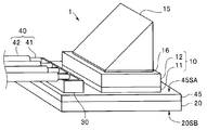
- the semiconductor device of the present embodiment shown in FIGS. 1, 2 and 3 is the image pickup device 1 arranged at the tip 90A of the endoscope 9 (see FIG. 19).
- the horizontal type image pickup device 1 includes an image pickup section 10 which is a semiconductor section, a prism 15, a wiring layer 20, a terminal section 30, an electric cable 40, and a resin layer 45.
- the image pickup unit 10 includes an image pickup element 11 which is a semiconductor element and a cover glass 12.
- the imaging unit 10 is a rectangular parallelepiped having a first surface 10SA and a second surface 10SB facing the first surface 10SA.
- a plurality of external electrodes 14 are arranged on the second surface 10SB.
- the light receiving portion 13 of the image sensor 11 and the external electrode 14 are connected to each other, for example, via the first penetrating wiring 11X (see FIG. 5).
- the image sensor 11 may be either a front side illumination type image sensor or a back side illumination type image sensor.
- the prism 15 is adhered to the first surface 10SA with a transparent adhesive 16.
- the terminal portion 30 has a first upper surface 30SA1 and a lower surface 30SB that faces the first upper surface 30SA1.
- the terminal portion 30 is a cable connecting portion in which a plurality of core wire terminals (connection lands) 31 are arranged on the first upper surface 30SA1 and a plurality of core wire electrodes 32 are arranged on the lower surface 30SB.
- the core wire terminal 31 and the core wire electrode 32 are connected to each other, for example, via the second through wiring 30X (see FIG. 5).
- the wiring layer 20 is a wiring member having a third surface 20SA and a fourth surface 20SB facing the third surface 20SA, and including an insulating layer 22 (22A, 22B) and a wiring 21.
- the third surface 20SA is in contact with the second surface 10SB of the imaging unit 10 and the lower surface 30SB of the terminal unit 30.
- the electric cable 40 has a core wire 41 and a first coating layer 42 that covers the core wire 41.
- the core wire 41 is joined to the core wire terminal 31 of the terminal portion 30 by using, for example, solder.
- the core wire 41 is electrically connected to the light receiving unit 13 via the core wire terminal 31, the second through wiring 30X, the core wire electrode 32, the wiring 21, and the external electrode 14.
- the resin layer 45 is arranged on the third surface 20SA of the wiring layer 20, and fixes the imaging unit 10 and the terminal unit 30.
- the resin layer 45 is a fixing portion that fixes the image pickup unit 10 and the terminal unit 30 to the wiring layer 20 in a state of being integrally held.
- the thickness H45 of the resin layer 45 is smaller than the thickness of the terminal portion 30 (the length H31 from the first upper surface 30SA1 to the lower surface 30SB). Therefore, the core terminal 31 of the terminal portion 30 is not covered with the resin layer 45. That is, the upper surface 45SA of the resin layer 45 is located at a position lower than the first surface 10SA and the first upper surface 30SA1 (position closer to the third surface 20SA).
- the upper surface 45SA of the resin layer 45 is parallel to the third surface 20SA of the wiring layer 20, and the outer dimensions of both are the same. In other words, the side surface of the resin layer 45 and the side surface of the wiring layer are on the same plane.
- the wiring 21 of the wiring layer 20 is in contact with the external electrode 14 and the core wire electrode 32.
- the wiring layer 20 is a rewiring layer provided on the resin layer 45 to which the imaging unit 10 and the terminal unit 30 are fixed.
- At least a region of the wiring 21 that is in contact with the external electrode 14 and the core wire electrode 32 is made of a conductive material deposited on the surfaces of the external electrode 14 and the core wire electrode 32.
- the wiring 21 is made of a copper sputtered film or a base conductive film and an electrolytic copper plating film formed on the external electrode 14 and the core wire electrode 32.
- the wiring 21 is formed into a film, and the wiring 21 and the external electrode 14 and the core wire electrode 32 are electrically connected to each other by being joined in a state of being in contact with each other. For this reason, the imaging device 1 is easy to manufacture and has high reliability in joining the wiring 21 to the external electrode 14 and the core wire electrode 32.
- the image pickup element When the electric cable 40 is joined to the external electrode 14 of the image pickup element 11, the image pickup element may be damaged by heat or stress at the time of joining. Further, when the image pickup device 11 is joined to the wiring board, the thickness of the image pickup device is increased.
- the external terminal 14 of the image pickup element 11 is in contact with the wiring 21 and is not joined using solder. Therefore, the image pickup element 11 is damaged by heat or stress when the solder is melted, and There is no risk of reducing reliability. Further, since the image pickup device 11 is fixed to the resin layer 45, not to the wiring board, the image pickup device 1 is thin and compact.
- a known semiconductor manufacturing technique is used to fabricate an imaging element wafer by disposing a plurality of light receiving sections 13 and the like on a silicon wafer. It Peripheral circuits that perform primary processing on the output signal of the light receiving unit 13 or process drive control signals may be formed on the imaging element wafer.
- a glass wafer that protects the light receiving section 13 is bonded to the light receiving surface of the image pickup element wafer. Then, the external electrode 14 connected to the light receiving portion 13 by passing through the first penetrating wiring 11X is arranged on the back surface.
- the image pickup element wafer to which the glass wafer is attached a plurality of image pickup sections 10 (image pickup element 11 to which the cover glass 12 is attached) are manufactured.
- the terminal portion 30 is a three-dimensional wiring board whose base is resin, ceramic, silicon or the like.
- the terminal portion 30 may be a molded circuit component (MID: Molded Interconnect Device) that is a three-dimensional component in which a conductive pattern is formed on an injection-molded product.
- MID Molded Interconnect Device
- the core wire terminal 31 and the core wire electrode 32 may be connected via a surface wiring.
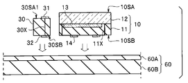
- Step S20 First Temporary Fixing Step As shown in FIG. 5, the imaging unit 10 and the terminal unit 30 are temporarily fixed to the first support substrate 60 in a predetermined arrangement state.
- an adhesive layer (temporary fixing layer) 60A is provided on a base body 60B. Since the adhesive layer 60A is soft, when the external electrode 14 and the core wire electrode 32 are convex electrodes, both are in a state of being embedded in the adhesive layer 60A. As will be described later, the adhesive layer 60A loses its adhesive force by ultraviolet irradiation treatment or heat treatment.
- the plurality of image capturing units 10 and the plurality of terminal units 30 are temporarily fixed to one first support substrate 60.
- the uncured resin layer 45 is disposed on the main surface 60SA around the image capturing section 10 and the terminal section 30 of the first support substrate 60.
- the resin layer 45 By curing the resin layer 45, the main part wafer 2W in which the imaging section 10 and the terminal section 30 are fixed by the resin layer 45 is manufactured.
- the uncured epoxy resin is disposed on the first support substrate 60, and then the thermosetting process is performed.
- the resin layer 45 is arranged so as not to cover the first surface 10SA of the imaging unit 10 and the first upper surface 30SA1 of the terminal unit 30.
- the resin layer 45 may completely cover the side surface of the imaging unit 10.
- the main wafer 2W in which the plurality of imaging units 10 and the plurality of terminal units 30 are fixed by the resin layer 45 is separated from the first support substrate 60.
- the adhesive layer 60A loses its adhesive force by the ultraviolet irradiation process, so that the main part wafer 2W is easily separated from the first support substrate 60.
- the lower surface 45SB of the resin layer 45, the second surface 10SB of the imaging unit 10, and the lower surface 30SB of the terminal portion 30 are located on the same plane.
- the external electrode 14 and the core wire electrode 32 are convex electrodes, both of them protrude from the plane including the lower surface 45SB of the resin layer 45.
- the external electrode 14 or the core wire electrode 32 is a convex electrode, only the convex electrode projects from the plane including the lower surface 45SB of the resin layer 45.
- the main wafer 2W is temporarily fixed to the second support substrate 61.
- the adhesive layer 61A is provided on the base 61B.
- the second support substrate 61 may have the same configuration as the first support substrate 60 or may have a different configuration.
- the first upper surface 30SA1 of the terminal portion 30 is temporarily fixed to the second support substrate 61. Further, when the terminal portion 30 has substantially the same height as the image pickup portion 10, the first upper surface 30SA1 of the terminal portion 30 and the first surface 10SA of the image pickup portion 10 are temporarily fixed to the second support substrate 61. . That is, at least one of the first surface 10SA and the first upper surface 30SA1 is temporarily fixed to the second support substrate 61.
- the wiring layer 20 including the wiring 21 that connects the external electrode 14 of the imaging unit 10 and the core wire electrode 32 of the terminal portion 30 and the insulating layer 22 (22A, 22B) is arranged.
- the wiring layer disposing step S60 includes a film forming step of forming the conductor layer 21M to be the wiring 21 on the respective surfaces of the external electrode 14 and the core wire electrode 32.
- the wiring 21 is formed into a film, the wiring 21 and the external electrode 14 and the core wire electrode 32 are brought into contact with each other without sandwiching other members, and are electrically connected. Therefore, the imaging device 1 is easy to manufacture, and the connection between the wiring 21 and the external electrode 14 and the core electrode 32 has a small electric resistance at the bonding interface and high reliability.
- an insulating layer 22A having an opening H22 exposing the external electrode 14 and an opening H23 exposing the core wire electrode 32 is provided. Side surfaces of the convex external electrode 14 and the core wire electrode 32 are covered with the insulating layer 22A.
- the external electrode 14 or the core wire electrode 32 is a convex electrode, only the side surface of the convex electrode is covered with the insulating layer 22A. That is, at least one of the side surface of the external electrode 14 and the side surface of the core wire electrode 32 is covered with the insulating layer 22A.
- the wiring 21 is formed by forming the wiring 21.
- the electrode 14 and the core wire electrode 32 can be regarded as an image pickup device in a contact state.
- the conductor layer 21M is formed in the openings H22, H23 and the insulating layer 22A.
- the conductor layer 21M is formed on the surface of the insulating layer 22A, the surface of the external electrode 14 exposed in the opening H22, and the surface of the core wire electrode 32 exposed in the opening H23 by sputtering or vapor deposition. To be done.
- the conductor layer 21M is made of copper or aluminum.
- the wiring 21 that connects the external electrode 14 and the core wire electrode 32 is produced by the patterning process of the conductor layer 21M.
- an electroplating method may be used after forming the underlying conductive film and using a plating mask in which the pattern of the wiring 21 is an opening.
- the electroplating method the underlying conductive film around the wiring 21 is removed after removing the plating mask.
- the wiring layer 20 is manufactured by disposing the insulating layer 22B that covers the wiring 21.
- the wiring layer 20 may be a multilayer wiring layer having two or more wirings 21.
- the main part wafer 2W including the wiring layer 20 is separated into the main parts 2. Since the main part 2 is produced by dividing (cutting) the main part wafer 2W, the side surface of the resin layer 45 and the side surface of the wiring layer 20 are cut surfaces cut at the same time, and the upper surface 45SA of the resin layer 45. And the third surface 20SA (fourth surface 20SB) of the wiring layer 20 have the same outer dimensions.
- the core wire 41 of the electric cable 40 is joined to the core wire terminal 31 of the terminal portion 30 of the main part 2.
- the prism 15 is adhered to the first main surface 10SA with an adhesive 16.
- the main wafer 2W to which the second support substrate 61 is bonded may be singulated, or before the singulated second support substrate 61 is separated.
- the electric cable 40 may be joined to the terminal portion 30. Furthermore, the electric cable 40 may be joined to the terminal portion 30 before the individual wafer 2W is singulated.
- the cutting step of dividing the main part wafer 2W into the main parts 2 is performed from after the wiring layer disposing step S60 to after the cable joining step S80.
- the imaging device 1 of the present embodiment is easy to manufacture because a large number of main parts 2 are manufactured in a wafer state.
- the main part 2 may be manufactured one by one.
- the image pickup unit 10A which is a semiconductor unit of the image pickup apparatus 1A, is an image pickup device having a thickness H10 in which the first surface 10SA is a light receiving surface.
- a cover glass or a prism may be adhered to the light receiving surface of the imaging unit 10A.
- the terminal portion 30A has a second upper surface 30SA2 that faces the lower surface 30SB and is parallel to the first upper surface 30SA1.
- the height H33 of the second upper surface 30SA2 from the lower surface 30SB is smaller than the height H31 of the first upper surface 30SA1.
- a shield terminal 33 is provided on the second upper surface 30SA2, and a shield electrode 34 is provided on the lower surface 30SB.
- the shield terminal 33 and the shield electrode 34 are connected by a through wiring or the like.
- the electric cable 40A is a shielded cable having a core wire 41, a first coating layer 42 that covers the core wire 41, a shield wire 43 that covers the first coating layer 42, and a second coating layer 44 that covers the shield wire 43.
- the core wire 41 is joined to the core wire terminal 31, and the shield wire 43 is joined to the shield terminal 33.
- the shield wires 43 of the plurality of electric cables 40A are joined to one shield terminal 33 which is a common terminal.
- the shield wires 43 of the plurality of electric cables 40A may be joined to the respective shield terminals 33.
- the length ⁇ 30 from the first upper surface 30SA1 to the second upper surface 30SA2 is the sum ⁇ 40 of the thickness T42 of the first coating layer 42 and the thickness T43 of the shield wire 43. Is substantially the same (for example, more than 75% and less than 125%). That is, the terminal portion 30A is set according to the electric cable 40A. Furthermore, in other words, the length ⁇ 30 from the first upper surface 30SA1 to the second upper surface 30SA2 is set to a distance at which the shield wire 43 also contacts the shield terminal 33 when the core wire 41 contacts the core terminal 31. ing.
- the core wire 41 and the shield wire 43 of the electric cable 40A which is a shielded cable, can be easily joined to the terminal portion 30A.
- the imaging device 1B and the method of manufacturing the imaging device 1B according to the present embodiment are similar to the imaging device 1 and the manufacturing method of the imaging device 1 and have the same effect, the same reference numeral is given to the component having the same function and described. Is omitted.
- the image pickup section 10B in which the cover glass 12B is bonded to the light receiving surface 11SA of the image pickup element 11B orthogonal to the second surface 10SB is a semiconductor section. That is, the imaging unit 10B is arranged such that the direction of the optical axis O of the imaging element 11B is parallel to the third surface 20SA of the wiring layer 20.
- the first surface 10SA and the second surface 10SB are side surfaces of the image pickup device 11B having a smaller area than the light receiving surface 11SA.
- facing surface 11SB facing the light receiving surface 11SA of the imaging unit 10B may be in contact with the side surface of the terminal unit 30 in order to facilitate the positioning between the terminal unit 30 and the imaging unit 10B.
- the image pickup apparatus 1B is a vertical type image pickup apparatus that does not include a prism, but has the same effect as the horizontal type image pickup apparatus 1 and the like. Further, the vertically-placed image pickup device 1B is shorter and smaller than the horizontally-placed image pickup device 1.
- the semiconductor device 1C and the method of manufacturing the semiconductor device 1C according to the present embodiment are similar to the imaging device 1 and the method of manufacturing the imaging device 1 and have the same effect, and therefore, components having the same function are denoted by the same reference numerals and described. Is omitted.
- a semiconductor device 1C shown in FIG. 18 has a semiconductor section 10C.
- the semiconductor unit 10 processes signals input/output by passing through the terminal 42.
- an AD conversion circuit for example, an AD conversion circuit, a memory, a transmission output circuit, a filter circuit, a thin film capacitor, a thin film resistor, a thin film, which performs primary processing on an image pickup signal output from an image pickup device (not shown) and processes a control signal for controlling the image pickup device. It is an inductor.
- the semiconductor device 1C has high reliability because the wiring 21 is formed on the surface of the external electrode 14 of the semiconductor unit 10 and heat and stress are not applied to the semiconductor unit 10. Moreover, since the main part 2 to which the electric cable 40 is joined is manufactured by the wafer process, the manufacturing is easy.
- the semiconductor device having the semiconductor section is not limited to the image pickup apparatus having the image pickup section.
- various semiconductor devices including an AD conversion circuit for an operation signal in the operation unit 91, a memory, a transmission output circuit, a filter circuit, a thin film capacitor, a thin film resistor, and a terminal unit to which an electric cable of a thin film inductor is joined.
- An endoscope system 8 including the endoscope 9 of the present embodiment shown in FIG. 19 includes the endoscope 9, a processor 80, a light source device 81, and a monitor 82.
- the endoscope 9 has an insertion section 90, an operation section 91, and a universal cord 92, and the imaging signal output from the imaging device 1 or the like arranged at the distal end portion 90A of the insertion section 90 is inserted into the insertion section 90. It is transmitted by the electric cable 40.
- the universal cord 92 extending from the operation unit 91 is connected to the processor 80 and the light source device 81 via the connector 93.
- the endoscope 9 has the insertion portion 90 inserted into the body cavity of the subject, captures an in-vivo image of the subject, and outputs an image signal.
- the insertion portion 90 is provided continuously with the distal end portion 90A in which the imaging device 1 is arranged, the bendable bending portion 90B continuously provided at the proximal end portion of the distal end portion 90A, and the proximal end portion of the bending portion 90B. And a flexible portion 90C.
- the bending section 90B is bent by the operation of the operation section 91.
- the endoscope 9 may be a rigid endoscope, and its application may be medical or industrial.
- an operation portion 91 provided with various buttons for operating the endoscope 9 is arranged.
- the light source device 81 has, for example, a white LED.
- the illumination light emitted from the light source device 81 passes through the universal cord 92 and a light guide (not shown) that passes through the insertion portion 90 and is guided to the tip 90A to illuminate the subject.
- the imaging device 1 is highly reliable and small, and therefore the endoscope 9 is highly reliable and has a small diameter.
- the endoscopes 9A to 9C equipped with the imaging devices 1A, 1B or the semiconductor device 1C have the effects of the imaging devices 1A, 1B or the semiconductor device 1C in addition to the effects of the endoscope 9. There is also no.
- Imaging part (semiconductor part) 10SA... First surface 10SB... Second surface 11... Imaging element 11B... Imaging element 11SA... Light receiving surface 11SB... Opposing surface 12... Cover glass 13... Light receiving part 14... External electrode 15... Prism 20... Wiring layer 20SA... Third surface 20SB... Fourth surface 21... Wiring 21M... Conductor layer 22A... Insulating layer 22A 22B... Insulating layer 30... Terminal part 30SA1... 1st upper surface 30SA2... 2nd upper surface 30SB... Lower surface 31... Core wire terminal 32... Core wire electrode 33... Shield Terminal 34... Shield electrode 40... Electric cable 41...
- Core wire 42 First coating layer 43... Shield wire 44... Second coating layer 45... Resin layer 45SA... Upper surface 45SB... Lower surface 60... First support substrate 60A... Adhesive layer 60B... Substrate 61... Second support substrate 61A... Adhesive layer 61B... Substrate
Landscapes
- Health & Medical Sciences (AREA)
- Life Sciences & Earth Sciences (AREA)
- Engineering & Computer Science (AREA)
- Surgery (AREA)
- Multimedia (AREA)
- Signal Processing (AREA)
- Radiology & Medical Imaging (AREA)
- Molecular Biology (AREA)
- Optics & Photonics (AREA)
- Pathology (AREA)
- Biophysics (AREA)
- Physics & Mathematics (AREA)
- Biomedical Technology (AREA)
- Heart & Thoracic Surgery (AREA)
- Medical Informatics (AREA)
- Nuclear Medicine, Radiotherapy & Molecular Imaging (AREA)
- Animal Behavior & Ethology (AREA)
- General Health & Medical Sciences (AREA)
- Public Health (AREA)
- Veterinary Medicine (AREA)
- Manufacturing & Machinery (AREA)
- Endoscopes (AREA)
- Solid State Image Pick-Up Elements (AREA)
Abstract
Un dispositif d'imagerie (1) comprend : une unité d'imagerie (10) qui présente une première surface (10SA) et une seconde surface (10SB), la seconde surface (10SB) étant pourvue d'une électrode externe (14); une partie borne (30) pourvue d'une borne de fil centrale (31) disposée sur une première surface supérieure (30SA1) de celle-ci et dotée d'une électrode filaire centrale (32) disposée sur une surface inférieure (30SB) de celle-ci; une couche de câblage (20) qui comprend une couche isolante (22) et un fil (21) et qui présente une troisième surface (20SA) en butée sur la deuxième surface (10SB) et la surface inférieure (30SB); une couche de résine (45) qui est disposée sur la troisième surface (20SA) et dont les dimensions extérieures sont identiques à celles de la couche de câblage (20), et qui fixe l'unité d'imagerie (10) et la partie borne (30) sans recouvrir la première surface (10SA) et la première surface supérieure (30SA1); et un câble électrique (40) pourvu d'un fil central (41) relié à la borne filaire centrale (31). Le fil (21) vient en butée contre l'électrode externe (14) et l'électrode filaire centrale (32).
Priority Applications (2)
| Application Number | Priority Date | Filing Date | Title |
|---|---|---|---|
| PCT/JP2018/044530 WO2020115813A1 (fr) | 2018-12-04 | 2018-12-04 | Dispositif à semiconducteur, endoscope, et procédé de fabrication de dispositif à semiconducteur |
| US17/336,499 US12033975B2 (en) | 2018-12-04 | 2021-06-02 | Semiconductor device, endoscope, and method for manufacturing semiconductor device |
Applications Claiming Priority (1)
| Application Number | Priority Date | Filing Date | Title |
|---|---|---|---|
| PCT/JP2018/044530 WO2020115813A1 (fr) | 2018-12-04 | 2018-12-04 | Dispositif à semiconducteur, endoscope, et procédé de fabrication de dispositif à semiconducteur |
Related Child Applications (1)
| Application Number | Title | Priority Date | Filing Date |
|---|---|---|---|
| US17/336,499 Continuation US12033975B2 (en) | 2018-12-04 | 2021-06-02 | Semiconductor device, endoscope, and method for manufacturing semiconductor device |
Publications (1)
| Publication Number | Publication Date |
|---|---|
| WO2020115813A1 true WO2020115813A1 (fr) | 2020-06-11 |
Family
ID=70973852
Family Applications (1)
| Application Number | Title | Priority Date | Filing Date |
|---|---|---|---|
| PCT/JP2018/044530 Ceased WO2020115813A1 (fr) | 2018-12-04 | 2018-12-04 | Dispositif à semiconducteur, endoscope, et procédé de fabrication de dispositif à semiconducteur |
Country Status (2)
| Country | Link |
|---|---|
| US (1) | US12033975B2 (fr) |
| WO (1) | WO2020115813A1 (fr) |
Families Citing this family (1)
| Publication number | Priority date | Publication date | Assignee | Title |
|---|---|---|---|---|
| CN118973464A (zh) * | 2022-04-26 | 2024-11-15 | 奥林巴斯医疗株式会社 | 摄像单元和内窥镜 |
Citations (6)
| Publication number | Priority date | Publication date | Assignee | Title |
|---|---|---|---|---|
| JP2001016486A (ja) * | 1999-06-25 | 2001-01-19 | Toshiba Corp | 固体撮像素子モジュール |
| JP2005317887A (ja) * | 2004-04-28 | 2005-11-10 | Advanced Chip Engineering Technology Inc | イメージセンサモジュールの構造及びウェハレベルパッケージを製造する方法 |
| JP2013215309A (ja) * | 2012-04-05 | 2013-10-24 | Olympus Corp | 内視鏡 |
| JP2014164110A (ja) * | 2013-02-25 | 2014-09-08 | Rohm Co Ltd | 光通信モジュールおよびその製造方法 |
| WO2017037828A1 (fr) * | 2015-08-31 | 2017-03-09 | オリンパス株式会社 | Endoscope, unité électronique, et procédé de fabrication d'une unité électronique |
| WO2018186163A1 (fr) * | 2017-04-06 | 2018-10-11 | オリンパス株式会社 | Unité d'imagerie et endoscope |
Family Cites Families (6)
| Publication number | Priority date | Publication date | Assignee | Title |
|---|---|---|---|---|
| JP4865267B2 (ja) * | 2005-07-14 | 2012-02-01 | 富士フイルム株式会社 | 固体撮像装置及び内視鏡 |
| JP2007287801A (ja) | 2006-04-13 | 2007-11-01 | Sony Corp | 電気・光混載三次元半導体モジュール及びハイブリット回路装置並びに携帯型電話機 |
| JP5302138B2 (ja) | 2009-08-31 | 2013-10-02 | オリンパスメディカルシステムズ株式会社 | 撮像装置及び電子内視鏡 |
| CN107210306B (zh) * | 2015-01-23 | 2020-07-14 | 奥林巴斯株式会社 | 摄像装置和内窥镜 |
| KR101982040B1 (ko) | 2016-06-21 | 2019-05-24 | 삼성전기주식회사 | 팬-아웃 반도체 패키지 |
| JP6393018B1 (ja) | 2017-04-06 | 2018-09-19 | オリンパス株式会社 | 撮像ユニット、および内視鏡 |
-
2018
- 2018-12-04 WO PCT/JP2018/044530 patent/WO2020115813A1/fr not_active Ceased
-
2021
- 2021-06-02 US US17/336,499 patent/US12033975B2/en active Active
Patent Citations (6)
| Publication number | Priority date | Publication date | Assignee | Title |
|---|---|---|---|---|
| JP2001016486A (ja) * | 1999-06-25 | 2001-01-19 | Toshiba Corp | 固体撮像素子モジュール |
| JP2005317887A (ja) * | 2004-04-28 | 2005-11-10 | Advanced Chip Engineering Technology Inc | イメージセンサモジュールの構造及びウェハレベルパッケージを製造する方法 |
| JP2013215309A (ja) * | 2012-04-05 | 2013-10-24 | Olympus Corp | 内視鏡 |
| JP2014164110A (ja) * | 2013-02-25 | 2014-09-08 | Rohm Co Ltd | 光通信モジュールおよびその製造方法 |
| WO2017037828A1 (fr) * | 2015-08-31 | 2017-03-09 | オリンパス株式会社 | Endoscope, unité électronique, et procédé de fabrication d'une unité électronique |
| WO2018186163A1 (fr) * | 2017-04-06 | 2018-10-11 | オリンパス株式会社 | Unité d'imagerie et endoscope |
Also Published As
| Publication number | Publication date |
|---|---|
| US20210288023A1 (en) | 2021-09-16 |
| US12033975B2 (en) | 2024-07-09 |
Similar Documents
| Publication | Publication Date | Title |
|---|---|---|
| US20180070799A1 (en) | Imaging device, endoscope system, and method of manufacturing imaging device | |
| JP5926890B2 (ja) | 配線板、配線板の製造方法、および撮像装置 | |
| US9509890B2 (en) | Solid image pickup apparatus | |
| US10930696B2 (en) | Image pickup unit, endoscope, and method for manufacturing image pickup unit | |
| US11000184B2 (en) | Image pickup module, fabrication method for image pickup module, and endoscope | |
| WO2015045616A1 (fr) | Unité d'imagerie et dispositif d'endoscope | |
| WO2018092318A1 (fr) | Module d'imagerie endoscopique et endoscope | |
| WO2018173261A1 (fr) | Endoscope et module composite photoélectrique | |
| US20200059576A1 (en) | Endoscope, image pickup apparatus and endoscope manufacturing method | |
| US20230291988A1 (en) | Image pickup unit, method of manufacturing image pickup unit, and endoscope | |
| JP2011045173A (ja) | 集合ケーブル、電子回路モジュールおよび撮像装置 | |
| WO2018092234A1 (fr) | Module optique,capture d'image et endoscope | |
| CN106455952A (zh) | 摄像单元、带缆线的配线板以及带缆线的配线板的制造方法 | |
| WO2020115813A1 (fr) | Dispositif à semiconducteur, endoscope, et procédé de fabrication de dispositif à semiconducteur | |
| CN104902802B (zh) | 内窥镜用摄像单元 | |
| WO2016208043A1 (fr) | Carte de circuit électronique, carte stratifiée et procédé de fabrication de carte de circuit électronique | |
| JP6081170B2 (ja) | 撮像装置、内視鏡及び撮像装置の製造方法 | |
| US20210250473A1 (en) | Image pickup apparatus, endoscope and method for manufacturing image pickup apparatus | |
| JP7702341B2 (ja) | 内視鏡撮像装置及び内視鏡 | |
| US11287641B2 (en) | Image pickup apparatus, endoscope, and method for manufacturing image pickup apparatus | |
| US10888217B2 (en) | Imaging module applicable to head-swing endoscope | |
| WO2021260863A1 (fr) | Module électronique, procédé de fabrication de module électronique et endoscope | |
| US11876107B2 (en) | Image pickup apparatus for endoscope and endoscope | |
| JP7149489B2 (ja) | 固体撮像装置 | |
| WO2021149177A1 (fr) | Dispositif d'imagerie, endoscope et procédé de fabrication de dispositif d'imagerie |
Legal Events
| Date | Code | Title | Description |
|---|---|---|---|
| 121 | Ep: the epo has been informed by wipo that ep was designated in this application |
Ref document number: 18942006 Country of ref document: EP Kind code of ref document: A1 |
|
| NENP | Non-entry into the national phase |
Ref country code: DE |
|
| 122 | Ep: pct application non-entry in european phase |
Ref document number: 18942006 Country of ref document: EP Kind code of ref document: A1 |
|
| NENP | Non-entry into the national phase |
Ref country code: JP |