WO2020121697A1 - Procédé de formation de nanopores et procédé d'analyse - Google Patents
Procédé de formation de nanopores et procédé d'analyse Download PDFInfo
- Publication number
- WO2020121697A1 WO2020121697A1 PCT/JP2019/043577 JP2019043577W WO2020121697A1 WO 2020121697 A1 WO2020121697 A1 WO 2020121697A1 JP 2019043577 W JP2019043577 W JP 2019043577W WO 2020121697 A1 WO2020121697 A1 WO 2020121697A1
- Authority
- WO
- WIPO (PCT)
- Prior art keywords
- aqueous solution
- electrode
- nanopore
- sinx
- membrane
- Prior art date
- Legal status (The legal status is an assumption and is not a legal conclusion. Google has not performed a legal analysis and makes no representation as to the accuracy of the status listed.)
- Ceased
Links
Images



Classifications
-
- B—PERFORMING OPERATIONS; TRANSPORTING
- B81—MICROSTRUCTURAL TECHNOLOGY
- B81C—PROCESSES OR APPARATUS SPECIALLY ADAPTED FOR THE MANUFACTURE OR TREATMENT OF MICROSTRUCTURAL DEVICES OR SYSTEMS
- B81C1/00—Manufacture or treatment of devices or systems in or on a substrate
- B81C1/00015—Manufacture or treatment of devices or systems in or on a substrate for manufacturing microsystems
- B81C1/00023—Manufacture or treatment of devices or systems in or on a substrate for manufacturing microsystems without movable or flexible elements
- B81C1/00087—Holes
-
- B—PERFORMING OPERATIONS; TRANSPORTING
- B01—PHYSICAL OR CHEMICAL PROCESSES OR APPARATUS IN GENERAL
- B01J—CHEMICAL OR PHYSICAL PROCESSES, e.g. CATALYSIS OR COLLOID CHEMISTRY; THEIR RELEVANT APPARATUS
- B01J19/00—Chemical, physical or physico-chemical processes in general; Their relevant apparatus
- B01J19/08—Processes employing the direct application of electric or wave energy, or particle radiation; Apparatus therefor
-
- B—PERFORMING OPERATIONS; TRANSPORTING
- B81—MICROSTRUCTURAL TECHNOLOGY
- B81B—MICROSTRUCTURAL DEVICES OR SYSTEMS, e.g. MICROMECHANICAL DEVICES
- B81B1/00—Devices without movable or flexible elements, e.g. microcapillary devices
- B81B1/002—Holes characterised by their shape, in either longitudinal or sectional plane
- B81B1/004—Through-holes, i.e. extending from one face to the other face of the wafer
-
- B—PERFORMING OPERATIONS; TRANSPORTING
- B82—NANOTECHNOLOGY
- B82Y—SPECIFIC USES OR APPLICATIONS OF NANOSTRUCTURES; MEASUREMENT OR ANALYSIS OF NANOSTRUCTURES; MANUFACTURE OR TREATMENT OF NANOSTRUCTURES
- B82Y35/00—Methods or apparatus for measurement or analysis of nanostructures
-
- B—PERFORMING OPERATIONS; TRANSPORTING
- B82—NANOTECHNOLOGY
- B82Y—SPECIFIC USES OR APPLICATIONS OF NANOSTRUCTURES; MEASUREMENT OR ANALYSIS OF NANOSTRUCTURES; MANUFACTURE OR TREATMENT OF NANOSTRUCTURES
- B82Y40/00—Manufacture or treatment of nanostructures
-
- G—PHYSICS
- G01—MEASURING; TESTING
- G01N—INVESTIGATING OR ANALYSING MATERIALS BY DETERMINING THEIR CHEMICAL OR PHYSICAL PROPERTIES
- G01N27/00—Investigating or analysing materials by the use of electric, electrochemical, or magnetic means
- G01N27/002—Investigating or analysing materials by the use of electric, electrochemical, or magnetic means by investigating the work function voltage
-
- G—PHYSICS
- G01—MEASURING; TESTING
- G01N—INVESTIGATING OR ANALYSING MATERIALS BY DETERMINING THEIR CHEMICAL OR PHYSICAL PROPERTIES
- G01N33/00—Investigating or analysing materials by specific methods not covered by groups G01N1/00 - G01N31/00
- G01N33/48—Biological material, e.g. blood, urine; Haemocytometers
- G01N33/483—Physical analysis of biological material
- G01N33/487—Physical analysis of biological material of liquid biological material
- G01N33/48707—Physical analysis of biological material of liquid biological material by electrical means
- G01N33/48721—Investigating individual macromolecules, e.g. by translocation through nanopores
-
- H—ELECTRICITY
- H10—SEMICONDUCTOR DEVICES; ELECTRIC SOLID-STATE DEVICES NOT OTHERWISE PROVIDED FOR
- H10P—GENERIC PROCESSES OR APPARATUS FOR THE MANUFACTURE OR TREATMENT OF DEVICES COVERED BY CLASS H10
- H10P50/00—Etching of wafers, substrates or parts of devices
-
- B—PERFORMING OPERATIONS; TRANSPORTING
- B81—MICROSTRUCTURAL TECHNOLOGY
- B81B—MICROSTRUCTURAL DEVICES OR SYSTEMS, e.g. MICROMECHANICAL DEVICES
- B81B2201/00—Specific applications of microelectromechanical systems
- B81B2201/02—Sensors
- B81B2201/0214—Biosensors; Chemical sensors
-
- B—PERFORMING OPERATIONS; TRANSPORTING
- B81—MICROSTRUCTURAL TECHNOLOGY
- B81C—PROCESSES OR APPARATUS SPECIALLY ADAPTED FOR THE MANUFACTURE OR TREATMENT OF MICROSTRUCTURAL DEVICES OR SYSTEMS
- B81C2201/00—Manufacture or treatment of microstructural devices or systems
- B81C2201/01—Manufacture or treatment of microstructural devices or systems in or on a substrate
- B81C2201/0101—Shaping material; Structuring the bulk substrate or layers on the substrate; Film patterning
- B81C2201/0128—Processes for removing material
- B81C2201/013—Etching
- B81C2201/0133—Wet etching
-
- B—PERFORMING OPERATIONS; TRANSPORTING
- B81—MICROSTRUCTURAL TECHNOLOGY
- B81C—PROCESSES OR APPARATUS SPECIALLY ADAPTED FOR THE MANUFACTURE OR TREATMENT OF MICROSTRUCTURAL DEVICES OR SYSTEMS
- B81C2201/00—Manufacture or treatment of microstructural devices or systems
- B81C2201/01—Manufacture or treatment of microstructural devices or systems in or on a substrate
- B81C2201/0101—Shaping material; Structuring the bulk substrate or layers on the substrate; Film patterning
- B81C2201/0128—Processes for removing material
- B81C2201/0146—Processes for removing material not provided for in B81C2201/0129 - B81C2201/0145
-
- B—PERFORMING OPERATIONS; TRANSPORTING
- B82—NANOTECHNOLOGY
- B82Y—SPECIFIC USES OR APPLICATIONS OF NANOSTRUCTURES; MEASUREMENT OR ANALYSIS OF NANOSTRUCTURES; MANUFACTURE OR TREATMENT OF NANOSTRUCTURES
- B82Y30/00—Nanotechnology for materials or surface science, e.g. nanocomposites
-
- C—CHEMISTRY; METALLURGY
- C12—BIOCHEMISTRY; BEER; SPIRITS; WINE; VINEGAR; MICROBIOLOGY; ENZYMOLOGY; MUTATION OR GENETIC ENGINEERING
- C12M—APPARATUS FOR ENZYMOLOGY OR MICROBIOLOGY; APPARATUS FOR CULTURING MICROORGANISMS FOR PRODUCING BIOMASS, FOR GROWING CELLS OR FOR OBTAINING FERMENTATION OR METABOLIC PRODUCTS, i.e. BIOREACTORS OR FERMENTERS
- C12M1/00—Apparatus for enzymology or microbiology
-
- C—CHEMISTRY; METALLURGY
- C12—BIOCHEMISTRY; BEER; SPIRITS; WINE; VINEGAR; MICROBIOLOGY; ENZYMOLOGY; MUTATION OR GENETIC ENGINEERING
- C12M—APPARATUS FOR ENZYMOLOGY OR MICROBIOLOGY; APPARATUS FOR CULTURING MICROORGANISMS FOR PRODUCING BIOMASS, FOR GROWING CELLS OR FOR OBTAINING FERMENTATION OR METABOLIC PRODUCTS, i.e. BIOREACTORS OR FERMENTERS
- C12M1/00—Apparatus for enzymology or microbiology
- C12M1/34—Measuring or testing with condition measuring or sensing means, e.g. colony counters
-
- C—CHEMISTRY; METALLURGY
- C12—BIOCHEMISTRY; BEER; SPIRITS; WINE; VINEGAR; MICROBIOLOGY; ENZYMOLOGY; MUTATION OR GENETIC ENGINEERING
- C12Q—MEASURING OR TESTING PROCESSES INVOLVING ENZYMES, NUCLEIC ACIDS OR MICROORGANISMS; COMPOSITIONS OR TEST PAPERS THEREFOR; PROCESSES OF PREPARING SUCH COMPOSITIONS; CONDITION-RESPONSIVE CONTROL IN MICROBIOLOGICAL OR ENZYMOLOGICAL PROCESSES
- C12Q1/00—Measuring or testing processes involving enzymes, nucleic acids or microorganisms; Compositions therefor; Processes of preparing such compositions
- C12Q1/68—Measuring or testing processes involving enzymes, nucleic acids or microorganisms; Compositions therefor; Processes of preparing such compositions involving nucleic acids
- C12Q1/6869—Methods for sequencing
Definitions
- the present disclosure relates to a nanopore formation method and an analysis method.
- the nanopore device is equipped with holes (nanopores) of the same size as the molecules and particles to be detected in the membrane, fill the chambers above and below the membrane with aqueous solution, and contact the aqueous solution in both chambers. It is provided with electrodes.
- the detection target is introduced into one side of the chamber, passed through the nanopores by applying a potential difference between the electrodes and electrophoresed, and the time change of the ionic current (blocking signal) flowing between both electrodes is measured to detect the detection target. It is possible to detect the passage of an object and analyze the structural characteristics of the detection target.
- Non-Patent Document 1 a silicon nitride film (SiNx film) is used as a membrane, and a TEM (transmission electron microscope) device is used to reduce the irradiation area of an electron beam to a small area on the membrane. It is disclosed that nanopores having a diameter of 10 nm or less are formed by controlling energy and current.
- Patent Document 1 and Non-Patent Documents 2 to 4 disclose nanopore forming methods utilizing dielectric breakdown of a membrane.
- the upper and lower chambers sandwiching a non-perforated SiNx membrane are filled with an aqueous solution, the electrodes are immersed in the aqueous solution of each chamber, and a high voltage is continuously applied between both electrodes.
- the current value between the electrodes suddenly rises (dielectric breakdown of the membrane) and the preset cut-off current value is reached, it is judged that the nanopores are formed, and by stopping the application of high voltage, the nanopores are stopped. To form.
- the present nanopore forming method has an advantage that the manufacturing cost is significantly reduced and the throughput is improved as compared with the nanopore forming using the TEM device.
- the present nanopore formation method can shift to measurement of a detection target without removing the membrane from the chamber after forming the nanopore in the membrane. Therefore, there is an advantage that the nanopore is not exposed to pollutants in the air and noise during measurement is reduced.
- An application of measurement using nanopores is decoding the base sequence of DNA (DNA sequencing). That is, it is a method of determining the sequence of four types of bases in a DNA chain by detecting a change in ionic current when DNA passes through a nanopore.
- Non-Patent Document 5 Another application of measurement using nanopores is detection and counting of specific objects in aqueous solution.
- PNA and PEG are bound only to DNA having a specific sequence present in an aqueous solution, and a change in ionic current when DNA modified with PNA and PEG passes through a nanopore is measured.
- the dielectric breakdown voltage the breakdown voltage against the voltage applied to the membrane
- the dielectric breakdown voltage it is desirable to use a membrane that is unlikely to cause dielectric breakdown even if a voltage required for measurement is applied for a long time.
- a high voltage is applied to the membrane due to static electricity generated during setup before measurement, and the membrane causes dielectric breakdown (Non-Patent Document 6).
- the dielectric breakdown voltage is high. Therefore, a membrane that is resistant to dielectric breakdown even when a high voltage is applied is desirable.
- Non-Patent Documents 2 to 4 attempts to form nanopores using dielectric breakdown for a SiNx membrane (1 ⁇ x ⁇ 4/3) having a high dielectric breakdown voltage, a single nanopore is formed. I found it difficult to do.
- the present disclosure provides a technique for stably forming a single nanopore on a membrane having a high dielectric breakdown voltage by dielectric breakdown.
- the nanopore formation method of this indication arrange
- a single nanopore can be stably formed on a membrane having a high dielectric breakdown voltage by dielectric breakdown.
- FIG. 1 It is a schematic diagram which shows the apparatus structure for the nanopore formation method which concerns on 1st Embodiment. It is a figure which shows the result of the comparative example 1. It is a figure which shows the result of the comparative example 2. It is a figure which shows the result of the comparative example 3. It is a figure which shows the result of the comparative example 4. 5 is a diagram showing the results of Example 1.
- FIG. It is a figure which shows the result of Experimental example 2.
- FIG. 1A is a schematic diagram showing the configuration of an apparatus for the method for forming nanopores according to the first embodiment.
- the apparatus for the nanopore forming method includes a Si substrate 100, a SiNx film 101, a SiO 2 film 102, a SiNx film 103, an O-ring 104, a first chamber 105, and a second chamber.
- the Si substrate 100, the SiNx film 101, the SiO 2 film 102, and the SiNx film 103 are arranged in this order.
- An O-ring 104 is arranged on each of the upper surface of the SiNx film 103 and the lower surface of the Si substrate 100, and the O-ring 104 closes the first chamber 105 and the second chamber 106.
- the SiNx film 101 has a SiNx membrane 113 (film) as shown in the dotted frame of FIG.
- the SiNx membrane 113 is where the nanopores are formed, the Si substrate 100 and the SiO 2 film 102 do not exist above and below the SiNx membrane 113, and the upper and lower surfaces are in contact with the first aqueous solution 107 and the second aqueous solution 108, respectively.
- the SiO 2 film 102 and the SiNx film 103 are for adjusting the region (size) of the SiNx membrane 113 and are not essential. That is, the SiO 2 film 102 and the SiNx film 103 may or may not be provided.
- the Si substrate 100 also exists as a member that supports the SiNx film 101 and the SiNx membrane 113. Therefore, the Si substrate 100 may be a member made of another material other than Si.
- FIG. 1B is a schematic view showing another configuration of the apparatus for the nanopore forming method.
- the Si substrate 100 is not used, and the SiO 2 film 102 and the SiNx film 103 are not arranged, and the SiNx film 101 is directly attached to the first chamber 105 and the second chamber 106. It may be set up. That is, it suffices that the upper and lower first aqueous solution 107 and second aqueous solution 108 are separated via the target SiNx membrane 113.
- the composition ratio x of the SiNx membrane 113 is 1 ⁇ x ⁇ 4/3.
- the composition ratio x is an average value of a plurality of values measured in the thickness direction from the front surface or the back surface of the film by X-ray photoelectron spectroscopy (XPS) analysis or secondary ion mass spectrometry (SIMS).
- XPS X-ray photoelectron spectroscopy
- SIMS secondary ion mass spectrometry
- SiNx membrane 113 only a part of the SiNx film 101 is referred to as a SiNx membrane 113, and the SiNx film 101 and the SiNx membrane 113 are formed in the same film forming process. It is a single film made of the same member as described above. Therefore, in the SiNx film 101, the composition ratio x of the region other than the SiNx membrane 113 part is the same as the composition ratio x of the SiNx membrane 113 part.
- the SiO 2 film 102 and the SiNx film 103 on the Si substrate 100 are removed by etching, and the SiNx film 101 on the Si substrate 100 is removed.
- XPS measurement is performed every time the SiNx film 101 is etched from the surface in the depth direction, whereby the composition ratio x at each depth in the film can be measured. Then, the measured composition ratio x may be considered as the composition ratio of the SiNx membrane 113.
- composition ratio x may be measured at any position on the SiNx film 101 in the horizontal direction.
- the measurement interval in the thickness direction (depth direction) of the SiNx film 101 can be set to 0.2 to 3 nm, for example.
- the first chamber 105 is provided with an aqueous solution introducing port 114 and an aqueous solution outlet 115, and the first aqueous solution 107 is introduced from the aqueous solution introducing port 114.
- An aqueous solution introducing port 116 and an aqueous solution outlet 117 are provided in the second chamber 106, and the second aqueous solution 108 is introduced from the aqueous solution introducing port 116. Details of the first aqueous solution 107 and the second aqueous solution 108 will be described later.
- the electrode 109 (first electrode) is arranged so as to contact the first aqueous solution 107 in the first chamber 105, and the electrode 110 (second electrode) is arranged in contact with the second aqueous solution 107 in the second chamber 106. It is placed in contact with the aqueous solution 108.
- the electrodes 109 and 110 are connected to the control unit 112 by the wiring 111.
- the electrodes 109 and 110 are, for example, silver/silver chloride electrodes.
- control unit 112 includes a power supply for applying a voltage to the electrodes 109 and 110 and an ammeter for measuring the current between the electrodes 109 and 110, and controls these.
- the control unit 112 also performs control such that the voltage application is stopped when the current value between the electrodes 109 and 110 reaches a predetermined threshold current.
- control unit 112 includes an input unit for the user to set the threshold current, a storage unit for storing information input to the input unit, measurement results, etc., a display unit for displaying measurement conditions, measurement results, etc. May have.
- the method for forming nanopores according to the present embodiment is a method for forming nanopores by a dielectric breakdown method as in the methods described in Patent Document 1 and Non-Patent Documents 2 to 4 using the setup of FIG.
- the dielectric breakdown method is to measure a current flowing between the electrodes 109 and 110 while continuously applying a constant voltage to the electrodes 109 and 110, and the dielectric breakdown of the SiNx membrane 113 causes a rapid increase in the current value between the electrodes. It is a method of forming the nanopores in the SiNx membrane 113 by determining that the nanopores are formed when the preset threshold current is reached and stopping the application of the voltage.
- the SiNx membrane 113 is arranged between the first aqueous solution 107 and the second aqueous solution 108, the electrode 109 is brought into contact with the first aqueous solution 107, and the electrode 110 is removed. Contacting with the second aqueous solution 108 and applying a voltage to the electrodes 109 and 110.
- the pH of each of the first aqueous solution 107 and the second aqueous solution 108 is 10 or more.
- a KCl aqueous solution can be used as the first aqueous solution 107 and the second aqueous solution 108.
- a single nanopore can be formed by using an aqueous solution of LiCl, NaCl, CaCl 2 , MgCl 2 , CsCl or the like other than the KCl aqueous solution.
- the concentration of the first aqueous solution 107 and the second aqueous solution 108 may be, for example, 1M, but may be higher than 1M (for example, 1M or more and 3M or less) or less than 1M (for example, 0.001M or more). If the pH is 10 or more (when the film thickness of the SiNx membrane is 20 nm or more, it is higher than pH 11), a single nanopore can be formed.
- a SiNx membrane 113 having a thickness of 20 nm and a composition ratio x of 1 ⁇ x ⁇ 4/3 is used as the SiNx membrane 113, and the SiO 2 film 102 has a thickness of 250 nm and SiNx.
- the thickness of the film 103 was 100 nm.
- a 1M KCl aqueous solution adjusted to pH 7.5 was introduced as the first aqueous solution and the second aqueous solution, respectively.
- the predetermined threshold current is set to 0.3 ⁇ 10 ⁇ 6 A, and when the current value reaches 0.3 ⁇ 10 ⁇ 6 A, the control unit 112 is set to stop the application of the voltage to the electrodes 109 and 110. 0 V was applied to 109 and 20 V was applied to the electrode 110 to try to form nanopores.
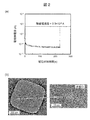
- FIG. 2A is a graph showing the interelectrode current value (A) when voltage is applied in Comparative Example 1. As shown in FIG. 2( a ), when the voltage application time was about 230 s, the inter-electrode current value drastically increased and reached 0.3 ⁇ 10 ⁇ 6 A.
- FIG. 2B is a TEM photograph of the SiNx membrane after the dielectric breakdown in Comparative Example 1.
- the left side of FIG. 2B is a photograph of the entire view of the SiNx membrane seen from above.
- the TEM photographs of FIG. 2 and the like show that the lighter the color, the thinner the film.
- a part of the SiNx membrane has a bright portion.
- An enlarged photograph of this portion is the photograph on the right side of FIG. From the photograph on the right side of FIG. 2B, it was found that no holes were formed and only a thin film region having a diameter of about 10 nm was formed.
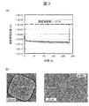
- Comparative Example 2 Comparative Example 2 was the same as Comparative Example 1 except that the predetermined threshold current was set to 1 ⁇ 10 ⁇ 6 A, with respect to the SiNx membrane (1 ⁇ x ⁇ 4/3), the nanopore by the dielectric breakdown method was used. Tried to form. Further, in the same manner as in Comparative Example 1, the current value when voltage was applied was measured, and the TEM observation of the SiNx membrane after dielectric breakdown was performed. Results are shown in FIG.
- FIG. 3A is a graph showing the current value when voltage is applied in Comparative Example 2. As shown in FIG. 3A, when the voltage application time was about 240 s, the inter-electrode current value rapidly increased and reached 1 ⁇ 10 ⁇ 6 A.
- FIG. 3B is a TEM photograph of the SiNx membrane after the dielectric breakdown in Comparative Example 2.
- a portion of the SiNx membrane has a bright color, as indicated by the arrow.
- An enlarged photograph of this portion is the photograph on the right side of FIG. From the photograph on the right side of FIG. 3B, it can be seen that a large thin film region is formed as compared with the case of FIG. 2B, but it was also found that no holes were formed. That is, it was found that when the pH 7.5 aqueous solution was used, nanopores were not formed even after the dielectric breakdown of the SiNx membrane.
- Comparative Example 3 was the same as Comparative Example 1 except that the threshold current was set to 3 ⁇ 10 ⁇ 6 A, and nanopores were formed on the SiNx membrane (1 ⁇ x ⁇ 4/3) by the dielectric breakdown method. Tried. Further, in the same manner as in Comparative Example 1, the current value when voltage was applied was measured, and the TEM observation of the SiNx membrane after dielectric breakdown was performed. The results are shown in Fig. 4.
- FIG. 4A is a graph showing the current value when voltage is applied in Comparative Example 3. As shown in FIG. 4A, when the voltage application time was about 270 s, the inter-electrode current value rapidly increased and reached 3 ⁇ 10 ⁇ 6 A.
- FIG. 4B is a TEM photograph of the SiNx membrane after the dielectric breakdown in Comparative Example 3.
- a part of the SiNx membrane has a bright color, as indicated by the arrow.
- An enlarged photograph of this portion is the photograph on the right side of FIG. From the photograph on the right side of FIG. 4B, it can be seen that a large thin film region is formed as compared with the case of FIG. 3B, but it was also found that no hole was formed. That is, it was found that when the pH 7.5 aqueous solution was used, nanopores were not formed even after the dielectric breakdown of the SiNx membrane.
- the threshold current is set to be smaller than 0.3 ⁇ 10 ⁇ 6 A, for example, 0.1 ⁇ 10 ⁇ 6 A or less, the nanopores are naturally formed. Was not done.
- Comparative example 4 In Comparative Example 4, formation of nanopores by a dielectric breakdown method was tried in the same manner as in Comparative Example 1 except that the threshold current was set to 6.5 ⁇ 10 ⁇ 6 A. Further, in the same manner as in Comparative Example 1, the current value when voltage was applied was measured, and the TEM observation of the SiNx membrane after dielectric breakdown was performed. Results are shown in FIG.
- FIG. 5A is a graph showing the current value when voltage is applied in Comparative Example 4. As shown in FIG. 5( a ), when the voltage application time was about 220 s, the interelectrode current value sharply increased and reached 6.5 ⁇ 10 ⁇ 6 A.
- FIG. 5B is a TEM photograph of the SiNx membrane after the dielectric breakdown in Comparative Example 4. In the photograph on the left side of FIG. 5B, it can be seen that a portion of the SiNx membrane has a bright color, as indicated by the arrow. An enlarged photograph of this portion is the photograph on the right side of FIG.
- the number of nanopores existing in the membrane be one. Another problem is that holes of various sizes are created. Because, if only holes smaller than the molecules or particles to be detected are created, the molecules or particles to be detected cannot pass through the holes, and as a result, it is impossible to detect or count the molecules or particles to be detected. Because.
- Comparative Examples 1 to 4 As shown in Comparative Examples 1 to 4 (FIGS. 2 to 5), when the threshold current value is set low, holes are not opened in the SiNx membrane, and when the threshold current value is set high, the holes are opened, but different sizes are set. It was found that a plurality of holes were formed. In addition, even if the threshold current value (3 ⁇ 10 ⁇ 6 A) of Comparative Example 3 and the threshold current value of Comparative Example 4 (6.5 ⁇ 10 ⁇ 6 A) were set to a threshold current value, an experiment was conducted. , The SiNx membrane has no holes or a plurality of holes having different sizes are formed. That is, it was found that it is not possible to form a single nanopore in the SiNx membrane simply by directly applying the methods described in Patent Document 1 and Non-Patent Documents 2 to 4.
- Patent Document 1 and Non-Patent Documents 2 to 4 show that a single nanopore can be formed on the SiNx membrane by the method of causing dielectric breakdown as described above.
- Non-Patent Document 2 by filling both sides of a SiNx membrane with a KCl aqueous solution having a pH of 10 and a concentration of 1M, applying a voltage to the SiNx membrane, and setting a threshold current value for stopping the voltage application to about 100 nA. , Forming a single nanopore with a diameter of about 3 nm. It is also described that a single nanopore can be formed on a SiNx membrane by the same method even when the pH is set to 2, 4, 7, 10 or 13.5.
- Non-Patent Document 3 by filling a KN aqueous solution having a pH of 8 and a concentration of 1 M on both sides of the SiNx membrane, applying a voltage to the SiNx membrane, and setting a threshold current value for stopping the voltage application to about 95 nA, It forms a single nanopore.
- Comparative Examples 1 to 4 we filled both sides of the SiNx membrane with an aqueous KCl solution having a pH of 7.5 and a concentration of 1M, applied a voltage to the SiNx membrane, and set a threshold current value for stopping the voltage application. Multiple values were investigated between about 100 nA or less and 10 ⁇ A, but it was impossible to form a single nanopore. Further, even if the pH of the 1 M KCl aqueous solution used was set to 7 or 8, the tendency of the above-mentioned experimental results did not change, and it was impossible to form a single nanopore.
- composition ratio x of the SiNx membrane is smaller than 1, as a result of attempting to form nanopores by the dielectric breakdown method, as the first aqueous solution 107 and the second aqueous solution 108, an aqueous solution having a pH of less than 10 was used. However, a single nanopore was formed.
- Example 1 a method of forming a single nanopore in a SiNx membrane (1 ⁇ x ⁇ 4/3) by a dielectric breakdown method will be described.
- the pH of the first aqueous solution 107 and the second aqueous solution 108 is 10 or more.
- Example 1 In Example 1, as in Comparative Example 1, using the setup of FIG. 1A, an attempt was made to form nanopores by a dielectric breakdown method on a SiNx membrane (1 ⁇ x ⁇ 4/3) having a thickness of 20 nm. It was
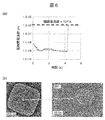
- FIG. 6A is a graph showing the current value when voltage is applied in the first embodiment. As shown in FIG. 6A, when the voltage application time was about 4 s, the interelectrode current value rapidly increased and reached 1 ⁇ 10 ⁇ 6 A.
- FIG. 6B is a TEM photograph of the SiNx membrane after dielectric breakdown in Example 1.
- the photograph on the left side of FIG. 6B is a photograph of the entire view of the SiNx membrane seen from above. As shown by the arrow in the photograph on the left side of FIG. 6B, it can be seen that a part of the SiNx membrane has a bright part. An enlarged photograph of this portion is the photograph on the right side of FIG. In the photograph on the right side of FIG. 6B, there was a portion where an amorphous pattern derived from SiNx could not be seen, and it was found that holes (nanopores) were opened. Further, from the photograph on the left side of FIG. 6B, it was found that only one hole was formed in the SiNx membrane.
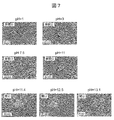
- the threshold current was set to 1 ⁇ 10 ⁇ 6 A, and the pH of the aqueous solution was changed in seven steps of 1, 3, 7.5, 11, 11.4, 12.5 and 13.1. Then, we tried to form nanopores by the dielectric breakdown method. The other conditions are the same as in Experimental Example 1 above.
- FIG. 7 is a TEM photograph of the SiNx membrane after dielectric breakdown when the pH of the aqueous solution was changed. As shown in FIG. 7, when the pH is higher than 11, it can be seen that there is a portion in which the amorphous pattern is not visible in the SiNx membrane and the nanopore is open. The number of nanopores formed was one for each SiNx membrane. On the other hand, it was found that when the pH was 11 or less, only the thin film region was formed in the SiNx membrane and the holes were not opened.
- Si is etched with a highly alkaline solution under high temperature. Therefore, when pores are formed in a SiNx membrane (1 ⁇ x ⁇ 4/3) by an insulation breakdown method in an aqueous solution having a pH of 10 or more, Si is temporarily more than N after insulation breakdown. A local thin film region composed of a very large proportion may be formed, but at the same time, etching of Si by an alkaline aqueous solution also occurs immediately, so that a hole is formed without leaving a local thin film region. To be done. Since SiNx (1 ⁇ x ⁇ 4/3) is not etched even in an alkaline aqueous solution, the entire membrane is not etched as a result, and holes can be locally formed. It should be noted that a high temperature is required to quickly etch Si with an alkaline solution, which is covered by Joule heat of a large current flowing after dielectric breakdown.
- the SiNx membrane particularly the membrane in which the composition ratio x is in the range of 1 ⁇ x ⁇ 4/3, has an excellent breakdown voltage (dielectric breakdown voltage) against an applied voltage.
- dielectric breakdown voltage is high because the object is measured while applying a voltage to the membrane.
- a membrane that is less susceptible to dielectric breakdown even if a voltage required for measurement is applied for a longer period of time is desirable for nanopore measurement.
- a high voltage is applied to the membrane due to static electricity generated during setup before measurement, and the membrane causes dielectric breakdown (Non-Patent Document 6).
- the dielectric breakdown voltage is high.
- the withstand voltage of the SiNx membrane having a thickness of 30 nm shown in Non-Patent Document 2 and Non-Patent Document 3 is broken down in about 1000 seconds when 16 V is applied in a KCl aqueous solution having a pH of 7 and a concentration of 1 M. ing.
- the SiNx membrane (1 ⁇ x ⁇ 4/3) of the present embodiment when the thickness is 20 nm, in a KCl aqueous solution having a pH of 7 and a concentration of 1 M, when 16 V is applied, it takes 1000 seconds until dielectric breakdown occurs.
- the SiNx membrane (1 ⁇ x ⁇ 4/3) of the present embodiment is applied with the same voltage even though it is thinner than the SiNx membrane shown in Non-Patent Document 2 and Non-Patent Document 3.
- the SiNx membrane has a very high dielectric breakdown voltage and a long time before dielectric breakdown. From the results of our research, it is also known that as x of SiNx becomes smaller than 1, the dielectric breakdown voltage becomes lower (that is, when the same voltage is applied, the time until dielectric breakdown becomes shorter). ..
- Example 2 In Example 2, as in Experimental Example 1, using the setup of FIG. 1, formation of nanopores by a dielectric breakdown method was attempted for a SiNx membrane (1 ⁇ x ⁇ 4/3) having a thickness of 20 nm.
- a 1M KCl aqueous solution adjusted to pH 13.1 was introduced into the first chamber 105 and the second chamber 106, respectively. Further, the predetermined threshold current is set to 1 ⁇ 10 ⁇ 6 A, and when the current value reaches 1 ⁇ 10 ⁇ 6 A, the control unit 112 is set so that the voltage application by the power supply is stopped, and the electrode 109 is set to 0 V, 18V was applied to 110. Other conditions are the same as in Experimental Example 1.
- Example 3 In Example 3, an attempt was made to form nanopores by a dielectric breakdown method in the same manner as in Example 2 except that the threshold current was 0.5 ⁇ 10 ⁇ 6 A. Moreover, the current value at the time of voltage application was measured, and TEM observation of the SiNx membrane after dielectric breakdown was performed. In the same manner as in Example 2, the effective diameter d eff of the nanopore was obtained. The results are shown in FIG. 8(b).
- Example 4 In Example 4, an attempt was made to form nanopores by a dielectric breakdown method in the same manner as in Example 2 except that the threshold current was 0.3 ⁇ 10 ⁇ 6 A. Moreover, the current value at the time of voltage application was measured, and TEM observation of the SiNx membrane after dielectric breakdown was performed. In the same manner as in Example 2, the effective diameter d eff of the nanopore was obtained. The results are shown in FIG. 8(c).
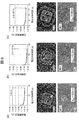
- 8A to 8C are graphs showing current values when a voltage is applied, the middle part is a TEM photograph showing the whole view of the SiNx membrane after dielectric breakdown, and the lower part is an enlargement of the formed nanopore. It is a photograph.
- the effective diameter d eff of the nanopore formed in Example 2 is 18.8 nm
- the effective diameter d eff of the nanopore formed in Example 3 is It was 13.2 nm
- the effective diameter d eff of the nanopore formed in Example 4 was 5.94 nm.
- the size of the nanopores formed can be adjusted by adjusting the current threshold value for stopping the voltage application. From the result of our research, it was found that the effective diameter d eff of the nanopore can be formed from about 1 nm to 200 nm or more by adjusting the current threshold value by the method of this embodiment. It was also found that even if the effective diameter d eff is increased, only a single nanopore is formed on the SiNx membrane.
- the KCl aqueous solution was used as the first aqueous solution 107 and the second aqueous solution 108.
- a single nanopore can be formed by using an aqueous solution of LiCl, NaCl, CaCl 2 , MgCl 2 , CsCl, or the like other than the KCl aqueous solution.
- the concentrations of the first aqueous solution 107 and the second aqueous solution 108 can be set to, for example, 1 M as in the above-described Experimental Examples 1 to 3, but may be higher than 1 M (eg, 1 M or more and 3 M or less), or 1 M or more.
- a single nanopore can be formed as long as it is thin (for example, 0.001 M or more and 1 M or less) and has a pH of 10 or more (more than pH 11 when the SiNx membrane has a film thickness of 20 nm or more).
- a SiNx membrane having a high withstand voltage (1 ⁇ x ⁇ 4/3) is used.
- the film density of the SiNx membrane is in the range of 2.8 g/cm 3 or more and 3.2 g/cm 3 or less.
- Those having a particularly high dielectric strength are suitable for nanopore measurement.
- the pH of the aqueous solution is 10 or more (SiNx membrane
- the current flowing between the electrodes is measured while continuously applying a constant voltage to the membrane, and the current value between the electrodes rapidly increases.
- a single nanopore can be formed by stopping the application of the voltage when a preset threshold current is reached (that is, the film has a dielectric breakdown).
- SiNx membranes with high dielectric strength (1 ⁇ x ⁇ 4/3) those with an etching rate of 0.5 nm/min or less due to hydrofluoric acid diluted to 1/200 have particularly high dielectric strength and are capable of measuring nanopores. Suitable for Of course, even if the etching rate by the hydrofluoric acid diluted to 1/200 is 0.5 nm/min or more, the pH of the aqueous solution is 10 or more (the film thickness of the SiNx membrane (1 ⁇ x ⁇ 4/3) is 20 nm). In the above case, if the pH is higher than 11, it is possible to form a single nanopore by the dielectric breakdown method.
- the thickness of the SiNx membrane 113 can be 5 nm or more and 100 nm or less.
- the dielectric breakdown voltage becomes lower as the film thickness of the SiNx membrane 113 becomes thinner, but especially when it becomes less than 5 nm, the rate of decrease of the dielectric breakdown voltage of the SiNx membrane 113 with respect to the film thickness decrease becomes large. As a result, the nanopore measurement may be hindered. Further, when the film thickness of the SiNx membrane 113 is larger than 100 nm, the voltage required for the dielectric breakdown exceeds 100 V, so that very large Joule heat is generated at the same time as the dielectric breakdown, and the SiNx membrane 113 is significantly deteriorated.
- Non-Patent Document 7 a method of applying 20 V to a SiNx membrane in a KCl aqueous solution having a pH of 7.5 and a concentration of 1 M, and stopping the voltage application when the current flowing between the electrodes reaches 10 ⁇ 6 A, A nanopore forming method in which a local thin film region is formed in a membrane, and then, as a second step, the local thin film region is penetrated by repeating pulse voltage application of 10 V and current measurement when 0.1 V is applied. Is disclosed. Compared to the present embodiment, the method of Non-Patent Document 7 requires a second step, and thus the time required to form the nanopore becomes longer.
- the nanopore forming method of the present embodiment takes less time to form the nanopores as compared with the method described in Non-Patent Document 7, and in the present embodiment, there are variations in the size of the nanopores formed. It was found that the size is small and the adjustable range of the size of the nanopore that can be formed is wide.
- a voltage is applied to the SiNx membrane (1 ⁇ x ⁇ 4/3) in an aqueous solution having a pH of 10 or more (the film thickness of the SiNx membrane is 20 nm or more).
- a single nanopore is applied to the SiNx membrane (1 ⁇ x ⁇ 4/3), which has a high withstand voltage and is suitable for nanopore measurement, by applying a voltage in an aqueous solution having a pH higher than 11) and causing dielectric breakdown. It can be stably formed.
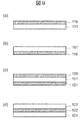
- FIG. 9 is a schematic diagram showing the structure of the laminated film according to the second embodiment.
- the film 118 is laminated on the upper surface of the SiNx film 101 (1 ⁇ x ⁇ 4/3).
- the film 119 is laminated on the lower surface of the SiNx film 101.
- the films 120 and 121 are laminated on both surfaces of the SiNx film 101.
- the film 122 is arranged between the two SiNx films 101.
- the films 118 to 122 are, for example, SiO 2 film, HfO 2 film, Al 2 O 3 film, HfAlO x film, ZrAlO x film, Ta 2 O 5 film, SiC film, SiCN film, carbon film, and composition ratio x is 1 It is composed of a SiNx film outside the range of ⁇ x ⁇ 4/3 or a composite thereof.
- the films 118 to 121 may be, for example, HMDS films for the purpose of preventing non-specific adsorption of the measurement target on the surface.
- the SiNx membrane (1 ⁇ x ⁇ 4/3) and the other membranes are laminated, if the pH is less than 10, a single membrane is formed on the membrane by the above-mentioned dielectric breakdown method. Cannot form nanopores.
- the pH of the aqueous solution is 10 or more (value greater than pH 11 when the film thickness of the SiNx membrane 113 is 20 nm or more)
- the SiNx film (1 ⁇ x ⁇ 4/3) is included in the laminated film. Can form a single nanopore.
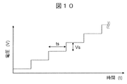
- FIG. 10 is a schematic diagram showing an example of voltage application in the third embodiment.
- the control unit 112 controls a power supply (not shown) so that the voltage applied between the electrodes 109 and 110 increases stepwise.
- t s indicates the application time of a certain voltage
- V s indicates the amount of voltage increase.
- the nanopore forming method of the present embodiment for example, by shortening t s or increasing V s , it is possible to shorten the time until the nanopores are formed. Further, the nanopore forming method according to the present embodiment is effective when it is unclear how much voltage the membrane to be used will cause dielectric breakdown. The size of the nanopore can be adjusted by adjusting the threshold current for cutting off the applied voltage.
- the control unit 112 further includes a voltmeter (not shown) for measuring the voltage between the electrodes 109 and 110.
- the voltage between the electrodes 109 and 110 is measured while controlling the voltage so that the current flowing between the electrodes 109 and 110 is constant, and after dielectric breakdown occurs, the electrodes are This is different from the first embodiment in that the current supply between the electrodes 109 and 110 is stopped when the voltage between 109 and 110 reaches a predetermined threshold voltage value.
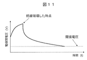
- FIG. 11 is a schematic diagram showing an example of voltage application in the fourth embodiment.
- the control unit 112 measures the voltage value while applying a voltage between the electrodes 109 and 110 so that the current flowing between the electrodes 109 and 110 is constant, and then, after the dielectric breakdown, the control unit 112 rapidly The control unit 112 stops the current supply between the electrodes 109 and 110 at the time when the inter-electrode voltage decreases and reaches a predetermined threshold voltage.
- a single nanopore can be formed in the SiNx membrane 113 also by such a method.
- the nanopore forming method according to the fifth embodiment will be described.
- only one of the first aqueous solution 107 and the second aqueous solution 108 has a pH of 10 or more (when the thickness of the SiNx membrane 113 is 20 nm or more, the pH is greater than 11), and the other has a pH of 10 or more. It is less than the first embodiment. Even in such a configuration, a single nanopore can be formed in the SiNx membrane 113 by the dielectric breakdown method.
- the pH of the aqueous solution on the side in contact with the negative electrode can be 10 or more.
- a 1 M KCl aqueous solution adjusted to pH 7.5 is introduced into the first chamber 105
- a 1 M KCl aqueous solution adjusted to pH 13 is introduced into the second chamber 106
- a potential difference is applied to the electrodes 109 and 110.
- a voltage can be applied to the SiNx membrane 113 by holding it.
- the electrode 109 has a higher potential than the electrode 110 (for example, the electrode 109 has 20 V and the electrode 110 has 0 V)
- the electrode 109 has a lower potential than the electrode 110 (for example, the electrode 109).
- the time until the nanopores are formed is shorter than that when 109 is set to -20V and the electrode 110 is set to 0V.
- one of the first aqueous solution 107 and the second aqueous solution 108 has a pH of 10 or higher, and the other aqueous solution has a pH of less than 10.
- the SiNx membrane having the composition ratio x of 1 ⁇ x ⁇ 4/3 has a pH of 7 or more when the pH of the first aqueous solution 107 and the pH of the second aqueous solution 108 are smaller than 10.
- the above-mentioned dielectric breakdown method has a property that nanopores are not formed.
- a single nanopore can be stably formed.
- either the first aqueous solution 107 or the second aqueous solution 108 is replaced with the aqueous solution containing the measurement object. After that, when the current value is measured while applying the voltage between the electrodes 109 and 110, the current value greatly changes when the measurement target passes through the nanopore.
- the structure begins to dissociate when the pH of the aqueous solution becomes 9.5 or higher.
- DNA begins to decompose in an acidic aqueous solution. Therefore, when the measurement target contains double-stranded DNA, the pH of the aqueous solution containing the measurement target is preferably 9 or less, and the pH may be in the range of 7 to 8 depending on the situation. ..
- the first aqueous solution 107 or the second aqueous solution 108 having a pH of 10 or more is added to a pH of 7 to 9 or a pH of 7 to 8
- the measurement object can be introduced into the aqueous solution.
- the measurement object is put in advance in the first aqueous solution 107 or the second aqueous solution 108 in the first chamber 105 or the second chamber 106.
- the nanopore can be measured as it is without replacing the aqueous solution in the first chamber 105 or the second chamber 106, and the time from the nanopore formation to the end of the nanopore measurement can be shortened. can do.
- the pH of the aqueous solution in one of the first chamber 105 and the second chamber 106 is adjusted to 7-9, and depending on the situation, the pH is adjusted to 7-8.
- the DNA will not dissociate even if an object to be measured containing the DNA having the double helix structure is previously placed therein. Therefore, after the nanopores are formed, the nanopores can be measured as they are without replacing the aqueous solution in the first chamber 105 or the second chamber 106, and the time from the formation of the nanopores to the end of the nanopore measurement can be shortened. it can.
- the present disclosure is not limited to the above-described embodiments and includes various modifications.
- the above-described embodiments have been described in detail in order to explain the present disclosure in an easy-to-understand manner, and it is not necessary to include all the configurations described.
- part of one embodiment can be replaced with the configuration of another embodiment.
- the configuration of another embodiment can be added to the configuration of one embodiment.
- a part of the configuration of each embodiment may be added, deleted, or replaced with a part of the configuration of another embodiment.
Landscapes
- Engineering & Computer Science (AREA)
- Chemical & Material Sciences (AREA)
- Health & Medical Sciences (AREA)
- Nanotechnology (AREA)
- Physics & Mathematics (AREA)
- Life Sciences & Earth Sciences (AREA)
- Analytical Chemistry (AREA)
- General Health & Medical Sciences (AREA)
- General Physics & Mathematics (AREA)
- Manufacturing & Machinery (AREA)
- Biomedical Technology (AREA)
- Crystallography & Structural Chemistry (AREA)
- Chemical Kinetics & Catalysis (AREA)
- Biochemistry (AREA)
- Immunology (AREA)
- Pathology (AREA)
- Microelectronics & Electronic Packaging (AREA)
- Condensed Matter Physics & Semiconductors (AREA)
- Organic Chemistry (AREA)
- Toxicology (AREA)
- Electrochemistry (AREA)
- Molecular Biology (AREA)
- Biophysics (AREA)
- Hematology (AREA)
- Spectroscopy & Molecular Physics (AREA)
- Urology & Nephrology (AREA)
- Food Science & Technology (AREA)
- Medicinal Chemistry (AREA)
- Computer Hardware Design (AREA)
- Investigating Or Analyzing Materials By The Use Of Electric Means (AREA)
- Apparatus Associated With Microorganisms And Enzymes (AREA)
- Measuring Or Testing Involving Enzymes Or Micro-Organisms (AREA)
- Physical Or Chemical Processes And Apparatus (AREA)
- Weting (AREA)
Abstract
L'invention concerne une technologie permettant la formation de manière stable des nanopores d'un type au moyen d'une rupture d'isolation dans une membrane qui a une tension de claquage d'isolation élevée. Un procédé de formation de nanopores selon la présente invention comprend : un procédé d'agencement d'une membrane SiNx entre une première solution aqueuse et une seconde solution aqueuse; un procédé pour amener une première électrode en contact avec la première solution aqueuse et amener une seconde électrode en contact avec la seconde solution aqueuse; et un procédé pour appliquer une tension à la première électrode et à la seconde électrode. Ce procédé de formation de nanopore est caractérisé en ce que : la membrane SiNx a un rapport de composition satisfaisant 1 < x < 4/3; et au moins l'une de la première solution aqueuse et de la seconde solution aqueuse a un pH de 10 ou plus.
Priority Applications (2)
| Application Number | Priority Date | Filing Date | Title |
|---|---|---|---|
| US17/297,132 US20220023822A1 (en) | 2018-12-12 | 2019-11-07 | Nanopore forming method and analysis method |
| CN201980076376.1A CN113164899A (zh) | 2018-12-12 | 2019-11-07 | 纳米孔形成方法及分析方法 |
Applications Claiming Priority (2)
| Application Number | Priority Date | Filing Date | Title |
|---|---|---|---|
| JP2018232501A JP7174614B2 (ja) | 2018-12-12 | 2018-12-12 | ナノポア形成方法及び分析方法 |
| JP2018-232501 | 2018-12-12 |
Publications (1)
| Publication Number | Publication Date |
|---|---|
| WO2020121697A1 true WO2020121697A1 (fr) | 2020-06-18 |
Family
ID=71076292
Family Applications (1)
| Application Number | Title | Priority Date | Filing Date |
|---|---|---|---|
| PCT/JP2019/043577 Ceased WO2020121697A1 (fr) | 2018-12-12 | 2019-11-07 | Procédé de formation de nanopores et procédé d'analyse |
Country Status (4)
| Country | Link |
|---|---|
| US (1) | US20220023822A1 (fr) |
| JP (1) | JP7174614B2 (fr) |
| CN (1) | CN113164899A (fr) |
| WO (1) | WO2020121697A1 (fr) |
Cited By (4)
| Publication number | Priority date | Publication date | Assignee | Title |
|---|---|---|---|---|
| CN112079330A (zh) * | 2020-09-07 | 2020-12-15 | 深圳市儒翰基因科技有限公司 | 固态纳米孔制造方法和包括固态纳米孔的传感器 |
| JP2022034857A (ja) * | 2020-08-19 | 2022-03-04 | 株式会社日立製作所 | 孔形成方法及び孔形成装置 |
| WO2023276129A1 (fr) * | 2021-07-01 | 2023-01-05 | 株式会社日立ハイテク | Procédé de formation de nanopores |
| EP4302870A4 (fr) * | 2021-03-03 | 2025-01-01 | Hitachi, Ltd. | Procédé de formation de pores et appareil de formation de pores |
Citations (8)
| Publication number | Priority date | Publication date | Assignee | Title |
|---|---|---|---|---|
| JPH04120733A (ja) * | 1990-09-12 | 1992-04-21 | Casio Comput Co Ltd | シリコン窒化膜の成膜方法 |
| JP2000193672A (ja) * | 1998-12-25 | 2000-07-14 | Olympus Optical Co Ltd | 走査型プロ―ブ顕微鏡用カンチレバ―およびその作製方法 |
| JP2011199062A (ja) * | 2010-03-19 | 2011-10-06 | Fujitsu Ltd | キャパシタ及び半導体装置 |
| US20150060276A1 (en) * | 2012-03-13 | 2015-03-05 | Peking University | Nanopore Control With Pressure and Voltage |
| WO2015097765A1 (fr) * | 2013-12-25 | 2015-07-02 | 株式会社日立製作所 | Procédé de formation de trou, appareil de mesure et jeu de puces |
| WO2016129111A1 (fr) * | 2015-02-13 | 2016-08-18 | 株式会社日立製作所 | Dispositif à membrane et procédé permettant de fabriquer ce dernier |
| US20180080072A1 (en) * | 2014-12-31 | 2018-03-22 | Coyote Bioscience Co., Ltd. | Detection of nucleic acid molecules using nanopores and tags |
| JP2018187626A (ja) * | 2012-05-07 | 2018-11-29 | ジ ユニバーシティ オブ オタワ | 高電界を用いたナノポアの作製 |
Family Cites Families (10)
| Publication number | Priority date | Publication date | Assignee | Title |
|---|---|---|---|---|
| JP2001028343A (ja) * | 1999-07-15 | 2001-01-30 | Hitachi Ltd | 薄膜処理方法及び液晶表示装置 |
| US7682924B2 (en) * | 2007-08-13 | 2010-03-23 | Micron Technology, Inc. | Methods of forming a plurality of capacitors |
| EP3268736B1 (fr) * | 2015-03-12 | 2021-08-18 | Ecole Polytechnique Fédérale de Lausanne (EPFL) | Procédé de formation de nanopore et utilisations de celui-ci |
| JP6261817B2 (ja) * | 2015-05-11 | 2018-01-17 | 株式会社日立製作所 | 分析デバイス及び分析方法 |
| CN113403604B (zh) * | 2015-07-31 | 2024-06-14 | 弗萨姆材料美国有限责任公司 | 用于沉积氮化硅膜的组合物和方法 |
| JP6730429B2 (ja) * | 2015-10-06 | 2020-07-29 | バーサム マテリアルズ ユーエス,リミティド ライアビリティ カンパニー | コンフォーマルな金属又はメタロイド窒化ケイ素膜の堆積方法 |
| JP6579948B2 (ja) * | 2015-12-24 | 2019-09-25 | 株式会社日立ハイテクノロジーズ | 生体ポリマを分析するための測定試薬及び分析デバイス |
| WO2017138149A1 (fr) * | 2016-02-12 | 2017-08-17 | 株式会社日立製作所 | Dispositif réservoir de solution |
| GB2565954B (en) * | 2016-06-10 | 2022-09-07 | Hitachi High Tech Corp | Method and apparatus for analyzing biomolecules |
| US11448638B2 (en) * | 2017-01-10 | 2022-09-20 | Hitachi High-Tech Corporation | Current measurement device and current measurement method using nanopore |
-
2018
- 2018-12-12 JP JP2018232501A patent/JP7174614B2/ja active Active
-
2019
- 2019-11-07 US US17/297,132 patent/US20220023822A1/en active Pending
- 2019-11-07 WO PCT/JP2019/043577 patent/WO2020121697A1/fr not_active Ceased
- 2019-11-07 CN CN201980076376.1A patent/CN113164899A/zh active Pending
Patent Citations (8)
| Publication number | Priority date | Publication date | Assignee | Title |
|---|---|---|---|---|
| JPH04120733A (ja) * | 1990-09-12 | 1992-04-21 | Casio Comput Co Ltd | シリコン窒化膜の成膜方法 |
| JP2000193672A (ja) * | 1998-12-25 | 2000-07-14 | Olympus Optical Co Ltd | 走査型プロ―ブ顕微鏡用カンチレバ―およびその作製方法 |
| JP2011199062A (ja) * | 2010-03-19 | 2011-10-06 | Fujitsu Ltd | キャパシタ及び半導体装置 |
| US20150060276A1 (en) * | 2012-03-13 | 2015-03-05 | Peking University | Nanopore Control With Pressure and Voltage |
| JP2018187626A (ja) * | 2012-05-07 | 2018-11-29 | ジ ユニバーシティ オブ オタワ | 高電界を用いたナノポアの作製 |
| WO2015097765A1 (fr) * | 2013-12-25 | 2015-07-02 | 株式会社日立製作所 | Procédé de formation de trou, appareil de mesure et jeu de puces |
| US20180080072A1 (en) * | 2014-12-31 | 2018-03-22 | Coyote Bioscience Co., Ltd. | Detection of nucleic acid molecules using nanopores and tags |
| WO2016129111A1 (fr) * | 2015-02-13 | 2016-08-18 | 株式会社日立製作所 | Dispositif à membrane et procédé permettant de fabriquer ce dernier |
Non-Patent Citations (2)
| Title |
|---|
| MATSUI, KAZUMA ET AL.: "Static charge outside chamber induces dielectric breakdown of solid- state nanopore membranes", JAPANESE JOURNAL OF APPLIED PHYSICS, vol. 57, no. 4, 19 March 2018 (2018-03-19), pages 046702.1 - 046702.8 * |
| YANAGI, ITARU ET AL.: "Two- step breakdown of a SiN membrane for nanopore fabrication: Formation of thin portion and penetration", THE 79TH JSAP AUTUMN MEETING , 2018 [PROCEEDINGS, 18 September 2018 (2018-09-18), pages 11 - 025 * |
Cited By (5)
| Publication number | Priority date | Publication date | Assignee | Title |
|---|---|---|---|---|
| JP2022034857A (ja) * | 2020-08-19 | 2022-03-04 | 株式会社日立製作所 | 孔形成方法及び孔形成装置 |
| JP7440375B2 (ja) | 2020-08-19 | 2024-02-28 | 株式会社日立製作所 | 孔形成方法及び孔形成装置 |
| CN112079330A (zh) * | 2020-09-07 | 2020-12-15 | 深圳市儒翰基因科技有限公司 | 固态纳米孔制造方法和包括固态纳米孔的传感器 |
| EP4302870A4 (fr) * | 2021-03-03 | 2025-01-01 | Hitachi, Ltd. | Procédé de formation de pores et appareil de formation de pores |
| WO2023276129A1 (fr) * | 2021-07-01 | 2023-01-05 | 株式会社日立ハイテク | Procédé de formation de nanopores |
Also Published As
| Publication number | Publication date |
|---|---|
| JP2020094894A (ja) | 2020-06-18 |
| US20220023822A1 (en) | 2022-01-27 |
| CN113164899A (zh) | 2021-07-23 |
| JP7174614B2 (ja) | 2022-11-17 |
Similar Documents
| Publication | Publication Date | Title |
|---|---|---|
| JP7174614B2 (ja) | ナノポア形成方法及び分析方法 | |
| JP6228613B2 (ja) | ナノポア形成方法、ナノポア形成装置及びセット | |
| Apel et al. | Diode-like single-ion track membrane prepared by electro-stopping | |
| Apel et al. | Effect of nanopore geometry on ion current rectification | |
| JP6472208B2 (ja) | 核酸搬送制御デバイス及びその製造方法、並びに核酸シーケンシング装置 | |
| US9128040B2 (en) | Nanopore device, method of fabricating the same, and DNA detection apparatus including the same | |
| JP2006523144A (ja) | 制御された導電性構造体のギャップの製造法 | |
| Coglitore et al. | Metal alloy solid-state nanopores for single nanoparticle detection | |
| EP3722794B1 (fr) | Procédé de formation de trou et dispositif associé | |
| Liu et al. | Order–disorder transition of anodic alumina nanochannel arrays grown under the guidance of focused-ion-beam patterning | |
| US10761057B2 (en) | Membrane device and method for manufacturing same | |
| WO2020105318A1 (fr) | Dispositif d'analyse de biomolécules et procédé d'analyse de biomolécules | |
| Olejniczak et al. | Variation in geometry and electrical conductance properties of asymmetric track-etched single nanopores: How uniform are they? | |
| Gaev et al. | Kinetics of crack formation in porous silicon | |
| Selvakumar et al. | A parametrical study of porous silicon for volatile organic chemical sensor applications | |
| Grose et al. | Transistor behavior via Au clusters etched from electrodes in an acidic gating solution: Metal nanoparticles mimicking conducting polymers | |
| US20190120792A1 (en) | Hydrophilic Substrate, Measuring Instrument, Device, and Hydrophilicity Retention Method | |
| Das | Nanostructure Engineering in Two-Dimensional Materials Beyond Graphene | |
| JP2006509645A (ja) | 固体特徴のパルスイオンビーム制御方法 | |
| US20240052507A1 (en) | Pore forming method and pore forming apparatus | |
| Xu et al. | Single-Molecule Detection Based on Graphene Cage-like Nanopores | |
| Masih Das | Nanostructure Engineering In Two-Dimensional Materials Beyond Graphene | |
| JP2024546760A (ja) | ナノ孔の製造方法 | |
| Bauer | Faculty of Physics and Astronomy | |
| Ma et al. | Shrinking Graphene Nanopore Using Electron-Beam-Induced Deposition for Single Molecule Detection |
Legal Events
| Date | Code | Title | Description |
|---|---|---|---|
| 121 | Ep: the epo has been informed by wipo that ep was designated in this application |
Ref document number: 19895617 Country of ref document: EP Kind code of ref document: A1 |
|
| NENP | Non-entry into the national phase |
Ref country code: DE |
|
| 122 | Ep: pct application non-entry in european phase |
Ref document number: 19895617 Country of ref document: EP Kind code of ref document: A1 |