WO2020174535A1 - Carte de circuit imprimé, dispositif à semi-conducteur, dispositif de conversion de puissance et corps mobile - Google Patents
Carte de circuit imprimé, dispositif à semi-conducteur, dispositif de conversion de puissance et corps mobile Download PDFInfo
- Publication number
- WO2020174535A1 WO2020174535A1 PCT/JP2019/007068 JP2019007068W WO2020174535A1 WO 2020174535 A1 WO2020174535 A1 WO 2020174535A1 JP 2019007068 W JP2019007068 W JP 2019007068W WO 2020174535 A1 WO2020174535 A1 WO 2020174535A1
- Authority
- WO
- WIPO (PCT)
- Prior art keywords
- circuit board
- electronic component
- resin
- semiconductor device
- temperature
- Prior art date
- Legal status (The legal status is an assumption and is not a legal conclusion. Google has not performed a legal analysis and makes no representation as to the accuracy of the status listed.)
- Ceased
Links
Images


Classifications
-
- H—ELECTRICITY
- H05—ELECTRIC TECHNIQUES NOT OTHERWISE PROVIDED FOR
- H05K—PRINTED CIRCUITS; CASINGS OR CONSTRUCTIONAL DETAILS OF ELECTRIC APPARATUS; MANUFACTURE OF ASSEMBLAGES OF ELECTRICAL COMPONENTS
- H05K1/00—Printed circuits
- H05K1/02—Details
- H05K1/0266—Marks, test patterns or identification means
- H05K1/0269—Marks, test patterns or identification means for visual or optical inspection
-
- H—ELECTRICITY
- H05—ELECTRIC TECHNIQUES NOT OTHERWISE PROVIDED FOR
- H05K—PRINTED CIRCUITS; CASINGS OR CONSTRUCTIONAL DETAILS OF ELECTRIC APPARATUS; MANUFACTURE OF ASSEMBLAGES OF ELECTRICAL COMPONENTS
- H05K1/00—Printed circuits
- H05K1/02—Details
- H05K1/0201—Thermal arrangements, e.g. for cooling, heating or preventing overheating
-
- H—ELECTRICITY
- H05—ELECTRIC TECHNIQUES NOT OTHERWISE PROVIDED FOR
- H05K—PRINTED CIRCUITS; CASINGS OR CONSTRUCTIONAL DETAILS OF ELECTRIC APPARATUS; MANUFACTURE OF ASSEMBLAGES OF ELECTRICAL COMPONENTS
- H05K3/00—Apparatus or processes for manufacturing printed circuits
- H05K3/22—Secondary treatment of printed circuits
- H05K3/28—Applying non-metallic protective coatings
- H05K3/284—Applying non-metallic protective coatings for encapsulating mounted components
Definitions
- the present invention relates to a circuit board.
- the present invention also relates to a semiconductor device, a power conversion device, and a moving body that include a circuit board.
- Circuit boards often include printed circuit boards and multiple electronic components.
- the plurality of electronic components are mounted on the printed board.
- the composition is arranged near the surface in order to indicate whether the surface has exceeded the threshold temperature (page 194, lower right column, line 12-14). Line).
- the composition becomes transparent, and when the surface falls below the threshold temperature, the composition becomes opaque (page 194, lower right column, lines 14 to 16).
- the composition comprises a transparent flexible matrix material and an indicator material dispersed in the matrix material (page 195, upper right column, lines 1- 3).
- the instruction material is granular (page 196, upper left column, line 7 to line 8).
- the instruction material may be wax (page 196, upper right column, line 5 to line 6).
- the above-mentioned problem becomes prominent when the circuit board is a control board that controls power semiconductor elements.
- the circuit board is the control board for controlling the power semiconductor element
- the control board for controlling the power semiconductor element is often a product of high-mix low-volume production.
- the position where electronic components are mounted often differs depending on the type of circuit board, and the time required to determine whether or not there is a defect in the circuit board tends to be long. Is.
- the circuit board may be required to visually check whether the circuit board has been exposed to heat. For example, it may be required to visually confirm whether or not the circuit board has been exposed to heat in order to identify whether or not the heat stress test has been performed on the circuit board. In that case, it is possible to visually confirm whether or not the circuit board is exposed to heat by contacting the circuit board with a material that causes a visual change when the temperature rises.
- it is not possible to properly confirm whether or not the heat generated by one of the electronic components included in the plurality of electronic components is transmitted to the material and the circuit board is exposed to the heat. For example, there is a case where it is not possible to properly confirm whether or not the circuit board is exposed to heat by transmitting heat generated by the electronic component that generates heat during normal operation to the material.
- the present invention has been made in view of these problems.
- the problem to be solved by the present invention is to provide a circuit board that can easily visually confirm whether or not the first electronic component has generated heat independently of whether or not the second electronic component has generated heat. It is to be.
- another problem to be solved by the present invention is to provide a circuit board capable of easily visually confirming whether or not the circuit board is exposed to heat independently of whether or not the electronic component generates heat. It is to be.
- the present invention is directed to a circuit board.
- the circuit board includes a printed circuit board, a first electronic component, a second electronic component, and a temperature indicating resin.
- the first electronic component and the second electronic component are mounted on a printed board.
- the thermosensitive resin contacts the first electronic component but does not contact the second electronic component.
- the thermosensitive resin undergoes a visual change when the temperature rises.
- the circuit board includes a printed board, an electronic component, and a temperature indicating resin.
- Electronic components are mounted on a printed circuit board.
- the thermosensitive resin contacts the printed circuit board but does not contact the electronic components.
- the thermosensitive resin undergoes a visual change when the temperature rises.
- the present invention is also applied to a semiconductor device, a power conversion device, and a moving body.
- the second electronic component when the second electronic component generates heat, no visual change occurs in the temperature indicating resin, but when the first electronic component generates heat, the temperature indicating resin does not change. A visual change occurs. Therefore, it is possible to visually confirm whether or not the first electronic component has generated heat independently of whether or not the second electronic component has generated heat.
- the temperature indicating resin when the electronic component generates heat, the temperature indicating resin does not change visually, but when the circuit board is exposed to heat, the temperature indicating resin changes visually. Occurs. Therefore, it is possible to visually confirm whether or not the circuit board is exposed to heat independently of whether or not the electronic component generates heat.
- FIG. 3 is a cross-sectional view schematically illustrating the circuit board according to the first embodiment.
- FIG. 3 is an enlarged cross-sectional view schematically showing a part of the circuit board according to the first embodiment.
- FIG. 3 is an enlarged cross-sectional view schematically showing a part of the circuit board according to the first embodiment.
- FIG. 3 is an enlarged cross-sectional view schematically showing a part of the circuit board according to the first embodiment.
- FIG. 7 is a plan view schematically showing the circuit board according to the second embodiment.
- FIG. 9 is a diagram schematically showing a semiconductor device according to a third embodiment. It is a block diagram which shows the structure of the power conversion system of Embodiment 4. It is a side view which illustrates the moving body of Embodiment 5 typically. It is sectional drawing which illustrates the circuit board of a reference example typically.
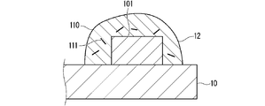
- FIG. 1 is a sectional view schematically showing the circuit board according to the first embodiment.
- the circuit board 1 according to the first embodiment illustrated in FIG. 1 includes a printed board 10 and a plurality of electronic components 11.
- a plurality of electronic components 11 are mounted on the printed circuit board 10.
- the plurality of electronic components 11 to be mounted are electrically connected to the wiring pattern provided on the printed board 10.
- an electronic circuit including the plurality of electronic components 11 and the wiring pattern provided on the printed circuit board 10 is configured.
- Each of the plurality of electronic components 11 is an active component or a passive component.
- Each of the plurality of electronic components 11 is a transistor, a diode, an integrated circuit (IC), a capacitor, a coil, a resistor, an inductor, a transformer, or the like.
- the plurality of electronic components 11 include a first electronic component 101 and a second electronic component 102.
- the first electronic component 101 and the second electronic component 102 have different heat generation characteristics.
- the circuit board 1 includes a temperature indicating resin 12.
- the temperature-sensitive resin 12 undergoes a visual change when the temperature rises.
- the temperature indicating resin 12 is applied on the first electronic component 101, but not applied on the second electronic component 102. Therefore, the thermosensitive resin 12 contacts the first electronic component 101, but does not contact the second electronic component 102.
- the temperature indicating resin 12 does not change visually. Occurs. Therefore, it is possible to visually confirm whether or not the first electronic component 101 has generated heat independently of whether or not the second electronic component 102 has generated heat.
- the first electronic component 101 is preferably an electronic component that does not generate heat during normal operation.
- the second electronic component 102 is preferably an electronic component that generates heat during normal operation.
- the first electronic component 101 that does not generate heat during normal operation is a normal product
- the first electronic component 101 does not generate heat and a visual change occurs in the temperature indicating resin 12 that contacts the first electronic component 101. Absent.
- the first electronic component 101 may generate heat, and the temperature indicating resin 12 that contacts the first electronic component 101 is visually detected. Changes may occur.
- the state of the temperature indicating resin 12 is not affected by the heat generation of the second electronic component 102 that generates heat during normal operation. Accordingly, it is possible to visually confirm whether or not the first electronic component 101 that does not generate heat during normal operation is an abnormal product. Further, whether or not the first electronic component 101 that does not generate heat during normal operation is an abnormal product is not affected by the heat generated by the second electronic component 102 that generates heat during normal operation.
- the quality of the circuit board 1 can be improved and the loss cost of the circuit board 1 can be reduced. Further, the time required to investigate the cause of the defect of the circuit board 1 can be shortened, and the work of investigating the cause of the defect of the circuit board 1 can be simplified. These contribute to improving the productivity of the circuit board 1.
- the above-mentioned effects are remarkable when the circuit board 1 is a control board for controlling the power semiconductor element.
- the circuit board 1 is a control board for controlling a power semiconductor element, the above-described effects are remarkable.
- the control board for controlling the power semiconductor element is often a product of a large variety of products, and therefore, the circuit board.
- 1 is a control board for controlling the power semiconductor element, the position where the electronic component is mounted is often different depending on the product type, and the time required to determine whether the circuit board 1 is defective tends to be long. Is.
- the first electronic component 101 is preferably a passive component.
- the temperature indicating resin 12 only needs to be applied to the passive component, so that the time required to apply the temperature indicating resin 12 can be shortened. The usage amount of 12 can be reduced. This contributes to reducing the cost of the circuit board 1.
- 2, 3 and 4 are enlarged cross-sectional views schematically showing a part of the circuit board according to the first embodiment. 2, 3 and 4 illustrate a first example, a second example and a third example of the temperature indicating resin, respectively.
- the temperature indicating resin 12 includes a resin 110 and a temperature indicating material 111, as shown in FIGS. 2, 3, and 4.
- the temperature indicating material is also called an indicating material or the like.
- the temperature indicator 111 is embedded in the resin 110.
- the temperature indicating material 111 reacts at a temperature equal to or higher than a specific temperature higher than room temperature. For example, the temperature indicating material 111 melts at a temperature equal to or higher than the specific temperature.
- the first electronic component 101 generates heat
- the heat generation of the first electronic component 101 is transmitted to the temperature indicating material 111
- the temperature of the temperature indicating material 111 reaches a temperature equal to or higher than the specific temperature
- the temperature indicating material 111 melts. Accordingly, when the temperature of the temperature indicating material 111 returns to a temperature lower than the specific temperature and the temperature indicating material 111 solidifies, a visual change occurs in the temperature indicating resin 12.
- the resin 110 is a polyolefin resin or the like.
- the temperature indicator 111 is wax or the like.
- the temperature indicating material 111 is granular wax.
- the temperature indicator 111 is woven into the resin before curing to prepare a mixture of the resin before curing and the temperature indicator 111, and the prepared mixture is applied and applied. The mixture is cured.
- the temperature indicator 111 is a plate-shaped wax.
- the work of weaving the temperature indicating material 111 into the resin before curing is unnecessary, the work of applying the temperature indicating resin 12 can be simplified. This contributes to improving the productivity of the circuit board 1.
- the temperature indicator 111 is flaky wax.
- the sensitivity of the temperature indicating resin 12 to changes in temperature is improved.
- FIG. 9 is a cross-sectional view schematically illustrating the circuit board of the reference example.
- FIG. 9A illustrates a state in which neither the first electronic component nor the second electronic component is generating heat.
- FIG. 9B illustrates a state in which the first electronic component is not generating heat but the second electronic component is generating heat.
- the temperature-indicating resin 12 is applied on the first electronic component 101, but not on the second electronic component 102. .. Therefore, the thermosensitive resin 12 contacts the first electronic component 101 but does not contact the second electronic component 102.
- the second electronic component 102 generates heat
- there is no visual change in the temperature indicating resin 12 but when the first electronic component 101 generates heat, there is a visual change in the temperature indicating resin. Occurs. Therefore, it is possible to visually confirm whether or not the first electronic component 101 has generated heat independently of whether or not the second electronic component 102 has generated heat.
- the temperature indicating resin 12 is applied on the first electronic component 101 and the second electronic component 102. Therefore, the thermosensitive resin 12 comes into contact with the first electronic component 101 and the second electronic component 102. As a result, when the second electronic component 102 generates heat, whether the first electronic component 101 generates heat or not, as shown in FIG. Changes occur. Therefore, whether or not the first electronic component 101 has generated heat cannot be appropriately visually confirmed independently of whether or not the second electronic component 102 has generated heat.
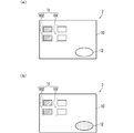
- FIG. 5 is a plan view schematically showing the circuit board according to the second embodiment.
- FIG. 5A illustrates a state before the thermal stress test is performed on the circuit board.
- FIG. 5B illustrates a state after the thermal stress test is performed on the circuit board.
- the circuit board 2 of the second embodiment shown in FIG. 5 is different from the circuit board 1 of the first embodiment shown in FIG. 1 mainly in the following differences. Regarding the points not described, the same configuration as that adopted in the circuit board 1 of the first embodiment is also adopted in the circuit board 2 of the second embodiment.
- the temperature-sensitive resin 12 is applied on the first electronic component 101 included in the plurality of electronic components 11, but the second temperature component included in the plurality of electronic components 11 is applied. It is not coated on the electronic component 102. Therefore, the thermosensitive resin 12 contacts the first electronic component 101, but does not contact the second electronic component 102.
- the temperature indicating resin 12 is applied on the printed circuit board 10 but not on the plurality of electronic components 11. Therefore, the temperature indicating resin 12 contacts the printed circuit board 10, but does not contact the plurality of electronic components 11.
- thermosensitive resin 12 contacts the printed circuit board 10, but does not contact the plurality of electronic components 11. For this reason, the temperature indicating resin 12 contacts the portion where the temperature rises when the thermal stress test is performed on the circuit board 1, but the temperature may rise other than when the thermal stress test is performed. Do not come into contact with any parts that have potential Therefore, when the heat stress test is performed on the circuit board 1, the heat applied to the circuit board 1 by the heat stress test is transmitted to the temperature indicating material 111, and the temperature of the temperature indicating material 111 becomes higher than room temperature. The temperature indicating material 111 melts. As a result, when the temperature of the temperature indicating material 111 returns to room temperature and the temperature indicating material 111 solidifies, a visual change occurs in the temperature indicating resin 12. Therefore, by visually confirming whether or not the circuit board 1 is exposed to heat, it is possible to identify whether or not the thermal stress test is performed on the circuit board 1. This contributes to preventing omission of the step of performing the thermal stress test when manufacturing the circuit board 1.
- FIG. 6 is a diagram schematically showing the semiconductor device of the third embodiment.
- the semiconductor device 3 according to the third embodiment shown in FIG. 6 is a power semiconductor, and as shown in FIG. 6A, is a semiconductor module including a semiconductor element 30, a semiconductor discrete component, or the like.
- the semiconductor element 30 is a switching element, a diode, or the like.
- the semiconductor device 3 includes the circuit board 2 of the second embodiment.
- the semiconductor device 3 may include the circuit board 1 of the first embodiment instead of the circuit board 2 of the second embodiment.
- the circuit board 2 is built in the semiconductor device 3.
- the semiconductor device 3 has an exterior 31.
- the outer package 31 desirably has an opening 300 that faces the temperature indicating resin 12.
- the opening 300 is an opening for confirming the state of the temperature indicating resin 12. Therefore, the temperature indicating resin 12 can be visually recognized from the outside of the exterior 31 via the opening 300. Thereby, after the semiconductor device 3 is assembled and the circuit board 2 is built in the semiconductor device 3, the state of the temperature indicating resin 12 can be confirmed, and it can be visually confirmed whether or not the circuit board 1 is exposed to heat. By doing so, it is possible to identify whether or not the thermal stress test is performed on the circuit board 1. Therefore, the state of the temperature-sensitive resin 12 can be used as evidence presented to the shipping destination of the semiconductor device 3 that the circuit board 1 has been subjected to the thermal stress test.
- the semiconductor element 30 is preferably a semiconductor element including a wide band gap semiconductor.
- the wide band gap semiconductor is silicon carbide (SiC), gallium nitride (GaN), diamond (C), or the like.
- Wide bandgap semiconductors such as silicon carbide (SiC), gallium nitride (GaN), and diamond (C) have a wider bandgap than that of semiconductors such as silicon (Si).
- the semiconductor element including the wide band gap semiconductor can stably ensure the electrode ultrasonic bonding life even when used in a high temperature environment. Further, the space occupied by the semiconductor element 30 can be reduced, and the semiconductor device 3 can be reduced in size and weight.
- the circuit board 1 of the first embodiment, the circuit board 2 of the second embodiment, or the semiconductor device 3 of the third embodiment described above is applied to a power conversion device.
- the application of the circuit board 1 of the first embodiment, the circuit board 2 of the second embodiment, or the semiconductor device 3 of the third embodiment is not limited to a specific power conversion device, but the fourth embodiment will be described below.
- the case where the circuit board 1 of the first embodiment, the circuit board 2 of the second embodiment, or the semiconductor device 3 of the third embodiment is applied to a three-phase inverter will be described.
- FIG. 7 is a block diagram showing the configuration of the power conversion system according to the fourth embodiment.
- the power conversion system shown in FIG. 7 includes a power supply 40, a power conversion device 41, and a load 42.
- the power supply 40 is a DC power supply and supplies DC power to the power converter 41.
- the power supply 40 can be configured by various things, for example, a DC system, a solar battery, a storage battery, or a rectifier circuit or an AC/DC converter connected to an AC system. Good. Further, the power supply 40 may be configured by a DC/DC converter that converts DC power output from the DC system into predetermined power.
- the power conversion device 41 is a three-phase inverter connected between the power supply 40 and the load 42, converts the DC power supplied from the power supply 40 into AC power, and supplies the AC power to the load 42.
- the power conversion device 41 includes a main conversion circuit 400 that converts DC power into AC power and outputs the converted power, and a drive circuit 401 that outputs a drive signal that drives each switching element of the main conversion circuit 400.
- a control circuit 402 that outputs a control signal for controlling the drive circuit 401 to the drive circuit 401.
- At least one of the main conversion circuit 400, the drive circuit 401, and the control circuit 402 may include the circuit board 1 of the first embodiment or the circuit board 2 of the second embodiment described above.
- the load 42 is a three-phase electric motor driven by the AC power supplied from the power converter 41.
- the load 42 is not limited to a specific use, and is an electric motor mounted in various electric devices, and is used as, for example, a hybrid car, an electric car, a railway vehicle, an elevator, or an electric motor for an air conditioner.
- the main conversion circuit 400 includes a switching element and a free wheeling diode (not shown), and the switching element switches to convert the DC power supplied from the power supply 40 into AC power and supply the AC power to the load 42.
- the main conversion circuit 400 is a two-level three-phase full bridge circuit, and includes six switching elements and respective switching elements. It can consist of six freewheeling diodes in anti-parallel.
- Each switching element of the main conversion circuit 400 may include the circuit board 1 of the first embodiment or the circuit board 2 of the second embodiment.
- the semiconductor device 3 of the third embodiment described above may be applied to each switching element of the main conversion circuit 400.
- the six switching elements are connected in series for every two switching elements to configure upper and lower arms, and each upper and lower arm configures each phase (U phase, V phase, W phase) of the full bridge circuit.
- the output terminals of the upper and lower arms that is, the three output terminals of the main conversion circuit 400 are connected to the load 42.
- the drive circuit 401 generates a drive signal for driving the switching element of the main conversion circuit 400 and supplies it to the control electrode of the switching element of the main conversion circuit 400. Specifically, a drive signal for turning on the switching element and a drive signal for turning off the switching element are output to the control electrodes of the respective switching elements according to a control signal from the control circuit 402 described later.
- the drive signal is a voltage signal (ON signal) that is equal to or higher than the threshold voltage of the switching element
- the drive signal is a voltage that is equal to or lower than the threshold voltage of the switching element. It becomes a signal (off signal).
- the control circuit 402 controls the switching elements of the main conversion circuit 400 so that desired power is supplied to the load 42. Specifically, the time (ON time) in which each switching element of the main conversion circuit 400 should be in the ON state is calculated based on the power to be supplied to the load 42.
- the main conversion circuit 400 can be controlled by PWM control that modulates the ON time of the switching element according to the voltage to be output.
- a control command (control signal) is output to the drive circuit 401 so that an ON signal is output to the switching element that should be in the ON state and an OFF signal is output to the switching element that should be in the OFF state.
- the drive circuit 401 outputs an ON signal or an OFF signal as a drive signal to the control electrode of each switching element according to this control signal.
- At least one of the main conversion circuit 400, the drive circuit 401, and the control circuit 402 includes the circuit board 1 of the first embodiment or the circuit board 2 of the second embodiment described above. , Visually confirming whether or not the first electronic component 101 has generated heat independently of whether or not the second electronic component 102 has generated heat, or whether or not any of the plurality of electronic components 11 has generated heat. Independently from this, it is possible to visually confirm whether or not the circuit board 2 is exposed to heat.
- circuit board 1 of the first embodiment, the circuit board 2 of the second embodiment, or the semiconductor device 3 of the third embodiment is applied to a two-level three-phase inverter.
- the application of the circuit board 1 of the first embodiment, the circuit board 2 of the second embodiment, or the semiconductor device 3 of the third embodiment is not limited to this, and can be applied to various power conversion devices.
- a two-level power conversion device is used, but a three-level or multi-level power conversion device may be used. If power is supplied to a single-phase load, a single-phase inverter is used.
- the circuit board 1 according to the first embodiment, the circuit board 2 according to the second embodiment, or the semiconductor device 3 according to the third embodiment may be applied.
- the circuit board 1 according to the first embodiment, the circuit board 2 according to the second embodiment, or the semiconductor device 3 according to the third embodiment is used for the DC/DC converter or the AC/DC converter. It is also possible to apply
- the power conversion device to which the circuit board 1 of the first embodiment, the circuit board 2 of the second embodiment, or the semiconductor device 3 of the third embodiment is applied is not limited to the case where the above-mentioned load is an electric motor. Instead, for example, it can be used as a power supply device for an electric discharge machine, a laser machine, an induction heating cooker, or a non-contact power supply system, and can also be used as a power conditioner for a solar power generation system, a power storage system, or the like. Is.
- the cooler and the like of the main conversion circuit 400 can be downsized and lightened, and the power converter 41 can be achieved. Can be improved, and energy consumed by the main conversion circuit 400 can be reduced.
- FIG. 8 is a side view schematically showing the moving body according to the fifth embodiment.
- the moving body 5 illustrated in FIG. 8 is a train.
- the moving body 5 may be other than the train.
- the moving body 5 may be an automobile, a ship, an aircraft, a power-assisted bicycle, an electric wheelchair, or the like.
- the mobile unit 5 includes the power conversion device 41 of the fourth embodiment.
- the moving body 5 drives a motor or the like by the electric power converted by the power converter 41.
- the moving body 5 When the downsized and lightened semiconductor device is applied to the power converter 41 of the fourth embodiment, the moving body 5 can be downsized and lightened, and the efficiency of the moving body 5 can be improved. Therefore, the performance of the moving body 5 can be improved.
Landscapes
- Engineering & Computer Science (AREA)
- Microelectronics & Electronic Packaging (AREA)
- Structure Of Printed Boards (AREA)
- Inverter Devices (AREA)
- Non-Metallic Protective Coatings For Printed Circuits (AREA)
Abstract
La présente invention facilite la confirmation visuelle du fait qu'un premier composant électronique a généré de la chaleur indépendamment du fait qu'un second composant électronique a généré de la chaleur, ou du fait qu'une carte de circuit imprimé a été exposée à la chaleur. Le premier composant électronique et le second composant électronique sont montés sur une carte de circuit imprimé. Une résine thermochromique entre en contact avec le premier composant électronique mais ne vient pas en contact avec le second composant électronique. Un changement visuel se produit dans la résine thermochromique lorsque la température augmente. En variante, un composant électronique est monté sur la carte de circuit imprimé. La résine thermochromique entre en contact avec la carte de circuit imprimé mais ne vient pas en contact avec le composant électronique. Un changement visuel se produit dans la résine thermochromique lorsque la température augmente.
Priority Applications (5)
| Application Number | Priority Date | Filing Date | Title |
|---|---|---|---|
| CN201980092667.XA CN113455112A (zh) | 2019-02-25 | 2019-02-25 | 电路基板、半导体装置、电力转换装置及移动体 |
| JP2021501393A JPWO2020174535A1 (ja) | 2019-02-25 | 2019-02-25 | 回路基板、半導体装置、電力変換装置及び移動体 |
| PCT/JP2019/007068 WO2020174535A1 (fr) | 2019-02-25 | 2019-02-25 | Carte de circuit imprimé, dispositif à semi-conducteur, dispositif de conversion de puissance et corps mobile |
| US17/290,461 US12075556B2 (en) | 2019-02-25 | 2019-02-25 | Circuit board, semiconductor device, power converter, and moving object |
| DE112019006914.4T DE112019006914T5 (de) | 2019-02-25 | 2019-02-25 | Platine, Halbleitervorrichtung, Leistungswandler und sich bewegendes Objekt |
Applications Claiming Priority (1)
| Application Number | Priority Date | Filing Date | Title |
|---|---|---|---|
| PCT/JP2019/007068 WO2020174535A1 (fr) | 2019-02-25 | 2019-02-25 | Carte de circuit imprimé, dispositif à semi-conducteur, dispositif de conversion de puissance et corps mobile |
Publications (1)
| Publication Number | Publication Date |
|---|---|
| WO2020174535A1 true WO2020174535A1 (fr) | 2020-09-03 |
Family
ID=72239066
Family Applications (1)
| Application Number | Title | Priority Date | Filing Date |
|---|---|---|---|
| PCT/JP2019/007068 Ceased WO2020174535A1 (fr) | 2019-02-25 | 2019-02-25 | Carte de circuit imprimé, dispositif à semi-conducteur, dispositif de conversion de puissance et corps mobile |
Country Status (5)
| Country | Link |
|---|---|
| US (1) | US12075556B2 (fr) |
| JP (1) | JPWO2020174535A1 (fr) |
| CN (1) | CN113455112A (fr) |
| DE (1) | DE112019006914T5 (fr) |
| WO (1) | WO2020174535A1 (fr) |
Citations (5)
| Publication number | Priority date | Publication date | Assignee | Title |
|---|---|---|---|---|
| JPS5931268U (ja) * | 1982-08-20 | 1984-02-27 | 日本電気ホームエレクトロニクス株式会社 | プリント基板装置 |
| JPH01112123A (ja) * | 1986-04-07 | 1989-04-28 | Raychem Corp | 可逆的温度指示組成物 |
| JPH01157501A (ja) * | 1987-09-29 | 1989-06-20 | Toshiba Corp | 電子部品 |
| JP2006005669A (ja) * | 2004-06-17 | 2006-01-05 | Nec Saitama Ltd | 携帯電話の不具合原因検出方法 |
| US20150173178A1 (en) * | 2013-12-12 | 2015-06-18 | Echostar Technologies L.L.C. | Thermochromic solder mask for electronic devices |
Family Cites Families (13)
| Publication number | Priority date | Publication date | Assignee | Title |
|---|---|---|---|---|
| JPS59126643A (ja) | 1983-01-07 | 1984-07-21 | Matsushita Electric Ind Co Ltd | 電子回路の被覆方法 |
| US4891250A (en) * | 1988-02-17 | 1990-01-02 | Weibe Edward W | Electronic component operating temperature indicator |
| JPH05299793A (ja) * | 1992-04-17 | 1993-11-12 | Sony Corp | プリント配線板 |
| JPH09283307A (ja) | 1996-04-12 | 1997-10-31 | Matsushita Electric Ind Co Ltd | サージ吸収器 |
| JPH1112123A (ja) | 1997-06-25 | 1999-01-19 | Nitto Denko Corp | 水賦活脱毛シート |
| JP2000223830A (ja) | 1999-01-28 | 2000-08-11 | Sony Corp | プリント配線板 |
| JP2001023850A (ja) | 1999-07-06 | 2001-01-26 | Guangqi Science & Technol Co Ltd | カラー変化により良否を判別される電子素子 |
| JP2002117689A (ja) | 2000-10-10 | 2002-04-19 | Ricoh Microelectronics Co Ltd | 処理対象物の処理有無確認方法及びプリント基板 |
| JP4475988B2 (ja) | 2004-03-11 | 2010-06-09 | Hoya株式会社 | プリント基板 |
| JP2007073604A (ja) | 2005-09-05 | 2007-03-22 | Densei Lambda Kk | プリント基板及びプリント基板の製造方法並びにプリント基板の識別方法 |
| JP2008060430A (ja) * | 2006-08-31 | 2008-03-13 | Daikin Ind Ltd | 電力変換装置 |
| JP2008166310A (ja) * | 2006-12-26 | 2008-07-17 | Toshiba Corp | 半田印刷マスク、プリント配線基板及び回路基板の製造方法 |
| JP6912560B2 (ja) | 2017-04-19 | 2021-08-04 | 三菱電機株式会社 | 半導体モジュールおよび電力変換装置 |
-
2019
- 2019-02-25 DE DE112019006914.4T patent/DE112019006914T5/de active Pending
- 2019-02-25 JP JP2021501393A patent/JPWO2020174535A1/ja active Pending
- 2019-02-25 US US17/290,461 patent/US12075556B2/en active Active
- 2019-02-25 CN CN201980092667.XA patent/CN113455112A/zh active Pending
- 2019-02-25 WO PCT/JP2019/007068 patent/WO2020174535A1/fr not_active Ceased
Patent Citations (5)
| Publication number | Priority date | Publication date | Assignee | Title |
|---|---|---|---|---|
| JPS5931268U (ja) * | 1982-08-20 | 1984-02-27 | 日本電気ホームエレクトロニクス株式会社 | プリント基板装置 |
| JPH01112123A (ja) * | 1986-04-07 | 1989-04-28 | Raychem Corp | 可逆的温度指示組成物 |
| JPH01157501A (ja) * | 1987-09-29 | 1989-06-20 | Toshiba Corp | 電子部品 |
| JP2006005669A (ja) * | 2004-06-17 | 2006-01-05 | Nec Saitama Ltd | 携帯電話の不具合原因検出方法 |
| US20150173178A1 (en) * | 2013-12-12 | 2015-06-18 | Echostar Technologies L.L.C. | Thermochromic solder mask for electronic devices |
Also Published As
| Publication number | Publication date |
|---|---|
| CN113455112A (zh) | 2021-09-28 |
| US20210378085A1 (en) | 2021-12-02 |
| DE112019006914T5 (de) | 2021-11-04 |
| JPWO2020174535A1 (ja) | 2021-09-13 |
| US12075556B2 (en) | 2024-08-27 |
Similar Documents
| Publication | Publication Date | Title |
|---|---|---|
| JP6783327B2 (ja) | 半導体装置および電力変換装置 | |
| JP7196815B2 (ja) | 半導体モジュール及び電力変換装置 | |
| US10121732B2 (en) | Semiconductor device and electric power conversion device having relay terminal directly fixed to an insulating film of base plate | |
| JP7091878B2 (ja) | パワーモジュール、電力変換装置、及びパワーモジュールの製造方法 | |
| JP2019140233A (ja) | パワーモジュールおよび電力変換装置 | |
| JP2019083283A (ja) | 半導体モジュール、その製造方法及び電力変換装置 | |
| JP2020107666A (ja) | 半導体モジュール、その製造方法及び電力変換装置 | |
| CN108538793A (zh) | 半导体功率模块及电力变换装置 | |
| JP6896831B2 (ja) | 半導体モジュールおよび電力変換装置 | |
| JP6827404B2 (ja) | 半導体装置および電力変換装置 | |
| CN116171490A (zh) | 半导体装置、电力变换装置、移动体以及半导体装置的制造方法 | |
| WO2020174535A1 (fr) | Carte de circuit imprimé, dispositif à semi-conducteur, dispositif de conversion de puissance et corps mobile | |
| US20240087968A1 (en) | Semiconductor device, method of manufacturing semiconductor device, and power conversion apparatus | |
| US11990447B2 (en) | Semiconductor device and power conversion device | |
| US20230335455A1 (en) | Semiconductor device, power conversion device, and mobile body | |
| JP7396264B2 (ja) | 半導体モジュール及び電力変換装置 | |
| JP7150183B2 (ja) | 半導体装置、電力変換装置及び移動体 | |
| US20240038638A1 (en) | Power electronics module | |
| JP7268760B2 (ja) | 半導体モジュール、電力変換装置及び移動体 | |
| US11887904B2 (en) | Integrally bonded semiconductor device and power converter including the same | |
| WO2023175854A1 (fr) | Dispositif à semi-conducteur, convertisseur de puissance et procédé de fabrication de dispositif à semi-conducteur |
Legal Events
| Date | Code | Title | Description |
|---|---|---|---|
| 121 | Ep: the epo has been informed by wipo that ep was designated in this application |
Ref document number: 19916659 Country of ref document: EP Kind code of ref document: A1 |
|
| ENP | Entry into the national phase |
Ref document number: 2021501393 Country of ref document: JP Kind code of ref document: A |
|
| 122 | Ep: pct application non-entry in european phase |
Ref document number: 19916659 Country of ref document: EP Kind code of ref document: A1 |