WO2020194812A1 - Varistance stratifiée - Google Patents
Varistance stratifiée Download PDFInfo
- Publication number
- WO2020194812A1 WO2020194812A1 PCT/JP2019/040562 JP2019040562W WO2020194812A1 WO 2020194812 A1 WO2020194812 A1 WO 2020194812A1 JP 2019040562 W JP2019040562 W JP 2019040562W WO 2020194812 A1 WO2020194812 A1 WO 2020194812A1
- Authority
- WO
- WIPO (PCT)
- Prior art keywords
- pair
- layer
- high resistance
- varistor
- sintered body
- Prior art date
- Legal status (The legal status is an assumption and is not a legal conclusion. Google has not performed a legal analysis and makes no representation as to the accuracy of the status listed.)
- Ceased
Links
Images


Classifications
-
- H—ELECTRICITY
- H01—ELECTRIC ELEMENTS
- H01C—RESISTORS
- H01C7/00—Non-adjustable resistors formed as one or more layers or coatings; Non-adjustable resistors made from powdered conducting material or powdered semi-conducting material with or without insulating material
- H01C7/10—Non-adjustable resistors formed as one or more layers or coatings; Non-adjustable resistors made from powdered conducting material or powdered semi-conducting material with or without insulating material voltage responsive, i.e. varistors
- H01C7/105—Varistor cores
- H01C7/108—Metal oxide
- H01C7/112—ZnO type
Definitions
- the present invention relates to a laminated varistor used in various electronic devices.
- the laminated varistor includes a sintered body, a pair of external electrodes provided on the sintered body, and a high resistance layer provided on the sintered body.
- the sintered body has a varistor layer containing ZnO as a main component and containing Bi, and a pair of internal electrodes embedded in the varistor layer.
- the sintered body has a pair of end faces from which a pair of internal electrodes are derived, and a surface on which a pair of internal electrodes other than the pair of end faces are not exposed.
- the pair of external electrodes are provided on each of the pair of end faces of the sintered body and are electrically connected to the pair of internal electrodes.
- the high resistance layer is provided on the above-mentioned surface where the pair of internal electrodes of the sintered body is not exposed.
- the high resistance layer has a specific resistance that is four times or more the specific resistance of the portion of the varistor layer sandwiched between the pair of internal electrodes.
- the thickness of the high resistance layer is 50 ⁇ m or
- This laminated varistor can be miniaturized while ensuring surge resistance, and the external electrodes can be plated stably.
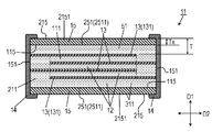
- FIG. 1 is a perspective view of a laminated varistor according to an embodiment.
- FIG. 2 is a cross-sectional view taken along the line II-II of the laminated varistor shown in FIG.
- FIG. 3 is a cross-sectional view taken along the line III-III of the laminated varistor shown in FIG.
- FIG. 4 is an enlarged cross-sectional view of the laminated varistor shown in FIG.
- FIG. 1 is a perspective view of the laminated varistor 11 in the embodiment.
- FIG. 2 is a cross-sectional view taken along the line II-II of the laminated varistor 11 shown in FIG.
- FIG. 3 is a cross-sectional view taken along the line III-III of the laminated varistor 11 shown in FIG.
- the laminated varistor 11 includes a sintered body 51, a pair of external electrodes 14 provided on each of the pair of end faces 151 of the sintered body 51, and a high resistance layer 15 provided on the surface 251 of the sintered body 51. ..
- the sintered body 51 has a plurality of varistor layers 12 containing ZnO as a main component, and a plurality of internal electrodes 13 containing Ag as a main component, which are alternately laminated with a plurality of varistor layers 12 in the stacking direction D1.
- the internal electrode 13 is embedded in the sintered body 51.
- the plurality of internal electrodes 13 are alternately led out to both end faces on opposite sides of the sintered body 51, and are electrically connected to the pair of external electrodes 14 on both end faces 151.
- the sintered body 51 of the laminated varistor 11 in the embodiment has a pair of end faces 151 having rectangular shapes on opposite sides, a pair of surfaces 2511 having rectangular shapes on opposite sides, and a rectangular shape on opposite sides.
- the internal electrode 13 is derived from the end face 151.
- the plurality of internal electrodes 13 are arranged in the stacking direction D1.
- a pair of internal electrodes 131 located at the outermost edges of the plurality of internal electrodes 13 arranged in the stacking direction D1 are led out to a pair of end faces 151.
- the sintered body 51 has a pair of end faces 151 from which the pair of internal electrodes 131 (13) are derived, and a surface 251 on which the pair of internal electrodes 131 (13) excluding the pair of end faces 151 are not exposed. And have.
- Surface 251 includes surfaces 2511 and 2512.
- the sintered body 51 (laminated varistor 11) has an effective portion 111 sandwiched between a pair of internal electrodes 131 and an invalid portion 211 surrounding the effective portion 111.
- the effective portion 111 functions as a varistor, and the invalid portion 211 does not function as a varistor.
- the thickness of the high resistance layer 15 is about 100 ⁇ m.
- the invalid portion 211 of the sintered body 51 and the high resistance layer 15 form an invalid portion 311 surrounding the effective portion 111 of the laminated varistor 11.
- the invalid part 311 does not function as a varistor.
- FIG. 4 is an enlarged cross-sectional view of the laminated varistor 11.
- a plating layer 141 made of Sn and Ni is formed on the outer surface of the external electrode 14.
- the varistor layer 12 laminated between the internal electrodes 13 and the outer side thereof contains ZnO as a main component, and further contains subcomponents such as Bi 2 O 3 , Co 2 O 3 , MnO 2 , or Sb 2 O 3 . ..
- the composition contains only 1.0 mol% of Bi 2 O 3 and 2.0 mol% of other subcomponents such as Co 2 O 3 , Mn O 2 and Sb 2 O 3 , and ZnO. Is contained only in the remaining 97 mol%.
- the high resistance layer 15 has an inner surface 115 facing the sintered body 51 and an outer surface 215 on the opposite side of the inner surface 115.
- the surface layer portion 2151 of the high resistance layer 15 near the outer surface including the outer surface 215 contains Zn, Si, and Bi, and in the embodiment, contains Zn 2 SiO 4 as a main component.
- the high resistivity layer 15 has a resistivity much higher than the resistivity of the effective portion 111 between the internal electrodes 13 of the sintered body 51.
- As the composition of the high resistance layer 15 only 58.2 mol% of Zn is contained, only 38.8 mol% of Si is contained, and only 3.0 mol% of Bi is contained.
- the specific resistance of the sintered body 11 between the internal electrodes 13 is four times as large as the surface 251 excluding the end surface 151 from which the internal electrode 13 is derived, that is, the four surfaces 2511 and 2512.
- the high resistance layer 15 having the above specific resistance is provided with a thickness of 50 ⁇ m or more. As a result, sufficient insulation can be achieved, and the external electrode 14 can be stably plated to form the plating layer 141.
- the space between the internal electrode 131 (13) and the high resistance layer 15 is composed of a varistor layer having the same composition as the sintered body 51 (varistor layer 12) of the effective portion 111 sandwiched between the internal electrodes 13. If the Si of the high resistance layer 15 diffuses into the varistor layer 12 of the effective portion 111 sandwiched between the internal electrodes 13, the resistance value increases.
- the ineffective portion 211 between the effective portion 111 and the high resistance layer 15 prevents the Si of the high resistance layer 15 from diffusing into the effective portion 111, and prevents the effective portion 111, that is, the resistance value of the laminated varistor 11 from increasing.
- the thickness of the invalid portion 211 is about 300 ⁇ m.
- the thickness T of the invalid portion 311 of the outer surface 215 and the thickness Tx of the high resistance layer 15 are 0.1 ⁇ (Tx / T) ⁇ 0.8 with respect to the internal electrode 131 (13). It is desirable to satisfy the relationship. If the value of (Tx / T) is smaller than 0.1, it becomes difficult to secure sufficient insulation, and conversely, if it is larger than 0.8, the characteristics may be affected by diffusion. is there.
- the distance W from the end of the internal electrode 13 to the outer surface 215 of the high resistance layer 15 and the thickness Wx of the high resistance layer 15 are 0.1 ⁇ (Wx / W) ⁇ 0. It is desirable to satisfy the relationship of 8.
- the surface layer portion 2151 of the high resistance layer 15 contains at least Zn, Bi, and Si.
- the Bi content of the surface layer portion 2151 is twice or more and five times or less the Bi content of the varistor layer 12. It is desirable that the atomic ratio Ra of Zn to Si satisfies 1.0 ⁇ Ra ⁇ 2.0. When Zn and Si react to form Zn 2 SiO 4 , Bi 2 O 3 acts as a reaction accelerator to promote this reaction. If the Bi content of the high resistance layer 15 is less than twice the Bi content of the varistor layer 12, Bi may move from the varistor layer 12 and the non-linearity of the varistor may deteriorate.
- the Bi content of the high resistance layer 15 is more than 5 times the Bi content of the varistor layer 12, the difference in shrinkage between the high resistance layer 15 and the varistor layer 12 becomes large, and the varistor layer 12 and the varistor layer 12 are high. Peeling, cracks, etc. may occur between the resistance layers 15.
- the atomic ratio Ra becomes larger than 2.0, the insulation resistance of the high resistance layer 15 deteriorates due to the excess ZnO.
- the atomic ratio Ra is smaller than 1.0, there is a possibility that problems such as fusion of elements during firing may occur due to the surplus SiO 2 .
- the high resistance layer 15 contains Si.
- the high resistance layer 15 may contain Sb instead of Si.
- the surface layer portion 2151 of the high resistance layer 15 contains at least Zn, Bi, and Sb, and the Bi content of the surface layer portion 2151 of the high resistance layer 15 is twice or more and five times the Bi content of the varistor layer 12. It is as follows. It is desirable that the atomic ratio Rb of Zn to Sb satisfies 3.5 ⁇ Rb ⁇ 7.0. In this case as well, as with Si, when Zn and Sb react to form Zn 7 Sb 2 O 12 , Bi 2 O 3 acts as a reaction accelerator to promote this reaction.
- a slurry of a high resistance material which is a material of the high resistance layer 15, is prepared.
- the blending ratio of this slurry is that the ZnO content is 58.2 mol%, the SiO 2 content is 38.8 mol%, and the Bi 2 O 3 content is 3.0 mol%.
- a slurry of the varistor material which is the material of the varistor layer 12 is prepared.
- the blending ratio of this slurry is that the content of Bi 2 O 3 is 1.0 mol%, and the content of auxiliary components containing Co 2 O 3 , MnO 2 , Sb 2 O 3, etc. is 2.0 mol%. , ZnO content is the remaining 97 mol%.
- a slurry of high resistance material is applied and dried on a carrier film and transferred onto a carrier plate to form a high resistance green sheet having a thickness of about 100 ⁇ m.
- a high resistance material formed in a pattern having a width of about 200 ⁇ m is laminated on the high resistance green sheet so as to be a portion of the high resistance layer 15 located on the surface 2512 of the sintered body 51 so as to have a height of about 300 ⁇ m. To do. By being divided at the center of this pattern, the width of the high resistance layer 15 on the surface 2512 of the sintered body 51 becomes about 100 ⁇ m.
- the varistor material is laminated between the pattern-formed high resistance materials.
- a high resistance material with a pattern formed on it and a varistor material with an internal electrode material printed between them are laminated.
- a pattern-formed high resistance material and a varistor material are laminated between them, and a high resistance material is laminated on the high resistance material to form a laminate.
- the laminate is pressed to cut it into pieces, and then fired.
- the end face 151 of the sintered body 51 with the internal electrode 13 exposed is coated with a paste containing Ag as a main component and baked, and the external electrode 14 (lower) It forms a stratum 142).
- the plating layer 141 is formed by plating Sn and Ni on the external electrode 14 (base layer 142) to obtain the laminated varistor 11.
- the portion of the sintered body 11 other than the portion where the external electrode 14 is provided is entirely covered with the high resistance layer 15 having a thickness of 50 ⁇ m or more. That is, the sintered body 51 is entirely covered with the external electrode 14 and the high resistance layer 15 so as not to be exposed to the outside of the laminated varistor 11. Therefore, the external electrode 14 can be stably plated.
- the high resistance layer can be formed by applying a high resistance paste to the surface of the varistor element and baking it, but it takes a lot of man-hours and the varistor becomes expensive. In addition, the thickness of the high resistance layer tends to vary, which tends to cause plating defects in the external electrodes. Further, since the high resistance paste is applied and baked on the six surfaces of the varistor element, a part of the components of the high resistance paste is diffused inside the varistor element from the surface from which the internal electrode is derived, and the specific resistance of the varistor layer is increased. The surge resistance may be reduced.
- the laminated varistor 11 does not require a special step of forming the high resistance layer 15 such as a glass coating, and since the sheet-like materials are laminated to form the high resistance layer 15, the thickness and the thickness and the thickness of the laminated varistor 11 are increased.
- the width can be formed with high accuracy. Further, since it is possible to prevent the diffusion of the components of the high resistance layer from the end face from which the internal electrode 13 is led out, it is possible to obtain a laminated varistor 11 which is inexpensive, has excellent surge resistance, and can apply stable plating to the external electrode 14. Can be done.
Landscapes
- Engineering & Computer Science (AREA)
- Microelectronics & Electronic Packaging (AREA)
- Physics & Mathematics (AREA)
- Electromagnetism (AREA)
- Thermistors And Varistors (AREA)
Abstract
La présente invention porte sur une varistance stratifiée qui est pourvue d'un corps fritté, d'une paire d'électrodes externes disposées sur le corps fritté, et d'une couche à haute résistivité disposée sur le corps fritté. Le corps fritté comporte une couche de varistance qui contient du Bi et du ZnO en tant que constituant principal, et une paire d'électrodes internes qui sont incorporées dans la couche de varistance. Le corps fritté présente une paire de faces d'extrémité d'où est extraite la paire d'électrodes internes, respectivement, et une surface autre que la paire de faces d'extrémité, où la paire d'électrodes internes n'est pas mise à nu. La paire d'électrodes externes est respectivement disposée sur la paire de faces d'extrémité du corps fritté et électriquement connectée à la paire d'électrodes internes, respectivement. La couche à haute résistivité est disposée sur la surface où la paire d'électrodes internes n'est pas mise à nu, présente une résistance spécifique qui est supérieure ou égale à quatre fois la résistance spécifique d'une partie de la couche de varistance située entre la paire d'électrodes internes, et présente une épaisseur d'au moins 50 µm. Cette varistance stratifiée peut être rendue compacte tout en offrant d'excellentes caractéristiques anti-surtension, et permet également un placage stable d'électrodes externes.
Priority Applications (1)
| Application Number | Priority Date | Filing Date | Title |
|---|---|---|---|
| JP2021508701A JPWO2020194812A1 (fr) | 2019-03-22 | 2019-10-16 |
Applications Claiming Priority (2)
| Application Number | Priority Date | Filing Date | Title |
|---|---|---|---|
| JP2019-053995 | 2019-03-22 | ||
| JP2019053995 | 2019-03-22 |
Publications (1)
| Publication Number | Publication Date |
|---|---|
| WO2020194812A1 true WO2020194812A1 (fr) | 2020-10-01 |
Family
ID=72610755
Family Applications (1)
| Application Number | Title | Priority Date | Filing Date |
|---|---|---|---|
| PCT/JP2019/040562 Ceased WO2020194812A1 (fr) | 2019-03-22 | 2019-10-16 | Varistance stratifiée |
Country Status (2)
| Country | Link |
|---|---|
| JP (1) | JPWO2020194812A1 (fr) |
| WO (1) | WO2020194812A1 (fr) |
Cited By (3)
| Publication number | Priority date | Publication date | Assignee | Title |
|---|---|---|---|---|
| US11276515B2 (en) * | 2019-02-22 | 2022-03-15 | Panasonic Intellectual Property Management Co., Ltd. | Varistor and method for producing same |
| JP2023035178A (ja) * | 2021-08-31 | 2023-03-13 | パナソニックIpマネジメント株式会社 | バリスタ及びその製造方法 |
| US11935675B2 (en) * | 2022-07-04 | 2024-03-19 | Yageo Corporation | Anti-surge resistor and fabrication method thereof |
Citations (3)
| Publication number | Priority date | Publication date | Assignee | Title |
|---|---|---|---|---|
| JPS6060702A (ja) * | 1983-09-13 | 1985-04-08 | マルコン電子株式会社 | 積層型電圧非直線抵抗器 |
| JPH01295403A (ja) * | 1988-01-27 | 1989-11-29 | Murata Mfg Co Ltd | チップバリスタ |
| JPH11233309A (ja) * | 1998-02-10 | 1999-08-27 | Murata Mfg Co Ltd | 積層バリスタ |
-
2019
- 2019-10-16 JP JP2021508701A patent/JPWO2020194812A1/ja active Pending
- 2019-10-16 WO PCT/JP2019/040562 patent/WO2020194812A1/fr not_active Ceased
Patent Citations (3)
| Publication number | Priority date | Publication date | Assignee | Title |
|---|---|---|---|---|
| JPS6060702A (ja) * | 1983-09-13 | 1985-04-08 | マルコン電子株式会社 | 積層型電圧非直線抵抗器 |
| JPH01295403A (ja) * | 1988-01-27 | 1989-11-29 | Murata Mfg Co Ltd | チップバリスタ |
| JPH11233309A (ja) * | 1998-02-10 | 1999-08-27 | Murata Mfg Co Ltd | 積層バリスタ |
Cited By (4)
| Publication number | Priority date | Publication date | Assignee | Title |
|---|---|---|---|---|
| US11276515B2 (en) * | 2019-02-22 | 2022-03-15 | Panasonic Intellectual Property Management Co., Ltd. | Varistor and method for producing same |
| JP2023035178A (ja) * | 2021-08-31 | 2023-03-13 | パナソニックIpマネジメント株式会社 | バリスタ及びその製造方法 |
| JP7724470B2 (ja) | 2021-08-31 | 2025-08-18 | パナソニックIpマネジメント株式会社 | バリスタ及びその製造方法 |
| US11935675B2 (en) * | 2022-07-04 | 2024-03-19 | Yageo Corporation | Anti-surge resistor and fabrication method thereof |
Also Published As
| Publication number | Publication date |
|---|---|
| JPWO2020194812A1 (fr) | 2020-10-01 |
Similar Documents
| Publication | Publication Date | Title |
|---|---|---|
| JPH04333295A (ja) | 電歪効果素子およびその製造方法 | |
| WO2020194812A1 (fr) | Varistance stratifiée | |
| JP2019067793A (ja) | 電子部品 | |
| JPH02135702A (ja) | 積層型バリスタ | |
| JP4840392B2 (ja) | 積層コンデンサ | |
| JP4074299B2 (ja) | 積層型チップバリスタ | |
| WO2016139975A1 (fr) | Thermistance ctn à enrober dans un substrat et son procédé de production | |
| JPWO2019073762A1 (ja) | 積層電子部品の製造方法 | |
| US7705708B2 (en) | Varistor and method of producing the same | |
| JPH02189903A (ja) | 積層型バリスタ | |
| JP2007165639A (ja) | バリスタ及びバリスタの製造方法 | |
| JP3981125B2 (ja) | 積層型チップバリスタ及びその製造方法 | |
| JP4907138B2 (ja) | チップ型ntc素子 | |
| US20240212892A1 (en) | Laminated ceramic component | |
| JP7300589B2 (ja) | 積層バリスタの製造方法および積層バリスタ | |
| JPH06260302A (ja) | チップ型ptcサーミスタ | |
| JP2995829B2 (ja) | 磁性体内蔵型回路基板 | |
| JP4276231B2 (ja) | バリスタ素子 | |
| JP2019179812A (ja) | 積層バリスタの製造方法 | |
| JP2002252385A (ja) | 積層圧電アクチュエータ素子 | |
| JP4127696B2 (ja) | バリスタ及びその製造方法 | |
| JPH0273604A (ja) | 積層型バリスタ | |
| JPH03222302A (ja) | 可変積層バリスタ | |
| JP2006269993A (ja) | 積層型チップバリスタ及びその製造方法 | |
| JPH0273602A (ja) | 積層型バリスタ |
Legal Events
| Date | Code | Title | Description |
|---|---|---|---|
| 121 | Ep: the epo has been informed by wipo that ep was designated in this application |
Ref document number: 19920760 Country of ref document: EP Kind code of ref document: A1 |
|
| ENP | Entry into the national phase |
Ref document number: 2021508701 Country of ref document: JP Kind code of ref document: A |
|
| NENP | Non-entry into the national phase |
Ref country code: DE |
|
| 122 | Ep: pct application non-entry in european phase |
Ref document number: 19920760 Country of ref document: EP Kind code of ref document: A1 |