WO2021060118A1 - 撮像装置 - Google Patents
撮像装置 Download PDFInfo
- Publication number
- WO2021060118A1 WO2021060118A1 PCT/JP2020/035144 JP2020035144W WO2021060118A1 WO 2021060118 A1 WO2021060118 A1 WO 2021060118A1 JP 2020035144 W JP2020035144 W JP 2020035144W WO 2021060118 A1 WO2021060118 A1 WO 2021060118A1
- Authority
- WO
- WIPO (PCT)
- Prior art keywords
- pixel
- unit
- wavelength region
- region
- pixels
- Prior art date
- Legal status (The legal status is an assumption and is not a legal conclusion. Google has not performed a legal analysis and makes no representation as to the accuracy of the status listed.)
- Ceased
Links
Images


Classifications
-
- H—ELECTRICITY
- H10—SEMICONDUCTOR DEVICES; ELECTRIC SOLID-STATE DEVICES NOT OTHERWISE PROVIDED FOR
- H10F—INORGANIC SEMICONDUCTOR DEVICES SENSITIVE TO INFRARED RADIATION, LIGHT, ELECTROMAGNETIC RADIATION OF SHORTER WAVELENGTH OR CORPUSCULAR RADIATION
- H10F39/00—Integrated devices, or assemblies of multiple devices, comprising at least one element covered by group H10F30/00, e.g. radiation detectors comprising photodiode arrays
- H10F39/80—Constructional details of image sensors
- H10F39/805—Coatings
- H10F39/8053—Colour filters
-
- H—ELECTRICITY
- H04—ELECTRIC COMMUNICATION TECHNIQUE
- H04N—PICTORIAL COMMUNICATION, e.g. TELEVISION
- H04N25/00—Circuitry of solid-state image sensors [SSIS]; Control thereof
- H04N25/10—Circuitry of solid-state image sensors [SSIS]; Control thereof for transforming different wavelengths into image signals
- H04N25/11—Arrangement of colour filter arrays [CFA]; Filter mosaics
- H04N25/13—Arrangement of colour filter arrays [CFA]; Filter mosaics characterised by the spectral characteristics of the filter elements
- H04N25/134—Arrangement of colour filter arrays [CFA]; Filter mosaics characterised by the spectral characteristics of the filter elements based on three different wavelength filter elements
-
- H—ELECTRICITY
- H04—ELECTRIC COMMUNICATION TECHNIQUE
- H04N—PICTORIAL COMMUNICATION, e.g. TELEVISION
- H04N25/00—Circuitry of solid-state image sensors [SSIS]; Control thereof
- H04N25/60—Noise processing, e.g. detecting, correcting, reducing or removing noise
- H04N25/61—Noise processing, e.g. detecting, correcting, reducing or removing noise the noise originating only from the lens unit, e.g. flare, shading, vignetting or "cos4"
- H04N25/615—Noise processing, e.g. detecting, correcting, reducing or removing noise the noise originating only from the lens unit, e.g. flare, shading, vignetting or "cos4" involving a transfer function modelling the optical system, e.g. optical transfer function [OTF], phase transfer function [PhTF] or modulation transfer function [MTF]
- H04N25/6153—Noise processing, e.g. detecting, correcting, reducing or removing noise the noise originating only from the lens unit, e.g. flare, shading, vignetting or "cos4" involving a transfer function modelling the optical system, e.g. optical transfer function [OTF], phase transfer function [PhTF] or modulation transfer function [MTF] for colour signals
-
- G—PHYSICS
- G02—OPTICS
- G02B—OPTICAL ELEMENTS, SYSTEMS OR APPARATUS
- G02B5/00—Optical elements other than lenses
- G02B5/20—Filters
- G02B5/201—Filters in the form of arrays
-
- H—ELECTRICITY
- H04—ELECTRIC COMMUNICATION TECHNIQUE
- H04N—PICTORIAL COMMUNICATION, e.g. TELEVISION
- H04N23/00—Cameras or camera modules comprising electronic image sensors; Control thereof
- H04N23/80—Camera processing pipelines; Components thereof
- H04N23/84—Camera processing pipelines; Components thereof for processing colour signals
-
- H—ELECTRICITY
- H04—ELECTRIC COMMUNICATION TECHNIQUE
- H04N—PICTORIAL COMMUNICATION, e.g. TELEVISION
- H04N25/00—Circuitry of solid-state image sensors [SSIS]; Control thereof
- H04N25/10—Circuitry of solid-state image sensors [SSIS]; Control thereof for transforming different wavelengths into image signals
- H04N25/11—Arrangement of colour filter arrays [CFA]; Filter mosaics
- H04N25/13—Arrangement of colour filter arrays [CFA]; Filter mosaics characterised by the spectral characteristics of the filter elements
- H04N25/131—Arrangement of colour filter arrays [CFA]; Filter mosaics characterised by the spectral characteristics of the filter elements including elements passing infrared wavelengths
-
- H—ELECTRICITY
- H04—ELECTRIC COMMUNICATION TECHNIQUE
- H04N—PICTORIAL COMMUNICATION, e.g. TELEVISION
- H04N25/00—Circuitry of solid-state image sensors [SSIS]; Control thereof
- H04N25/10—Circuitry of solid-state image sensors [SSIS]; Control thereof for transforming different wavelengths into image signals
- H04N25/11—Arrangement of colour filter arrays [CFA]; Filter mosaics
- H04N25/13—Arrangement of colour filter arrays [CFA]; Filter mosaics characterised by the spectral characteristics of the filter elements
- H04N25/133—Arrangement of colour filter arrays [CFA]; Filter mosaics characterised by the spectral characteristics of the filter elements including elements passing panchromatic light, e.g. filters passing white light
-
- H—ELECTRICITY
- H04—ELECTRIC COMMUNICATION TECHNIQUE
- H04N—PICTORIAL COMMUNICATION, e.g. TELEVISION
- H04N25/00—Circuitry of solid-state image sensors [SSIS]; Control thereof
- H04N25/10—Circuitry of solid-state image sensors [SSIS]; Control thereof for transforming different wavelengths into image signals
- H04N25/11—Arrangement of colour filter arrays [CFA]; Filter mosaics
- H04N25/13—Arrangement of colour filter arrays [CFA]; Filter mosaics characterised by the spectral characteristics of the filter elements
- H04N25/135—Arrangement of colour filter arrays [CFA]; Filter mosaics characterised by the spectral characteristics of the filter elements based on four or more different wavelength filter elements
-
- H—ELECTRICITY
- H04—ELECTRIC COMMUNICATION TECHNIQUE
- H04N—PICTORIAL COMMUNICATION, e.g. TELEVISION
- H04N25/00—Circuitry of solid-state image sensors [SSIS]; Control thereof
- H04N25/40—Extracting pixel data from image sensors by controlling scanning circuits, e.g. by modifying the number of pixels sampled or to be sampled
- H04N25/46—Extracting pixel data from image sensors by controlling scanning circuits, e.g. by modifying the number of pixels sampled or to be sampled by combining or binning pixels
-
- H—ELECTRICITY
- H04—ELECTRIC COMMUNICATION TECHNIQUE
- H04N—PICTORIAL COMMUNICATION, e.g. TELEVISION
- H04N25/00—Circuitry of solid-state image sensors [SSIS]; Control thereof
- H04N25/70—SSIS architectures; Circuits associated therewith
-
- H—ELECTRICITY
- H04—ELECTRIC COMMUNICATION TECHNIQUE
- H04N—PICTORIAL COMMUNICATION, e.g. TELEVISION
- H04N25/00—Circuitry of solid-state image sensors [SSIS]; Control thereof
- H04N25/70—SSIS architectures; Circuits associated therewith
- H04N25/76—Addressed sensors, e.g. MOS or CMOS sensors
- H04N25/78—Readout circuits for addressed sensors, e.g. output amplifiers or A/D converters
-
- H—ELECTRICITY
- H10—SEMICONDUCTOR DEVICES; ELECTRIC SOLID-STATE DEVICES NOT OTHERWISE PROVIDED FOR
- H10F—INORGANIC SEMICONDUCTOR DEVICES SENSITIVE TO INFRARED RADIATION, LIGHT, ELECTROMAGNETIC RADIATION OF SHORTER WAVELENGTH OR CORPUSCULAR RADIATION
- H10F39/00—Integrated devices, or assemblies of multiple devices, comprising at least one element covered by group H10F30/00, e.g. radiation detectors comprising photodiode arrays
- H10F39/80—Constructional details of image sensors
- H10F39/802—Geometry or disposition of elements in pixels, e.g. address-lines or gate electrodes
-
- G—PHYSICS
- G02—OPTICS
- G02B—OPTICAL ELEMENTS, SYSTEMS OR APPARATUS
- G02B5/00—Optical elements other than lenses
- G02B5/20—Filters
- G02B5/208—Filters for use with infrared or ultraviolet radiation, e.g. for separating visible light from infrared and/or ultraviolet radiation
Definitions
- This disclosure relates to an imaging device.
- a color filter for each color of R (red), G (green), and B (blue) and a filter for transmitting light in substantially the entire visible light region (called a W color (white) color filter) were used.
- Two-dimensional image sensors are known.
- pixels provided with a W color filter are arranged every other in the vertical and horizontal directions of the block, in units of a pixel block of 4 pixels ⁇ 4 pixels. Will be done. Further, two pixels provided with an R color filter, two pixels provided with a B color filter, and four pixels provided with a G color filter have the same color filter. The provided pixels are arranged so as not to come into contact with each other in an oblique direction.
- Such a two-dimensional image sensor using the R, G, and B color filters and the W color filter obtains a full-color image based on the light transmitted through the R, G, and B color filters. At the same time, high sensitivity can be obtained based on the light transmitted through the W color filter. Further, such a two-dimensional image sensor is expected to be used as a surveillance camera or an in-vehicle camera because it can separate a visible image and an IR (Infrared) image by signal processing.
- IR Infrared
- An object of the present disclosure is to provide an imaging device capable of improving the quality of an image captured by using a color filter.
- the imaging apparatus includes a pixel array including pixels arranged in a matrix arrangement, the pixel array has a plurality of pixel blocks each containing 6 ⁇ 6 pixels, and the pixel block is a pixel block.
- a first pixel provided with a first optical filter that transmits light in the first wavelength region, and a second pixel provided with a second optical filter that transmits light in the second wavelength region.
- a third pixel provided with a third optical filter that transmits light in the third wavelength region, and a fourth pixel provided with a fourth optical filter that transmits light in the fourth wavelength region.
- the first pixel is arranged every other row and column direction of the array, and each row and each column of the array has a second pixel, a third pixel, and a fourth pixel, respectively. Pixels are arranged one by one, and the pixel block further arranges the second pixel, the third pixel, and the fourth pixel in the first diagonal direction of the arrangement, which is parallel to the diagonal of the pixel block. Includes a sequence containing at least one pixel block and a sequence containing at least one pixel block in a second diagonal direction parallel to the diagonal of the pixel block and different from the first diagonal direction.
- the color filters of the R (red), G (green), and B (blue) colors selectively transmit light in the red wavelength region, the green wavelength region, and the blue wavelength region, respectively. It is a filter.
- the W (white) color filter is, for example, an optical filter that transmits light in a wavelength region of substantially the entire range of visible light at a predetermined transmittance or higher.
- Selectively transmitting light in a certain wavelength region means that light in the wavelength region is transmitted at a predetermined transmittance or higher, and a wavelength region other than the wavelength region is transmitted at a transmittance less than the predetermined transmittance. It shall mean that.
- FIG. 1 is a functional block diagram of an example for explaining the function of the image pickup apparatus applicable to the first embodiment.
- the image pickup apparatus 1 includes an image pickup unit 10, an optical unit 11, an image processing unit 12, an output processing unit 13, and a control unit 14.
- the imaging unit 10 has a pixel array in which a plurality of pixels including one or more light receiving elements are arranged in a matrix.
- an optical filter color filter
- the optical unit 11 includes a lens, an aperture mechanism, a focus mechanism, and the like, and guides the light from the subject to the light receiving surface of the pixel array.
- the imaging unit 10 reads a pixel signal from each pixel exposed at a specified exposure time, performs signal processing such as noise removal and gain adjustment on the read pixel signal, and converts the read pixel signal into digital pixel data.
- the imaging unit 10 outputs pixel data based on this pixel signal.
- a series of operations by the imaging unit 10 to read pixel signals from exposed pixels and exposed pixels and output them as pixel data is called imaging.
- the image processing unit 12 performs predetermined signal processing on the pixel data output from the imaging unit 10 and outputs the data.
- the signal processing performed by the image processing unit 12 on the pixel data is, for example, on the pixel data of each pixel provided with color filters of each color of R (red), G (green), and B (blue) on a one-to-one basis. Includes simultaneous processing to have information on each color of R, G, and B.
- the image processing unit 12 outputs each pixel data that has undergone signal processing.
- the output processing unit 13 outputs the image data output from the image processing unit 12 as, for example, frame-based image data. At this time, the output processing unit 13 converts the output image data into a format suitable for output from the image pickup apparatus 1.
- the output image data output from the output processing unit 13 is supplied to, for example, a display (not shown) and displayed as an image. Not limited to this, the output image data may be supplied to another device, for example, a device that performs recognition processing on the output image data, or a control device that controls based on the output image data.
- the control unit 14 controls the overall operation of the image pickup device 1.
- the control unit 14 includes, for example, a CPU (Central Processing Unit) and an interface circuit for communicating with each unit of the image pickup apparatus 1, and the CPU generates and generates various control signals by operating according to a predetermined program. Each part of the image pickup apparatus 1 is controlled by the control signal.
- a CPU Central Processing Unit
- the image processing unit 12 and the output processing unit 13 described above can be configured by, for example, a DSP (Digital Signal Processor) or an ISP (Image Signal Processor) that operates according to a predetermined program.
- a DSP Digital Signal Processor
- ISP Image Signal Processor
- one or both of the image processing unit 12 and the output processing unit 13 may be realized by a program that operates on the CPU together with the control unit 14. These programs may be stored in advance in the non-volatile memory of the image pickup apparatus 1, or may be supplied to the image pickup apparatus 1 from the outside and written to the memory.
- FIG. 2 is a block diagram showing a configuration of an example of the imaging unit 10 applicable to each embodiment.
- the imaging unit 10 includes a pixel array unit 110, a vertical scanning unit 20, a horizontal scanning unit 21, and a control unit 22.
- the pixel array unit 110 includes a plurality of pixels 100 each having a light receiving element that generates a voltage corresponding to the received light.
- a photodiode can be used as the light receiving element.
- the plurality of pixels 100 are arranged in a matrix in the horizontal direction (row direction) and the vertical direction (column direction).
- the arrangement of the pixels 100 in the row direction is called a line.
- An image (image data) of one frame is formed based on the pixel signals read from a predetermined number of lines in the pixel array unit 110. For example, when an image of one frame is formed by 3000 pixels ⁇ 2000 lines, the pixel array unit 110 includes at least 2000 lines including at least 3000 pixels 100.
- a pixel signal line HCTL is connected to each row and column of each pixel 100, and a vertical signal line VSL is connected to each column.
- the end portion of the pixel signal line HCTL that is not connected to the pixel array unit 110 is connected to the vertical scanning unit 20.
- the vertical scanning unit 20 transmits a plurality of control signals such as a drive pulse when reading a pixel signal from the pixel 100 to the pixel array unit 110 via the pixel signal line HCTL according to the control signal supplied from the control unit 14, for example. To do.
- the end of the vertical signal line VSL that is not connected to the pixel array unit 110 is connected to the horizontal scanning unit 21.
- the horizontal scanning unit 21 includes an AD (Analog to Digital) conversion unit, an output unit, and a signal processing unit.
- the pixel signal read from the pixel 100 is transmitted to the AD conversion unit of the horizontal scanning unit 21 via the vertical signal line VSL.
- the reading control of the pixel signal from the pixel 100 will be schematically described.
- the pixel signal from the pixel 100 is read out by transferring the electric charge accumulated in the light receiving element by exposure to the floating diffusion layer (FD) and converting the electric charge transferred in the floating diffusion layer into a voltage.
- the voltage at which the charge is converted in the floating diffusion layer is output to the vertical signal line VSL via an amplifier.
- the space between the light receiving element and the floating diffusion layer is set to an off (open) state, and in the light receiving element, the electric charge generated according to the light incident by the photoelectric conversion is generated. Accumulate.
- the floating diffusion layer and the vertical signal line VSL are connected according to the selection signal supplied via the pixel signal line HCTL. Further, the floating diffusion layer is connected to the supply line of the power supply voltage VDD or the black level voltage in a short period of time according to the reset pulse supplied via the pixel signal line HCTL to reset the floating diffusion layer.
- a voltage (referred to as voltage P) at the reset level of the floating diffusion layer is output to the vertical signal line VSL.
- the transfer pulse supplied via the pixel signal line HCTL puts the light receiving element and the floating diffusion layer on (closed), and transfers the electric charge accumulated in the light receiving element to the floating diffusion layer.
- a voltage (referred to as voltage Q) corresponding to the amount of electric charge of the floating diffusion layer is output to the vertical signal line VSL.
- the AD conversion unit includes an AD converter provided for each vertical signal line VSL, and the pixel signal supplied from the pixel 100 via the vertical signal line VSL is subjected to AD conversion processing by the AD converter. Is applied, and two digital values (values corresponding to voltage P and voltage Q, respectively) for correlated double sampling (CDS: Correlated Double Sampling) processing for noise reduction are generated.
- CDS Correlated Double Sampling
- the two digital values generated by the AD converter are subjected to CDS processing by the signal processing unit, and a pixel signal (pixel data) based on the digital signal is generated.
- the generated pixel data is output from the imaging unit 10.
- the horizontal scanning unit 21 performs selective scanning for selecting the AD converters for each vertical signal line VSL in a predetermined order, so that each AD converter temporarily holds the AD converters. Digital values are sequentially output to the signal processing unit.
- the horizontal scanning unit 21 realizes this operation by a configuration including, for example, a shift register and an address decoder.
- the control unit 22 controls the drive of the vertical scanning unit 20, the horizontal scanning unit 21, and the like.
- the control unit 22 generates various drive signals that serve as a reference for the operation of the vertical scanning unit 20 and the horizontal scanning unit 21.
- the control unit 22 supplies the vertical scanning unit 20 to each pixel 100 via the pixel signal line HCTL based on the vertical synchronization signal or the external trigger signal supplied from the outside (for example, the control unit 14) and the horizontal synchronization signal. To generate a control signal for.
- the control unit 22 supplies the generated control signal to the vertical scanning unit 20.
- the vertical scanning unit 20 Based on the control signal supplied from the control unit 22, the vertical scanning unit 20 supplies various signals including drive pulses to the pixel signal line HCTL of the selected pixel line of the pixel array unit 110 to each pixel 100 for each line. Then, the pixel signal is output from each pixel 100 to the vertical signal line VSL.
- the vertical scanning unit 20 is configured by using, for example, a shift register or an address decoder.
- the imaging unit 10 configured in this way is a column AD type CMOS (Complementary Metal Oxide Semiconductor) image sensor in which AD converters are arranged for each column.
- CMOS Complementary Metal Oxide Semiconductor
- FIG. 3 is a block diagram showing an example of the hardware configuration of the image pickup apparatus 1 applicable to the first embodiment.
- the image pickup apparatus 1 is connected to the CPU 2000 by the bus 2020, respectively, the CPU 2000, the ROM (Read Only Memory) 2001, the RAM (Random Access Memory) 2002, the image pickup unit 2003, the storage 2004, and the data I / The F2005, the operation unit 2006, and the display control unit 2007 are included.
- the image pickup apparatus 1 includes an image processing unit 2010 and an output I / F 2012, each of which is connected by a bus 2020.
- the CPU 2000 controls the overall operation of the image pickup apparatus 1 by using the RAM 2002 as a work memory according to a program stored in the ROM 2001 in advance.
- the imaging unit 2003 corresponds to the imaging unit 10 of FIG. 1, performs imaging, and outputs pixel data.
- the pixel data output from the image pickup unit 2003 is supplied to the image processing unit 2010.
- the image processing unit 2010 corresponds to the image processing unit 12 of FIG. 1 and includes a part of the functions of the output processing unit 13.
- the image processing unit 2010 performs predetermined signal processing on the pixel data supplied from the imaging unit 10 and sequentially writes the pixel data to the frame memory 2011.
- the pixel data for one frame written in the frame memory 2011 is output from the image processing unit 2010 as image data for each frame.
- the output I / F 2012 is an interface for outputting the image data output from the image processing unit 2010 to the outside.
- the output I / F 2012 includes, for example, a part of the functions of the output processing unit 13 of FIG. 1, and can convert the image data supplied from the image processing unit 2010 into image data of a predetermined format and output it.
- the storage 2004 is, for example, a flash memory, and can store and store image data output from the image processing unit 2010.
- the storage 2004 can also store a program for operating the CPU 2000.
- the storage 2004 is not limited to the configuration built in the image pickup device 1, and may be a structure that can be attached to and detached from the image pickup device 1.
- the data I / F 2005 is an interface for the imaging device 1 to send and receive data to and from an external device.
- USB Universal Serial Bus
- the data I / F2005 for example, USB (Universal Serial Bus) can be applied.
- an interface for performing short-range wireless communication such as Bluetooth (registered trademark) can also be applied.
- the operation unit 2006 accepts user operations on the image pickup device 1.
- the operation unit 2006 includes an operator such as a dial or a button as an input device that accepts user input.
- the operation unit 2006 may include a touch panel as an input device that outputs a signal according to the contact position.
- the display control unit 2007 generates a display signal that can be displayed by the display 2008 based on the display control signal passed by the CPU 2000.
- the display 2008 uses, for example, an LCD (Liquid Crystal Display) as a display device, and displays a screen according to a display signal generated by the display control unit 2007.
- the display control unit 2007 and the display 2008 may be omitted.
- FIG. 4 is a schematic diagram showing an example of a pixel arrangement using color filters of R, G, B, and W colors according to the existing technology.
- eight pixels provided with a W color filter are arranged in a mosaic pattern, that is, in the vertical and horizontal directions of the pixel block 120, respectively, in units of the pixel block 120 of 4 pixels ⁇ 4 pixels. Arranged every other.
- two pixels provided with an R color filter, two pixels provided with a B color filter, and four pixels provided with a G color filter have the same color filter.
- the provided pixels are arranged so as not to come into contact with each other in an oblique direction.
- a pixel provided with an R color filter is referred to as a pixel R.
- the pixel R is placed in the first row, which is the uppermost row, from the left end side.
- Pixel W, Pixel B, and Pixel W are arranged in this order, and each pixel is arranged in the second row in the order of Pixel W, Pixel G, Pixel W, Pixel W, and Pixel G from the left end side.
- the third and fourth lines are repetitions of the first and second lines.
- the pixel R, the pixel G, and the pixel B are subjected to simultaneous processing, and the pixels at the positions of the pixel R, the pixel G, and the pixel B have components of each color of R, G, and B.
- the simultaneous processing for example, in the pixel of interest (referred to as pixel R), the pixel value of the pixel of interest is used as the R color component.
- the components of colors other than the pixel R for example, the G color
- the B color component is estimated from the pixel value of the pixel B in the vicinity of the pixel of interest. Guessing of the components of each color can be performed using, for example, a low-pass filter.
- the R color, G color, and B color components are applied to each of the pixel R, the pixel G, and the pixel B. It is possible to have it.
- the same method can be applied to the pixel W. Further, in the pixel array of FIG. 4, high sensitivity can be obtained by arranging the pixels W in a mosaic pattern.
- FIG. 5 is a diagram showing an example of a captured image in which a CZP (Circular Zone Plate) is imaged using an imaging device whose pixel array has a pixel array according to an existing technique, which is shown in FIG.
- a CZP Chemical Zone Plate
- FIG. 5 in the captured image obtained by capturing the CZP, a region of approximately 1/4 of the whole including the vertical center line Hct and the horizontal center line Vct is shown.
- the value fs indicates the sampling frequency and corresponds to the pixel pitch in the pixel array.
- the value fs will be described as the frequency fs.
- false colors are generated at the position 121 corresponding to the frequency fs / 2 at the center line Hct in the vertical direction and the position 122 corresponding to the frequency fs / 2 at the center line Vctt in the horizontal direction. You can see that. It can also be seen that false colors are also generated at the diagonal position 123, which corresponds to the frequency fs / 4 in the vertical and horizontal directions with the center position. That is, in the vertical and horizontal directions, a strong false color is generated in the frequency band corresponding to the frequency fs / 2. Further, in the oblique direction, a strong false color is generated in the frequency band corresponding to the frequency fs / 4.
- rows and columns containing only pixel G among pixels R, G and B appear every other row and column.
- the pixels R and B are included, and the pixel G is not included.
- the arrangement including the pixels R and G among the pixels R, G and B and not including the pixel B and the arrangement including the pixels G and B among the pixels R, G and B include the pixel R. The order does not include.
- the existing pixel array there is an array that does not include pixels of a specific color in the row direction, the column direction, and the diagonal direction. Therefore, a bias occurs in the simultaneous processing, and a strong false color is generated for, for example, the frequency band corresponding to the frequency fs / 2 in the vertical and horizontal directions and the frequency band corresponding to the frequency fs / 4 in the oblique direction. ..
- a strong false color is generated for, for example, the frequency band corresponding to the frequency fs / 2 in the vertical and horizontal directions and the frequency band corresponding to the frequency fs / 4 in the oblique direction. ..
- a complicated circuit is required, and side effects such as achromaticization of a chromatic subject may occur. There is.
- FIG. 6A and 6B are schematic views showing an example of a pixel array applicable to the first embodiment.
- the pixel block 130 of 6 pixels ⁇ 6 pixels is used as a unit.
- the pixel block 130 includes a first optical filter that transmits light in the first wavelength region, a second optical filter that selectively transmits light in the second wavelength region, and a third wavelength. It includes a third optical filter that selectively transmits light in a region and a fourth optical filter that selectively transmits light in a fourth wavelength region.
- the first optical filter is, for example, a color filter that transmits light in substantially the entire visible light region, and the above-mentioned W color filter can be applied.
- the second optical filter is, for example, an R color filter that selectively transmits light in the red wavelength region.
- the third optical filter is, for example, a G color filter that selectively transmits light in the green wavelength region.
- the fourth optical filter is, for example, a B-color filter that selectively transmits light in the blue wavelength region.
- pixels W provided with W-color filters are arranged in a mosaic pattern with respect to the pixel block 130, that is, every other pixel W is arranged in the row direction and the column direction.
- Pixels R provided with an R color filter, pixel G provided with a G color filter, and pixel B provided with a B color filter are used for each row and each column in the pixel block 130. Therefore, the pixels R, G, and B are arranged so as to be included one by one.
- the first row is (R) from the left end side.
- the second line is (G, R, B)
- the third line is (B, R, G)
- the fourth line is (R, B, G).
- the fifth line is in the order of (G, B, R)
- the sixth line is in the order of (B, G, R).
- the pixel block 130 includes an arrangement including at least one pixel R, G, and B in the first diagonal direction, which is a direction parallel to the diagonal of the pixel block 130, and a pair of the pixel block 130.
- a sequence including at least one pixel R, G, and B in a second diagonal direction parallel to the corner and different from the first diagonal direction is included.
- FIG. 6B is a schematic view showing an example in which the pixel blocks 130 shown in FIG. 6A are repeatedly arranged.
- the designated pixel block even when a pixel block of 6 pixels ⁇ 6 pixels is arbitrarily designated from the whole, the designated pixel block It can be seen that the above-mentioned condition that "one pixel R, one G, and one pixel R, G, and B are included in each row and each column" is satisfied. Further, each row of the arbitrarily designated pixel block includes all permutations by pixels R, G, and B.
- FIGS. 6A and 6B are schematic views for explaining two series for executing the simultaneous processing according to the first embodiment.
- FIG. 7A is a diagram for explaining the first series of the two series for executing the simultaneous processing
- FIG. 7B is a diagram for explaining the second series of the two series. ..
- FIG. 7A the pixels extracted as the first series are shown by adding "(A)" to "R", “G” and “B” indicating pixels R, G and B.
- G and B are extracted as pixels included in the first series.
- the pixel group consisting of the pixels R, G, and B extracted as the first series is referred to as the A series pixel group.
- FIG. 7B the pixels extracted as the second series are shown by adding "(D)" to "R", “G” and “B” indicating pixels R, G and B.
- the first line of pixel block 130 which is not extracted as the first sequence in FIG. 7A, as shown in FIG. 7B as “R (D)”, “G (D)” and “B (D)”, respectively.
- Pixels R, G, and B included in the third and fifth rows are extracted as the second series.
- the pixel group consisting of the pixels R, G, and B extracted as the second series is referred to as the D series pixel group.
- the pixels R, G, and B are repeatedly arranged in a predetermined order in the diagonal direction from the upper left to the lower right of the pixel block 130 indicated by the arrow a.
- the pixels R, G, and B are repeatedly arranged in a predetermined order in the diagonal direction from the upper right to the lower left of the pixel block 130 indicated by the arrow d.
- FIGS. 7A and 7B are schematic views showing the A-series pixel group and the D-series pixel group extracted from FIGS. 7A and 7B, respectively.
- FIG. 8A in the A-series pixel group, pixels R, G, and B are repeatedly arranged in a predetermined order in which pixels of the same color do not continue for each diagonal arrangement indicated by arrow a.
- the pixels R, G, and B are arranged in a predetermined order in which pixels of the same color do not follow for each diagonal arrangement indicated by the arrow d. It is placed repeatedly.
- pixels of the same color are continuously arranged in each of the diagonal arrangements indicated by the arrow a'in the direction of the arrow a and the direction perpendicular to the arrow a'.
- pixels of the same color are continuously arranged in each of the diagonal arrangements indicated by the arrows d'in the direction of the arrow d and the direction perpendicular to the arrow d.
- the A-series pixel group and the D-series pixel group include pixels R, G, and B substantially equally in each row and each column, respectively. Further, in the oblique direction, pixels R, G, and B are included substantially evenly in each specific direction. Therefore, the pseudo color is falsely colored by independently executing the simultaneous processing for each of the A-series pixel group and the D-series pixel group and determining the R, G, and B color values of each pixel based on the result. It is possible to obtain an image in which the image is suppressed.
- FIG. 9 is a functional block diagram of an example for explaining the function of the image processing unit 12 applicable to the first embodiment.
- the image processing unit 12 includes a white balance gain (WBG) unit 1200, a low frequency component simultaneous unit 1201, a high frequency component extraction unit 1202, a false color suppression processing unit 1203, and a high frequency component restoration unit 1204. ,including.
- WBG white balance gain
- the pixel data of each color of R, G, B and W output from the imaging unit 10 is input to the WBG unit 1200.
- the WBG unit 1200 performs white balance processing on the pixel data of each of the R, G, and B colors, if necessary. For example, the WBG unit 1200 adjusts the gain balance of each pixel data of the pixel R, the pixel G, and the pixel B by the gain corresponding to the set color temperature.
- the pixel data of each pixel R, G, B and W whose white balance gain has been adjusted by the WBG unit 1200 is input to the low frequency component simultaneous unit 1201 and the high frequency component extraction unit 1202, respectively.
- the high frequency component extraction unit 1202 extracts the high frequency component of the pixel data of the input pixel W by using, for example, a high-pass filter.
- the high frequency component extraction unit 1202 supplies the extracted high frequency component values to the high frequency component restoration unit 1204.
- the low-frequency component simultaneous unit 1201 executes the simultaneous processing on the input pixel data of each of the pixels R, G, and B by using, for example, a low-pass filter. At this time, the low-frequency component simultaneous unit 1201 describes the input pixel data of the pixels R, G, and B with reference to FIGS. 7A and 7B, and FIGS. 8A and 8B. It is divided into pixel data included in the group (hereinafter referred to as A-series pixel data) and pixel data included in the D-series pixel group (hereinafter referred to as D-series pixel data). The low-frequency component simultaneous unit 1201 independently executes the simultaneous processing based on the A-series pixel data and the simultaneous processing based on the D-series pixel data.
- A-series pixel data pixel data included in the group
- D-series pixel data pixel data included in the D-series pixel group
- the low-frequency component simultaneous unit 1201 generates data Ra, Ga, and Ba indicating the values of the components of each of the R, G, and B colors generated for the target pixel by the simultaneous processing based on the A-series pixel data. Output. Similarly, the low-frequency component simultaneous unit 1201 outputs data Rd, Gd, and Bd indicating the values of the components of each of the R, G, and B colors generated for the target pixel by the simultaneous processing based on the pixel data of the D series.
- the low-frequency component simultaneous unit 1201 also executes a simultaneous processing using the A-series pixel data and the D-series pixel data for the target pixel. For example, the low-frequency component simultaneous unit 1201 calculates the average value of the component values for each color of the above-mentioned data a, Ga and Ba and the data Rd, Gd and Bd.
- the data Ra, Ga and Ba for the target pixel, the data Rd, Gd and Bd, and the data Rave, Gave and Bave output from the low frequency component simultaneous unit 1201 are input to the false color suppression processing unit 1203. ..
- the false color suppression processing unit 1203 uses a color difference minimum algorithm to form a set of data Ra, Ga and Ba (referred to as a set of A series) and a set of data Rd, Gd and Bd (referred to as a set of D series).
- Data Rave, Gave and Bave (referred to as a set of average values), which set is to be adopted as the output of the low frequency component simultaneous unit 1201.
- the false color suppression processing unit 1203 has a color difference in each of the A series set, the D series set, and the average value set, as shown in the following equations (1), (2), and (3). Calculate the sum of squares.
- Cda (Ra-Ga) 2 + (Ba-Ga) 2 ...
- Cdd (Rd-Gd) 2 + (Bd-Gd) 2 ...
- Cdave (Rave-Gave) 2 + (Bave-Gave) 2 ... (3)
- the false color suppression processing unit 1203 selects the smallest value among the values Cda, Cdd and Cdave calculated by the equations (1) to (3), and calculates the selected value R, G.
- the values of the respective colors of and B are determined as the data Rout, Gout, and Bout indicating the values of the components of the R, G, and B colors of the target pixel.
- the false color suppression processing unit 1203 outputs the data Round, Gout, and Bout.
- the data Rout, Gout and Bout output from the false color suppression processing unit 1203 are input to the high frequency component restoration unit 1204.
- the high-frequency component restoration unit 1204 restores the high-frequency components of the data Rout, Gout, and Bout input from the false color suppression processing unit 1203 by a known method using the values of the high-frequency components input from the high-frequency component extraction unit 1202. To do.
- the high-frequency component restoration unit 1204 outputs the data R, G, and B in which the high-frequency components of the data Rout, Gout, and Bout are restored as data indicating the values of the components of each color of R, G, and B in the pixel data of the target pixel.
- FIG. 10 is a schematic diagram for explaining the effect of the pixel arrangement and signal processing according to the first embodiment.
- Section (a) of FIG. 10 is a diagram corresponding to FIG. 5 described above, and is an image pickup apparatus having a pixel array of pixel blocks 120 (see FIG. 4) having a pixel array of 4 pixels ⁇ 4 pixels according to an existing technique. It is a figure which shows the example of the captured image which imaged CZP using.
- each of the sections (b) and (c) of FIG. 10 is an image pickup apparatus 1 according to the first embodiment, wherein the pixel array has a pixel array of 6 pixels ⁇ 6 pixels of the pixel block 130 shown in FIG. 6A. It is a figure which shows the example of the captured image which imaged CZP using.
- the data of the components of each of the R, G, and B colors of the set of average values according to the above formula (3) is converted into the R color component of the target pixel, G.
- the data which shows the value of a color component and the B color component is selected as data Rout, Gout and Bout respectively.
- the false colors corresponding to the vertical and horizontal frequencies fs / 2 that occurred in the example of section (a) are omitted. You can see that it has disappeared.
- false colors branched into four are generated corresponding to the frequencies fs / 4 in the vertical and horizontal directions.
- Section (c) of FIG. 10 shows a case where the false color suppression processing unit 1203 obtains the data Rout, Gout, and Bout of the R color component, G color component, and B color component of the target pixel by using the above-mentioned color difference minimum algorithm. It is a figure which shows the example of.
- the false color corresponding to the vertical and horizontal frequencies fs / 2 that occurred in the example of section (a) is the section ( It can be seen that it is suppressed as compared with the example of a).
- the false colors corresponding to the vertical and horizontal frequencies fs / 4 are suppressed as compared with the examples of sections (a) and (b). You can see that there is.
- a W color filter is used in addition to the R, G, and B color color filters for the pixel array by simple signal processing. In this case, it is possible to suppress the occurrence of false colors in the captured image.
- a modification of the first embodiment describes another example of a pixel array applicable to the present disclosure.
- 11A, 11B and 11C are schematic views showing another example of a pixel array applicable to the present disclosure.
- the pixel block 131 shown in FIG. 11A is a Ye (yellow) color filter that selectively transmits light in the yellow region through the pixel W in the pixel block 130 according to the first embodiment described with reference to FIG. 6A. This is an example replaced with.
- the pixel arrangement of the pixel block 131 in which the pixel Ye is used instead of the pixel W has a characteristic that it is not easily affected by the lens aberration.
- the signal processing described with reference to FIG. 9 can be applied to the imaging unit 10 to which the pixel block 131 of the pixel arrangement shown in FIG. 11A is applied.
- the pixel block 132 shown in FIG. 11B replaces the pixel W in the pixel block 130 according to the first embodiment described with reference to FIG. 6A with an IR filter that selectively transmits light in the infrared region, and is infrared. This is an example in which light can be detected.
- the processing by the high frequency component extraction unit 1202 and the high frequency component restoration unit 1204 in FIG. 9 can be omitted.
- FIG. 11C is an example of a pixel array in which 2 pixels ⁇ 2 pixels provided with color filters of the same color are arranged in a grid pattern as a unit.
- the small pixel block is regarded as one pixel
- the small pixel blocks R, G, B and W of each color are the pixels R, G, B and W, respectively, and the pixels of FIG. They are arranged in the same arrangement as the block 130.
- the pixel block 133 higher sensitivity can be realized by adding the pixel data of four pixels included in the small pixel block and using it as the pixel data of one pixel.
- the signal processing described with reference to FIG. 9 can be applied to the imaging unit 10 to which the pixel block 133 of the pixel arrangement shown in FIG. 11C is applied, assuming that the small pixel block is one pixel. ..
- the present disclosure is not limited to the above-mentioned examples of FIGS. 11A to 11C, and any pixel array using a four-color filter and having 6 pixels ⁇ 6 pixels as a unit of a pixel block can be used for other pixel arrays. Applicable.
- the process used for false color suppression is determined according to the input pixel data.
- the false color suppression processing unit 1203 extracts a component having a frequency fs / 2 of a predetermined level or higher from the input pixel data in the high frequency component extraction unit 1202, the above-mentioned formula is used for the pixel data.
- the false color suppression process using the average value according to (3) is executed.
- the false color suppression processing unit 1203 provides an offset with respect to the calculation result of the formula (3) in the above-mentioned calculations of the formulas (1) to (3), and the false color suppression processing using the average value. You may try to increase the rate of execution.
- the frequencies fs / 2 in each of the vertical and horizontal directions are given priority.
- the false color corresponding to can be suppressed more effectively.
- the pixel array of the 6-pixel ⁇ 6-pixel pixel block 130 shown in FIG. 9A is applied as the pixel array, and the IR component is obtained from the pixel data of each of the R, G, and B colors subjected to false color suppression processing. This is an example of removing.
- FIG. 12 is a functional block diagram of an example for explaining the function of the image pickup apparatus applicable to the second embodiment.
- the image pickup device 1' has a dual pass filter (DPF) 30 between the image pickup unit 10 and the optical unit 11 with respect to the image pickup device 1 according to the first embodiment described with reference to FIG.
- DPF dual pass filter
- FIG. 13 is a diagram showing an example of the transmission characteristics of the dual pass filter 30 applicable to the second embodiment.
- the vertical axis represents the spectral transmittance of the dual pass filter 30, and the horizontal axis represents the wavelength of light.
- the dual-pass filter 30 transmits, for example, visible light in the wavelength range of 380 to 650 [nm] and infrared light having a longer wavelength. Light transmitted through the dual-pass filter 30 is incident on the image pickup unit 10.
- FIG. 14 is a functional block diagram of an example for explaining the function of the image processing unit 12'applicable to the second embodiment.
- the image processing unit 12' has a white balance gain (WBG) unit 1200, a low frequency component simultaneous unit 1201', a high frequency component extraction unit 1202, a false color suppression processing unit 1203', and an IR separation process.
- WBG white balance gain
- a unit 300 and a high-frequency component restoration unit 1204 are included.
- the pixel data of each color of R, G, B, and W output from the imaging unit 10 is subjected to white balance processing as necessary by the WBG unit 1200, and the low frequency component simultaneous unit 1201'and the high frequency component extraction unit 1202. Is entered in each.
- the high-frequency component extraction unit 1202 extracts the high-frequency component of the pixel data of the input pixel W, and supplies the value of the extracted high-frequency component to the high-frequency component restoration unit 1204.
- the low-frequency component simultaneous unit 1201 executes the simultaneous processing on the input pixel data of each of the pixels R, G, and B in the same manner as the low-frequency component simultaneous unit 1201 shown in FIG. Similar to the above, the low frequency component simultaneous unit 1201 divides the input pixel data of the pixels R, G, and B into A-series pixel data and D-series pixel data, and divides the input pixel data into A-series pixel data and D-series pixel data. The data-based simultaneous processing and the D-series pixel data-based simultaneous processing are executed independently.
- the low-frequency component simultaneous unit 1201' is the same as the low-frequency component simultaneous unit 1201 shown in FIG. 9, and R, G, and B generated for the target pixel by the simultaneous processing based on the pixel data of the A series.
- Data Ra, Ga and Ba showing the values of the components of each color are output.
- the low-frequency component simultaneous unit 1201 outputs data Rd, Gd, and Bd indicating the values of the components of each of the R, G, and B colors generated for the target pixel by the simultaneous processing based on the pixel data of the D series.
- the low frequency component simultaneous unit 1201' calculates and outputs average data Rave, Gave and Bave for each color of the above-mentioned data Ra, Ga and Ba and data Rd, Gd and Bd.
- the low frequency component simultaneous unit 1201 performs, for example, a low-pass filter process on the W color pixel data to generate a data wave based on the average value of the W color pixel data.
- This data Wave calculates and outputs, for example, the average of the pixel values of the pixels W around the target pixel (when the target pixel is the pixel W, the pixel value of the target pixel is also included).
- Data Ra, Ga and Ba, data Rd, Gd and Bd, data Rave, Gave and Bave, and data Wave for the target pixel output from the low frequency component simultaneous unit 1201' are false color suppression processing units. It is input to 1203'.
- the false color suppression processing unit 1203' uses, for example, a color difference minimum algorithm to generate a set of data Ra, Ga and Ba (a set of A series) and data Rd, Gd and Bd. It is determined which of the set (the set of the D series) and the set of the data Rave, Gave and Bave (the set of the average value) is adopted as the output of the low frequency component simultaneous unit 1201.
- the false color suppression processing unit 1203 outputs the input data Wave as data Wout without applying any processing, for example.
- the data Rout, Gout, Bout and Wout output from the false color suppression processing unit 1203' are input to the IR separation processing unit 300.
- the IR separation processing unit 300 separates components in the infrared region from the data Rout, Gout, and Bout based on the input data Rout, Gout, Bout, and Wout.
- the data Rout ′, Gout ′ and Bout ′ from which the components in the infrared region are separated (removed) are output from the false color suppression processing unit 1203 ′.
- the IR separation processing unit 300 can output data IR indicating the values of infrared region components separated from the data Rout, Gout and Bout to the outside of, for example, the image processing unit 12'.
- the data Rout', Gout'and Bout' output from the IR separation processing unit 300 are input to the high frequency component restoration unit 1204.
- the high-frequency component restoration unit 1204 uses the values of the high-frequency components input from the high-frequency component extraction unit 1202, and uses a known method to generate data Rout', Gout', and Bout' input from the false color suppression processing unit 1203'. Restore high frequency components.
- the high-frequency component restoration unit 1204 outputs the data R, G, and B in which the high-frequency components of the data Rout', Gout', and Bout' are restored as data of each color of R, G, and B in the pixel data of the target pixel.
- FIG. 15 is a functional block diagram of an example for explaining the function of the IR separation processing unit 300 applicable to the second embodiment.
- the IR separation processing unit 300 includes an infrared light component generation unit 310, a visible light component generation unit 320, and a saturated pixel detection unit 350.
- the data Rout, Gout, Bout and Wout input to the IR separation processing unit 300 are assumed to include components in the infrared region, respectively, and the data R + IR , G + IR , B + IR and W +. Write like IR.
- the infrared light component generation unit 310 generates data IR which is a value indicating a component in the infrared region.
- the infrared light component generation unit 310 weights and adds the respective data R + IR , G + IR , B + IR and W + IR by coefficients K 11 , K 12 , K 13 and K 14 , which are different from each other, and adds the value to the data IR. Generate as. For example, weighting addition is performed by the following equation (4).
- IR K 41 x R + IR + K 42 x G + IR + K 43 x B + IR + K 44 x W + IR ... (4)
- K 41 , K 42 , K 43, and K 44 the added value obtained by weighting and adding the sensitivities of the pixels R, G, B, and W to visible light by their coefficients is equal to or less than the allowable value.
- the codes of K 41 , K 42 and K 43 are the same, and the codes of K 44 are different from those of K 41 , K 42 and K 43. This permissible value is set to a value less than the added value when K 41 , K 42 , K 43 and K 44 are 0.5, 0.5, 0.5 and -0.5, respectively.
- the error between the weighted and added values of the respective sensitivities of the pixels R, G, B and W and the predetermined target sensitivity of the pixels with respect to the infrared light is less than or equal to the predetermined set value for these coefficients. It is more desirable that a value be set. This set value is set to a value less than the error when K 41 , K 42 , K 43, and K 44 are set to 0.5, 0.5, 0.5, and -0.5, respectively. Further, it is more desirable that K 41 , K 42 , K 43 and K 44 are set to the values that minimize the above-mentioned error.
- the visible light component generation unit 320 generates data R, G, and B based on the visible light components of each color of R, G, and B.
- the visible light component generation unit 320 weights and adds the respective data R + IR , G + IR , B + IR and W + IR by different coefficients K 11 , K 12 , K 13 and K 14 for the R color. It is generated as data R indicating the value of the component. Further, the visible light component generation unit 320 produces a value obtained by weighting and adding each of these data by coefficients K 21 , K 22 , K 23 and K 24 , which are different from each other, as data G indicating the value of the component of G color.
- the visible light component generation unit 320 generates a value obtained by weighting and adding each pixel data by coefficients K 31 , K 32 , K 33 and K 34 , which are different from each other, as data B indicating the value of the component of B color. For example, weighting addition is performed by the following equations (5) to (7).
- R K 11 x R + IR + K 12 x G + IR + K 13 x B + IR + K 14 x W + IR ...
- G K 21 x R + IR + K 22 x G + IR + K 23 x B + IR + K 24 x W + IR ...
- B K 31 x R + IR + K 32 x G + IR + K 33 x B + IR + K 34 x W + IR ... (7)
- K 11 to K 14 there is an error between the value obtained by weighting and adding the respective sensitivities of pixel R, pixel G, pixel B and pixel W by their coefficients and the target sensitivity of pixel R with respect to visible light.
- a value that is less than or equal to the predetermined set value is set. This set value is set to a value less than the error when K 11 , K 12 , K 13 and K 14 are set to 0.5, -0.5, -0.5 and 0.5, respectively. It is more desirable that the value that minimizes the error is set to K 11 to K 14.
- K 21 to K 24 there is an error between the value obtained by weighting and adding the respective sensitivities of pixel R, pixel G, pixel B and pixel W by their coefficients and the target sensitivity of G pixel to visible light.
- a value that is less than or equal to the predetermined set value is set. This set value is set to a value less than the error when K 21 , K 22 , K 23 and K 24 are set to -0.5, 0.5, -0.5 and 0.5, respectively. It is more desirable that the value that minimizes the error is set to K 21 to K 24.
- K 31 to K 34 there is an error between the value obtained by weighting and adding the respective sensitivities of the pixel R, the pixel G, the pixel B and the pixel W by their coefficients and the target sensitivity of the B pixel with respect to visible light.
- a value that is less than or equal to the predetermined set value is set. This set value is set to a value less than the error when K 31 , K 32 , K 33, and K 34 are set to -0.5, -0.5, 0.5, and 0.5, respectively. It is more desirable that the value that minimizes the error is set to K 31 to K 34.
- the visible light component generation unit 320 supplies each data R, G, and B indicating the values of the generated R, G, and B color components to the saturated pixel detection unit 350.
- the saturated pixel detection unit 350 detects whether or not the signal level of the component indicating the value of each of the R, G, and B color components is higher than the predetermined threshold Th2.
- the saturated pixel detection unit 350 sets a value of "0" to "1", which is smaller as the level is higher, as the coefficient ⁇ , and when the signal level is lower than the threshold value Th2.
- the saturated pixel detection unit 350 uses the following equations (8) to (11) to obtain data IR based on the infrared light component, data R, G and B based on the visible light component, and data R + IR , G +. Handles IR and B + IR .
- R ⁇ ⁇ R + (1- ⁇ ) ⁇ R + IR ...
- G ⁇ ⁇ G + (1- ⁇ ) ⁇ G + IR ...
- B ⁇ ⁇ B + (1- ⁇ ) ⁇ B + IR ... (10)
- IR ⁇ ⁇ IR... (11)
- the saturated pixel detection unit 350 outputs each data R, G, and B of the processed visible light component from the IR separation processing unit 300. Further, the saturated pixel detection unit 350 outputs the data IR based on the processed infrared light component to the outside of the image processing unit 12'.
- FIG. 16 is a functional block diagram of an example for explaining the function of the infrared light component generation unit 310 applicable to the second embodiment.
- the infrared light component generation unit 310 includes multipliers 311, 315, 316 and 317 and adders 312, 313 and 314.
- the multiplier 311 multiplies the data R + IR by the coefficient K 41 and supplies the multiplication result to the adder 312.
- the multiplier 315 multiplies the data G + IR by the coefficient K 42 and supplies the multiplication result to the adder 312.
- the multiplier 316 multiplies the data B + IR by the coefficient K 43 and supplies the multiplication result to the adder 313.
- the multiplier 317 multiplies the data W + IR by the coefficient K 44 and supplies the multiplication result to the adder 314.
- the adder 312 adds the multiplication results from each of the multipliers 311 and 315 and supplies the addition result to the adder 313.
- the adder 313 adds the multiplication result from the multiplier 316 and the addition result from the adder 312, and supplies the addition result to the adder 314.
- the adder 314 adds the multiplication result from the multiplier 317 and the addition result from the adder 313, and supplies the addition result as an infrared light component IR to the saturated pixel detection unit 350.
- FIG. 17 is a functional block diagram of an example for explaining the function of the visible light component generation unit 320 applicable to the second embodiment.
- the visible light component generator 320 includes multipliers 321 and 325, 326, 327, 331, 335, 336, 337, 341, 345, 346 and 347 and adders 322, 323, 324, 332, 333, 334, 342. 343 and 344 are provided.
- the multipliers 321, 325, 326 and 327 multiply R + IR , G + IR , B + IR and W + IR with the coefficients K 11 , K 12 , K 13 and K 14 , respectively.
- the adders 322, 323 and 324 add the multiplication results of the multipliers 321, 325, 326 and 327, respectively, and supply the added value to the saturated pixel detection unit 350 as data R indicating the value of the R color component. It is a thing.
- the multipliers 331, 335, 336 and 337 multiply R + IR , G + IR , B + IR and W + IR with the coefficients K 21 , K 22 , K 23 and K 24 , respectively.
- the adders 332, 333 and 334 add the multiplication results of the multipliers 331, 335, 336 and 337, respectively, and supply the added value to the saturated pixel detection unit 350 as data G indicating the value of the G color component. It is a thing.
- the multipliers 341, 345, 346 and 347 multiply R + IR , G + IR , B + IR and W + IR with the coefficients K 31 , K 32 , K 33 and K 34 , respectively.
- the adders 342, 343 and 344 add the multiplication results of the multipliers 341, 345, 346 and 347, respectively, and supply the added value to the saturated pixel detection unit 350 as data B indicating the value of the B color component. It is a thing.
- Equation (12) is an equation expressing the above-mentioned equations (4) to (7) using a matrix.
- a vector consisting of and B and data IR indicating the values of the components in the infrared region is calculated.
- the equation (13) shows an example of the coefficients set for each of K 11 to K 44 in the equation (12).
- FIG. 18A is a functional block diagram of an example for explaining the function of the saturated pixel detection unit 350 applicable to the second embodiment.
- the saturated pixel detection unit 350 includes multipliers 351, 353, 354, 356, 357, 359 and 360, adders 352, 355 and 358, and an ⁇ value control unit 361.
- the ⁇ value control unit 361 controls the value of the coefficient ⁇ .
- the ⁇ value control unit 361 detects for each pixel whether or not the signal level of the pixel data is higher than the predetermined threshold value Th2. Then, when the signal level is higher than the threshold value Th2, the ⁇ value control unit 361 sets a value of “0” or more and less than “1”, which is smaller as the level is higher, as the coefficient ⁇ , and sets “1” otherwise. Set to the coefficient ⁇ . Then, the ⁇ value control unit 361 supplies the set coefficient ⁇ to the multipliers 351, 354, 357 and 360, and supplies the coefficient (1- ⁇ ) to the multipliers 353, 356 and 359.
- the multiplier 351 multiplies the data R indicating the value of the R color component by the coefficient ⁇ and supplies the data R to the adder 352.
- the multiplier 353 multiplies the pixel data R + IR by a coefficient (1- ⁇ ) and supplies the pixel data R + IR to the adder 352.
- the adder 352 adds the multiplication results of the multipliers 351 and 353 and outputs the data R from the IR separation processing unit 300.
- the multiplier 354 multiplies the data G indicating the value of the G color component by the coefficient ⁇ and supplies the data G to the adder 355.
- the multiplier 356 multiplies the pixel data G + IR by a coefficient (1- ⁇ ) and supplies the adder 355.
- the adder 355 adds the multiplication results of the multipliers 354 and 356, and outputs the data G from the IR separation processing unit 300.
- the multiplier 357 multiplies the data B indicating the value of the B color component by the coefficient ⁇ and supplies the data B to the adder 358.
- the multiplier 359 multiplies the data B + IR by a coefficient (1- ⁇ ) and supplies the data to the adder 358.
- the adder 358 adds the multiplication results of the multipliers 357 and 359, and outputs the data B from the IR separation processing unit 300.
- the multiplier 360 multiplies the data IR indicating the value of the component in the infrared region by the coefficient ⁇ and outputs the data IR from the IR separation processing unit 300.
- FIG. 18B is a schematic diagram showing an example of setting the value of the coefficient ⁇ for each signal level, which is applicable to the second embodiment.
- the horizontal axis in the figure shows the signal level of the pixel data supplied from the false color suppression processing unit 1203'.
- the vertical axis represents the coefficient ⁇ .
- FIG. 19 is a schematic diagram showing an example of sensitivity characteristics of pixels R, G, B, and W, which are applicable to the second embodiment.
- the horizontal axis represents the wavelength of light and the vertical axis represents the sensitivity of the pixel to light of that wavelength.
- the solid line indicates the sensitivity characteristic of the pixel W
- the fine dotted line indicates the sensitivity characteristic of the pixel R.
- the alternate long and short dash line indicates the sensitivity characteristic of the pixel G
- the coarse dotted line indicates the sensitivity characteristic of the pixel B.
- the sensitivity of pixel W shows a peak with respect to white (W) visible light. Further, the respective sensitivities of the pixels R, G and B show peaks with respect to the respective visible light of red (R), green (G) and blue (B). The sensitivities of the pixels R, G, B and W to infrared light are similar.
- FIG. 20 is a schematic diagram showing an example of sensitivity characteristics after infrared component separation according to the second embodiment. As shown in FIG. 20, the component (IR) in the infrared region generated by the weighted addition approaches "0" in the visible light region, and the error is smaller than that in the comparative example illustrated in FIG.
- the difference between the value obtained by weighting and adding the sensitivities of the pixels R, G, and B with respect to visible light and the value obtained by weighting the sensitivity of the pixel W is small. Since the data indicating the values of the components are weighted and added, the infrared light components can be accurately separated. As a result, the image pickup apparatus 1'according to the second embodiment can improve the color reproducibility of visible light and improve the image quality of the image. In addition, this makes it possible to realize a Day-Night camera that does not require an IR insertion / removal mechanism.
- FIG. 21 is a diagram showing a usage example of the image pickup device 1 or the image pickup device 1'according to the present disclosure described above.
- the image pickup apparatus 1 and the image pickup apparatus 1' are represented by the image pickup apparatus 1 for description.
- the image pickup device 1 described above can be used in various cases for sensing light such as visible light, infrared light, ultraviolet light, and X-ray, as described below.
- -A device that captures images used for viewing, such as digital cameras and mobile devices with a shooting function.
- in-vehicle sensors that photograph the front, rear, surroundings, inside of the vehicle, etc., surveillance cameras that monitor traveling vehicles and roads, inter-vehicle distance, etc.
- a device used for traffic such as a distance measuring sensor that measures the distance.
- -A device used in home appliances such as TVs, refrigerators, and air conditioners to take a picture of a user's gesture and operate the device according to the gesture.
- -Devices used for medical treatment and healthcare such as endoscopes and devices that perform angiography by receiving infrared light.
- -Devices used for security such as surveillance cameras for crime prevention and cameras for personal authentication.
- -Devices used for beauty such as a skin measuring device that photographs the skin and a microscope that photographs the scalp.
- -Devices used for sports such as action cameras and wearable cameras for sports applications.
- -Agricultural equipment such as cameras for monitoring the condition of fields and crops.
- the technology according to the present disclosure (the present technology) can be applied to various products as described above.
- the technology according to the present disclosure is realized as a device mounted on a moving body of any kind such as an automobile, an electric vehicle, a hybrid electric vehicle, a motorcycle, a bicycle, a personal mobility, an airplane, a drone, a ship, and a robot. You may.
- FIG. 22 is a block diagram showing an example of a system configuration of a vehicle on which the image pickup apparatus 1 according to the present disclosure can be mounted.
- the vehicle system 13200 includes each unit connected to a CAN (Controller Area Network) provided for the vehicle 13000.
- CAN Controller Area Network
- the front sensing camera 13001 is a camera that images the front in the direction of travel of the vehicle. Generally, it is a camera specialized for sensing, not used for image display.
- the front sensing camera 13001 is arranged near the rearview mirror inside the windshield, for example.
- the front camera ECU 13002 receives the image data captured by the front sensing camera 13001, and executes image signal processing including image recognition processing such as improvement of image quality and object detection.
- image recognition processing such as improvement of image quality and object detection.
- the image recognition result by the front camera ECU is sent to CAN communication.
- ECU is an abbreviation for "Electronic Control Unit".
- the self-driving ECU 13003 is an ECU that controls automatic driving, and is composed of, for example, a CPU, an ISP, and a GPU (Graphics Processing Unit).
- the result of image recognition by the GPU is sent to the server, and the server executes deep learning such as a deep neural network and returns the learned result to the self-driving ECU 13003.
- GPS 13004 is a position information acquisition unit that receives radio waves by GPS and obtains the current position.
- the position information acquired by GPS13004 is sent to CAN communication.
- Display 13005 is a display device arranged in the vehicle 13000.
- the display 13005 is arranged at the center of the instrument panel of the vehicle 13000, inside the rear-view mirror, and the like.
- the display 13005 may be integrally configured with the car navigation device mounted on the vehicle 13000.
- Communication Unit 13006 is responsible for transmitting and receiving data in vehicle-to-vehicle communication, pedestrian-vehicle communication, and road-to-vehicle communication.
- the communication unit 13006 also transmits and receives to and from the server.
- the communication unit 13006 can apply various wireless communications.
- Integrated ECU 13007 is an integrated ECU in which various ECUs are collected.
- the integrated ECU 13007 includes an ADAS ECU 1308, a self-driving ECU 13003, and a battery ECU (Battery ECU) 13010.
- the battery ECU 13010 controls a battery (200V battery 13023, 12V battery 13024, etc.).
- the integrated ECU 13007 is arranged, for example, in the central portion of the vehicle 13000.
- the turn signal (Turn Signal) 13009 is a turn signal, and its lighting is controlled by the integrated ECU 13007.
- ADAS Advanced Driver Assistance System 1308 generates a control signal for controlling the components of the vehicle system 13200 according to the driver operation, the image recognition result, and the like.
- the ADAS ECU 1308 transmits and receives signals to and from each unit through CAN communication.
- the drive source (engine, motor) is controlled by a power train ECU (not shown).
- the powertrain ECU controls the drive source according to the image recognition result during m-cruise control.
- the Steering 13011 drives the electronic power steering motor in response to the control signal generated by the ADAS ECU 1308 when it is about to deviate from the white line due to image recognition.
- the speed sensor 13012 detects the traveling speed of the vehicle 13000.
- the speed sensor 13012 calculates the acceleration and the derivative (jerk) of the acceleration from the traveling speed. Acceleration information is used to calculate the estimated time to collision with an object. Jerk is an index that affects the ride quality of occupants.
- Radar 13013 is a sensor that measures distance using electromagnetic waves with a long wavelength such as millimeter waves.
- the lidar 13014 is a sensor that uses light to measure distance.
- the head lamp 13015 includes a lamp and a drive circuit for the lamp, and switches between a high beam and a low beam according to the presence or absence of headlights of an oncoming vehicle detected by image recognition. Alternatively, the headlamp 13015 irradiates a high beam so as to avoid an oncoming vehicle.
- the side view camera 13016 is a camera arranged in the housing of the side mirror or in the vicinity of the side mirror.
- the image data output from the side view camera 13016 is used for m image display.
- the side view camera 13016 captures, for example, a driver's blind spot area. Further, the side view camera 13016 captures an image used in the left and right regions of the around view monitor.
- the side view camera ECU 13017 performs signal processing of the image captured by the side view camera 13016.
- the side view camera ECU 13017 improves image quality such as white balance.
- the image data signal processed by the side view camera ECU 13017 is sent by a cable different from CAN.
- the front view camera 13018 is a camera arranged near the front grill.
- the image data captured by the front view camera 13018 is used for image display.
- the front view camera 13018 captures a blind spot region in front of the vehicle.
- the front view camera 13018 captures an image used in the upper region of the around view monitor.
- the front view camera 13018 has a different frame allocation from the above-mentioned front sensing camera 13001.
- the front view camera ECU 13019 performs signal processing of the image captured by the front view camera 13018.
- the front view camera ECU 13019 improves image quality such as white balance.
- the image data signal processed by the front view camera ECU 13019 is sent by a cable different from CAN.
- the vehicle system 13200 includes an engine (ENG) 13020, a generator (GEN) 13021 and a drive motor (MOT) 13022.
- the engine 13020, the generator 13021 and the drive motor 13022 are controlled by a powertrain ECU (not shown).
- the 200V battery (200V Battery) 13023 is a power source for driving and air conditioning.
- the 12V battery (12V Battery) 13024 is a power source other than those for driving and for air conditioners.
- the 12V battery 13024 supplies power to each camera and each ECU mounted on the vehicle 13000.
- the Rear View camera 13025 is, for example, a camera arranged near the license plate of the tailgate.
- the image data captured by the rear view camera 13025 is used for image display.
- the rear view camera 13025 images the rear blind spot area.
- the rear view camera 13025 also captures an image used in the lower region of the around view monitor.
- the rear view camera 13025 is activated, for example, by putting the shift lever in "R (backward)".
- the rear view camera ECU 13026 performs signal processing of the image captured by the rear view camera 13025.
- the rear view camera ECU 13026 improves image quality such as white balance.
- the image data signal processed by the rear view camera ECU 13026 is sent by a cable different from CAN.
- FIG. 23 is a block diagram showing an example configuration of the front sensing camera 13001 of the vehicle system 13200.
- the front camera module (Front Camera Module) 13100 includes a lens (Lens) 13101, an imager (Imager) 13102, a front camera ECU 13002, and an MCU (Micro Controller Unit) 13103.
- the lens 13101 and the imager 13102 constitute the front sensing camera 13001 described above.
- the front camera module 13100 is arranged near the rearview mirror inside the windshield, for example.
- the imager 13102 can apply the imaging unit 10 according to the present disclosure, images a front image with a light receiving element included in the pixels, and outputs pixel data.
- the color filter arrangement of the pixels for example, the arrangement in which the pixel block of 6 pixels ⁇ 6 pixels described with reference to FIG. 6A is used as a unit is used.
- the front camera ECU 13002 includes, for example, the image processing unit 12, the output processing unit 13, and the control unit 14 according to the present disclosure. That is, the image pickup apparatus 1 according to the present disclosure includes the imager 13102 and the front camera ECU 13002.
- serial transmission or parallel transmission may be applied to the data transmission between the imager 13102 and the front camera ECU 13002. Further, it is preferable that the imager 13102 has a function of detecting a failure of the imager 13102 itself.
- MCU13103 has a function of an interface with CAN Bus 13104.
- Each part shown in FIG. 22 self-driving ECU 13003, communication unit 13006, ADAS ECU 13008, steering 13011, headlamp 13015, engine 13020, drive motor 13022, ...) Is connected to the CAN bus 13104.
- a brake system (Brake) 13030 is also connected to the CAN bus 13040.
- the front camera module 13100 uses the image pickup unit 10 having a pixel array in units of 6 pixel ⁇ 6 pixel pixel blocks, which has been described with reference to FIG. 6A. Then, the front camera module 13100 independently executes the simultaneous processing for each of the A series and the D series in the pixel array in the image processing unit 12. Further, in the image processing unit 12, the front camera module 13100 includes the result of the simultaneous processing for the A series, the result of the simultaneous processing for the D series, and the result of the simultaneous processing using both the A series and the D series. False color suppression processing is being executed based on.
- the front camera module 13100 can output a higher image quality image in which false colors are suppressed at frequencies fs / 2 in the vertical and horizontal directions and frequencies fs / 4 in the vertical and horizontal directions. ..
- the image pickup apparatus 1 according to the present disclosure is described as being applied to the front sensing camera 13001, but this is not limited to this example.
- the image pickup apparatus 1 according to the present disclosure may be applied to the front view camera 13018, the side view camera 13016, and the rear view camera 13025.
- FIG. 24 is a block diagram showing a schematic configuration example of a vehicle control system, which is an example of a mobile control system to which the technique according to the present disclosure can be applied.
- the vehicle control system 12000 includes a plurality of electronic control units connected via the communication network 12001.
- the vehicle control system 12000 includes a drive system control unit 12010, a body system control unit 12020, an outside information detection unit 12030, an in-vehicle information detection unit 12040, and an integrated control unit 12050.
- a microcomputer 12051, an audio image output unit 12052, and an in-vehicle network I / F (interface) 12053 are shown as a functional configuration of the integrated control unit 12050.
- the drive system control unit 12010 controls the operation of the device related to the drive system of the vehicle according to various programs.
- the drive system control unit 12010 provides a driving force generator for generating the driving force of the vehicle such as an internal combustion engine or a driving motor, a driving force transmission mechanism for transmitting the driving force to the wheels, and a steering angle of the vehicle. It functions as a control device such as a steering mechanism for adjusting and a braking device for generating braking force of the vehicle.
- the body system control unit 12020 controls the operation of various devices mounted on the vehicle body according to various programs.
- the body system control unit 12020 functions as a keyless entry system, a smart key system, a power window device, or a control device for various lamps such as headlamps, back lamps, brake lamps, blinkers or fog lamps.
- the body system control unit 12020 may be input with radio waves transmitted from a portable device that substitutes for the key or signals of various switches.
- the body system control unit 12020 receives inputs of these radio waves or signals and controls a vehicle door lock device, a power window device, a lamp, and the like.
- the vehicle outside information detection unit 12030 detects information outside the vehicle equipped with the vehicle control system 12000.
- the image pickup unit 12031 is connected to the vehicle exterior information detection unit 12030.
- the vehicle outside information detection unit 12030 causes the image pickup unit 12031 to capture an image of the outside of the vehicle and receives the captured image.
- the vehicle exterior information detection unit 12030 may perform object detection processing or distance detection processing such as a person, a vehicle, an obstacle, a sign, or a character on the road surface based on the received image.
- the imaging unit 12031 is an optical sensor that receives light and outputs an electric signal according to the amount of the light received.
- the image pickup unit 12031 can output an electric signal as an image or can output it as distance measurement information. Further, the light received by the imaging unit 12031 may be visible light or invisible light such as infrared light.
- the in-vehicle information detection unit 12040 detects the in-vehicle information.
- a driver state detection unit 12041 that detects the driver's state is connected to the in-vehicle information detection unit 12040.
- the driver state detection unit 12041 includes, for example, a camera that images the driver, and the in-vehicle information detection unit 12040 determines the degree of fatigue or concentration of the driver based on the detection information input from the driver state detection unit 12041. It may be calculated, or it may be determined whether the driver is dozing.
- the microcomputer 12051 calculates the control target value of the driving force generator, the steering mechanism, or the braking device based on the information inside and outside the vehicle acquired by the vehicle exterior information detection unit 12030 or the vehicle interior information detection unit 12040, and the drive system control unit.
- a control command can be output to 12010.
- the microcomputer 12051 realizes ADAS (Advanced Driver Assistance System) functions including vehicle collision avoidance or impact mitigation, follow-up driving based on inter-vehicle distance, vehicle speed maintenance driving, vehicle collision warning, vehicle lane deviation warning, and the like. It is possible to perform cooperative control for the purpose of.
- ADAS Advanced Driver Assistance System
- the microcomputer 12051 controls the driving force generating device, the steering mechanism, the braking device, and the like based on the information around the vehicle acquired by the vehicle exterior information detection unit 12030 or the vehicle interior information detection unit 12040. It is possible to perform coordinated control for the purpose of automatic driving that runs autonomously without depending on the operation.
- the microprocessor 12051 can output a control command to the body system control unit 12020 based on the information outside the vehicle acquired by the vehicle exterior information detection unit 12030.
- the microcomputer 12051 controls the headlamps according to the position of the preceding vehicle or the oncoming vehicle detected by the external information detection unit 12030, and performs cooperative control for the purpose of anti-glare such as switching the high beam to the low beam. It can be carried out.
- the audio image output unit 12052 transmits the output signal of at least one of the audio and the image to the output device capable of visually or audibly notifying the passenger or the outside of the vehicle of the information.
- an audio speaker 12061, a display unit 12062, and an instrument panel 12063 are exemplified as output devices.
- the display unit 12062 may include, for example, at least one of an onboard display and a heads-up display.
- FIG. 25 is a diagram showing an example of the installation position of the imaging unit 12031.
- the vehicle 12100 has image pickup units 12101, 12102, 12103, 12104, 12105 as the image pickup unit 12031.
- the imaging units 12101, 12102, 12103, 12104, 12105 are provided at positions such as the front nose, side mirrors, rear bumpers, back doors, and the upper part of the windshield in the vehicle interior of the vehicle 12100, for example.
- the imaging unit 12101 provided on the front nose and the imaging unit 12105 provided on the upper part of the windshield in the vehicle interior mainly acquire an image in front of the vehicle 12100.
- the imaging units 12102 and 12103 provided in the side mirrors mainly acquire images of the side of the vehicle 12100.
- the imaging unit 12104 provided on the rear bumper or the back door mainly acquires an image of the rear of the vehicle 12100.
- the images in front acquired by the imaging units 12101 and 12105 are mainly used for detecting a preceding vehicle or a pedestrian, an obstacle, a traffic light, a traffic sign, a lane, or the like.
- FIG. 25 shows an example of the photographing range of the imaging units 12101 to 12104.
- the imaging range 12111 indicates the imaging range of the imaging unit 12101 provided on the front nose
- the imaging ranges 12112 and 12113 indicate the imaging ranges of the imaging units 12102 and 12103 provided on the side mirrors, respectively
- the imaging range 12114 indicates the imaging range of the imaging units 12102 and 12103.
- the imaging range of the imaging unit 12104 provided on the rear bumper or the back door is shown. For example, by superimposing the image data captured by the imaging units 12101 to 12104, a bird's-eye view image of the vehicle 12100 as viewed from above can be obtained.
- At least one of the imaging units 12101 to 12104 may have a function of acquiring distance information.
- at least one of the image pickup units 12101 to 12104 may be a stereo camera composed of a plurality of image pickup elements, or may be an image pickup element having pixels for phase difference detection.
- the microcomputer 12051 has a distance to each three-dimensional object within the imaging range 12111 to 12114 based on the distance information obtained from the imaging units 12101 to 12104, and a temporal change of this distance (relative velocity with respect to the vehicle 12100).
- a predetermined speed for example, 0 km / h or more.
- the microprocessor 12051 can set an inter-vehicle distance to be secured in front of the preceding vehicle in advance, and can perform automatic braking control (including follow-up stop control), automatic acceleration control (including follow-up start control), and the like. In this way, it is possible to perform coordinated control for the purpose of automatic driving or the like in which the vehicle travels autonomously without depending on the operation of the driver.
- the microcomputer 12051 converts three-dimensional object data related to a three-dimensional object into two-wheeled vehicles, ordinary vehicles, large vehicles, pedestrians, electric poles, and other three-dimensional objects based on the distance information obtained from the imaging units 12101 to 12104. It can be classified and extracted and used for automatic avoidance of obstacles.
- the microprocessor 12051 identifies obstacles around the vehicle 12100 into obstacles that are visible to the driver of the vehicle 12100 and obstacles that are difficult to see. Then, the microcomputer 12051 determines the collision risk indicating the risk of collision with each obstacle, and when the collision risk is equal to or higher than the set value and there is a possibility of collision, the microcomputer 12051 via the audio speaker 12061 or the display unit 12062. By outputting an alarm to the driver and performing forced deceleration and avoidance steering via the drive system control unit 12010, driving support for collision avoidance can be provided.
- At least one of the imaging units 12101 to 12104 may be an infrared camera that detects infrared rays.
- the microcomputer 12051 can recognize a pedestrian by determining whether or not a pedestrian is present in the captured image of the imaging units 12101 to 12104.
- pedestrian recognition includes, for example, a procedure for extracting feature points in an image captured by an imaging unit 12101 to 12104 as an infrared camera, and pattern matching processing for a series of feature points indicating the outline of an object to determine whether or not the pedestrian is a pedestrian. It is done by the procedure to determine.
- the audio image output unit 12052 When the microcomputer 12051 determines that a pedestrian is present in the captured images of the imaging units 12101 to 12104 and recognizes the pedestrian, the audio image output unit 12052 outputs a square contour line for emphasizing the recognized pedestrian.
- the display unit 12062 is controlled so as to superimpose and display. Further, the audio image output unit 12052 may control the display unit 12062 so as to display an icon or the like indicating a pedestrian at a desired position.
- the above is an example of a vehicle control system to which the technology according to the present disclosure can be applied.
- the technique according to the present disclosure can be applied to, for example, the imaging unit 12031 among the configurations described above.
- the image pickup unit 12031 the image pickup apparatus 1 according to the first and second embodiments of the present disclosure and any of the modified examples thereof can be applied to the image pickup unit 12031. That is, the image pickup unit 12031 includes, for example, the pixel array of the pixel array in units of the pixel block of 6 pixels ⁇ 6 pixels described with reference to FIG. 6A, and the image processing unit 12, the output processing unit 13, and the control according to the present disclosure, for example. A part 14 and the like are included.
- the image pickup unit 12031 independently executes the simultaneous processing for each of the A series and the D series in the pixel array in the image processing unit 12. Further, the image processing unit 12031 determines that the result of the simultaneous processing for the A series, the result of the simultaneous processing for the D series, and the result of the simultaneous processing using both the A series and the D series are obtained in the image processing unit 12. Based on this, false color suppression processing is being executed.
- the imaging unit 12031 can output a higher image quality image in which false colors are suppressed at frequencies fs / 2 in the vertical and horizontal directions and frequencies fs / 4 in the vertical and horizontal directions.
- the present technology can also have the following configurations.
- (1) It has a pixel array containing pixels arranged in a matrix.
- the pixel array is Each has a plurality of pixel blocks including 6 ⁇ 6 pixels, and has a plurality of pixel blocks.
- the pixel block is A first pixel provided with a first optical filter that transmits light in the first wavelength region, and A second pixel provided with a second optical filter that transmits light in the second wavelength region, and A third pixel provided with a third optical filter that transmits light in the third wavelength region, and A fourth pixel provided with a fourth optical filter that transmits light in the fourth wavelength region, and Including
- the first pixel is arranged every other in the row direction and the column direction of the array.
- the second pixel, the third pixel, and the fourth pixel are arranged one by one.
- the pixel block further An array including the second pixel, the third pixel, and the fourth pixel at least one in the first diagonal direction of the array, which is a direction parallel to the diagonal of the pixel block. Includes a sequence that is parallel to the diagonal of the pixel block and includes at least one in a second diagonal direction that is different from the first diagonal direction.
- Imaging device (2)
- a signal processing unit that executes signal processing on the pixel signals read from each of the pixels included in the pixel array is further provided. The signal processing unit Of the second pixel, the third pixel, and the fourth pixel included in the pixel block.
- the signal processing is executed independently for each of the above.
- (3) The signal processing unit The first simultaneous processing is executed based on the pixel signals read from the second pixel, the third pixel, and the fourth pixel included in the first pixel group. Based on the pixel signals read from the second pixel, the third pixel, and the fourth pixel included in the second pixel group, the second pixel signal is independent of the first simultaneous processing.
- the imaging device execute simultaneous processing, The imaging device according to (2) above.
- the signal processing unit A third simultaneous processing based on the pixel signals read from the second pixel, the third pixel, and the fourth pixel included in the first pixel group and the second pixel group, respectively. Further run, It is determined which of the processing result of the first simultaneous processing, the processing result of the second simultaneous processing, and the processing result of the third simultaneous processing is output to the subsequent stage. To do The imaging device according to (3) above.
- the signal processing unit As the third simultaneous processing a process of obtaining an average value of the processing result of the first simultaneous processing and the processing result of the second simultaneous processing is executed.
- the imaging device according to (4) above.
- the signal processing unit The smallest color difference between the color difference based on the processing result of the first simultaneous processing, the color difference based on the processing result of the second simultaneous processing, and the color difference based on the processing result of the third simultaneous processing. Select the processing result corresponding to the above as the processing result to be output to the subsequent stage.
- the imaging device according to (4) or (5) above.
- the first wavelength band is a wavelength region corresponding to the entire visible light region.
- the second wavelength region, the third wavelength region, and the fourth wavelength region are wavelength regions corresponding to a red light region, a green light region, and a blue light region, respectively.
- the imaging device according to any one of (1) to (6) above.
- the first wavelength region is a wavelength region corresponding to a yellow region.
- the second wavelength region, the third wavelength region, and the fourth wavelength region are wavelength regions corresponding to a red light region, a green light region, and a blue light region, respectively.
- the imaging device according to any one of (1) to (6) above.
- the first wavelength region is a wavelength region corresponding to an infrared region.
- the second wavelength region, the third wavelength region, and the fourth wavelength region are wavelength regions corresponding to a red light region, a green light region, and a blue light region, respectively.
- the first wavelength band is a wavelength region corresponding to the entire visible light region.
- the second wavelength region, the third wavelength region, and the fourth wavelength region are wavelength regions corresponding to a red light region, a green light region, and a blue light region, respectively.
- the signal processing unit Based on the selected processing result and the pixel signal read from the first pixel, the component corresponding to the infrared region is removed from the processing result.
- the imaging device according to any one of (4) to (6).
- 1,1'Imaging device 10 Imaging unit 12,12'Image processing unit 13 Output processing unit 30 Dual pass filter 120, 130, 131, 132, 133 Pixel block 300 IR separation processing unit 310 Infrared light component generation unit 320 Visible light Component generation unit 350 Saturated pixel detection unit 1201 Low frequency component simultaneous unit 1202 High frequency component extraction unit 1203, 1203'False color suppression processing unit 1204 High frequency component restoration unit
Landscapes
- Engineering & Computer Science (AREA)
- Multimedia (AREA)
- Signal Processing (AREA)
- Physics & Mathematics (AREA)
- Spectroscopy & Molecular Physics (AREA)
- General Physics & Mathematics (AREA)
- Optics & Photonics (AREA)
- Color Television Image Signal Generators (AREA)
- Solid State Image Pick-Up Elements (AREA)
- Optical Filters (AREA)
Abstract
Description
1.本開示の第1の実施形態
1-1.第1の実施形態に適用可能な構成
1-2.既存技術の説明
1-3.第1の実施形態の説明
1-4.第1の実施形態の第1の変形例
1-5.第1の実施形態の第2の変形例
2.第2の実施形態
2-1.第2の実施形態に適用可能な構成
2-2.第2の実施形態に適用可能なIR分離処理
3.第3の実施形態
3-0.移動体への応用例
以下、本開示の第1の実施形態について説明する。第1の実施形態は、各画素に対して例えばR(赤)、G(緑)、B(青)、W(白)の各色のカラーフィルタを設ける場合において、各カラーフィルタの配列および各画素から読み出した画素信号に対する信号処理を工夫することで、偽色の発生を抑制するものである。
先ず、本開示の第1の実施形態に適用可能な技術について説明する。図1は、第1の実施形態に適用可能な撮像装置の機能を説明するための一例の機能ブロック図である。図1において、撮像装置1は、撮像部10と、光学部11と、画像処理部12と、出力処理部13と、制御部14と、を含む。
ここで、第1の実施形態の詳細な説明に先立って、理解を容易とするために、本開示に関連する既存技術について説明する。図4は、既存技術による、R、G、B、W各色のカラーフィルタを用いた画素配列の例を示す模式図である。図4の例では、4画素×4画素の画素ブロック120を単位として、W色のカラーフィルタが設けられた8個の画素が、モザイク状、すなわち、画素ブロック120の垂直および水平方向にそれぞれ1つおきに配置される。また、R色のカラーフィルタが設けられた2つの画素と、B色のカラーフィルタが設けられた2つの画素と、G色のカラーフィルタが設けられた4つの画素とが、同色のカラーフィルタが設けられた画素同士が斜め方向に接しないように配置される。
次に、第1の実施形態について説明する。第1の実施形態では、画素R、G、Bと画素Wとを用いた画素配列において、行方向、列方向および斜め方向のそれぞれについて、画素R、GおよびBが全て含まれる画素配列を提案する。さらに、画素R、GおよびBから読み出された画素信号に対する簡易な信号処理により、偽色の発生を抑制する。
Cda=(Ra-Ga)2+(Ba-Ga)2 …(1)
Cdd=(Rd-Gd)2+(Bd-Gd)2 …(2)
Cdave=(Rave-Gave)2+(Bave-Gave)2 …(3)
次に、第1の実施形態の第1の変形例について説明する。第1の実施形態の変形例では、本開示に適用可能な画素配列の別の例について説明する。図11A、図11Bおよび図11Cは、本開示に適用可能な画素配列の別の例を示す模式図である。
次に、第1の実施形態の第2の変形例について説明する。上述した第1の実施形態では、偽色抑制処理部1203において簡易な偽色抑制処理を用いているために、図10のセクション(c)の位置121bおよび122bに示したように、垂直および水平方向の周波数fs/2に対応する偽色が発生している。一方、図10のセクション(b)に示す例は、図10のセクション(c)に示す例に対して、垂直および水平方向の周波数fs/2に対応する偽色が効果的に抑制されていることが分かる。
次に、本開示の第2の実施形態について説明する。第2の実施形態は、画素配列として図9Aに示した6画素×6画素の画素ブロック130による画素配列を適用し、偽色抑制処理を施したR、GおよびB各色の画素データからIR成分を除去するようにした例である。
先ず、第2の実施形態に適用可能な構成について説明する。図12は、第2の実施形態に適用可能な撮像装置の機能を説明するための一例の機能ブロック図である。図12において、撮像装置1’は、図1を用いて説明した第1の実施形態に係る撮像装置1に対して、撮像部10と光学部11との間にデュアルパスフィルタ(DPF)30が追加されると共に、画像処理部12’の機能が撮像装置1の画像処理部12とは異なっている。
第2の実施形態に適用可能なIR分離処理部300の処理について、より詳細に説明する。第2の実施形態では、IR分離処理部300における処理に、特許文献2に記載の技術を適用することができる。
IR=K41×R+IR+K42×G+IR+K43×B+IR+K44×W+IR …(4)
G=K21×R+IR+K22×G+IR+K23×B+IR+K24×W+IR …(6)
B=K31×R+IR+K32×G+IR+K33×B+IR+K34×W+IR …(7)
R=α×R+(1-α)×R+IR …(8)
G=α×G+(1-α)×G+IR …(9)
B=α×B+(1-α)×B+IR …(10)
IR=α×IR …(11)
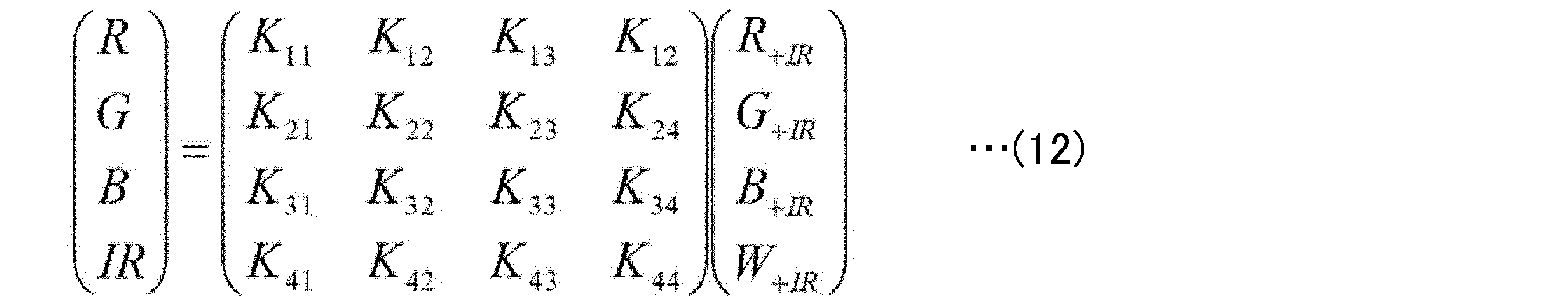
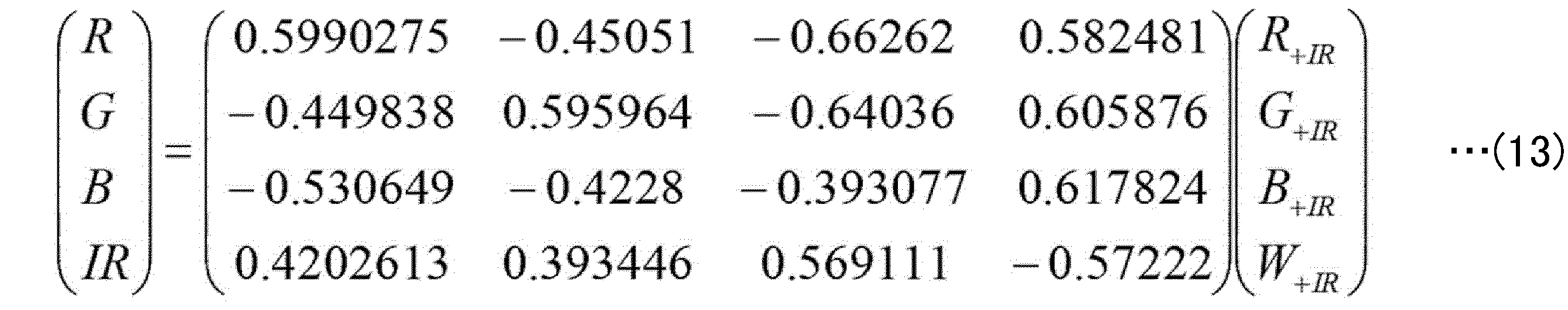
次に、本開示に係る技術を適用した撮像装置の使用例について説明する。図21は、上述した本開示に係る撮像装置1または撮像装置1’の使用例を示す図である。以下、説明のため、撮像装置1および撮像装置1’を、撮像装置1で代表させて説明を行う。
・自動停止等の安全運転や、運転者の状態の認識等のために、自動車の前方や後方、周囲、車内等を撮影する車載用センサ、走行車両や道路を監視する監視カメラ、車両間等の測距を行う測距センサ等の、交通の用に供される装置。
・ユーザのジェスチャを撮影して、そのジェスチャに従った機器操作を行うために、TVや、冷蔵庫、エアーコンディショナ等の家電に供される装置。
・内視鏡や、赤外光の受光による血管撮影を行う装置等の、医療やヘルスケアの用に供される装置。
・防犯用途の監視カメラや、人物認証用途のカメラ等の、セキュリティの用に供される装置。
・肌を撮影する肌測定器や、頭皮を撮影するマイクロスコープ等の、美容の用に供される装置。
・スポーツ用途等向けのアクションカメラやウェアラブルカメラ等の、スポーツの用に供される装置。
・畑や作物の状態を監視するためのカメラ等の、農業の用に供される装置。
本開示に係る技術(本技術)は、上述のように様々な製品へ応用することができる。例えば、本開示に係る技術は、自動車、電気自動車、ハイブリッド電気自動車、自動二輪車、自転車、パーソナルモビリティ、飛行機、ドローン、船舶、ロボット等のいずれかの種類の移動体に搭載される装置として実現されてもよい。
本開示に係る撮像装置1の応用例として、当該撮像装置1を車両に搭載して使用する場合のより具体的な例について説明する。
先ず、本開示に係る撮像装置1の第1の搭載例について説明する。図22は、本開示に係る撮像装置1を搭載可能な車両のシステム構成例を示すブロック図である。図22において、車両システム13200は、車両13000に対して設けられるCAN(Controller Area Network)に対して接続される各ユニットを含む。
次に、本開示に係る撮像装置1の第2の搭載例について説明する。図24は、本開示に係る技術が適用され得る移動体制御システムの一例である車両制御システムの概略的な構成例を示すブロック図である。
(1)
行列状の配列で配置される画素を含む画素アレイを備え、
前記画素アレイは、
それぞれ6個×6個の画素を含む複数の画素ブロックを有し、
前記画素ブロックは、
第1の波長領域の光を透過させる第1の光学フィルタが設けられた第1の画素と、
第2の波長領域の光を透過させる第2の光学フィルタが設けられた第2の画素と、
第3の波長領域の光を透過させる第3の光学フィルタが設けられた第3の画素と、
第4の波長領域の光を透過させる第4の光学フィルタが設けられた第4の画素と、
を含み、
前記配列の、行方向および列方向のそれぞれに対して前記第1の画素が1つおきに配置され、
前記配列の各行および各列は、それぞれ、前記第2の画素、前記第3の画素および前記第4の画素が1つずつ配置され、
前記画素ブロックは、さらに、
前記第2の画素、前記第3の画素および前記第4の画素を、前記配列の、該画素ブロックの対角と平行な方向である第1の斜め方向に少なくとも1つずつ含む並びと、該画素ブロックの対角と平行な方向であり該第1の斜め方向と異なる第2の斜め方向に少なくとも1つずつ含む並びと、を含む、
撮像装置。
(2)
前記画素アレイに含まれる画素のそれぞれから読み出された画素信号に対して信号処理を実行する信号処理部をさらに備え、
前記信号処理部は、
前記画素ブロックに含まれる前記第2の画素、前記第3の画素および前記第4の画素のうち、
前記配列から1つおきに選択した行および列に含まれる前記第2の画素、前記第3の画素および前記第4の画素による第1の画素群から読み出された前記画素信号と、
該第1の画素群と異なる前記第2の画素、前記第3の画素および前記第4の画素による第2の画素群から読み出された前記画素信号と、
に対してそれぞれ独立して前記信号処理を実行する、
前記(1)に記載の撮像装置。
(3)
前記信号処理部は、
前記第1の画素群に含まれる前記第2の画素、前記第3の画素および前記第4の画素から読み出された前記画素信号に基づき第1の同時化処理を実行し、
前記第2の画素群に含まれる前記第2の画素、前記第3の画素および前記第4の画素から読み出された前記画素信号に基づき、第1の同時化処理とは独立に第2の同時化処理を実行する、
前記(2)に記載の撮像装置。
(4)
前記信号処理部は、
前記第1の画素群および前記第2の画素群それぞれに含まれる前記第2の画素、前記第3の画素および前記第4の画素から読み出された前記画素信号に基づき第3の同時化処理をさらに実行し、
前記第1の同時化処理の処理結果と、前記第2の同時化処理の処理結果と、前記第3の同時化処理の処理結果と、のうち何れの処理結果を後段に出力するかを決定する、
前記(3)に記載の撮像装置。
(5)
前記信号処理部は、
前記第3の同時化処理として、前記第1の同時化処理の処理結果と、前記第2の同時化処理の処理結果と、の平均値を求める処理を実行する、
前記(4)に記載の撮像装置。
(6)
前記信号処理部は、
前記第1の同時化処理の処理結果に基づく色差と、前記第2の同時化処理の処理結果に基づく色差と、前記第3の同時化処理の処理結果に基づく色差と、のうち最も小さい色差に対応する処理結果を、後段に出力する処理結果として選択する、
前記(4)または(5)に記載の撮像装置。
(7)
前記第1の波長帯域は、可視光領域の全域に対応する波長領域であり、
前記第2の波長領域、前記第3の波長領域および前記第4の波長領域は、それぞれ赤色光領域、緑色光領域および青色光領域に対応する波長領域である、
前記(1)乃至(6)の何れかに記載の撮像装置。
(8)
前記第1の波長領域は、黄色領域に対応する波長領域であり、
前記第2の波長領域、前記第3の波長領域および前記第4の波長領域は、それぞれ赤色光領域、緑色光領域および青色光領域に対応する波長領域である、
前記(1)乃至(6)の何れかに記載の撮像装置。
(9)
前記第1の波長領域は、赤外領域に対応する波長領域であり、
前記第2の波長領域、前記第3の波長領域および前記第4の波長領域は、それぞれ赤色光領域、緑色光領域および青色光領域に対応する波長領域である、
前記(1)乃至(6)の何れかに記載の撮像装置。
(10)
前記第1の波長帯域は、可視光領域の全域に対応する波長領域であり、
前記第2の波長領域、前記第3の波長領域および前記第4の波長領域は、それぞれ赤色光領域、緑色光領域および青色光領域に対応する波長領域であり、
前記信号処理部は、
前記選択された前記処理結果と、前記第1の画素から読み出された画素信号と、に基づき、該処理結果から赤外領域に対応する成分を除去する、
前記(4)乃至(6)の何れかに記載の撮像装置。
10 撮像部
12,12’ 画像処理部
13 出力処理部
30 デュアルパスフィルタ
120,130,131,132,133 画素ブロック
300 IR分離処理部
310 赤外光成分生成部
320 可視光成分生成部
350 飽和画素検出部
1201 低周波成分同時化部
1202 高周波成分抽出部
1203,1203’ 偽色抑制処理部
1204 高周波成分復元部
Claims (10)
- 行列状の配列で配置される画素を含む画素アレイを備え、
前記画素アレイは、
それぞれ6個×6個の画素を含む複数の画素ブロックを有し、
前記画素ブロックは、
第1の波長領域の光を透過させる第1の光学フィルタが設けられた第1の画素と、
第2の波長領域の光を透過させる第2の光学フィルタが設けられた第2の画素と、
第3の波長領域の光を透過させる第3の光学フィルタが設けられた第3の画素と、
第4の波長領域の光を透過させる第4の光学フィルタが設けられた第4の画素と、
を含み、
前記配列の、行方向および列方向のそれぞれに対して前記第1の画素が1つおきに配置され、
前記配列の各行および各列は、それぞれ、前記第2の画素、前記第3の画素および前記第4の画素が1つずつ配置され、
前記画素ブロックは、さらに、
前記第2の画素、前記第3の画素および前記第4の画素を、前記配列の、該画素ブロックの対角と平行な方向である第1の斜め方向に少なくとも1つずつ含む並びと、該画素ブロックの対角と平行な方向であり該第1の斜め方向と異なる第2の斜め方向に少なくとも1つずつ含む並びと、を含む、
撮像装置。 - 前記画素アレイに含まれる画素のそれぞれから読み出された画素信号に対して信号処理を実行する信号処理部をさらに備え、
前記信号処理部は、
前記画素ブロックに含まれる前記第2の画素、前記第3の画素および前記第4の画素のうち、
前記配列から1つおきに選択した行および列に含まれる前記第2の画素、前記第3の画素および前記第4の画素による第1の画素群から読み出された前記画素信号と、
該第1の画素群と異なる前記第2の画素、前記第3の画素および前記第4の画素による第2の画素群から読み出された前記画素信号と、
に対してそれぞれ独立して前記信号処理を実行する、
請求項1に記載の撮像装置。 - 前記信号処理部は、
前記第1の画素群に含まれる前記第2の画素、前記第3の画素および前記第4の画素から読み出された前記画素信号に基づき第1の同時化処理を実行し、
前記第2の画素群に含まれる前記第2の画素、前記第3の画素および前記第4の画素から読み出された前記画素信号に基づき、第1の同時化処理とは独立に第2の同時化処理を実行する、
請求項2に記載の撮像装置。 - 前記信号処理部は、
前記第1の画素群および前記第2の画素群それぞれに含まれる前記第2の画素、前記第3の画素および前記第4の画素から読み出された前記画素信号に基づき第3の同時化処理をさらに実行し、
前記第1の同時化処理の処理結果と、前記第2の同時化処理の処理結果と、前記第3の同時化処理の処理結果と、のうち何れの処理結果を後段に出力するかを決定する、
請求項3に記載の撮像装置。 - 前記信号処理部は、
前記第3の同時化処理として、前記第1の同時化処理の処理結果と、前記第2の同時化処理の処理結果と、の平均値を求める処理を実行する、
請求項4に記載の撮像装置。 - 前記信号処理部は、
前記第1の同時化処理の処理結果に基づく色差と、前記第2の同時化処理の処理結果に基づく色差と、前記第3の同時化処理の処理結果に基づく色差と、のうち最も小さい色差に対応する処理結果を、後段に出力する処理結果として選択する、
請求項4に記載の撮像装置。 - 前記第1の波長領域は、可視光領域の全域に対応する波長領域であり、
前記第2の波長領域、前記第3の波長領域および前記第4の波長領域は、それぞれ赤色光領域、緑色光領域および青色光領域に対応する波長領域である、
請求項1に記載の撮像装置。 - 前記第1の波長領域は、黄色領域に対応する波長領域であり、
前記第2の波長領域、前記第3の波長領域および前記第4の波長領域は、それぞれ赤色光領域、緑色光領域および青色光領域に対応する波長領域である、
請求項1に記載の撮像装置。 - 前記第1の波長領域は、赤外領域に対応する波長領域であり、
前記第2の波長領域、前記第3の波長領域および前記第4の波長領域は、それぞれ赤色光領域、緑色光領域および青色光領域に対応する波長領域である、
請求項1に記載の撮像装置。 - 前記第1の波長領域は、可視光領域の全域に対応する波長領域であり、
前記第2の波長領域、前記第3の波長領域および前記第4の波長領域は、それぞれ赤色光領域、緑色光領域および青色光領域に対応する波長領域であり、
前記信号処理部は、
前記選択された前記処理結果と、前記第1の画素から読み出された画素信号と、に基づき、該処理結果から赤外領域に対応する成分を除去する、
請求項4に記載の撮像装置。
Priority Applications (5)
| Application Number | Priority Date | Filing Date | Title |
|---|---|---|---|
| EP20868258.3A EP4036617A4 (en) | 2019-09-26 | 2020-09-16 | IMAGING DEVICE |
| JP2021548850A JP7566761B2 (ja) | 2019-09-26 | 2020-09-16 | 撮像装置 |
| CN202080057082.7A CN114270798B (zh) | 2019-09-26 | 2020-09-16 | 摄像装置 |
| KR1020227008830A KR20220068996A (ko) | 2019-09-26 | 2020-09-16 | 촬상 장치 |
| US17/761,425 US20220368867A1 (en) | 2019-09-26 | 2020-09-16 | Imaging device |
Applications Claiming Priority (2)
| Application Number | Priority Date | Filing Date | Title |
|---|---|---|---|
| JP2019-175596 | 2019-09-26 | ||
| JP2019175596 | 2019-09-26 |
Publications (1)
| Publication Number | Publication Date |
|---|---|
| WO2021060118A1 true WO2021060118A1 (ja) | 2021-04-01 |
Family
ID=75166965
Family Applications (1)
| Application Number | Title | Priority Date | Filing Date |
|---|---|---|---|
| PCT/JP2020/035144 Ceased WO2021060118A1 (ja) | 2019-09-26 | 2020-09-16 | 撮像装置 |
Country Status (7)
| Country | Link |
|---|---|
| US (1) | US20220368867A1 (ja) |
| EP (1) | EP4036617A4 (ja) |
| JP (1) | JP7566761B2 (ja) |
| KR (1) | KR20220068996A (ja) |
| CN (1) | CN114270798B (ja) |
| TW (1) | TWI842952B (ja) |
| WO (1) | WO2021060118A1 (ja) |
Cited By (1)
| Publication number | Priority date | Publication date | Assignee | Title |
|---|---|---|---|---|
| WO2023012989A1 (ja) * | 2021-08-05 | 2023-02-09 | ソニーセミコンダクタソリューションズ株式会社 | 撮像装置 |
Families Citing this family (3)
| Publication number | Priority date | Publication date | Assignee | Title |
|---|---|---|---|---|
| KR102883962B1 (ko) * | 2020-12-21 | 2025-11-10 | 에스케이하이닉스 주식회사 | 이미지 센싱 장치 |
| US11792535B2 (en) * | 2021-08-10 | 2023-10-17 | Samsung Electronics Co., Ltd. | System and method to improve quality in under-display camera system with radially increasing distortion |
| US12244937B2 (en) * | 2022-07-29 | 2025-03-04 | Texas Instruments Incorporated | RGB-IR pixel pattern conversion via conversion engine |
Citations (4)
| Publication number | Priority date | Publication date | Assignee | Title |
|---|---|---|---|---|
| JPH0230751B2 (ja) | 1983-08-06 | 1990-07-09 | Kikusui Kagaku Kogyo Kk | |
| WO2013145487A1 (ja) | 2012-03-27 | 2013-10-03 | ソニー株式会社 | 画像処理装置、撮像素子、および画像処理方法、並びにプログラム |
| JP2016025626A (ja) * | 2014-07-24 | 2016-02-08 | ソニー株式会社 | 撮像素子、撮像方法、撮像装置 |
| JP2016511562A (ja) * | 2013-01-22 | 2016-04-14 | サムスン エレクトロニクス カンパニー リミテッド | 複数のマイクロレンズを使用して撮影する撮影装置及びその撮影方法 |
Family Cites Families (20)
| Publication number | Priority date | Publication date | Assignee | Title |
|---|---|---|---|---|
| JPH0230751Y2 (ja) | 1981-01-13 | 1990-08-20 | ||
| US7508431B2 (en) * | 2004-06-17 | 2009-03-24 | Hoya Corporation | Solid state imaging device |
| JP5151075B2 (ja) * | 2005-06-21 | 2013-02-27 | ソニー株式会社 | 画像処理装置及び画像処理方法、撮像装置、並びにコンピュータ・プログラム |
| JP5106870B2 (ja) * | 2006-06-14 | 2012-12-26 | 株式会社東芝 | 固体撮像素子 |
| US7769229B2 (en) * | 2006-11-30 | 2010-08-03 | Eastman Kodak Company | Processing images having color and panchromatic pixels |
| JP5085140B2 (ja) * | 2007-01-05 | 2012-11-28 | 株式会社東芝 | 固体撮像装置 |
| JP4500360B2 (ja) * | 2007-06-15 | 2010-07-14 | パナソニック株式会社 | 画像処理装置 |
| JP2009232351A (ja) * | 2008-03-25 | 2009-10-08 | Seiko Epson Corp | 撮像装置及びカラーフィルタアレイ |
| JP5442571B2 (ja) * | 2010-09-27 | 2014-03-12 | パナソニック株式会社 | 固体撮像装置及び撮像装置 |
| JP5581954B2 (ja) * | 2010-10-07 | 2014-09-03 | ソニー株式会社 | 固体撮像装置、固体撮像装置の製造方法、及び電子機器 |
| EP2685711B1 (en) * | 2011-03-09 | 2017-08-30 | Fujifilm Corporation | Color image pickup device |
| JP2013145487A (ja) | 2012-01-16 | 2013-07-25 | Seiko Epson Corp | データ転送装置およびデータ処理システム |
| JP5500193B2 (ja) * | 2012-03-21 | 2014-05-21 | ソニー株式会社 | 固体撮像装置、撮像装置、撮像及び信号処理方法 |
| JP5698873B2 (ja) * | 2012-07-06 | 2015-04-08 | 富士フイルム株式会社 | カラー撮像素子および撮像装置 |
| JP5927068B2 (ja) * | 2012-07-06 | 2016-05-25 | 富士フイルム株式会社 | カラー撮像素子 |
| JP2015109588A (ja) * | 2013-12-05 | 2015-06-11 | 株式会社東芝 | 信号処理装置及び撮像システム |
| JP6473350B2 (ja) * | 2015-03-05 | 2019-02-20 | 独立行政法人国立高等専門学校機構 | カラー撮像素子 |
| JP6598507B2 (ja) * | 2015-05-11 | 2019-10-30 | キヤノン株式会社 | 撮像装置、撮像システム、信号処理方法 |
| US10015416B2 (en) * | 2016-05-24 | 2018-07-03 | Semiconductor Components Industries, Llc | Imaging systems with high dynamic range and phase detection pixels |
| JP6843682B2 (ja) * | 2017-04-07 | 2021-03-17 | キヤノン株式会社 | 撮像素子および撮像装置 |
-
2020
- 2020-09-16 KR KR1020227008830A patent/KR20220068996A/ko active Pending
- 2020-09-16 WO PCT/JP2020/035144 patent/WO2021060118A1/ja not_active Ceased
- 2020-09-16 US US17/761,425 patent/US20220368867A1/en not_active Abandoned
- 2020-09-16 EP EP20868258.3A patent/EP4036617A4/en not_active Withdrawn
- 2020-09-16 JP JP2021548850A patent/JP7566761B2/ja active Active
- 2020-09-16 CN CN202080057082.7A patent/CN114270798B/zh active Active
- 2020-09-18 TW TW109132438A patent/TWI842952B/zh not_active IP Right Cessation
Patent Citations (4)
| Publication number | Priority date | Publication date | Assignee | Title |
|---|---|---|---|---|
| JPH0230751B2 (ja) | 1983-08-06 | 1990-07-09 | Kikusui Kagaku Kogyo Kk | |
| WO2013145487A1 (ja) | 2012-03-27 | 2013-10-03 | ソニー株式会社 | 画像処理装置、撮像素子、および画像処理方法、並びにプログラム |
| JP2016511562A (ja) * | 2013-01-22 | 2016-04-14 | サムスン エレクトロニクス カンパニー リミテッド | 複数のマイクロレンズを使用して撮影する撮影装置及びその撮影方法 |
| JP2016025626A (ja) * | 2014-07-24 | 2016-02-08 | ソニー株式会社 | 撮像素子、撮像方法、撮像装置 |
Cited By (1)
| Publication number | Priority date | Publication date | Assignee | Title |
|---|---|---|---|---|
| WO2023012989A1 (ja) * | 2021-08-05 | 2023-02-09 | ソニーセミコンダクタソリューションズ株式会社 | 撮像装置 |
Also Published As
| Publication number | Publication date |
|---|---|
| TW202129313A (zh) | 2021-08-01 |
| TWI842952B (zh) | 2024-05-21 |
| JPWO2021060118A1 (ja) | 2021-04-01 |
| US20220368867A1 (en) | 2022-11-17 |
| KR20220068996A (ko) | 2022-05-26 |
| EP4036617A4 (en) | 2022-11-16 |
| CN114270798A (zh) | 2022-04-01 |
| JP7566761B2 (ja) | 2024-10-15 |
| CN114270798B (zh) | 2023-10-24 |
| EP4036617A1 (en) | 2022-08-03 |
Similar Documents
| Publication | Publication Date | Title |
|---|---|---|
| JP7105754B2 (ja) | 撮像装置、及び、撮像装置の制御方法 | |
| JP7600129B2 (ja) | 撮像装置 | |
| JP7566761B2 (ja) | 撮像装置 | |
| US11394913B2 (en) | Solid-state imaging element, electronic device, and method for controlling correction of luminance in the solid-state imaging element | |
| TWI800722B (zh) | 圖像辨識裝置及圖像辨識方法 | |
| WO2018190126A1 (ja) | 固体撮像装置、及び電子機器 | |
| CN113875217B (zh) | 图像识别装置和图像识别方法 | |
| US11605661B2 (en) | Image processing apparatus, image processing method, and solid-state imaging apparatus to detect polarization properties of each color | |
| WO2020230660A1 (ja) | 画像認識装置、固体撮像装置、および画像認識方法 | |
| JP6803989B2 (ja) | 固体撮像装置及びその駆動方法 | |
| WO2019003951A1 (ja) | 固体撮像装置、及び電子機器 | |
| JP7144926B2 (ja) | 撮像制御装置、撮像装置、および、撮像制御装置の制御方法 | |
| WO2017175492A1 (ja) | 画像処理装置、画像処理方法、コンピュータプログラム及び電子機器 | |
| WO2018207666A1 (ja) | 撮像素子及びその駆動方法、並びに、電子機器 | |
| WO2017169274A1 (ja) | 撮像制御装置、撮像制御方法、コンピュータプログラム及び電子機器 | |
| WO2018139187A1 (ja) | 固体撮像装置およびその駆動方法、並びに電子機器 | |
| US20200402206A1 (en) | Image processing device, image processing method, and program | |
| WO2022019025A1 (ja) | 情報処理装置、情報処理システム、情報処理方法、及び情報処理プログラム | |
| US20240078803A1 (en) | Information processing apparatus, information processing method, computer program, and sensor apparatus | |
| WO2020230635A1 (ja) | 撮像装置および撮像方法 | |
| WO2022219874A1 (ja) | 信号処理装置および方法、並びにプログラム | |
| WO2018211985A1 (ja) | 撮像素子、および撮像素子の制御方法、撮像装置、並びに電子機器 | |
| JP2020017552A (ja) | 固体撮像素子、撮像装置、および、固体撮像素子の制御方法 |
Legal Events
| Date | Code | Title | Description |
|---|---|---|---|
| 121 | Ep: the epo has been informed by wipo that ep was designated in this application |
Ref document number: 20868258 Country of ref document: EP Kind code of ref document: A1 |
|
| ENP | Entry into the national phase |
Ref document number: 2021548850 Country of ref document: JP Kind code of ref document: A |
|
| NENP | Non-entry into the national phase |
Ref country code: DE |
|
| ENP | Entry into the national phase |
Ref document number: 2020868258 Country of ref document: EP Effective date: 20220426 |
|
| WWW | Wipo information: withdrawn in national office |
Ref document number: 2020868258 Country of ref document: EP |