WO2021131908A1 - Circuit audio et procédé de reproduction de signal dsd - Google Patents
Circuit audio et procédé de reproduction de signal dsd Download PDFInfo
- Publication number
- WO2021131908A1 WO2021131908A1 PCT/JP2020/046771 JP2020046771W WO2021131908A1 WO 2021131908 A1 WO2021131908 A1 WO 2021131908A1 JP 2020046771 W JP2020046771 W JP 2020046771W WO 2021131908 A1 WO2021131908 A1 WO 2021131908A1
- Authority
- WO
- WIPO (PCT)
- Prior art keywords
- dsd
- shift register
- circuit
- bit
- volume
- Prior art date
- Legal status (The legal status is an assumption and is not a legal conclusion. Google has not performed a legal analysis and makes no representation as to the accuracy of the status listed.)
- Ceased
Links
Images




Classifications
-
- H—ELECTRICITY
- H04—ELECTRIC COMMUNICATION TECHNIQUE
- H04R—LOUDSPEAKERS, MICROPHONES, GRAMOPHONE PICK-UPS OR LIKE ACOUSTIC ELECTROMECHANICAL TRANSDUCERS; ELECTRIC HEARING AIDS; PUBLIC ADDRESS SYSTEMS
- H04R3/00—Circuits for transducers
- H04R3/04—Circuits for transducers for correcting frequency response
-
- G—PHYSICS
- G06—COMPUTING OR CALCULATING; COUNTING
- G06F—ELECTRIC DIGITAL DATA PROCESSING
- G06F1/00—Details not covered by groups G06F3/00 - G06F13/00 and G06F21/00
- G06F1/04—Generating or distributing clock signals or signals derived directly therefrom
- G06F1/08—Clock generators with changeable or programmable clock frequency
-
- G—PHYSICS
- G06—COMPUTING OR CALCULATING; COUNTING
- G06F—ELECTRIC DIGITAL DATA PROCESSING
- G06F3/00—Input arrangements for transferring data to be processed into a form capable of being handled by the computer; Output arrangements for transferring data from processing unit to output unit, e.g. interface arrangements
- G06F3/16—Sound input; Sound output
- G06F3/165—Management of the audio stream, e.g. setting of volume, audio stream path
-
- G—PHYSICS
- G10—MUSICAL INSTRUMENTS; ACOUSTICS
- G10K—SOUND-PRODUCING DEVICES; METHODS OR DEVICES FOR PROTECTING AGAINST, OR FOR DAMPING, NOISE OR OTHER ACOUSTIC WAVES IN GENERAL; ACOUSTICS NOT OTHERWISE PROVIDED FOR
- G10K15/00—Acoustics not otherwise provided for
- G10K15/02—Synthesis of acoustic waves
-
- H—ELECTRICITY
- H03—ELECTRONIC CIRCUITRY
- H03G—CONTROL OF AMPLIFICATION
- H03G3/00—Gain control in amplifiers or frequency changers
- H03G3/02—Manually-operated control
-
- G—PHYSICS
- G10—MUSICAL INSTRUMENTS; ACOUSTICS
- G10L—SPEECH ANALYSIS TECHNIQUES OR SPEECH SYNTHESIS; SPEECH RECOGNITION; SPEECH OR VOICE PROCESSING TECHNIQUES; SPEECH OR AUDIO CODING OR DECODING
- G10L19/00—Speech or audio signals analysis-synthesis techniques for redundancy reduction, e.g. in vocoders; Coding or decoding of speech or audio signals, using source filter models or psychoacoustic analysis
-
- H—ELECTRICITY
- H03—ELECTRONIC CIRCUITRY
- H03M—CODING; DECODING; CODE CONVERSION IN GENERAL
- H03M1/00—Analogue/digital conversion; Digital/analogue conversion
- H03M1/66—Digital/analogue converters
- H03M1/68—Digital/analogue converters with conversions of different sensitivity, i.e. one conversion relating to the more significant digital bits and another conversion to the less significant bits
- H03M1/687—Segmented, i.e. the more significant bit converter being of the unary decoded type and the less significant bit converter being of the binary weighted type
-
- H—ELECTRICITY
- H03—ELECTRONIC CIRCUITRY
- H03M—CODING; DECODING; CODE CONVERSION IN GENERAL
- H03M1/00—Analogue/digital conversion; Digital/analogue conversion
- H03M1/66—Digital/analogue converters
- H03M1/74—Simultaneous conversion
- H03M1/742—Simultaneous conversion using current sources as quantisation value generators
-
- H—ELECTRICITY
- H04—ELECTRIC COMMUNICATION TECHNIQUE
- H04R—LOUDSPEAKERS, MICROPHONES, GRAMOPHONE PICK-UPS OR LIKE ACOUSTIC ELECTROMECHANICAL TRANSDUCERS; ELECTRIC HEARING AIDS; PUBLIC ADDRESS SYSTEMS
- H04R2430/00—Signal processing covered by H04R, not provided for in its groups
- H04R2430/01—Aspects of volume control, not necessarily automatic, in sound systems
Definitions
- the present disclosure relates to audio signal processing, and particularly to DSD signal reproduction technology.
- DSD Direct Stream Digital
- SACD Super Audio CD
- the DSD method is a type of PDM (Pulse Density Modulation) in which an audio waveform is recorded as a 1-bit pulse density modulated bitstream, and in principle, it is passed through a low-pass filter. The original audio waveform can be reproduced.
- PDM Pulse Density Modulation
- the DSD format audio signal playback method can be divided into two types: non-native playback and native playback.
- non-native playback the DSD signal is once converted into a PCM (Pulse Code Modulation) signal, and then converted into an analog audio signal by a D / A converter.
- PCM Pulse Code Modulation
- the DSD signal is not converted into a PCM signal, but D / A conversion is performed as it is and converted into an analog audio signal.
- various digital signal processing such as volume control and equalizing processing can be applied to the PCM signal by DSP (Digital Signal Processor or Digital Sound Processor).
- DSP Digital Signal Processor or Digital Sound Processor
- the PCM conversion causes a delay and is easily affected by jitter, so that the native reproduction is superior in terms of sound quality.
- This disclosure was made in such a situation, and one of the exemplary purposes of that aspect is to provide an audio circuit that is DSD native and volume controllable.
- the audio circuit includes a volume circuit that processes a DSD signal including DSD (Direct Stream Digital) data and a DSD clock.
- the volume circuit has an N-bit (N ⁇ 2) first shift register for holding DSD data and an N-bit (N-M) bit (0) corresponding to a gain setting value among the N bits stored in the first shift register.
- N-M N-bit
- ⁇ M ⁇ N includes a replacement circuit that replaces the mute bit string having a mark ratio of substantially 50%.
- volume control is possible with DSD native.
- the audio circuit includes a volume circuit.
- the volume circuit corresponds to the gain setting value of the first shift register of N bits (N ⁇ 2) holding the DSD data of the DSD (Direct Stream Digital) signal and the N bits stored in the first shift register. It includes a replacement circuit that replaces the (NM) bits (0 ⁇ M ⁇ N) with a mute bit string having a mark ratio of substantially 50%.
- the mark ratio approaches 50% and the mute state approaches as the gain setting value becomes smaller. Therefore, volume control in DSD native is possible.
- the mute bit string may be inverted for each DSD clock cycle. As a result, the time average of the mark rate of the mute bit string approaches 50%, so that deterioration of sound quality can be suppressed.
- a pseudo-random bit sequence having a mark rate of 50% may be used as the mute bit string.
- PRBS pseudo-random bit sequence
- the substitution circuit is an N-bit second shift register that inputs data that is inverted every cycle of the DSD clock, an M bit from one end of the first shift register, and an M bit from the other end of the second shift register. It may include a coupler that couples (NM) bits.
- the second shift register can generate a mute bit string that is inverted every cycle of the DSD clock.
- the volume circuit may further include a counter that changes the gain set value from the initial value before the volume change toward the target value after the volume change when the volume set value is changed.
- the time or slope from the initial value to the target value of the gain set value may be set.
- the audio circuit may further include a current segment D / A converter that receives the N bits generated by the replacement circuit as input.
- the "state in which the member A is connected to the member B" means that the member A and the member B are physically directly connected, or the member A and the member B are electrically connected to each other. It also includes the case of being indirectly connected via other members, which does not substantially affect the connection state or does not impair the functions and effects performed by the combination thereof.
- a state in which the member C is provided between the member A and the member B means that the member A and the member C, or the member B and the member C are directly connected, and their electricity. It also includes the case of being indirectly connected via other members, which does not substantially affect the connection state, or does not impair the functions and effects produced by the combination thereof.
- FIG. 1 is a circuit diagram of an audio circuit 100 according to an embodiment.
- the audio circuit 100 is an IC (Integrated Circuit) integrated on one semiconductor substrate.
- the audio circuit 100 is a DAC chip in which a D / A converter 102 and a volume circuit 110 are integrated.
- the audio circuit 100 has data pin DATA and clock pin CLK, and receives a DSD signal including DSD data D1 and DSD clock CLK.
- the volume circuit 110 receives the DSD signal including the DSD data D1 and the DSD clock CLK, and performs volume control according to the volume set value VOL.
- the appearance probability of 0 and 1 is 50% in the mute state, and the deviation from 50% becomes the audio signal component.
- the volume circuit 110 includes a first shift register 112 and a replacement circuit 114.
- the substitution circuit 114 has a mark ratio of substantially 50 for (NM) bits (0 ⁇ M ⁇ N) corresponding to the gain setting value in the N-bit bit string D2 stored in the first shift register 112. It is replaced with the mute bit string MB which is%, and the replaced bit string D3 is output.
- the number of bits M is N at the maximum gain and 0 at the minimum gain.
- FIG. 2 is an operation waveform diagram of the audio circuit 100 of FIG.
- D1 indicates DSD data.
- the DSD data is a pulse density modulated 1 and 0 bitstream.
- N bits of data D2 of the DSD data D1 are stored in the first shift register 112.
- the replacement circuit 114 replaces the (NM) bit of the N-bit data D2 with a mute bit string MB having a mark rate of 50%.
- the original bit is stored in the M bit.
- the mute bit string MB is a bit string in which 1s and 0s are alternately arranged.
- the replaced data D3 is input to the A / D converter in the subsequent stage and converted into an analog signal.
- the audio circuit 100 repeats the same process while shifting the bit string D2 stored in the first shift register 112 from the DSD data D1 to the right for each clock cycle.
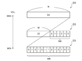
- FIG. 3 is a diagram illustrating volume control in the audio circuit 100 of FIG.
- VOL is the maximum value MAX
- M N
- DSD data D2 that is, D1
- the DSD data to be reproduced is in a mute state because the mark rate is 50%.
- the volume set value VOL takes an intermediate value between the minimum value MIN and the maximum value MAX, 0 ⁇ M ⁇ N, and a part of the input DSD data D2 is replaced with the mute bit string MB.
- the effective volume of the DSD data to be reproduced is M / N times higher than that when the volume setting value is the maximum.
- volume control in DSD native is possible. Since the volume control by DSD native does not require PCM conversion, the delay time at the time of audio reproduction can be reduced, and the power consumption of the circuit can be reduced. Further, since the volume circuit 110 can be configured by a combination of a shift register and a bit replacement circuit, it is simple and the circuit area can be small.
- the present disclosure covers various devices and methods that are grasped as the block diagram or circuit diagram of FIG. 1 or derived from the above description, and are not limited to a specific configuration.
- more specific configuration examples and examples will be described not to narrow the scope of the present disclosure but to help understanding the essence and operation of the disclosure and to clarify them.
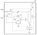
- FIG. 4 is a circuit diagram of the volume circuit 110 according to the embodiment.
- the mute bit string MB is inverted every cycle of the DSD clock CLK.
- the substitution circuit 114 includes a second shift register 116 and a coupler 118.
- the second shift register 116 has N bits like the first shift register 112, and receives data (referred to as clock inversion data) D4 that is inverted every cycle of the DSD clock CLK at its input.
- the bit string stored in the second shift register 116 is inverted every cycle of the DSD clock CLK.
- the clock inversion data D4 can be composed of a flip-flop 115 and an inverter 117.
- the coupler 118 combines M bits from one end of the first shift register 112 and (NM) bits from the other end of the second shift register 116, and outputs N-bit DSD data D3.
- the replacement circuit 114 further includes a counter 120.
- the counter 120 changes the gain set value, that is, M, from the initial value before the volume change toward the target value after the volume change.
- the time or slope from the initial value to the target value of the gain set value M can be set by using a register.
- FIG. 5 is a circuit diagram of the volume circuit 110 according to the modified example.
- the clock inversion data D4 is generated by inverting the output of the second shift register 116 by the inverter 116.
- the DSD clock may be delayed by about 1/4 cycle, and the signal may be used as the clock inversion data D4.
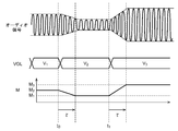
- FIG. 6 is an operation waveform diagram of the volume circuit 110 of FIG. 4 or FIG.
- the volume set value VOL is a certain value V 1 before the time t 0
- the gain set value M is a value M 1 corresponding to the volume set value V 1 .
- the user changes the volume set value VOL to the value V 2 .
- the counter 120 changes the gain setting value M from the initial value M 1 corresponding to the volume setting value V 1 before the change to the target value M 2 corresponding to the volume setting value V 2 after the change. Decrease over transition time ⁇ .
- the amplitude of the audio signal that is, the volume, which is the output of the D / A converter, gradually decreases.
- the user changes the volume setting value VOL to the value V 3.
- the counter 120 moves the gain setting value M from the initial value M 2 corresponding to the volume setting value V 2 before the change to the target value M 3 corresponding to the volume setting value V 3 after the change. And increase over the transition time ⁇ .
- the amplitude of the audio signal that is, the volume, which is the output of the D / A converter, gradually increases.
- the counter 120 operates so that the transition time ⁇ of the gain set value M becomes constant, but the present invention is not limited to this, and the counter 120 may operate so that the slope of the gain set value M becomes constant.
- the transition time ⁇ is on the order of tens of milliseconds to hundreds of milliseconds.
- FIG. 7 is a diagram illustrating the internal operation of the volume circuit 110 of FIG.
- the gain setting value M is fixed at a certain value of 0 ⁇ M ⁇ N.
- 1 and 0 of the mute bit string MB included in the DSD data D3 after volume control are inverted in the cycle of the DSD clock CLK.
- the audio component D2 included in the DSD data D3 is shifted by 1 bit for each cycle of the DSD clock CLK.
- the above is the internal operation of the volume circuit 110.
- a fixed pattern is used as the mute bit MB
- the mark rate of the mute bit string MB deviates from 50%, a DC offset occurs, which causes deterioration of sound quality.
- the volume circuit 110 of FIG. 6 even when the NM is an odd number, the time average value of the mark rate of the mute bit string MB is 50%, so that the influence of the DC offset can be suppressed.
- a pseudo-random signal PRBS having a mark rate of 50% may be used as the mute bit string.
- the second shift register 116 in FIG. 4 may be replaced with an N-bit PRBS generator. Even when PRBS is used, the time average value of the mark rate of the mute bit string MB can be approached to 50%.
- Modification 2 A fixed pattern may be used as the mute bit string. In this case, a DC offset is generated, but the circuit configuration can be further simplified.
- the gain setting value M may be changed so that (MN) becomes an even number. In this case, the DC offset does not occur.
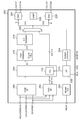
- FIG. 8 is a block diagram of the D / A converter IC200.
- the D / A converter IC 200 is configured using the architecture of the audio circuit 100 described above.
- the D / A converter IC200 receives an audio signal in PCM format or DSD format, converts it into an analog audio signal, and outputs it.
- DSD platform a DSD sound source is connected to the DSDCLK pin, DSD1 pin, and DSD2 pin of the D / A converter IC200, and a 2-channel audio signal is input in the DSD format.
- the BCLK pin and the DSDCLK pin, the LRCLK pin and the DSDCL2 pin, and the DIN pin and the DSDCL1 pin are shared.
- the PCM interface 210, audio function controller 214, oversampling digital filter 216, and delta-sigma modulator 218 become active on the PCM platform.
- the audio function controller 214 performs signal processing such as volume control on the PCM signal received by the PCM interface 210.
- the oversampling digital filter 216 oversamples the output of the audio function controller 214, and controls the frequency characteristics by the digital filter.
- the delta-sigma modulator 218 ⁇ -modulates the output of the oversampling digital filter 216.
- the output of the delta-sigma modulator 218 is two channels, and each channel is an N-bit PDM signal.
- the N-bit ⁇ 2 channel PDM signal is input to the current segments DAC 224 and 226 for each channel via the selector 220.
- the current segments DAC 224 and 226 correspond to the D / A converter 102 of FIG.
- the reference voltage source 228 supplies a reference voltage to the current segments DAC 224 and 226.
- the current segments DAC 224 and 226 have a differential current output, but are not limited to this, and may be a single-ended output or a voltage output.
- the DSD interface 212 becomes active on the DSD platform and receives a DSD signal, specifically a DSD clock and two channels of DSD data, from an external DSD sound source.
- the first shift register 112 of the volume circuit 110 may be configured as part of the DSD interface 212.
- the audio function controller 214 includes the above-mentioned volume circuit 110.
- the volume circuit 110 performs volume control on the two-channel DSD signal received by the DSD interface 212.
- the volume-controlled DSD signal (DSD data D3 described above) output from the volume circuit 110 is input to the current segments DAC224 and 226 for each channel via the selector 220.
- the clock generator 230 multiplies the reference clock to generate a master clock.
- Serial interface 232 is I 2 C or SPI interface and the data pin SDA and the clock pin SCK is an external host processor is connected.
- the serial interface 232 receives the volume setting value and various parameters from the host processor. This parameter includes the time constant and slope when the volume is soft-transitioned.
- the volume setting value received by the serial interface 232 is supplied to the audio function controller 214.
- the system controller 234 controls the entire D / A converter IC200 in an integrated manner.
- a reset signal is input to the system controller 234.
- This disclosure can be used for audio signal processing.
- Audio circuit 102 D / A converter 110 Volume circuit 112 1st shift register 114 Substitution circuit 116 2nd shift register 118 Coupler 120 Counter 200 D / A converter IC 210 PCM Interface 212 DSD Interface 214 Audio Function Controller 216 Oversampling Digital Filter 218 ⁇ Modulator 220 Selector 224,226 Current Segment DAC 228 Reference voltage source 230 Clock generator 232 Serial interface 234 System controller
Landscapes
- Engineering & Computer Science (AREA)
- Theoretical Computer Science (AREA)
- Physics & Mathematics (AREA)
- Acoustics & Sound (AREA)
- General Physics & Mathematics (AREA)
- General Engineering & Computer Science (AREA)
- Signal Processing (AREA)
- Health & Medical Sciences (AREA)
- Audiology, Speech & Language Pathology (AREA)
- General Health & Medical Sciences (AREA)
- Multimedia (AREA)
- Human Computer Interaction (AREA)
- Control Of Amplification And Gain Control (AREA)
Abstract
Circuit audio 100 comprenant un circuit de volume 110 qui traite un signal DSD comportant des données DSD et une horloge DSD. Le circuit de volume 110 comprend un premier registre à décalage 112 et un circuit de remplacement 114. Le premier registre à décalage 112 conserve N bits des données DSD. Le circuit de remplacement 114 remplace (N - M) bits (0 ≤ M ≤ N), correspondant à une valeur de réglage de gain parmi les N bits stockés dans le premier registre à décalage 112, par une chaîne de bits pour une désactivation présentant un taux de marque de sensiblement 50 %.
Priority Applications (3)
| Application Number | Priority Date | Filing Date | Title |
|---|---|---|---|
| JP2021567306A JP7736568B2 (ja) | 2019-12-27 | 2020-12-15 | オーディオ回路、dsd信号の再生方法 |
| CN202080084037.0A CN114766051A (zh) | 2019-12-27 | 2020-12-15 | 音频电路、dsd信号的再现方法 |
| US17/850,126 US12167213B2 (en) | 2019-12-27 | 2022-06-27 | Audio circuit, and reproduction method of DSD signal |
Applications Claiming Priority (2)
| Application Number | Priority Date | Filing Date | Title |
|---|---|---|---|
| JP2019239618 | 2019-12-27 | ||
| JP2019-239618 | 2019-12-27 |
Related Child Applications (1)
| Application Number | Title | Priority Date | Filing Date |
|---|---|---|---|
| US17/850,126 Continuation US12167213B2 (en) | 2019-12-27 | 2022-06-27 | Audio circuit, and reproduction method of DSD signal |
Publications (1)
| Publication Number | Publication Date |
|---|---|
| WO2021131908A1 true WO2021131908A1 (fr) | 2021-07-01 |
Family
ID=76574764
Family Applications (1)
| Application Number | Title | Priority Date | Filing Date |
|---|---|---|---|
| PCT/JP2020/046771 Ceased WO2021131908A1 (fr) | 2019-12-27 | 2020-12-15 | Circuit audio et procédé de reproduction de signal dsd |
Country Status (4)
| Country | Link |
|---|---|
| US (1) | US12167213B2 (fr) |
| JP (1) | JP7736568B2 (fr) |
| CN (1) | CN114766051A (fr) |
| WO (1) | WO2021131908A1 (fr) |
Families Citing this family (1)
| Publication number | Priority date | Publication date | Assignee | Title |
|---|---|---|---|---|
| CN116913294B (zh) * | 2023-09-11 | 2023-12-19 | 归芯科技(深圳)有限公司 | Pcm信号的处理方法、装置、数字音频系统及电子设备 |
Citations (1)
| Publication number | Priority date | Publication date | Assignee | Title |
|---|---|---|---|---|
| US20170372717A1 (en) * | 2016-06-24 | 2017-12-28 | Cirrus Logic International Semiconductor Ltd. | Digital volume control |
Family Cites Families (5)
| Publication number | Priority date | Publication date | Assignee | Title |
|---|---|---|---|---|
| JPH09153748A (ja) * | 1995-11-30 | 1997-06-10 | Sharp Corp | 音量可変装置 |
| JP2008249973A (ja) * | 2007-03-30 | 2008-10-16 | Sony Corp | ボリューム制御装置、ボリューム制御方法及びそのプログラム |
| WO2015176244A1 (fr) * | 2014-05-21 | 2015-11-26 | Qualcomm Incorporated | Convertisseur parallèle-série et série-parallèle pour bus de données parallèles à rapport impair |
| US10424311B2 (en) * | 2017-01-30 | 2019-09-24 | Cirrus Logic, Inc. | Auto-mute audio processing |
| EP3471271A1 (fr) * | 2017-10-16 | 2019-04-17 | Acoustical Beauty | Convolutions améliorées de signaux numériques utilisant une optimisation des exigences de bits d'un signal numérique cible |
-
2020
- 2020-12-15 CN CN202080084037.0A patent/CN114766051A/zh active Pending
- 2020-12-15 WO PCT/JP2020/046771 patent/WO2021131908A1/fr not_active Ceased
- 2020-12-15 JP JP2021567306A patent/JP7736568B2/ja active Active
-
2022
- 2022-06-27 US US17/850,126 patent/US12167213B2/en active Active
Patent Citations (1)
| Publication number | Priority date | Publication date | Assignee | Title |
|---|---|---|---|---|
| US20170372717A1 (en) * | 2016-06-24 | 2017-12-28 | Cirrus Logic International Semiconductor Ltd. | Digital volume control |
Also Published As
| Publication number | Publication date |
|---|---|
| CN114766051A (zh) | 2022-07-19 |
| US20220329942A1 (en) | 2022-10-13 |
| JPWO2021131908A1 (fr) | 2021-07-01 |
| US12167213B2 (en) | 2024-12-10 |
| JP7736568B2 (ja) | 2025-09-09 |
Similar Documents
| Publication | Publication Date | Title |
|---|---|---|
| CN1853344B (zh) | 信号处理装置和方法 | |
| JP4991012B2 (ja) | オーバサンプリングデータ変換用のトライレベル論理データシャッフリングのためのシステムおよび方法 | |
| JP2015508980A (ja) | デジタル入力クラスdオーディオアンプ | |
| TWI511443B (zh) | 三階半橋接脈波寬度調變放大器及其驅動方法 | |
| CN111418159A (zh) | 脉冲宽度调制 | |
| JP2007104106A (ja) | 送受信装置 | |
| JP2004194054A (ja) | デルタシグマ変調器の出力フィルタ及び該出力フィルタを備えたディジタル信号処理装置 | |
| JP4747199B2 (ja) | デジタル/アナログ変換器およびローパスフィルタに連続時間ステージとスイッチトキャパシタステージとを併用するアーキテクチャ | |
| JP2010239609A (ja) | ブースト回路およびそれを用いたδς変調器、電子機器 | |
| CN101317169A (zh) | 具有音频的应用的低噪声数字到脉宽调制转换器 | |
| US12167213B2 (en) | Audio circuit, and reproduction method of DSD signal | |
| US7308027B1 (en) | Circuits and methods for reducing distortion and noise in pulse width modulation systems utilizing full-bridge drivers | |
| US6549152B1 (en) | 1-bit digital-analog converter to convert digital information into current and voltage pulses | |
| US7663525B2 (en) | Digital to analog converter and conversion method | |
| US6940437B2 (en) | Multibit delta-sigma modulator with variable-level quantizer | |
| US20050270203A1 (en) | Nonlinear mapping in digital-to-analog and analog-to-digital converters | |
| JP2004032095A (ja) | パルス幅変調器 | |
| JP2009010528A (ja) | パルス幅変調信号生成方法、パルス幅変調信号生成装置 | |
| US9641931B2 (en) | Drive circuit | |
| US7706438B1 (en) | Circuits and methods for reducing noise and distortion in pulse width modulation systems | |
| US12506493B2 (en) | Audio D/A converter, and DSD signal D/A conversion method | |
| JP2009510919A (ja) | オーディオ用途における低ノイズディジタル・信号間隔変換器 | |
| TWI921868B (zh) | 音訊處理電路 | |
| JP2008166864A (ja) | D級増幅器 | |
| TW202607724A (zh) | 音訊處理電路 |
Legal Events
| Date | Code | Title | Description |
|---|---|---|---|
| 121 | Ep: the epo has been informed by wipo that ep was designated in this application |
Ref document number: 20904422 Country of ref document: EP Kind code of ref document: A1 |
|
| ENP | Entry into the national phase |
Ref document number: 2021567306 Country of ref document: JP Kind code of ref document: A |
|
| NENP | Non-entry into the national phase |
Ref country code: DE |
|
| 122 | Ep: pct application non-entry in european phase |
Ref document number: 20904422 Country of ref document: EP Kind code of ref document: A1 |