WO2022004104A1 - 半導体モジュールのケース及び半導体モジュールのケースの製造方法 - Google Patents
半導体モジュールのケース及び半導体モジュールのケースの製造方法 Download PDFInfo
- Publication number
- WO2022004104A1 WO2022004104A1 PCT/JP2021/016399 JP2021016399W WO2022004104A1 WO 2022004104 A1 WO2022004104 A1 WO 2022004104A1 JP 2021016399 W JP2021016399 W JP 2021016399W WO 2022004104 A1 WO2022004104 A1 WO 2022004104A1
- Authority
- WO
- WIPO (PCT)
- Prior art keywords
- case
- resin
- semiconductor module
- gate portion
- gate
- Prior art date
- Legal status (The legal status is an assumption and is not a legal conclusion. Google has not performed a legal analysis and makes no representation as to the accuracy of the status listed.)
- Ceased
Links
Images



Classifications
-
- B—PERFORMING OPERATIONS; TRANSPORTING
- B29—WORKING OF PLASTICS; WORKING OF SUBSTANCES IN A PLASTIC STATE IN GENERAL
- B29C—SHAPING OR JOINING OF PLASTICS; SHAPING OF MATERIAL IN A PLASTIC STATE, NOT OTHERWISE PROVIDED FOR; AFTER-TREATMENT OF THE SHAPED PRODUCTS, e.g. REPAIRING
- B29C45/00—Injection moulding, i.e. forcing the required volume of moulding material through a nozzle into a closed mould; Apparatus therefor
- B29C45/0025—Preventing defects on the moulded article, e.g. weld lines, shrinkage marks
-
- B—PERFORMING OPERATIONS; TRANSPORTING
- B29—WORKING OF PLASTICS; WORKING OF SUBSTANCES IN A PLASTIC STATE IN GENERAL
- B29C—SHAPING OR JOINING OF PLASTICS; SHAPING OF MATERIAL IN A PLASTIC STATE, NOT OTHERWISE PROVIDED FOR; AFTER-TREATMENT OF THE SHAPED PRODUCTS, e.g. REPAIRING
- B29C45/00—Injection moulding, i.e. forcing the required volume of moulding material through a nozzle into a closed mould; Apparatus therefor
- B29C45/0046—Details relating to the filling pattern or flow paths or flow characteristics of moulding material in the mould cavity
-
- B—PERFORMING OPERATIONS; TRANSPORTING
- B29—WORKING OF PLASTICS; WORKING OF SUBSTANCES IN A PLASTIC STATE IN GENERAL
- B29C—SHAPING OR JOINING OF PLASTICS; SHAPING OF MATERIAL IN A PLASTIC STATE, NOT OTHERWISE PROVIDED FOR; AFTER-TREATMENT OF THE SHAPED PRODUCTS, e.g. REPAIRING
- B29C45/00—Injection moulding, i.e. forcing the required volume of moulding material through a nozzle into a closed mould; Apparatus therefor
- B29C45/17—Component parts, details or accessories; Auxiliary operations
- B29C45/26—Moulds
- B29C45/27—Sprue channels ; Runner channels or runner nozzles
-
- H—ELECTRICITY
- H10—SEMICONDUCTOR DEVICES; ELECTRIC SOLID-STATE DEVICES NOT OTHERWISE PROVIDED FOR
- H10W—GENERIC PACKAGES, INTERCONNECTIONS, CONNECTORS OR OTHER CONSTRUCTIONAL DETAILS OF DEVICES COVERED BY CLASS H10
- H10W90/00—Package configurations
-
- H—ELECTRICITY
- H10—SEMICONDUCTOR DEVICES; ELECTRIC SOLID-STATE DEVICES NOT OTHERWISE PROVIDED FOR
- H10W—GENERIC PACKAGES, INTERCONNECTIONS, CONNECTORS OR OTHER CONSTRUCTIONAL DETAILS OF DEVICES COVERED BY CLASS H10
- H10W90/00—Package configurations
- H10W90/701—Package configurations characterised by the relative positions of pads or connectors relative to package parts
-
- B—PERFORMING OPERATIONS; TRANSPORTING
- B29—WORKING OF PLASTICS; WORKING OF SUBSTANCES IN A PLASTIC STATE IN GENERAL
- B29C—SHAPING OR JOINING OF PLASTICS; SHAPING OF MATERIAL IN A PLASTIC STATE, NOT OTHERWISE PROVIDED FOR; AFTER-TREATMENT OF THE SHAPED PRODUCTS, e.g. REPAIRING
- B29C45/00—Injection moulding, i.e. forcing the required volume of moulding material through a nozzle into a closed mould; Apparatus therefor
- B29C45/0025—Preventing defects on the moulded article, e.g. weld lines, shrinkage marks
- B29C2045/0027—Gate or gate mark locations
-
- B—PERFORMING OPERATIONS; TRANSPORTING
- B29—WORKING OF PLASTICS; WORKING OF SUBSTANCES IN A PLASTIC STATE IN GENERAL
- B29K—INDEXING SCHEME ASSOCIATED WITH SUBCLASSES B29B, B29C OR B29D, RELATING TO MOULDING MATERIALS OR TO MATERIALS FOR MOULDS, REINFORCEMENTS, FILLERS OR PREFORMED PARTS, e.g. INSERTS
- B29K2077/00—Use of PA, i.e. polyamides, e.g. polyesteramides or derivatives thereof, as moulding material
-
- B—PERFORMING OPERATIONS; TRANSPORTING
- B29—WORKING OF PLASTICS; WORKING OF SUBSTANCES IN A PLASTIC STATE IN GENERAL
- B29L—INDEXING SCHEME ASSOCIATED WITH SUBCLASS B29C, RELATING TO PARTICULAR ARTICLES
- B29L2031/00—Other particular articles
- B29L2031/34—Electrical apparatus, e.g. sparking plugs or parts thereof
-
- H—ELECTRICITY
- H10—SEMICONDUCTOR DEVICES; ELECTRIC SOLID-STATE DEVICES NOT OTHERWISE PROVIDED FOR
- H10W—GENERIC PACKAGES, INTERCONNECTIONS, CONNECTORS OR OTHER CONSTRUCTIONAL DETAILS OF DEVICES COVERED BY CLASS H10
- H10W72/00—Interconnections or connectors in packages
- H10W72/50—Bond wires
- H10W72/531—Shapes of wire connectors
- H10W72/533—Cross-sectional shape
- H10W72/534—Cross-sectional shape being rectangular
-
- H—ELECTRICITY
- H10—SEMICONDUCTOR DEVICES; ELECTRIC SOLID-STATE DEVICES NOT OTHERWISE PROVIDED FOR
- H10W—GENERIC PACKAGES, INTERCONNECTIONS, CONNECTORS OR OTHER CONSTRUCTIONAL DETAILS OF DEVICES COVERED BY CLASS H10
- H10W72/00—Interconnections or connectors in packages
- H10W72/50—Bond wires
- H10W72/551—Materials of bond wires
- H10W72/552—Materials of bond wires comprising metals or metalloids, e.g. silver
- H10W72/5522—Materials of bond wires comprising metals or metalloids, e.g. silver comprising gold [Au]
-
- H—ELECTRICITY
- H10—SEMICONDUCTOR DEVICES; ELECTRIC SOLID-STATE DEVICES NOT OTHERWISE PROVIDED FOR
- H10W—GENERIC PACKAGES, INTERCONNECTIONS, CONNECTORS OR OTHER CONSTRUCTIONAL DETAILS OF DEVICES COVERED BY CLASS H10
- H10W72/00—Interconnections or connectors in packages
- H10W72/50—Bond wires
- H10W72/551—Materials of bond wires
- H10W72/552—Materials of bond wires comprising metals or metalloids, e.g. silver
- H10W72/5524—Materials of bond wires comprising metals or metalloids, e.g. silver comprising aluminium [Al]
-
- H—ELECTRICITY
- H10—SEMICONDUCTOR DEVICES; ELECTRIC SOLID-STATE DEVICES NOT OTHERWISE PROVIDED FOR
- H10W—GENERIC PACKAGES, INTERCONNECTIONS, CONNECTORS OR OTHER CONSTRUCTIONAL DETAILS OF DEVICES COVERED BY CLASS H10
- H10W72/00—Interconnections or connectors in packages
- H10W72/50—Bond wires
- H10W72/551—Materials of bond wires
- H10W72/552—Materials of bond wires comprising metals or metalloids, e.g. silver
- H10W72/5525—Materials of bond wires comprising metals or metalloids, e.g. silver comprising copper [Cu]
-
- H—ELECTRICITY
- H10—SEMICONDUCTOR DEVICES; ELECTRIC SOLID-STATE DEVICES NOT OTHERWISE PROVIDED FOR
- H10W—GENERIC PACKAGES, INTERCONNECTIONS, CONNECTORS OR OTHER CONSTRUCTIONAL DETAILS OF DEVICES COVERED BY CLASS H10
- H10W72/00—Interconnections or connectors in packages
- H10W72/60—Strap connectors, e.g. thick copper clips for grounding of power devices
- H10W72/651—Materials of strap connectors
- H10W72/652—Materials of strap connectors comprising metals or metalloids, e.g. silver
-
- H—ELECTRICITY
- H10—SEMICONDUCTOR DEVICES; ELECTRIC SOLID-STATE DEVICES NOT OTHERWISE PROVIDED FOR
- H10W—GENERIC PACKAGES, INTERCONNECTIONS, CONNECTORS OR OTHER CONSTRUCTIONAL DETAILS OF DEVICES COVERED BY CLASS H10
- H10W72/00—Interconnections or connectors in packages
- H10W72/90—Bond pads, in general
- H10W72/921—Structures or relative sizes of bond pads
- H10W72/926—Multiple bond pads having different sizes
-
- H—ELECTRICITY
- H10—SEMICONDUCTOR DEVICES; ELECTRIC SOLID-STATE DEVICES NOT OTHERWISE PROVIDED FOR
- H10W—GENERIC PACKAGES, INTERCONNECTIONS, CONNECTORS OR OTHER CONSTRUCTIONAL DETAILS OF DEVICES COVERED BY CLASS H10
- H10W76/00—Containers; Fillings or auxiliary members therefor; Seals
- H10W76/10—Containers or parts thereof
- H10W76/12—Containers or parts thereof characterised by their shape
- H10W76/15—Containers comprising an insulating or insulated base
-
- H—ELECTRICITY
- H10—SEMICONDUCTOR DEVICES; ELECTRIC SOLID-STATE DEVICES NOT OTHERWISE PROVIDED FOR
- H10W—GENERIC PACKAGES, INTERCONNECTIONS, CONNECTORS OR OTHER CONSTRUCTIONAL DETAILS OF DEVICES COVERED BY CLASS H10
- H10W76/00—Containers; Fillings or auxiliary members therefor; Seals
- H10W76/10—Containers or parts thereof
- H10W76/17—Containers or parts thereof characterised by their materials
- H10W76/18—Insulating materials, e.g. resins, glasses or ceramics
-
- H—ELECTRICITY
- H10—SEMICONDUCTOR DEVICES; ELECTRIC SOLID-STATE DEVICES NOT OTHERWISE PROVIDED FOR
- H10W—GENERIC PACKAGES, INTERCONNECTIONS, CONNECTORS OR OTHER CONSTRUCTIONAL DETAILS OF DEVICES COVERED BY CLASS H10
- H10W90/00—Package configurations
- H10W90/701—Package configurations characterised by the relative positions of pads or connectors relative to package parts
- H10W90/751—Package configurations characterised by the relative positions of pads or connectors relative to package parts of bond wires
- H10W90/753—Package configurations characterised by the relative positions of pads or connectors relative to package parts of bond wires between laterally-adjacent chips
-
- H—ELECTRICITY
- H10—SEMICONDUCTOR DEVICES; ELECTRIC SOLID-STATE DEVICES NOT OTHERWISE PROVIDED FOR
- H10W—GENERIC PACKAGES, INTERCONNECTIONS, CONNECTORS OR OTHER CONSTRUCTIONAL DETAILS OF DEVICES COVERED BY CLASS H10
- H10W90/00—Package configurations
- H10W90/701—Package configurations characterised by the relative positions of pads or connectors relative to package parts
- H10W90/751—Package configurations characterised by the relative positions of pads or connectors relative to package parts of bond wires
- H10W90/754—Package configurations characterised by the relative positions of pads or connectors relative to package parts of bond wires between a chip and a stacked insulating package substrate, interposer or RDL
-
- H—ELECTRICITY
- H10—SEMICONDUCTOR DEVICES; ELECTRIC SOLID-STATE DEVICES NOT OTHERWISE PROVIDED FOR
- H10W—GENERIC PACKAGES, INTERCONNECTIONS, CONNECTORS OR OTHER CONSTRUCTIONAL DETAILS OF DEVICES COVERED BY CLASS H10
- H10W90/00—Package configurations
- H10W90/701—Package configurations characterised by the relative positions of pads or connectors relative to package parts
- H10W90/761—Package configurations characterised by the relative positions of pads or connectors relative to package parts of strap connectors
- H10W90/764—Package configurations characterised by the relative positions of pads or connectors relative to package parts of strap connectors between a chip and a stacked insulating package substrate, interposer or RDL
Definitions
- the present invention relates to a semiconductor module case and a method for manufacturing a semiconductor module case.
- the semiconductor device has a substrate provided with semiconductor elements such as an IGBT (Insulated Gate Bipolar Transistor), a power MOSFET (Metal Oxide Semiconductor Field Effect Transistor), and an FWD (Free Wheeling Diode), and is used for an inverter device or the like. ..
- semiconductor elements such as an IGBT (Insulated Gate Bipolar Transistor), a power MOSFET (Metal Oxide Semiconductor Field Effect Transistor), and an FWD (Free Wheeling Diode), and is used for an inverter device or the like. ..
- the semiconductor element arranged on a predetermined substrate is housed in, for example, a resin case.
- a resin case For mass production of cases used in semiconductor modules, for example, injection molding technology is used. In injection molding, a heated and melted resin is injected into a mold, and a desired molded product is produced through steps such as pressurization, cooling, and solidification (see, for example, Patent Document 1-4).
- the present invention has been made in view of this point, and is a semiconductor module case and a semiconductor module capable of supplying a sufficient amount of resin into a mold to obtain a good molded product even in a short time.
- One of the purposes is to provide a method for manufacturing the case.
- the case of the semiconductor module according to one aspect of the present invention is a case of a semiconductor module that houses a semiconductor element and is formed by injection molding in a box shape with an opening at the bottom, and has a rectangular shape in a plan view, and has a top surface or a top surface.
- An external terminal is arranged on the side surface, and the external terminal is electrically connected to the semiconductor element inside the case, penetrates the inside and the outside of the case, and corresponds to one side surface corresponding to a rectangular short side.
- the first gate portion is provided with a single first gate portion which is an inlet of the resin, and the first gate portion has a flat shape long in the width direction of the case.
- the method for manufacturing the case of the above-mentioned semiconductor module according to one aspect of the present invention includes a step of filling a mold with a resin through the first gate portion and a step of removing a resin flow path portion connected to the case.
- the resin flow path portion has a runner portion that is connected to the first gate portion to form the resin passage, and the runner portion has a film shape that is long in the width direction of the case, and the first 1 It is inclined so that the thickness decreases toward the gate portion side.
- FIG. 1 is a perspective view of a semiconductor module according to the present embodiment.
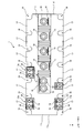
- FIG. 2 is a plan view of the semiconductor module according to the present embodiment.
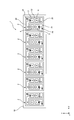
- FIG. 3 is a plan view of the semiconductor module shown in FIG. 2 with the case removed.
- the main terminal and the control terminal are omitted.
- the semiconductor modules shown below are merely examples, and the modules can be changed as appropriate without limitation.
- the longitudinal direction of the semiconductor module (direction in which a plurality of laminated substrates are lined up) is defined as the X direction
- the lateral direction of the semiconductor module is defined as the Y direction
- the height direction (thickness direction of the substrate) is defined as the Z direction.
- the illustrated X, Y, and Z axes are orthogonal to each other and form a right-handed system.
- the X direction may be referred to as a left-right direction
- the Y direction may be referred to as a front-back direction
- the Z direction may be referred to as a vertical direction.
- the heat dissipation surface side (cooler side) of the semiconductor module is referred to as the lower surface side, and the opposite side is referred to as the upper surface side.
- the plan view means the case where the upper surface of the semiconductor module is viewed from the positive side in the Z direction.
- the notation of the direction and the angle may be generally the direction and the angle, and within ⁇ 10 degrees may be allowed.
- the semiconductor module according to this embodiment is applied to a power conversion device such as a power module, and is a power module constituting an inverter circuit.
- the semiconductor module 1 includes a base plate 10, a plurality of laminated substrates 2 arranged on the base plate 10, and a plurality of semiconductor elements 3 and 4 arranged on the laminated substrate 2.
- a case 11 for accommodating the laminated substrate 2 and a plurality of semiconductor elements, and a sealing resin (not shown) filled in the case 11 are included.
- the base plate 10 is a rectangular plate having an upper surface and a lower surface.
- the base plate 10 functions as a heat sink. Further, the base plate 10 has a rectangular shape in a plan view having a long side in the X direction and a short side in the Y direction.
- the base plate 10 is a metal plate made of, for example, copper, aluminum, an alloy thereof, or the like, and the surface thereof may be plated.
- a rectangular case 11 in a plan view is arranged on the upper surface of the base plate 10.
- the case 11 is formed in a rectangular parallelepiped box shape having a frame portion forming a side wall and a lid portion covering the upper side with an opening at the lower side.
- the case 11 covers the upper part of the base plate 10 and defines a space for accommodating the laminated substrate 2, the semiconductor element, the sealing resin, and the like.
- the case 11 is provided with an external terminal.
- the external terminal is composed of a positive electrode terminal 12 (P terminal), a negative electrode terminal 13 (N terminal), and an output terminal 14 (M terminal).
- the positive electrode terminal 12, the negative electrode terminal 13, and the output terminal 14 may be referred to as a main terminal.
- the external terminal may include a plurality of control terminals 15. One end of the external terminal is connected to a predetermined circuit board inside the case 11. One end of the external terminal penetrates the case 11 and is arranged inside the case 11, and the other end is exposed to the outside (outside) from the upper surface of the case 11. The other end of the external terminal can be electrically connected to an external device.
- the other ends of the plurality of main terminals are arranged side by side in the X direction, which is the long side direction.
- the other ends of the plurality of main terminals are arranged on the upper surface of the case 11 so as to be biased toward the positive side in the X direction and in the center in the Y direction.
- the other ends of the plurality of control terminals 15 are arranged side by side in the X direction, which is the long side direction.
- the other ends of the plurality of control terminals 15 are arranged on the upper surface of the case 11 so as to be biased toward the negative side in the X direction and at the ends in the Y direction.
- a terminal arrangement portion 11a in which the main terminal is arranged and a terminal arrangement portion 11b in which the control terminal 15 is arranged are formed on the upper surface of the case 11.
- the terminal arrangement portion 11a protrudes from the upper surface of the case 11 in the Z direction and has a rectangular parallelepiped shape long in the X direction.
- the terminal arrangement portion 11a is arranged on the upper surface of the case 11 so as to be biased toward the positive side in the X direction and in the center in the Y direction.
- the terminal arrangement portion 11b is arranged on the upper surface of the protrusion 17 described below.
- the terminal arrangement portion 11b does not have to protrude in the Z direction from the upper surface of the case 11.
- the terminal arrangement portion 11b is arranged on the upper surface of the case 11 so as to be biased toward the negative side in the X direction and at the end portion in the Y direction.
- a plurality of counterbore 16s for fixing the module are formed on the pair of long sides (outer surfaces) of the cases 11 facing each other in the Y direction.
- the plurality of counterbore 16s are arranged side by side in the X direction, for example, seven per side.
- the plurality of counterbore 16s form a plurality of protrusions 17 on the side surfaces of the case 11 facing each other in the Y direction.
- a predetermined protrusion 17 located on the negative side in the X direction constitutes the terminal arrangement portion 11b. That is, the terminal arrangement portion 11b is arranged unevenly on the negative side in the X direction.
- a plurality of groove portions 11f are formed along the X direction on the pair of long sides (outer surfaces) of the cases 11 facing each other in the Y direction.
- the groove portion 11f is formed on the outer peripheral surface of a predetermined protrusion 17 and counterbore 16 in which the terminal arrangement portion 11b is arranged. That is, the groove portion 11f is unevenly arranged on the negative side in the X direction.
- one side surface 11c, 11d having a flat YZ surface is formed on a pair of short sides (outer surfaces) of the cases 11 facing each other in the X direction.
- the counterbore 16 may be formed at each of the two ends in the Y direction. That is, one side surface 11c, 11d having a flat YZ surface is formed in the center of the short side.
- a nut (both not shown) accommodating portion 18 for fixing an external conductor with a screw is formed on the upper surfaces of the terminal arrangement portions 11a and 11b.
- Six accommodating portions 18 are formed side by side in the X direction, for example.
- the accommodating portion 18 has a regular hexagonal shape in a plan view corresponding to the shape of the nut.
- a slit 19 for inserting a terminal is formed on the side of the accommodating portion 18.
- the slit 19 has a long streak in the X direction and penetrates the upper surface of the case in the thickness direction (Z direction).
- the accommodating portion 18 and the slit 19 formed in the terminal arranging portion 11b are smaller than the accommodating portion 18 and the slit 19 formed in the terminal arranging portion 11a.
- the positive electrode terminal 12, the negative electrode terminal 13, and the output terminal 14 are arranged side by side on the upper surface of the terminal arrangement portion 11a in order from the negative side in the X direction. Further, a control terminal 15 is arranged on the upper surface of the terminal arrangement portion 11b.
- One end of each terminal is inserted into the slit 19 and is joined to the laminated substrate 2 in the case 11.
- the other end side of each terminal is bent at a right angle so as to cover the upper part of the accommodating portion 18.
- a through hole is formed in the center of each of the bent terminals so as to correspond to the accommodating portion 18.
- the through port penetrates in the thickness direction (Z direction) of the terminal.
- Each external terminal is formed by pressing a metal plate such as a copper material, a copper alloy material, an aluminum alloy material, or an iron alloy material.
- the laminated substrate 2 is formed, for example, in a rectangular shape in a plan view.
- the six laminated substrates 2 are arranged side by side in the X direction.
- the laminated substrate 2 is formed by laminating a metal layer and an insulating layer, and is composed of, for example, a DCB (Direct Copper Bonding) substrate, an AMB (Active Metal Brazing) substrate, or a metal base substrate.
- the laminated substrate 2 has an insulating plate 20, a heat radiating plate (not shown) arranged on the lower surface of the insulating plate 20, and circuit boards 21, 22, and 23 arranged on the upper surface of the insulating plate 20. ..
- the insulating plate 20 has a predetermined thickness in the Z direction and is formed in a flat plate shape having an upper surface and a lower surface.
- the insulating plate 20 is a ceramic material such as alumina (Al 2 O 3 ), aluminum nitride (AlN), silicon nitride (Si 3 N 4 ), a resin material such as epoxy, or an epoxy resin material using a ceramic material as a filler. It is formed by an insulating material such as.
- the insulating plate 20 may be referred to as an insulating layer or an insulating film.
- the heat radiating plate has a predetermined thickness in the Z direction and is formed so as to cover substantially the entire lower surface of the insulating plate.
- the heat radiating plate is formed of a metal plate having good thermal conductivity such as copper or aluminum.
- three circuit plates 21, 22, and 23 are independently formed in an island shape in a state of being electrically insulated from each other. Further, in addition to the three circuit boards 21, 22, and 23, two circuit boards 24 are arranged as control circuit boards. The two circuit boards 24 are provided at a pair of corners of the insulating plates 20 that face each other at an angle. These circuit boards are composed of a metal layer having a predetermined thickness formed of copper foil or the like.
- each external terminal is connected to the upper surface of these circuit boards.
- Each end of these external terminals is directly connected to the upper surface of a predetermined circuit board by ultrasonic bonding, laser bonding, or the like, or is connected via a bonding material such as solder or sintered metal.
- the ends of each external terminal are conductively connected to a predetermined circuit board.
- the connection relationship between each external terminal and the circuit board will not be described.
- the plurality of semiconductor elements 3 and 4 are arranged on the upper surfaces of the circuit boards 21 and 22 via a joining material such as solder. As a result, the bottom electrodes of the semiconductor elements 3 and 4 are conductively connected to the circuit boards 21 and 22. By doing so, each external terminal and each semiconductor element are conductively connected.
- the semiconductor elements 3 and 4 are formed in a plan-viewing shape by, for example, a semiconductor substrate such as silicon (Si), silicon carbide (SiC), or gallium nitride (GaN).
- a semiconductor substrate such as silicon (Si), silicon carbide (SiC), or gallium nitride (GaN).
- switching elements such as an IGBT (Insulated Gate Bipolar Transistor) and a power MOSFET (Metal Oxide Semiconductor Field Effect Transistor), and a diode such as an FWD (Free Wheeling Diode) are used.
- IGBT Insulated Gate Bipolar Transistor
- MOSFET Metal Oxide Semiconductor Field Effect Transistor
- FWD Free Wheeling Diode
- the semiconductor element even if an RC (Reverse Conducting) -IGBT element in which an IGBT and an FWD are integrated, a power MOSFET element, an RB (Reverse Blocking) -IGBT having a sufficient withstand voltage against a reverse bias, or the like is used. good.
- the shape, number of arrangements, arrangement locations, etc. of the semiconductor element can be changed as appropriate.
- the semiconductor element in the present embodiment is a vertical switching element in which a functional element such as a transistor is formed on a semiconductor substrate.
- semiconductor elements 3 and 4 are arranged one by one in the Y direction on the upper surface of the circuit board 21.
- the semiconductor element 3 is located on the positive side in the Y direction, and the semiconductor element 4 is located on the negative side in the Y direction.
- semiconductor elements 3 and 4 are arranged one by one in the Y direction on the upper surface of the circuit board 22.
- the semiconductor element 4 is located on the positive side in the Y direction, and the semiconductor element 3 is located on the negative side in the Y direction.
- the semiconductor elements 3 and 4 on the circuit board 21 form the upper arm
- the semiconductor elements 3 and 4 on the circuit board 22 form the lower arm.
- the semiconductor elements 3 and 4 arranged in the Y direction are electrically connected by a wiring member. Further, the semiconductor element 4 and the predetermined circuit board are electrically connected by a wiring member. Further, the gate electrode of the semiconductor element 3 and the circuit board 24 are electrically connected by a wiring member.
- Conductor wires are used for these wiring members.
- the material of the conductor wire any one of gold, copper, aluminum, gold alloy, copper alloy, aluminum alloy or a combination thereof can be used. It is also possible to use a member other than the conductor wire as the wiring member. For example, a ribbon can be used as the wiring member.
- the wiring member is not limited to a wire or the like, and may be formed of a metal plate such as a copper material, a copper alloy-based material, an aluminum alloy-based material, or an iron alloy-based material.
- a product is produced by the following steps. (1) Resin pellets, which are the material of the case, are supplied into the cylinder of the molding machine. (2) The resin is plasticized (melted) by being heated in the cylinder. (3) By rotating the screw in the cylinder, the resin is injected into the mold at high temperature and high pressure. (4) The resin is pressurized, cooled, and solidified in the mold, and then the mold is opened and the molded product is taken out by an ejector pin or the like. (5) An unnecessary part (resin flow path part, etc.) of the molded product is cut to obtain a product.
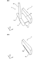
- FIG. 4 is a perspective view of the periphery of the gate of the case according to the reference example.
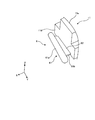
- FIG. 5 is a perspective view of the periphery of the gate of the case according to the present embodiment.
- FIG. 6 is a cross-sectional view of the periphery of the gate of the case according to the present embodiment.
- 4A, 5A, and 6A show the state immediately after the molded product is taken out from the mold.
- 4B, 5B, and 6B show a state in which an unnecessary portion (resin flow path portion) is cut from the molded product.
- the resin passage from the injection molding machine to the mold remains as an unnecessary portion (resin flow path portion 5).
- the resin flow path portion 5 includes a sprue portion 50 connected to the injection molding machine, a runner portion 51 connected to the sprue portion 50, and a pair of gate portions 52 connecting the runner portion 51 and the case 11. Will be done.
- the sprue portion 50 is a passage for transferring the resin from the nozzle of the injection molding machine to the runner portion 51.
- the sprue portion 50 has a cylindrical shape extending in the Z direction. Further, the sprue portion 50 has a tapered shape so as to gradually increase in diameter from the upper end side to the lower end side. The lower end of the sprue portion 50 penetrates the runner portion 51.
- the runner portion 51 is a passage for guiding the resin from the sprue portion 50 into the mold (cavity).
- the runner section 51 has a first runner section 51a and a pair of second runner sections 51b.
- the first runner portion 51a has a cylindrical shape extending from the lower end side of the sprue portion 50 to both sides in the Y direction.
- the first runner portion 51a has a length corresponding to the width of the case 11 in the Y direction.
- the pair of second runner portions 51b each have a cylindrical shape extending from both ends of the first runner portion 51a toward the positive side in the X direction.
- the second runner portion 51b extends toward one side surface 11c of the case 11.
- the gate portion 52 is a passage connecting the runner portion 51 (second runner portion 51b) and the mold, and constitutes an inlet of the resin to the mold.
- the gate portion 52 has a prismatic shape extending from the tip of each second runner portion 51b toward one side surface 11c of the case 11.
- the gate portion 52 has a rectangular cross section smaller than the outer diameter of the second runner portion 51b.
- two gate portions 52 having a relatively small cross-sectional area are provided. Therefore, in the case of a relatively large case, there is a possibility that a sufficient amount of resin cannot be filled when the resin is injected into the mold. Further, since there are a plurality of gate portions 52, a confluence portion between the resins that have entered from each of the gate portions 52 is generated in the mold. The confluence of the resins can later become a location that affects the strength of the case.
- burrs which are the remaining portions of the gate portion 52, protrude from one side surface 11c of the case 11 at a predetermined height.
- the height of the burr is 0.5 mm to 2.0 mm. This burr may interfere with a dedicated jig in a later assembly process and cause a component mounting defect, so it is preferable that the burr is as small as possible. In particular, it is preferable that the protruding height of the burr is small.
- the runner portion 51 forming a part of the resin passage has a film shape.
- the resin flow path portion 5 includes a sprue portion 50 connected to the injection molding machine, a runner portion 51 connected to the sprue portion 50, and a gate portion 52 connecting the runner portion 51 and the case 11. (First gate portion) and. Since the sprue portion 50 has the same configuration as that of FIG. 4, the description thereof will be omitted.
- the runner portion 51 is a passage for guiding the resin from the sprue portion 50 into the mold (cavity).
- the runner section 51 has a first runner section 51a and a second runner section 51b.
- the first runner portion 51a has a cylindrical shape extending from the lower end side of the sprue portion 50 to both sides in the Y direction.
- the first runner portion 51a has a length corresponding to the width of the case 11 in the Y direction.
- the second runner portion 51b extends like a film from the side surface of the first runner portion 51a toward one side surface 11c of the case 11 on the positive side in the X direction.
- the second runner portion 51b is long in the width direction (Y direction) of the case 11 and has a thickness in the Z direction.
- the second runner portion 51b has a tapered shape that is inclined so that the thickness decreases toward the positive side in the X direction (the gate portion 52 side described later). This inclination angle is, for example, around 15 degrees.
- the gate portion 52 is a passage connecting the runner portion 51 (second runner portion 51b) and the mold, and constitutes an inlet of the resin to the mold.
- the gate portion 52 has a long flat shape in the width direction (Y direction) of the case 11.
- the case 11 after removing the resin flow path portion 5 includes a cross section 52a of a single gate portion 52 on one side surface 11c of the case 11.
- the gate portion 52 after removing the resin flow path portion 5 may be a portion having a large surface roughness with respect to one side surface 11c of the case 11.
- burrs which are the remaining portions of the gate portion 52, may protrude from one side surface 11c of the case 11 at a predetermined height.
- the height of the burr in this case is, for example, less than 0.5 mm.
- the gate portion 52 after removing the resin flow path portion 5 may be recessed from one side surface 11c of the case 11 to the inner surface side of the case to a predetermined depth.
- the depth of scooping in this case is, for example, less than 0.5 mm.
- the manufacturing method of the case 11 includes a step (filling step) of filling the mold with the resin through the resin passages (sprue portion 50, runner portion 51, gate portion 52) described above, and a mold.
- the second runner portion 51b has a long film shape in the width direction of the case 11. Further, the gate portion 52 has a flat shape long in the width direction of the case 11 by being connected to the second runner portion 51b.
- the flat gate portion 52 having a larger cross-sectional area than the reference example it is possible to fill the mold with a large amount of resin in a short time. Further, as compared with the reference example in which a plurality of gate portions 52 are provided, by using a single gate portion 52 in the present embodiment, it is possible to reduce the number of welded portions where the resins merge in the mold. be. As a result, it is possible to sufficiently secure the strength of the molded product (case 11).
- one flat side surface 11c, 11d is formed in a YZ plane corresponding to the short side.
- One side surfaces 11c and 11d face each other in the X direction.
- one side surface 11c and 11d are formed in the center of the short side.
- a single gate portion 52 is formed in the center of the lower edge portion of one side surface 11c having a flat YZ surface.
- a single gate portion 52 is arranged at the center of the lower edge portion of one side surface 11c on the short side of the case 11. Therefore, the resin can flow in uniformly without bias, the number of welded portions can be reduced, and a case having uniform characteristics can be manufactured. Further, the gate portion 52 is formed on a flat surface. Therefore, unnecessary parts of the molded product can be easily removed.
- a plurality of groove portions 11f are formed on the side surfaces of the pair of long sides along the X direction.
- the groove portion 11f is also formed in a predetermined protrusion 17 and counterbore 16 in which the terminal arrangement portion 11b is arranged.
- the main terminals (positive electrode terminal 12, negative electrode terminal 13, and output terminal 14) are arranged on the positive side in the X direction, which is one end side, and the control terminal 15 is arranged on the negative side in the X direction, which is the other end side.
- the single gate portion 52 is provided on one side surface 11c located on the other end side of the case 11.
- the resin inlet is provided on the control terminal 15 side, which has a relatively complicated case shape as compared with the main terminal side. Since the temperature of the resin is relatively high and the viscosity is low on the inlet side, it is possible to obtain a good molded product by arranging the complicated shape of the case 11 on the inlet side.
- the main terminal side which is relatively far from the inlet, has a relatively simple shape even if the temperature of the resin decreases and the viscosity increases to some extent, so that there is no problem in moldability.
- the thickness (length in the Z direction) of the gate portion 52 is preferably 0.5 mm or more and 2.5 mm or less.
- the thickness of the gate portion 52 (length in the Z direction) is preferably 1/100 times or more and 1/10 times or less the width of the gate portion 52 (length in the Y direction).
- the second runner portion 51b has a long film shape in the width direction of the case 11, and is inclined so that the thickness decreases toward the gate portion 52 side.
- the inclination angle is preferably, for example, 10 degrees or more and 30 degrees or less. According to these configurations, the proximal end side of the second runner portion 51b is thicker than the gate portion 52 side, so that the rigidity of the proximal end side is increased.
- the gate portion 52 has a smaller thickness (length in the Z direction) than the length (length in the Y direction), and is thinner than the base end side of the second runner portion 51b. Therefore, the rigidity in the Z direction (shear rigidity) is small. As a result, by applying a force in the Z direction when removing the resin flow path portion 5, it is possible to facilitate cutting starting from the gate portion 52. Further, the protruding height of the cross section of the gate portion 52 (height from one side surface 11c of the case 11) can be reduced, and the removal process of the end surface of the gate portion 52 can be simplified.
- the resin constituting the case 11 is a thermoplastic resin.
- resins include polyphenylene succide (PPS) resin, polybutylene terephthalate (PBT) resin, polybutylene succinate (PBS) resin, polyamide (PA) resin, and acrylonitrile butadiene styrene (ABS) resin.
- PPS polyphenylene succide
- PBT polybutylene terephthalate
- PBS polybutylene succinate
- PA polyamide
- ABS acrylonitrile butadiene styrene
- a filler may be added to the resin.
- the filler is, for example, ceramics.
- Such fillers include silicon oxide, aluminum oxide, boron nitride or aluminum nitride.
- the case 11 is preferably made of a polyamide resin such as nylon 6 or nylon 66 containing any of the fillers.
- the gate portion 52 is provided on the lower edge portion of the case 11. By locating the gate portion 52 at the end of the case 11, it is possible to prevent the case 11 from being cracked from the gate portion 52 as a starting point.
- the lower edge portion of the case 11 is provided with a protrusion 11e protruding downward.
- the protrusion 11e is formed in a rectangular frame shape along the outer shape of the case 11.
- the gate portion 52 is formed above the protrusion portion 11e. More specifically, the lower surface of the gate portion 52 is flush with the base end (lower surface of the case 11) of the protrusion 11e.
- the protrusion 11e has a shape along the outer shape of the base plate 10 and functions as a protrusion for positioning the case 11 with respect to the base plate 10.
- a resin pool 6 corresponding to the resin outlet is formed on one side surface 11d located on one end side of the case 11.
- the resin flow path portion 5 and the resin pool 6 are provided at symmetrical positions with the case 11 interposed therebetween in the X direction.
- the resin pool 6 includes a runner portion 61 (another runner portion) and a single gate portion 62 (second gate portion) that connects the runner portion 61 and the case 11.
- the single gate portion 62 (second gate portion) is formed in the center of the lower edge portion of one side surface 11d having a flat YZ surface. According to this configuration, a single gate portion 62 is arranged at the center of the lower edge portion of one side surface 11c on the short side of the case 11. Further, the gate portion 62 is provided at a symmetrical position of the gate portion 52 with the case 11 interposed therebetween in the X direction. Therefore, it is possible to uniformly flow out the unnecessary resin without bias, reduce the number of welded portions, and manufacture a case having uniform characteristics. Further, the gate portion 62 is formed on a flat surface (one side surface 11d). Therefore, unnecessary parts of the molded product can be easily removed.
- the runner portion 61 is configured to include a portion for removing air entrained by the resin at the beginning of injection.
- the runner section 61 has a first runner section 61a and a second runner section 61b.
- the first runner portion 61a has a cylindrical shape extending on both sides in the Y direction at a position facing one side surface 11d of the case 11.
- the first runner portion 61a has a length corresponding to the width of the case 11 in the Y direction.
- the second runner portion 61b extends like a film from the side surface of the first runner portion 61a toward one side surface 11d of the case 11 on the negative side in the X direction.
- the second runner portion 61b is long in the width direction (Y direction) of the case 11 and has a thickness in the Z direction. Further, the second runner portion 61b has a tapered shape that is inclined so that the thickness decreases toward the negative side in the X direction (the gate portion 62 side described later).
- the inclination angle is preferably 10 degrees or more and 30 degrees or less.
- the gate portion 62 is a passage connecting the runner portion 61 (second runner portion 61b) and the mold, and constitutes a resin outlet for the mold.
- the gate portion 62 has a flat shape that is long in the width direction (Y direction) of the case 11.
- the thickness (length in the Z direction) of the gate portion 62 is preferably 0.5 mm or more and 2.5 mm or less.
- the thickness of the gate portion 62 (the length in the Z direction) and the width of the gate portion 62 (the length in the Y direction) are preferably 1/100 times or more and 1/10 times or less.
- the gate portion 62 and the runner portion 61 described above form a resin discharge passage for discharging the resin entrained with air at the beginning of injection to the outside of the case 11. According to the gate portion 62 and the runner portion 61, even if air is caught in the case 11, it is possible to obtain a good molded product with the air removed as a product.
- the thickness (length in the Z direction) is smaller than the length (length in the Y direction), and the base end side of the second runner portion 61b is smaller than the gate portion 62 side. It gets thicker. Therefore, the rigidity of the base end side is increased.
- the gate portion 62 is thinner than the proximal end side of the second runner portion 61b, the rigidity in the Z direction is small. As a result, by applying a force in the Z direction when removing the resin flow path portion 6, it is possible to facilitate cutting starting from the gate portion 62.
- the second runner portion 61b on the exit side is shorter than the second runner portion 51b on the entrance side. This is because the second runner portion 61b becomes an unnecessary portion as a part of the resin flow path portion 6 in the first place, so that the shorter one is economical because the amount of resin used is reduced.
- the number and layout of the circuit boards are not limited to the above configuration and can be changed as appropriate.
- the case 11 is formed in a box shape having an opening below the base plate 10 and below so as to cover the plurality of semiconductor elements, but the configuration is not limited to this.
- the case 11 may have a frame-shaped configuration in which the lower part and the upper part are opened.
- the case lid may be arranged so as to cover the opening above the case 11.
- the case 11 is arranged on the upper surface of the base plate 10, but the configuration is not limited to this.
- the case 11 may be arranged on the upper surface of the laminated substrate 2 without the base plate 10.
- the laminated substrate 2 and the semiconductor element are formed in a rectangular shape or a rectangular shape in a plan view, but the configuration is not limited to this.
- the laminated substrate 2 and the semiconductor element may be formed in a polygonal shape other than the above.
- the present embodiment is not limited to the above-described embodiment and modification, and may be variously changed, replaced, or modified without departing from the spirit of the technical idea. Further, if the technical idea can be realized in another way by the advancement of the technology or another technology derived from it, it may be carried out by the method. Therefore, the claims cover all embodiments that may be included within the scope of the technical idea.
- the case of the semiconductor module according to the above embodiment is a case of a semiconductor module that houses a semiconductor element and is formed by injection molding in a box shape with an opening at the bottom, has a rectangular shape in a plan view, and has an upper surface.
- an external terminal is arranged on the side surface, and the external terminal is electrically connected to the semiconductor element inside the case, penetrates the inside and the outside of the case, and corresponds to a rectangular short side.
- a single first gate portion, which is an inlet for the resin, is provided on the side surface, and the first gate portion has a flat shape long in the width direction of the case.
- the main terminal is arranged on one end side of the rectangular shape
- the control terminal is arranged on the other end side
- the first gate portion is on the other end side. It is placed on one side.
- a plurality of grooves are formed along the longitudinal direction on the side surface corresponding to the long side of the rectangular shape.
- the width is 1/100 times or more and 1/10 times or less the width of the first gate portion.
- the resin is formed of a polyamide resin to which a filler is added.
- the first gate portion is provided on the lower edge portion of the case.
- the lower edge portion of the case has a protrusion protruding downward, and the first gate portion is formed above the protrusion.
- a single second gate portion which is an outlet of the resin is further provided on one side surface located on the one end side, and the second gate portion is the case. It has a long flat shape in the width direction of.
- the second gate portion is provided at a symmetrical position with respect to the first gate portion.
- the method for manufacturing a case of a semiconductor module includes a step of filling a mold with a resin through the first gate portion, a step of removing a resin flow path portion connected to the case, and a step of removing the resin flow path portion connected to the case.
- the resin flow path portion has a runner portion that is connected to the first gate portion to form the resin passage, and the runner portion has a film shape that is long in the width direction of the case. It is inclined so that the thickness decreases toward the first gate portion side.
- the inclination angle of the runner portion is 10 degrees or more and 30 degrees or less.
- a single second gate portion which is an outlet for the resin, is provided on one side surface located on one end side thereof, and the second gate is provided.
- the portion has a flat shape that is long in the width direction of the case, and the resin flow path portion includes another runner portion that is connected to the second gate portion to form the resin passage, and the other runner portion.
- Has a long film shape in the width direction of the case, is inclined so that the thickness becomes smaller toward the second gate portion side, and is shorter than the runner portion.
- the present invention has the effect that a sufficient amount of resin can be supplied into the mold even in a short time to obtain a good molded product, and in particular, the case of a semiconductor module. And useful for manufacturing methods of semiconductor module cases.
Landscapes
- Engineering & Computer Science (AREA)
- Manufacturing & Machinery (AREA)
- Mechanical Engineering (AREA)
- Moulds For Moulding Plastics Or The Like (AREA)
- Injection Moulding Of Plastics Or The Like (AREA)
- Structures Or Materials For Encapsulating Or Coating Semiconductor Devices Or Solid State Devices (AREA)
- Encapsulation Of And Coatings For Semiconductor Or Solid State Devices (AREA)
Abstract
短時間であっても金型内に十分な量の樹脂を供給して良好な成型品を得ること。半導体モジュールのケース(11)は、半導体素子を収容し、下方が開口された箱型で射出成型により形成されている。ケースは、平面視矩形状を有し、上面又は側面に外部端子が配置されている。外部端子は、ケースの内側で半導体素子と電気的に接続され、ケースの内側と外側を貫通している。ケースは、矩形状の短辺に対応する一側面に樹脂の入口である単一の第1ゲート部(52)を備えている。第1ゲート部は、ケースの幅方向に長い扁平形状を有している。
Description
本発明は、半導体モジュールのケース及び半導体モジュールのケースの製造方法に関する。
半導体装置は、IGBT(Insulated Gate Bipolar Transistor)、パワーMOSFET(Metal Oxide Semiconductor Field Effect Transistor)、FWD(Free Wheeling Diode)等の半導体素子が設けられた基板を有し、インバータ装置等に利用されている。
この種の半導体モジュールにおいて、所定の基板上に配置された半導体素子は、例えば樹脂製のケースに収容される。半導体モジュールで使用されるケースの量産には、例えば射出成型技術が用いられる。射出成型では、加温溶融された樹脂を金型内に射出し、加圧、冷却、固化等の工程を経て所望の成型品がつくられる(例えば、特許文献1-4参照)。
ところで、大容量の半導体モジュールにおいては、ケースの大型化によって、成型時により多くの樹脂を短時間で供給する必要がある。例えば、短時間の射出によって金型内における樹脂の充填量が少なすぎると、成型品の肉厚を十分に確保できずに不良が発生する可能性がある。また、樹脂の充填量を確保するために射出速度を速めることも考えられる。しかしながら、樹脂の射出速度が速すぎると、樹脂が金型内のエアを巻き込んでしまい樹脂ボイドが発生する要因となる。このように、ケースの大型化に伴う射出成型の条件変更には、様々な制約が伴うおそれがあった。
本発明はかかる点に鑑みてなされたものであり、短時間であっても金型内に十分な量の樹脂を供給して良好な成型品を得ることが可能な半導体モジュールのケース及び半導体モジュールのケースの製造方法を提供することを目的の1つとする。
本発明の一態様の半導体モジュールのケースは、半導体素子を収容し、下方が開口された箱型で射出成型により形成された半導体モジュールのケースであって、平面視矩形状を有し、上面又は側面に外部端子が配置され、前記外部端子は、前記ケースの内側で前記半導体素子と電気的に接続され、前記ケースの内側と外側を貫通しており、矩形状の短辺に対応する一側面に樹脂の入口である単一の第1ゲート部を備え、前記第1ゲート部は、前記ケースの幅方向に長い扁平形状を有する。
本発明の一態様の上記の半導体モジュールのケースの製造方法は、前記第1ゲート部を通じて金型内に樹脂を充填する工程と、前記ケースに連なった樹脂流路部分を除去する工程と、を備え、前記樹脂流路部分は、前記第1ゲート部に連なって前記樹脂の通路を形成するランナー部を有し、前記ランナー部は、前記ケースの幅方向に長いフィルム形状を有し、前記第1ゲート部側に向かうにしたがって厚みが小さくなるように傾斜している。
本発明によれば、短時間であっても金型内に十分な量の樹脂を供給して良好な成型品を得ることが可能である。
以下、本発明を適用可能な半導体モジュールについて説明する。図1は、本実施の形態に係る半導体モジュールの斜視図である。図2は、本実施の形態に係る半導体モジュールの平面図である。図3は、図2に示す半導体モジュールからケースを取り外した平面図である。図2及び図3では、説明の便宜上、主端子及び制御端子を省略している。なお、以下に示す半導体モジュールはあくまで一例にすぎず、これに限定されることなく適宜変更が可能である。
また、以下の図において、半導体モジュールの長手方向(複数の積層基板が並ぶ方向)をX方向、半導体モジュールの短手方向をY方向、高さ方向(基板の厚み方向)をZ方向と定義することにする。図示されたX、Y、Zの各軸は互いに直交し、右手系を成している。また、場合によっては、X方向を左右方向、Y方向を前後方向、Z方向を上下方向と呼ぶことがある。これらの方向(前後左右上下方向)は、説明の便宜上用いる文言であり、半導体モジュールの取付姿勢によっては、XYZ方向のそれぞれとの対応関係が変わることがある。例えば、半導体モジュールの放熱面側(冷却器側)を下面側とし、その反対側を上面側と呼ぶことにする。また、本明細書において、平面視は、半導体モジュールの上面をZ方向正側からみた場合を意味する。また、本明細書において、方向や角度の表記は、概ねその方向や角度であればよく、±10度以内は許容されてよいものとする。
本実施の形態に係る半導体モジュールは、例えばパワーモジュール等の電力変換装置に適用されるものであり、インバータ回路を構成するパワーモジュールである。図1-3に示すように、半導体モジュール1は、ベース板10と、ベース板10上に配置される複数の積層基板2と、積層基板2上に配置される複数の半導体素子3、4と、積層基板2及び複数の半導体素子を収容するケース11と、ケース11内に充填される封止樹脂(不図示)と、を含んで構成される。
ベース板10は、上面と下面を有する長方形の板である。ベース板10は、放熱板として機能する。また、ベース板10は、X方向に長辺、Y方向に短辺を備える平面視矩形状を有している。ベース板10は、例えば銅、アルミニウム又はこれらの合金等からなる金属板であり、表面にメッキ処理が施されてもよい。
ベース板10の上面には、平面視矩形状のケース11が配置される。ケース11は、下方が開口され、側壁を形成する枠部と上方を覆う蓋部とを有する直方体の箱型に形成されている。ケース11は、ベース板10の上方を覆い、積層基板2、半導体素子、封止樹脂等を収容する空間を画定する。
また、ケース11には、外部端子が設けられている。具体的に外部端子は、正極端子12(P端子)と、負極端子13(N端子)と、出力端子14(M端子)と、によって構成される。正極端子12、負極端子13、及び出力端子14は、主端子と呼ばれてもよい。また、外部端子には、複数の制御端子15が含まれてよい。外部端子の一端は、ケース11の内部で所定の回路板に接続されている。外部端子は、ケース11を貫通して、一端がケース11の内側に配置され、他端がケース11の上面から外部(外側)に露出されている。外部端子の他端は、外部機器に電気的に接続することができる。複数の主端子(正極端子12、負極端子13、出力端子14)の他端は、長辺方向であるX方向に並んで配置されている。複数の主端子の他端は、ケース11の上面において、X方向正側に偏って且つY方向中央に配置されている。複数の制御端子15の他端は、長辺方向であるX方向に並んで配置されている。複数の制御端子15の他端は、ケース11の上面において、X方向負側に偏って且つY方向端部に配置されている。
具体的にケース11の上面には、主端子が配置される端子配置部11aと、制御端子15が配置される端子配置部11bと、が形成されている。端子配置部11aは、ケース11の上面からZ方向に突出し、X方向に長い直方体形状を有している。端子配置部11aは、ケース11の上面において、X方向正側に偏って且つY方向中央に配置されている。
端子配置部11bは、次に記載する突起部17の上面に配置されている。端子配置部11bは、ケース11の上面からZ方向に突出していなくてもよい。端子配置部11bは、ケース11の上面において、X方向負側に偏って且つY方向端部に配置されている。
また、Y方向で対向するケース11の一対の長辺(外側面)には、モジュール固定用の複数の座ぐり16が形成されている。複数の座ぐり16は、X方向に並んで例えば一辺につき7つずつ配置されている。複数の座ぐり16によって、Y方向で対向するケース11の側面には、複数の突起部17が形成される。複数の突起部17のうち、X方向負側に位置する所定の突起部17は、端子配置部11bを構成する。すなわち、端子配置部11bは、X方向負側に偏って配置されている。
また、Y方向で対向するケース11の一対の長辺(外側面)には、X方向に沿って複数の溝部11fが形成されている。溝部11fは、端子配置部11bが配置された所定の突起部17及び座ぐり16の外周面に形成されている。すなわち、溝部11fは、X方向負側に偏って配置されている。
また、X方向で対向するケース11の一対の短辺(外側面)には、平坦なYZ面を有する一側面11c,11dが形成されている。また、Y方向の2つの端部にそれぞれ座ぐり16が形成されていてよい。すなわち、平坦なYZ面を有する一側面11c,11dは、短辺の中央に形成されている。
図2に示すように、端子配置部11a、11bの上面には、外部導体をネジで固定するナット(共に不図示)の収容部18が形成されている。収容部18は、X方向に並んで例えば6つ形成されている。収容部18は、ナットの形状に対応して平面視正六角形状を有している。また、収容部18の側方には、端子挿入用のスリット19が形成されている。スリット19は、X方向に長い筋状でケースの上面を厚み方向(Z方向)に貫通している。また、端子配置部11bに形成された収容部18及びスリット19は、端子配置部11aに形成された収容部18及びスリット19より小さい。
図1に示すように、端子配置部11aの上面には、X方向負側から順に、正極端子12、負極端子13、及び出力端子14が並んで配置されている。また、端子配置部11bの上面には、制御端子15が配置されている。各端子は、一端側がスリット19に挿入され、ケース11内で積層基板2に接合されている。各端子の他端側は、収容部18の上方を覆うように直角に折り曲げられている。折り曲げられた各端子の中央には、収容部18に対応して貫通口が形成されている。貫通口は、端子の厚み方向(Z方向)に貫通している。各外部端子は、銅素材、銅合金系素材、アルミニウム合金系素材、鉄合金系素材等の金属板をプレス加工等して形成されている。
また、図3に示すように、ケース11の内側において、ベース板10の上面には、6つの積層基板2が配置されている。積層基板2は、例えば平面視矩形状に形成されている。6つの積層基板2は、X方向に並んで配置されている。積層基板2は、金属層と絶縁層とを積層して形成され、例えば、DCB(Direct Copper Bonding)基板やAMB(Active Metal Brazing)基板、あるいは金属ベース基板で構成される。具体的に積層基板2は、絶縁板20と、絶縁板20の下面に配置された放熱板(不図示)と、絶縁板20の上面に配置された回路板21、22、23と、を有する。
絶縁板20は、Z方向に所定の厚みを有し、上面と下面を有する平板状に形成される。絶縁板20は、例えばアルミナ(Al2O3)、窒化アルミニウム(AlN)、窒化珪素(Si3N4)等のセラミックス材料、エポキシ等の樹脂材料、又はセラミックス材料をフィラーとして用いたエポキシ樹脂材料等の絶縁材料によって形成される。なお、絶縁板20は、絶縁層又は絶縁フィルムと呼ばれてもよい。
放熱板は、Z方向に所定の厚みを有し、絶縁板の下面の略全体を覆うように形成される。放熱板は、例えば銅やアルミニウム等の熱伝導性の良好な金属板によって形成される。
絶縁板20の上面(主面)には、3つの回路板21、22、23が、電気的に互いに絶縁された状態で、独立して島状に形成されている。また、3つの回路板21、22、23の他に、制御用の回路板として、2つの回路板24が配置されている。2つの回路板24は、斜めで対向する絶縁板20の一対の角部に設けられている。これらの回路板は、銅箔等によって形成される所定厚みの金属層で構成される。
これらの回路板の上面には、上記した外部端子の端部が接続される。これらの外部端子は、それぞれの端部が所定の回路板の上面に、超音波接合やレーザ接合等で直接接続、又は、半田や焼結金属等の接合材を介して接続されている。これにより、各外部端子の端部が、所定の回路板に導電接続される。便宜上、各外部端子と回路板との接続関係は、説明を省略する。
複数の半導体素子3、4は、半田等の接合材を介して回路板21、22の上面に配置されている。これにより、半導体素子3、4の各下面電極が回路板21、22に導電接続される。そうすることで、各外部端子と各半導体素子が導電接続されている。
半導体素子3、4は、例えばシリコン(Si)、炭化けい素(SiC)、窒化ガリウム(GaN)等の半導体基板によって平面視方形状に形成される。なお、半導体素子3、4としては、IGBT(Insulated Gate Bipolar Transistor)、パワーMOSFET(Metal Oxide Semiconductor Field Effect Transistor)等のスイッチング素子、FWD(Free Wheeling Diode)等のダイオードが用いられる。以下、本実施の形態では、一方の半導体素子3をIGBT素子とし、他方の半導体素子4をダイオード素子とする。また、半導体素子として、IGBTとFWDを一体化したRC(Reverse Conducting)-IGBT素子、又はパワーMOSFET素子、逆バイアスに対して十分な耐圧を有するRB(Reverse Blocking)-IGBT等が用いられてもよい。また、半導体素子の形状、配置数、配置箇所等は適宜変更が可能である。なお、本実施の形態における半導体素子は、半導体基板にトランジスタなどの機能素子を形成した、縦型のスイッチング素子である。
本実施の形態では、回路板21の上面に半導体素子3、4が1つずつY方向に並んで配置されている。回路板21では、Y方向正側に半導体素子3が位置し、Y方向負側に半導体素子4が位置している。回路板22の上面にも同様に、半導体素子3、4が1つずつY方向に並んで配置されている。回路板22では、Y方向正側に半導体素子4が位置し、Y方向負側に半導体素子3が位置している。本実施の形態では、回路板21上の半導体素子3、4が上アームを構成し、回路板22上の半導体素子3、4が下アームを構成する。
また、Y方向に並んだ半導体素子3、4は、配線部材によって電気的に接続される。また半導体素子4と所定の回路板とは、配線部材によって電気的に接続される。また、半導体素子3のゲート電極と回路板24とは、配線部材によって電気的に接続される。
これらの配線部材には、導体ワイヤ(ボンディングワイヤ)が用いられる。導体ワイヤの材質は、金、銅、アルミニウム、金合金、銅合金、アルミニウム合金のいずれか1つ又はそれらの組み合わせを用いることができる。また、配線部材として導体ワイヤ以外の部材を用いることも可能である。例えば、配線部材としてリボンを用いることができる。また、配線部材は、ワイヤ等に限らず、銅素材、銅合金系素材、アルミニウム合金系素材、鉄合金系素材等の金属板によって形成されてもよい。
ところで、上記したように半導体モジュールのケース(端子ケースと呼ばれてもよい)の量産には、射出成型技術が用いられる。この種の射出成型では、例えば以下の工程によって製品がつくられる。
(1)ケースの材料である樹脂ペレットが成型機のシリンダ内に供給される。
(2)シリンダ内で樹脂が加温されることにより、樹脂は可塑化(溶融化)する。
(3)シリンダ内のスクリューが回転されることにより、樹脂が高温・高圧の状態で金型内に射出される。
(4)樹脂は、金型内で加圧、冷却、固化され、その後、金型を開いてエジェクタピンなどによって成型品が取り出される。
(5)成型品の不要部分(樹脂流路部分等)をカットして製品を得る。
(1)ケースの材料である樹脂ペレットが成型機のシリンダ内に供給される。
(2)シリンダ内で樹脂が加温されることにより、樹脂は可塑化(溶融化)する。
(3)シリンダ内のスクリューが回転されることにより、樹脂が高温・高圧の状態で金型内に射出される。
(4)樹脂は、金型内で加圧、冷却、固化され、その後、金型を開いてエジェクタピンなどによって成型品が取り出される。
(5)成型品の不要部分(樹脂流路部分等)をカットして製品を得る。
また、大容量の半導体モジュールにおいては、ケースの大型化によって、成型時により多くの樹脂を短時間で供給する必要がある。成形時間を長くしてしまうと、タクトタイムの増加によってコストアップの要因となる他、溶融した樹脂の温度が低下して流動性が悪くなり、成型不良の要因とも成り得る。すなわち、成型品を低コストで品質よく生産するためには、成形時間を短時間にする必要がある。
タクトタイムを短くするために、例えば、樹脂の射出時間を短くすることが考えられる。しかしながら、金型内における樹脂の充填量が少なすぎる結果、成型品の肉厚を十分に確保できずに不良が発生する可能性がある。また、樹脂の充填量を確保するために射出速度を速めることも考えられる。しかしながら、樹脂の射出速度が速すぎると、樹脂が金型内のエアを巻き込んでしまい樹脂ボイドが発生する要因となる。また、金型の保圧時間(加圧時間)が短すぎると、樹脂が十分に固化せずに逆流してヒケ等が発生するおそれがある。このように、ケースの大型化に伴う射出成型の条件変更には、様々な制約が伴うおそれがあった。
そこで、本件発明者は、ケース金型に対する樹脂の入口であるゲートの形状に着目し、本発明に想到した。ここで、図4から図6を参照して、本実施の形態に係る半導体モジュールのケース及びケースの製造方法について詳細に説明する。図4は、参考例に係るケースのゲート周辺の斜視図である。図5は、本実施の形態に係るケースのゲート周辺の斜視図である。図6は、本実施の形態に係るケースのゲート周辺の断面図である。図4A、図5A、及び図6Aは、成型品を金型から取り出した直後の状態を示している。図4B、図5B、及び図6Bは、成型品から不要部分(樹脂流路部分)をカットした状態を示している。
図4Aに示すように、参考例に係る成型品には、射出成型機から金型(共に不図示)までの樹脂の通路が不要部分(樹脂流路部分5)として残っている。具体的に樹脂流路部分5は、射出成型機に連なるスプルー部50と、スプルー部50に連なるランナー部51と、ランナー部51及びケース11を連結する一対のゲート部52と、を含んで構成される。
スプルー部50は、射出成型機のノズルからランナー部51まで樹脂を移送するための通路である。具体的にスプルー部50は、Z方向に延びる円柱形状を有している。また、スプルー部50は、上端側から下端側に向かって徐々に拡径するようにテーパ形状を有している。スプルー部50の下端は、ランナー部51を貫通している。
ランナー部51は、スプルー部50から金型内(キャビティ)に樹脂を導く通路である。具体的にランナー部51は、第1ランナー部51aと、一対の第2ランナー部51bと、を有している。第1ランナー部51aは、スプルー部50の下端側からY方向両側に延びる円柱形状を有している。第1ランナー部51aは、ケース11のY方向の幅に対応した長さを有している。一対の第2ランナー部51bは、第1ランナー部51aの両端からそれぞれX方向正側に向かって延びる円柱形状を有している。第2ランナー部51bは、ケース11の一側面11cに向かって延びている。
ゲート部52は、ランナー部51(第2ランナー部51b)と金型とを接続する通路であり、金型に対する樹脂の入口を構成する。具体的にゲート部52は、各第2ランナー部51bの先端からケース11の一側面11cに向かって延びる角柱形状を有している。また、ゲート部52は、第2ランナー部51bの外径よりも小さい矩形断面を有している。例えば、ゲート部52一つ当たりの断面積は、3mm×5mm=15mm2である。
図4に示す参考例では、上記したように、比較的断面積の小さいゲート部52が2つ設けられている。このため、比較的大型のケースの場合には、金型内に樹脂を射出する際に十分な量の樹脂を充填できないおそれがある。また、ゲート部52が複数あるため、金型内において、それぞれのゲート部52から入り込んだ樹脂同士の合流部分が発生することになる。この樹脂の合流部分は、後にケースの強度に影響を与える箇所となり得る。
また、図4Bに示すように、樹脂流路部分5を除去した後のゲート部52の断面52aは、ケース11の一側面11cからゲート部52の残存部分であるバリが所定の高さで突出している。例えば、バリの高さは、0.5mm~2.0mmである。このバリは、後の組み付け工程において、専用の治具と干渉して部品実装不良を引き起こすおそれがあるため、可能な限り小さいことが好ましい。特に、バリの突出高さが小さい方が好ましい。
これに対し、図5に示す本願の構成では、樹脂の通路の一部を構成するランナー部51がフィルム形状を有している。具体的には図5Aに示すように、樹脂流路部分5は、射出成型機に連なるスプルー部50と、スプルー部50に連なるランナー部51と、ランナー部51及びケース11を連結するゲート部52(第1ゲート部)と、を含んで構成される。なお、スプルー部50は、図4と同じ構成のため、説明を省略する。
ランナー部51は、スプルー部50から金型内(キャビティ)に樹脂を導く通路である。具体的にランナー部51は、第1ランナー部51aと、第2ランナー部51bと、を有している。第1ランナー部51aは、スプルー部50の下端側からY方向両側に延びる円柱形状を有している。第1ランナー部51aは、ケース11のY方向の幅に対応した長さを有している。
第2ランナー部51bは、第1ランナー部51aの側面からX方向正側のケース11の一側面11cに向かってフィルム状に延びている。第2ランナー部51bは、ケース11の幅方向(Y方向)に長く、Z方向に厚みを有している。また、第2ランナー部51bは、X方向正側(後述するゲート部52側)に向かうにしたがって厚みが小さくなるように傾斜したテーパ形状を有している。この傾斜角は、例えば、15度前後である。
ゲート部52は、ランナー部51(第2ランナー部51b)と金型とを接続する通路であり、金型に対する樹脂の入口を構成する。ゲート部52は、ケース11の幅方向(Y方向)に長い扁平形状を有している。例えば、図5Bに示すように、ゲート部52の断面52aの面積は、1mm(Z方向の厚み)×40mm(Y方向の幅)=40mm2である。
図5Bに示すように、樹脂流路部分5を除去した後のケース11は、ケース11の一側面11cに単一のゲート部52の断面52aを備える。樹脂流路部分5を除去した後のゲート部52は、ケース11の一側面11cに対して、表面粗さの大きい部分であってよい。また、樹脂流路部分5を除去した後のゲート部52は、ケース11の一側面11cからゲート部52の残存部分であるバリが所定の高さで突出していてもよい。この場合のバリの高さは、例えば、0.5mm未満である。また、樹脂流路部分5を除去した後のゲート部52は、ケース11の一側面11cからケース内面側に抉れが所定の深さで窪んでいてもよい。この場合の抉れの深さは、例えば、0.5mm未満である。
このように、本願に係るケース11の製造方法は、上記した樹脂の通路(スプルー部50、ランナー部51、ゲート部52)を通じて金型内に樹脂を充填する工程(充填工程)と、金型内の樹脂を加圧・冷却・固化してケースを成型する工程(成型工程)と、金型から成型品を取り出す工程(取り出し工程)と、成型品の不要部分(ケースに連なった樹脂流路部分5)を除去する工程(樹脂流路部分除去工程)と、を含んで構成される。
上記したように、第2ランナー部51bは、ケース11の幅方向に長いフィルム形状を有している。また、ゲート部52は、第2ランナー部51bに連なることで、ケース11の幅方向に長い扁平形状を有している。
本実施の形態では、参考例に比べて断面積の大きい扁平形状のゲート部52を採用したことで、金型内に短時間で多量の樹脂を充填することが可能である。また、複数のゲート部52を設けた参考例に比べて、本実施の形態では単一のゲート部52としたことにより、金型内で樹脂同士が合流するウェルド部分を少なくすることが可能である。この結果、成型品(ケース11)の強度を十分に確保することが可能である。
また、本願に係るケース11では、短辺に対応するYZ面状に平坦な一側面11c、11dが形成されている。一側面11c、11dは、X方向で対向している。また、一側面11c、11dは、短辺の中央に形成されている。そして、単一のゲート部52が、平坦なYZ面を有する一側面11cの下縁部中央に形成されている。
この構成によれば、単一のゲート部52が、ケース11の短辺にある一側面11cの下縁部中央に配置される。そのため、偏りなく均一に樹脂を流入することができ、ウェルド部分を少なくすると共に、均一な特性のケースを製造できる。また、ゲート部52が平坦な面に形成される。そのため、成型品の不要部分を容易に除去することができる。
また、本願に係るケース11は、一対の長辺の側面に、X方向に沿って複数の溝部11fが形成されている。溝部11fは、端子配置部11bが配置された所定の突起部17及び座ぐり16にも形成されている。
この構成によれば、樹脂がケース11の他端側から一端側(入口から出口)に向かって流動するときに、樹脂が溝部11fに導かれて流動されるため、側面の突起部17及び座ぐり16にもスムーズに樹脂を行き渡らせることができる。そのため、良好な成型品を得ることが可能である。
また、ケース11では、一端側であるX方向正側に主端子(正極端子12、負極端子13、及び出力端子14)が配置され、他端側であるX方向負側に制御端子15が配置されている。単一のゲート部52は、ケース11の他端側に位置する一側面11cに設けられている。
この構成によれば、主端子側に比べて比較的ケース形状の複雑な制御端子15側に樹脂の入口が設けられることになる。入口側の方が比較的樹脂の温度が高く粘度が小さいため、入口側にケース11の複雑な形状を配置することで、良好な成型品を得ることが可能である。なお、入口から比較的遠い主端子側は、樹脂の温度が下がって多少粘度が大きくなっても、比較的単純な形状であるため、成型性に問題はない。
また、ゲート部52の厚み(Z方向の長さ)は、0.5mm以上、2.5mm以下であることが好ましい。ゲート部52の厚み(Z方向の長さ)は、ゲート部52の幅(Y方向の長さ)の1/100倍以上、1/10倍以下であることが好ましい。特に、第2ランナー部51bは、ケース11の幅方向に長いフィルム形状を有し、ゲート部52側に向かうにしたがって厚みが小さくなるように傾斜している。この傾斜角は、例えば10度以上、30度以下であることが好ましい。これらの構成によれば、第2ランナー部51bの基端側がゲート部52側に比べて厚くなるため、当該基端側の剛性が高められている。
一方でゲート部52は、長さ(Y方向の長さ)に対して、厚み(Z方向の長さ)が小さく、また、第2ランナー部51bの基端側に比べて薄い。このため、Z方向の剛性(せん断剛性)が小さくなっている。この結果、樹脂流路部分5を除去する際にZ方向に力を加えることで、ゲート部52を起点にカットし易くすることが可能である。また、ゲート部52の断面の52aの突出高さ(ケース11の一側面11cからの高さ)を小さくすることができ、ゲート部52端面の除去加工を簡略化することが可能である。
また、本実施の形態において、ケース11を構成する樹脂は、熱可塑性樹脂である。このような樹脂として、ポリフェニレンスルファイド(PPS)樹脂、ポリブチレンテレフタレート(PBT)樹脂、ポリブチレンサクシネート(PBS)樹脂、ポリアミド(PA)樹脂、または、アクリロニトリルブタジエンスチレン(ABS)樹脂等がある。また、ケース11は、樹脂にフィラーが添加されていてもよい。フィラーは、例えばセラミックスである。このようなフィラーとして、酸化シリコン、酸化アルミニウム、窒化ホウ素または窒化アルミニウムがある。特に、ケース11は、いずれかのフィラーを含むナイロン6やナイロン66等のポリアミド樹脂製であることが好ましい。
上記の参考例のように、ゲート部52の断面積が小さい状態で樹脂の射出速度を上げた場合、ゲート部52周辺の温度が高くなる結果、樹脂からガスが発生して成型品が白化してしまうという現象が発生し得る。本実施の形態では、ゲート部52の断面積を確保したことで、このような樹脂の白化を抑制することが可能である。
また、本実施の形態では、図6Aに示すように、ゲート部52がケース11の下縁部に設けられている。ゲート部52がケース11の端部に位置することで、ゲート部52部が起点となってケース11にクラックが発生することを防止できる。
また、ケース11の下縁部には、下方へ突出する突起部11eが設けられている。突起部11eは、ケース11の外形に沿って矩形枠状に形成される。ゲート部52は、突起部11eよりも上方に形成されて。より具体的に、ゲート部52の下面は、突起部11eの基端(ケース11の下面)と面一である。突起部11eは、ベース板10の外形に沿った形状を有しており、ベース板10に対するケース11の位置決め用の突起として機能する。
また、本実施の形態では、図7に示すように、ケース11の一端側に位置する一側面11dには、樹脂の出口に対応した樹脂だまり6が形成される。樹脂流路部分5と樹脂だまり6は、X方向でケース11を挟んで対称位置に設けられている。樹脂だまり6は、ランナー部61(他のランナー部)と、ランナー部61及びケース11を連結する単一のゲート部62(第2ゲート部)と、を含んで構成される。
単一のゲート部62(第2ゲート部)は、平坦なYZ面を有する一側面11dの下縁部中央に形成されている。この構成によれば、単一のゲート部62が、ケース11の短辺にある一側面11cの下縁部中央に配置される。また、ゲート部62が、X方向でケース11を挟んでゲート部52の対称位置に設けられている。そのため、偏りなく均一に不要な樹脂を流出することができ、ウェルド部分を少なくすると共に、均一な特性のケースを製造できる。また、ゲート部62が平坦な面(一側面11d)に形成されている。そのため、成型品の不要部分を容易に除去することができる。
ランナー部61は、射出し始めの樹脂が巻き込んだエアを抜く部分を含む構成する。具体的にランナー部61は、第1ランナー部61aと、第2ランナー部61bと、を有している。第1ランナー部61aは、ケース11の一側面11dに対向する箇所でY方向両側に延びた円柱形状を有している。第1ランナー部61aは、ケース11のY方向の幅に対応した長さを有している。
第2ランナー部61bは、第1ランナー部61aの側面からX方向負側のケース11の一側面11dに向かってフィルム状に延びている。第2ランナー部61bは、ケース11の幅方向(Y方向)に長く、Z方向に厚みを有している。また、第2ランナー部61bは、X方向負側(後述するゲート部62側)に向かうにしたがって厚みが小さくなるように傾斜したテーパ形状を有している。この傾斜角は、10度以上、30度以下であることが好ましい。
ゲート部62は、ランナー部61(第2ランナー部61b)と金型とを接続する通路であり、金型に対する樹脂の出口を構成する。ゲート部62は、ケース11の幅方向(Y方向)に長い扁平形状を有している。ゲート部62の厚み(Z方向の長さ)は、0.5mm以上、2.5mm以下であることが好ましい。ゲート部62の厚み(Z方向の長さは)、ゲート部62の幅(Y方向の長さ)の1/100倍以上、1/10倍以下であることが好ましい。
上記したゲート部62及びランナー部61は、射出し始めでエアを巻き込んだ樹脂をケース11の外側に排出するための樹脂排出通路を構成する。ゲート部62及びランナー部61によれば、仮にケース11内にエアが巻き込まれても、製品としてはエアを除去した状態で良好な成型品を得ることが可能である。
また、入口側と同様に、長さ(Y方向の長さ)に対して、厚み(Z方向の長さ)が小さく、また、第2ランナー部61bの基端側がゲート部62側に比べて厚くなる。このため、当該基端側の剛性が高められている。一方でゲート部62は、第2ランナー部61bの基端側に比べて薄いため、Z方向の剛性が小さくなっている。この結果、樹脂流路部分6を除去する際にZ方向に力を加えることで、ゲート部62を起点にカットし易くすることが可能である。
また、出口側の第2ランナー部61bは、入口側の第2ランナー部51bよりも短いことが好ましい。第2ランナー部61bは、そもそも樹脂流路部分6の一部として不要部分となるため、短い方が使用する樹脂を削減して経済的だからである。
以上説明したように、本実施の形態によれば、射出成型のケース11にフィルム状のゲートを採用したことにより、短時間であっても金型内に十分な量の樹脂を供給して良好な成型品を得ることが可能である。
また、上記実施の形態において、回路板の個数及びレイアウトは、上記構成に限定されず、適宜変更が可能である。
また、上記実施の形態では、ケース11は、ベース板10の上方及び複数の半導体素子を覆うように下方が開口された箱型に形成される構成としたが、この構成に限定されない。ケース11は、下方及び上方が開口された枠形状の構成であってもよい。この場合、ケース11の上方の開口部を覆うケース蓋が配置される構成であってよい。
また、上記実施の形態では、ベース板10の上面にケース11が配置される構成としたが、この構成に限定されない。ベース板10がなく、積層基板2の上面にケース11が配置される構成であってもよい。
また、上記実施の形態では、積層基板2や半導体素子が平面視矩形状又は方形状に形成される構成としたが、この構成に限定されない。積層基板2や半導体素子は、上記以外の多角形状に形成されてもよい。
また、本実施の形態及び変形例を説明したが、他の実施の形態として、上記実施の形態及び変形例を全体的又は部分的に組み合わせたものでもよい。
また、本実施の形態は上記の実施の形態及び変形例に限定されるものではなく、技術的思想の趣旨を逸脱しない範囲において様々に変更、置換、変形されてもよい。さらに、技術の進歩又は派生する別技術によって、技術的思想を別の仕方で実現することができれば、その方法を用いて実施されてもよい。したがって、特許請求の範囲は、技術的思想の範囲内に含まれ得る全ての実施態様をカバーしている。
下記に、上記実施の形態における特徴点を整理する。
上記実施の形態に記載の半導体モジュールのケースは、半導体素子を収容し、下方が開口された箱型で射出成型により形成された半導体モジュールのケースであって、平面視矩形状を有し、上面又は側面に外部端子が配置され、前記外部端子は、前記ケースの内側で前記半導体素子と電気的に接続され、前記ケースの内側と外側を貫通しており、矩形状の短辺に対応する一側面に樹脂の入口である単一の第1ゲート部を備え、前記第1ゲート部は、前記ケースの幅方向に長い扁平形状を有する。
上記実施の形態に記載の半導体モジュールのケースは、半導体素子を収容し、下方が開口された箱型で射出成型により形成された半導体モジュールのケースであって、平面視矩形状を有し、上面又は側面に外部端子が配置され、前記外部端子は、前記ケースの内側で前記半導体素子と電気的に接続され、前記ケースの内側と外側を貫通しており、矩形状の短辺に対応する一側面に樹脂の入口である単一の第1ゲート部を備え、前記第1ゲート部は、前記ケースの幅方向に長い扁平形状を有する。
また、上記実施の形態に記載の半導体モジュールのケースにおいて、前記矩形状の一端側に主端子が配置され、他端側に制御端子が配置され、前記第1ゲート部は、前記他端側の一側面に配置されている。
また、上記実施の形態に記載の半導体モジュールのケースにおいて、前記矩形状の長辺に対応する側面に、長手方向に沿って複数の溝部が形成されている。
また、上記実施の形態に記載の半導体モジュールのケースにおいて、前記第1ゲート部の幅の1/100倍以上、1/10倍以下である。
また、上記実施の形態に記載の半導体モジュールのケースにおいて、前記樹脂は、フィラーが添加されたポリアミド樹脂で形成されている。
また、上記実施の形態に記載の半導体モジュールのケースにおいて、前記第1ゲート部は、前記ケースの下縁部に設けられている。
また、上記実施の形態に記載の半導体モジュールのケースにおいて、前記ケースの下縁部に、下方へ突出する突起部を有し、前記第1ゲート部は、前記突起部よりも上方に形成されている。
また、上記実施の形態に記載の半導体モジュールのケースにおいて、前記一端側に位置する一側面に前記樹脂の出口である単一の第2ゲート部を更に備え、前記第2ゲート部は、前記ケースの幅方向に長い扁平形状を有している。
また、上記実施の形態に記載の半導体モジュールのケースにおいて、前記第2ゲート部は、前記第1ゲート部に対して対称位置に設けられている。
また、上記実施の形態に記載の半導体モジュールのケースの製造方法は、前記第1ゲート部を通じて金型内に樹脂を充填する工程と、前記ケースに連なった樹脂流路部分を除去する工程と、を備え、前記樹脂流路部分は、前記第1ゲート部に連なって前記樹脂の通路を形成するランナー部を有し、前記ランナー部は、前記ケースの幅方向に長いフィルム形状を有し、前記第1ゲート部側に向かうにしたがって厚みが小さくなるように傾斜している。
また、次期実施の形態に記載の半導体モジュールのケースの製造方法において、前記ランナー部の傾斜角は、10度以上、30度以下である。
また、上記実施の形態に記載の半導体モジュールのケースの製造方法において、前記一端側に位置する一側面に前記樹脂の出口である単一の第2ゲート部が設けられており、前記第2ゲート部は、前記ケースの幅方向に長い扁平形状を有し、前記樹脂流路部分は、前記第2ゲート部に連なって前記樹脂の通路を形成する他のランナー部を含み、前記他のランナー部は、前記ケースの幅方向に長いフィルム形状を有し、前記第2ゲート部側に向かうにしたがって厚みが小さくなるように傾斜しており、前記ランナー部よりも短い。
以上説明したように、本発明は、短時間であっても金型内に十分な量の樹脂を供給して良好な成型品を得ることができるという効果を有し、特に、半導体モジュールのケース及び半導体モジュールのケースの製造方法に有用である。
本出願は、2020年6月29日出願の特願2020-111131に基づく。この内容は、すべてここに含めておく。
Claims (12)
- 半導体素子を収容し、下方が開口された箱型で射出成型により形成された半導体モジュールのケースであって、
平面視矩形状を有し、上面又は側面に外部端子が配置され、
前記外部端子は、前記ケースの内側で前記半導体素子と電気的に接続され、前記ケースの内側と外側を貫通しており、
矩形状の短辺に対応する一側面に樹脂の入口である単一の第1ゲート部を備え、
前記第1ゲート部は、前記ケースの幅方向に長い扁平形状を有する、半導体モジュールのケース。 - 前記矩形状の一端側に主端子が配置され、他端側に制御端子が配置され、
前記第1ゲート部は、前記他端側の一側面に配置されている、請求項1に記載の半導体モジュールのケース。 - 前記矩形状の長辺に対応する側面に、長手方向に沿って複数の溝部が形成されている、請求項1又は請求項2に記載の半導体モジュールのケース。
- 前記第1ゲート部の厚みは、前記第1ゲート部の幅の1/100倍以上、1/10倍以下である、請求項1から請求項3のいずれかに記載の半導体モジュールのケース。
- 前記樹脂は、フィラーが添加されたポリアミド樹脂で形成されている、請求項1から請求項4のいずれかに記載の半導体モジュールのケース。
- 前記第1ゲート部は、前記ケースの下縁部に設けられている、請求項1から請求項5のいずれかに記載の半導体モジュールのケース。
- 前記ケースの下縁部に、下方へ突出する突起部を有し、
前記第1ゲート部は、前記突起部よりも上方に形成されている、請求項6に記載の半導体モジュールのケース。 - 前記一端側に位置する一側面に前記樹脂の出口である単一の第2ゲート部を更に備え、
前記第2ゲート部は、前記ケースの幅方向に長い扁平形状を有している、請求項1から請求項7のいずれかに記載の半導体モジュールのケース。 - 前記第2ゲート部は、前記第1ゲート部に対して対称位置に設けられている、請求項8に記載の半導体モジュールのケース。
- 請求項1から請求項9のいずれかに記載の半導体モジュールのケースの製造方法であって、
前記第1ゲート部を通じて金型内に樹脂を充填する工程と、
前記ケースに連なった樹脂流路部分を除去する工程と、を備え、
前記樹脂流路部分は、前記第1ゲート部に連なって前記樹脂の通路を形成するランナー部を有し、
前記ランナー部は、前記ケースの幅方向に長いフィルム形状を有し、前記第1ゲート部側に向かうにしたがって厚みが小さくなるように傾斜している、半導体モジュールのケースの製造方法。 - 前記ランナー部の傾斜角は、10度以上、30度以下である、請求項10に記載の半導体モジュールのケースの製造方法。
- 前記一端側に位置する一側面に前記樹脂の出口である単一の第2ゲート部が設けられており、
前記第2ゲート部は、前記ケースの幅方向に長い扁平形状を有し、
前記樹脂流路部分は、前記第2ゲート部に連なって前記樹脂の通路を形成する他のランナー部を含み、
前記他のランナー部は、前記ケースの幅方向に長いフィルム形状を有し、前記第2ゲート部側に向かうにしたがって厚みが小さくなるように傾斜しており、前記ランナー部よりも短い、請求項10又は請求項11に記載の半導体モジュールのケースの製造方法。
Priority Applications (4)
| Application Number | Priority Date | Filing Date | Title |
|---|---|---|---|
| EP21832648.6A EP4052881B1 (en) | 2020-06-29 | 2021-04-23 | Semiconductor module case and method for producing semiconductor module case |
| JP2022533699A JP7207612B2 (ja) | 2020-06-29 | 2021-04-23 | 半導体モジュールのケース及び半導体モジュールのケースの製造方法 |
| CN202180006824.8A CN114730744B (zh) | 2020-06-29 | 2021-04-23 | 半导体模块的壳体和半导体模块的壳体的制造方法 |
| US17/830,210 US12374591B2 (en) | 2020-06-29 | 2022-06-01 | Semiconductor module case and method for producing semiconductor module case |
Applications Claiming Priority (2)
| Application Number | Priority Date | Filing Date | Title |
|---|---|---|---|
| JP2020111131 | 2020-06-29 | ||
| JP2020-111131 | 2020-06-29 |
Related Child Applications (1)
| Application Number | Title | Priority Date | Filing Date |
|---|---|---|---|
| US17/830,210 Continuation US12374591B2 (en) | 2020-06-29 | 2022-06-01 | Semiconductor module case and method for producing semiconductor module case |
Publications (1)
| Publication Number | Publication Date |
|---|---|
| WO2022004104A1 true WO2022004104A1 (ja) | 2022-01-06 |
Family
ID=79315706
Family Applications (1)
| Application Number | Title | Priority Date | Filing Date |
|---|---|---|---|
| PCT/JP2021/016399 Ceased WO2022004104A1 (ja) | 2020-06-29 | 2021-04-23 | 半導体モジュールのケース及び半導体モジュールのケースの製造方法 |
Country Status (5)
| Country | Link |
|---|---|
| US (1) | US12374591B2 (ja) |
| EP (1) | EP4052881B1 (ja) |
| JP (1) | JP7207612B2 (ja) |
| CN (1) | CN114730744B (ja) |
| WO (1) | WO2022004104A1 (ja) |
Cited By (1)
| Publication number | Priority date | Publication date | Assignee | Title |
|---|---|---|---|---|
| WO2024247501A1 (ja) * | 2023-05-30 | 2024-12-05 | 富士電機株式会社 | 半導体モジュールの製造方法 |
Citations (11)
| Publication number | Priority date | Publication date | Assignee | Title |
|---|---|---|---|---|
| JPH04267115A (ja) | 1991-02-21 | 1992-09-22 | Nissan Motor Co Ltd | 射出成形装置 |
| JPH08197564A (ja) | 1995-01-26 | 1996-08-06 | Hitachi Ltd | 射出成形品 |
| JP2001054920A (ja) | 1992-04-15 | 2001-02-27 | Dainippon Printing Co Ltd | カード基材の製造方法及び製造用金型 |
| JP2005319708A (ja) * | 2004-05-10 | 2005-11-17 | Murata Mfg Co Ltd | 筐体ケースおよびその筐体ケース成型用の金型 |
| JP2006093255A (ja) * | 2004-09-22 | 2006-04-06 | Fuji Electric Device Technology Co Ltd | パワー半導体モジュールおよびその製造方法 |
| JP2006256311A (ja) * | 2005-02-15 | 2006-09-28 | Sumitomo Chemical Co Ltd | 固体撮像素子収納ケース用樹脂製蓋材及びその製造方法 |
| JP2007069602A (ja) * | 2005-08-08 | 2007-03-22 | Sumitomo Chemical Co Ltd | 固体撮像素子収納用ケース、その製造方法、及び、固体撮像装置 |
| WO2013145619A1 (ja) * | 2012-03-28 | 2013-10-03 | 富士電機株式会社 | 半導体装置及び半導体装置の製造方法 |
| JP2014171440A (ja) | 2013-03-11 | 2014-09-22 | Menicon Co Ltd | 細胞培養容器の製造方法 |
| JP2017094589A (ja) * | 2015-11-24 | 2017-06-01 | マツダ株式会社 | 樹脂成形品の成形方法及び当該成形に用いる一次成形品 |
| JP2020111131A (ja) | 2019-01-10 | 2020-07-27 | 株式会社シマノ | 人力駆動車用のリム |
Family Cites Families (9)
| Publication number | Priority date | Publication date | Assignee | Title |
|---|---|---|---|---|
| JPH03290217A (ja) * | 1990-03-15 | 1991-12-19 | Fujitsu Miyagi Electron:Kk | 樹脂封止用金型装置 |
| JP3357685B2 (ja) * | 1992-04-15 | 2002-12-16 | 大日本印刷株式会社 | カード基材の製造方法及び製造用金型 |
| JPH05293846A (ja) * | 1992-04-20 | 1993-11-09 | Hitachi Ltd | 成形装置 |
| US5409362A (en) * | 1992-11-24 | 1995-04-25 | Neu Dynamics Corp. | Encapsulation molding equipment |
| US7396704B2 (en) | 2005-02-15 | 2008-07-08 | Sumitomo Chemical Company, Limited | Lid made of resin for case for accommodating solid-state imaging device and solid-state imaging apparatus |
| TW200713525A (en) * | 2005-08-08 | 2007-04-01 | Sumitomo Chemical Co | Solid image-taking element package, its production method and solid image-taking device |
| CN104205322B (zh) * | 2012-03-29 | 2017-03-15 | 住友化学株式会社 | 中空成形体的制造方法、中空成形体及制造装置 |
| US11198784B2 (en) * | 2016-05-02 | 2021-12-14 | Sumitomo Chemical Company, Limited | Resin composition |
| JP6768569B2 (ja) * | 2017-03-21 | 2020-10-14 | ルネサスエレクトロニクス株式会社 | 半導体装置の製造方法および半導体装置 |
-
2021
- 2021-04-23 JP JP2022533699A patent/JP7207612B2/ja active Active
- 2021-04-23 CN CN202180006824.8A patent/CN114730744B/zh active Active
- 2021-04-23 EP EP21832648.6A patent/EP4052881B1/en active Active
- 2021-04-23 WO PCT/JP2021/016399 patent/WO2022004104A1/ja not_active Ceased
-
2022
- 2022-06-01 US US17/830,210 patent/US12374591B2/en active Active
Patent Citations (11)
| Publication number | Priority date | Publication date | Assignee | Title |
|---|---|---|---|---|
| JPH04267115A (ja) | 1991-02-21 | 1992-09-22 | Nissan Motor Co Ltd | 射出成形装置 |
| JP2001054920A (ja) | 1992-04-15 | 2001-02-27 | Dainippon Printing Co Ltd | カード基材の製造方法及び製造用金型 |
| JPH08197564A (ja) | 1995-01-26 | 1996-08-06 | Hitachi Ltd | 射出成形品 |
| JP2005319708A (ja) * | 2004-05-10 | 2005-11-17 | Murata Mfg Co Ltd | 筐体ケースおよびその筐体ケース成型用の金型 |
| JP2006093255A (ja) * | 2004-09-22 | 2006-04-06 | Fuji Electric Device Technology Co Ltd | パワー半導体モジュールおよびその製造方法 |
| JP2006256311A (ja) * | 2005-02-15 | 2006-09-28 | Sumitomo Chemical Co Ltd | 固体撮像素子収納ケース用樹脂製蓋材及びその製造方法 |
| JP2007069602A (ja) * | 2005-08-08 | 2007-03-22 | Sumitomo Chemical Co Ltd | 固体撮像素子収納用ケース、その製造方法、及び、固体撮像装置 |
| WO2013145619A1 (ja) * | 2012-03-28 | 2013-10-03 | 富士電機株式会社 | 半導体装置及び半導体装置の製造方法 |
| JP2014171440A (ja) | 2013-03-11 | 2014-09-22 | Menicon Co Ltd | 細胞培養容器の製造方法 |
| JP2017094589A (ja) * | 2015-11-24 | 2017-06-01 | マツダ株式会社 | 樹脂成形品の成形方法及び当該成形に用いる一次成形品 |
| JP2020111131A (ja) | 2019-01-10 | 2020-07-27 | 株式会社シマノ | 人力駆動車用のリム |
Non-Patent Citations (1)
| Title |
|---|
| See also references of EP4052881A4 |
Cited By (1)
| Publication number | Priority date | Publication date | Assignee | Title |
|---|---|---|---|---|
| WO2024247501A1 (ja) * | 2023-05-30 | 2024-12-05 | 富士電機株式会社 | 半導体モジュールの製造方法 |
Also Published As
| Publication number | Publication date |
|---|---|
| JP7207612B2 (ja) | 2023-01-18 |
| CN114730744A (zh) | 2022-07-08 |
| US12374591B2 (en) | 2025-07-29 |
| CN114730744B (zh) | 2026-03-10 |
| US20220293479A1 (en) | 2022-09-15 |
| JPWO2022004104A1 (ja) | 2022-01-06 |
| EP4052881B1 (en) | 2024-08-21 |
| EP4052881A1 (en) | 2022-09-07 |
| EP4052881A4 (en) | 2022-12-21 |
Similar Documents
| Publication | Publication Date | Title |
|---|---|---|
| JP4422094B2 (ja) | 半導体装置 | |
| KR100806479B1 (ko) | 반도체 장치 및 그 제조 방법 | |
| KR100478883B1 (ko) | 반도체장치 | |
| JP7573818B2 (ja) | 冷却器フレームの一体化が向上した電力変換装置 | |
| KR20020066362A (ko) | 반도체 장치 및 그 제조방법 | |
| KR20160143802A (ko) | 전력용 반도체 장치 및 그 제조 방법 | |
| CN102347245B (zh) | 电路装置的制造方法 | |
| JP2004303869A (ja) | 半導体装置およびその製造方法 | |
| US6191490B1 (en) | Semiconductor package having a separated die pad | |
| CN110828432B (zh) | 功率半导体模块 | |
| JP7207612B2 (ja) | 半導体モジュールのケース及び半導体モジュールのケースの製造方法 | |
| JP7790024B2 (ja) | 半導体装置及び半導体装置の製造方法 | |
| US11582889B2 (en) | Semiconductor module and vehicle | |
| JPH09234757A (ja) | モールド成型品および混成集積回路装置 | |
| JP7577953B2 (ja) | 半導体装置及び半導体装置の製造方法 | |
| WO2013061603A1 (ja) | 回路装置の製造方法 | |
| CN115799210A (zh) | 陶瓷覆铜板及功率模块的制备方法 | |
| JP7679915B2 (ja) | 半導体モジュール | |
| US20250249629A1 (en) | Method of manufacturing semiconductor module | |
| CN117425952A (zh) | 半导体制造装置及半导体装置的制造方法 | |
| US12211764B2 (en) | Semiconductor device and method of manufacturing the same | |
| JP2000124236A (ja) | 半導体装置の製造方法 | |
| JPH09213871A (ja) | 半導体装置 | |
| WO2013076932A1 (ja) | 回路装置の製造方法 | |
| CN112805814A (zh) | 电力用半导体装置及其制造方法 |
Legal Events
| Date | Code | Title | Description |
|---|---|---|---|
| 121 | Ep: the epo has been informed by wipo that ep was designated in this application |
Ref document number: 21832648 Country of ref document: EP Kind code of ref document: A1 |
|
| ENP | Entry into the national phase |
Ref document number: 2022533699 Country of ref document: JP Kind code of ref document: A |
|
| ENP | Entry into the national phase |
Ref document number: 2021832648 Country of ref document: EP Effective date: 20220529 |
|
| NENP | Non-entry into the national phase |
Ref country code: DE |